EP2955573A1 - Illumination system and wavelength-converting device thereof - Google Patents
Illumination system and wavelength-converting device thereof Download PDFInfo
- Publication number
- EP2955573A1 EP2955573A1 EP15163559.6A EP15163559A EP2955573A1 EP 2955573 A1 EP2955573 A1 EP 2955573A1 EP 15163559 A EP15163559 A EP 15163559A EP 2955573 A1 EP2955573 A1 EP 2955573A1
- Authority
- EP
- European Patent Office
- Prior art keywords
- wavelength
- converting device
- phosphor plate
- light
- illumination system
- Prior art date
- Legal status (The legal status is an assumption and is not a legal conclusion. Google has not performed a legal analysis and makes no representation as to the accuracy of the status listed.)
- Granted
Links
Images


Classifications
-
- G—PHYSICS
- G03—PHOTOGRAPHY; CINEMATOGRAPHY; ANALOGOUS TECHNIQUES USING WAVES OTHER THAN OPTICAL WAVES; ELECTROGRAPHY; HOLOGRAPHY
- G03B—APPARATUS OR ARRANGEMENTS FOR TAKING PHOTOGRAPHS OR FOR PROJECTING OR VIEWING THEM; APPARATUS OR ARRANGEMENTS EMPLOYING ANALOGOUS TECHNIQUES USING WAVES OTHER THAN OPTICAL WAVES; ACCESSORIES THEREFOR
- G03B21/00—Projectors or projection-type viewers; Accessories therefor
- G03B21/14—Details
- G03B21/20—Lamp housings
- G03B21/2006—Lamp housings characterised by the light source
- G03B21/2033—LED or laser light sources
- G03B21/204—LED or laser light sources using secondary light emission, e.g. luminescence or fluorescence
-
- C—CHEMISTRY; METALLURGY
- C09—DYES; PAINTS; POLISHES; NATURAL RESINS; ADHESIVES; COMPOSITIONS NOT OTHERWISE PROVIDED FOR; APPLICATIONS OF MATERIALS NOT OTHERWISE PROVIDED FOR
- C09K—MATERIALS FOR MISCELLANEOUS APPLICATIONS, NOT PROVIDED FOR ELSEWHERE
- C09K11/00—Luminescent materials, e.g. electroluminescent or chemiluminescent
- C09K11/08—Luminescent materials, e.g. electroluminescent or chemiluminescent containing inorganic luminescent materials
-
- G—PHYSICS
- G03—PHOTOGRAPHY; CINEMATOGRAPHY; ANALOGOUS TECHNIQUES USING WAVES OTHER THAN OPTICAL WAVES; ELECTROGRAPHY; HOLOGRAPHY
- G03B—APPARATUS OR ARRANGEMENTS FOR TAKING PHOTOGRAPHS OR FOR PROJECTING OR VIEWING THEM; APPARATUS OR ARRANGEMENTS EMPLOYING ANALOGOUS TECHNIQUES USING WAVES OTHER THAN OPTICAL WAVES; ACCESSORIES THEREFOR
- G03B21/00—Projectors or projection-type viewers; Accessories therefor
- G03B21/14—Details
- G03B21/16—Cooling; Preventing overheating
-
- C—CHEMISTRY; METALLURGY
- C09—DYES; PAINTS; POLISHES; NATURAL RESINS; ADHESIVES; COMPOSITIONS NOT OTHERWISE PROVIDED FOR; APPLICATIONS OF MATERIALS NOT OTHERWISE PROVIDED FOR
- C09K—MATERIALS FOR MISCELLANEOUS APPLICATIONS, NOT PROVIDED FOR ELSEWHERE
- C09K11/00—Luminescent materials, e.g. electroluminescent or chemiluminescent
- C09K11/02—Use of particular materials as binders, particle coatings or suspension media therefor
-
- H—ELECTRICITY
- H10—SEMICONDUCTOR DEVICES; ELECTRIC SOLID-STATE DEVICES NOT OTHERWISE PROVIDED FOR
- H10H—INORGANIC LIGHT-EMITTING SEMICONDUCTOR DEVICES HAVING POTENTIAL BARRIERS
- H10H20/00—Individual inorganic light-emitting semiconductor devices having potential barriers, e.g. light-emitting diodes [LED]
- H10H20/80—Constructional details
- H10H20/85—Packages
- H10H20/851—Wavelength conversion means
- H10H20/8515—Wavelength conversion means not being in contact with the bodies
Definitions
- the present invention relates to an illumination system, and more particularly to an illumination system and a wavelength-converting device thereof.
- the conventional wavelength-converting devices can be classified into two kinds of wavelength-converting device, one of which is a rotational phosphor wheel, and another one of which is a fixed phosphor plate module.
- FIG. 1 schematically illustrates the structure of a rotational phosphor wheel of prior art.
- FIG. 2 schematically illustrates the structure of a fixed phosphor plate module of prior art.
- a rotational phosphor wheel 1 phosphor powder (or phosphor agent) 11 is mixed with adhesive glues and coated on a specific position of the high-reflective substrate 10, which is circle-shaped.
- the high-reflective substrate 10 is installed on a motor 12, so that the heat-dissipation may be implemented through rotating by the rotational phosphor wheel 1 during performing wavelength conversions.
- the phosphor plate 21 is generally mounted onto a surface of a high-reflective substrate 20, and a heat sink 22 is mounted on another surface of the high-reflective substrate 20. Under this circumstance, the heat generated by the laser source may be dissipated.
- the conversion efficiency of phosphor powder 11 is low because of low reliability and low thermal conductivity of adhesive glues.
- the rigidity of the high-reflective substrate 10 may be not enough to be applied through rotation and shake.
- the heat-dissipation of the heat sink 22 is mainly implemented through conduction and convection, so the high-reflective substrate 20 and the heat sink 22 have to be chosen from components having relatively larger surface area. That is, the space requirements often exceed expectations.
- the phenomena of hot spot and heat diffusion causes high manufacturing cost and difficulty of the fixed phosphor plate module 2.
- the present invention provides an illumination system and a wavelength-converting device thereof. Since the phosphor plate is a solid mixture, having 10-70 weight percent of phosphor agent and a binder, for transforming (converting) the light in the first waveband into light in a second waveband different from the first waveband, the efficiency of heat conduction of the phosphor plate is effectively enhanced, thereby enhancing the conversion efficiency of the wavelength-converting device, which is strong enough to be applied to rotate with great rigidity.
- the present invention also provides an illumination system and a wavelength-converting device thereof.
- the wavelength-converting device is applied as a rotational wavelength-converting device without utilizing any heat sink, not only the space requirement is reduced, but also the phenomena of hot spot and heat diffusion are avoided, such that the cost and difficulty of manufacturing the wavelength-converting device are significantly reduced.
- the present invention further provides an illumination system and a wavelength-converting device thereof.
- an illumination system and a wavelength-converting device thereof.
- an illumination system includes a solid-state light-emitting element and a wavelength-converting device.
- a light in a first waveband is emitted to an optical path by the solid-state light-emitting element.
- the wavelength-converting device is disposed on the optical path and includes a phosphor plate.
- the phosphor plate is a solid mixture having a phosphor agent and a binder. The weight percent of the phosphor agent is from 10 to 70, such that the light in the first waveband is transformed into light in the second waveband different from the first waveband.
- a wavelength-converting device of an illumination system emitting a light in a first waveband to an optical path.
- the wavelength-converting device includes a phosphor plate disposed on the optical path for receiving the light in the first waveband, wherein the phosphor plate is a solid mixture having a phosphor agent and a binder, the weight percent of the phosphor agent is from 10 to 70, such that the light in the first waveband is transformed into light in a second waveband different from the first waveband.
- FIG. 3A schematically illustrates the configuration of an illumination system according to an embodiment of the present invention.
- FIG. 3B schematically illustrates the configuration of an illumination system according to another embodiment of the present invention.
- an illumination system 3 of the present invention includes a solid-state light-emitting element 31 and a wavelength-converting device 32.
- a light L1 in a first waveband is emitted to an optical path P by the solid-state light-emitting element 31.
- the wavelength-converting device 32 is disposed on the optical path P and includes a phosphor plate 321.
- the phosphor plate 321 is a solid mixture having a phosphor agent and a binder.
- the weight percent of the phosphor agent is from 10 to 70 (compared with the total weight of the phosphor plate 321)
- the weight percent of the binder is for example from 30 to 90 (compared with the total weight of the phosphor plate 321)
- the binder is for examples of glass or Al 2 O 3 , but not limited thereto, such that the light L1 in the first waveband is transformed into light L2 in a second waveband.
- the wavelength-converting device 32 is not limited to a transmissive wavelength-converting device (as shown in FIG. 3A ) or a reflective wavelength-converting device (as shown in FIG. 3B ). In other words, in the embodiments shown in FIG.
- the incident direction of the light L1 in the first waveband is identical to the output direction of the light L2 in the second waveband.
- the incident direction of the light L1 in the first waveband is opposite to the output direction of the light L2 in the second waveband.
- the binder can be glass or Al 2 O 3 as the embodiment mentioned above, or the binder may further includes ceramic additives, such like BaSO 4 , AlN and BN, for enhancing the efficiency of heat-dissipation.
- the formula of the glass is SiO x , 0 ⁇ x ⁇ 2, and the refraction coefficient n of the glass is less than or equal to 1.5.
- the required refraction coefficient n of the glass in LED field is greater than or equal to 2
- the differences between the applications in LED field and the present invention are obvious, and the concept of the present invention is distinct from the applications in LED field.
- the development direction of the wavelength-converting device 32 of the present invention is opposite to the development direction of LED field, and the problems solved are also different.
- FIG. 4 schematically illustrates the cross-sectional view of a wavelength-converting device according to an embodiment of the present invention.
- FIG. 5 schematically illustrates the cross-sectional view of a wavelength-converting device according to another embodiment of the present invention.
- the wavelength-converting device 32 may be designed without substrate, and the wavelength-converting device 32 may further include an optical layer 322.
- the optical layer 322 is formed on a surface of the phosphor plate 321, and the phosphor plate 321 is not limited to a sheet phosphor plate (as shown in FIG. 4 ) or a ring-shaped phosphor plate (as shown in FIG. 5 ).
- the optical layer 322 is deposited or coated on the surface of the phosphor plate 321, and the optical layer 322 is disposed on a side in opposite to a light output surface of the phosphor plate 321. That is, the surface is disposed in opposite to the light output surface.
- FIG. 6 schematically illustrates the cross-sectional view of a wavelength-converting device according to still another embodiment of the present invention.
- FIG. 7 schematically illustrates the cross-sectional view of a wavelength-converting device according to still another embodiment of the present invention.
- the phosphor plate 321 of the wavelength-converting device 32 of the present invention is a sheet phosphor plate (as shown in FIG. 6 ) or a ring-shaped phosphor plate (as shown in FIG. 7 ).
- the wavelength-converting device 32 may further include an optical layer 322 and a substrate 323, and the optical layer 322 is formed on the substrate 323.
- the optical layer 322 is disposed on a side in opposite to a light output surface of the phosphor plate 321.
- the wavelength-converting device may further include a bonding layer 325 disposed between the optical layer 322 and the substrate 323, and the bonding layer is made of SiO 2 or TiO 2 .
- the optical layer 322 while being applied to a transmissive wavelength-converting device, is preferably a dichroic layer for allowing the light L1 in the first waveband to transmit through and reflecting the light L2 in the second waveband. Contrary, while being applied to a reflective wavelength-converting device, the optical layer 322 is preferably a all-reflective layer or a dichroic layer for comprehensively reflecting all of the light L1 in the first waveband and the light L2 in the second waveband, or reflecting only the light L2 in the second waveband.
- FIG. 8 schematically illustrates an air gap formed through adhering.
- FIG. 9 schematically illustrates an air gap formed through clipping.
- an air gap A is formed between the phosphor plate 321 and the optical layer 322 for enhancing the optical properties, such like changing the refraction coefficient n, but not limited thereto.
- the air gap A is for example formed through adhering or clipping.
- the phosphor plate 321 and the optical layer 322 is partially adhered with each other through the adhesive glue G, and the air gap is formed through adhering.
- FIG. 8 schematically illustrates an air gap formed through adhering.
- FIG. 9 schematically illustrates an air gap formed through clipping.
- an air gap A is formed between the phosphor plate 321 and the optical layer 322 for enhancing the optical properties, such like changing the refraction coefficient n, but not limited thereto.
- the air gap A is for example formed through adhering or clipping.
- the phosphor plate 321 and the optical layer 322 is partially adhered
- the phosphor plate 321 and the optical layer 322 are clipped together by the clipper C, and the air gap A is naturally formed between the phosphor plate 321 and the optical layer 322. Nevertheless, the method of forming the air gap A is not limited herein.
- the wavelength-converting device 32 of the present invention can be installed on the axis of the motor 324 for being applied to rotate.
- the wavelength-converting device 32 is applied as a rotational wavelength-converting device without utilizing any heat sink, not only the space requirement is reduced, but also the phenomena of hot spot and heat diffusion are avoided, such that the cost and difficulty of manufacturing the wavelength-converting device 32 are significantly reduced.
- FIG. 10 schematically illustrates the scattering lights reflected by an optical layer of a transmissive wavelength-converting device.
- FIG. 11 schematically illustrates the scattering lights reflected by an optical layer of a reflective wavelength-converting device.
- the light L1 in the first waveband is received by the phosphor plate 321 of the wavelength-converting device 32, the light L1 in the first waveband is excited as a light L2 in the second waveband.
- the light L2 in the second waveband is configured as full-angle scattering.
- the scattering light L20 When a scattering light L20 is backscattered to the optical layer 322, the scattering light L20 is reflected by the optical layer 322 and outputted through the light output surface of the phosphor plate 321. That is, the higher the efficiency of reflection of the optical layer 322 is, the better the efficiency of wavelength conversion of the wavelength-converting device 32 is.
- FIG. 12 schematically illustrates the scattering lights reflected by an optical layer of a transmissive wavelength-converting device having a substrate.
- FIG. 13 schematically illustrates the scattering lights reflected by an optical layer of a reflective wavelength-converting device having a substrate.
- the light L1 in the first waveband is received by the phosphor plate 321 of the wavelength-converting device 32, the light L1 in the first waveband is excited as a light L2 in the second waveband by the phosphor plate 321.
- the light L2 in the second waveband is configured as full-angle scattering.
- the large-angle scattering light L21 When a large-angle scattering light L21 is backscattered to the air gap A, the large-angle scattering light L21 is total reflected by the air gap A and outputted through the light output surface. Moreover, when a small-angle scattering light L22 is backscattered to the optical layer 322, the small-angle scattering light L22 is reflected by the optical layer 322 and outputted through the light output surface. In other words, by forming the air gap A between the phosphor plate 321 and the optical layer 322, the total reflection principle can be applied and the large-angle scattering light L21 can be outputted so as to be used for enhancing the efficiency of wavelength conversion of the wavelength-converting device 32 of the present invention.
- the phosphor agent is not limited to monocrystalline phosphor powder or polycrystalline phosphor powder.
- functional additives such like BN, AlN or BaSO 4 , may be added in the manufacturing process of the phosphor plate 321, but not limited thereto.
- the optical layer 322 is preferably selected from at least one of Au, Ag, Al, or the group consisting of Au, Ag and Al. Certainly, the optical layer 322 may be selected from dielectric materials.
- the substrate 323 is a metal substrate, a ceramic substrate, a wafer substrate or a composition substrate. The material of the metal substrate is selected from Au, Ag, Al, or the alloys thereof.
- the material of the ceramic substrate is selected from AlN, BN, Al 2 O 3 , glass, and CaF 2 .
- the wafer substrate is a silicon wafer, a silicon carbide wafer, a silicon carbide, a sapphire and graphene wafer or any other compound semiconductor wafers groups.
- the composition substrate is a graphite substrate, a graphite and aluminum substrate or a graphite and silicon carbide substrate, but not limited thereto.
- the thickness of the phosphor plate 321 of the wavelength-converting device 32 of the present invention is preferably greater than or equal to 50 micrometers (um), and less than or equal to 1000 micrometers (um).
- the phosphor plate 321 is sintered by 20 weight percent of phosphor agent and 80 weight percent of glass. The thickness and the diameter of the phosphor plate 321 are respectively 540 mm and 10 cm, but not limited herein. According to the experimental results of this embodiment, although the weight percent of the phosphor agent is only 20, a gain of at least 15% is obtained by the present invention compared with the prior art, which has phosphor powder about 70 weight percent. Since the proportion of the phosphor agent of the present invention is from 10 to 70 weight percent and the thickness of the phosphor plate 321 is from 50 to 1000 mm, the maximum of the gain is not limited herein.
- the light output surface of the phosphor plate 321 is polished as a polished surface for enhancing the optical properties of the wavelength-converting device 32.
- the efficiency of receiving lights of the phosphor plate 321 is enhanced, and further the efficiency of wavelength conversion of the wavelength-converting device 32 is also enhanced.
- FIG. 14 schematically illustrates the performance voltage-pulse width diagram of a wavelength-converting device of the present invention and a conventional wavelength-converting device of prior art.
- the solid-state light-emitting element 31 is a laser source
- the driving current of the laser source is 2.3A
- the output power is 3.5W
- the conventional adhesive phosphor wheel has the worst efficiency of heat-dissipation, the performance gets a fastest decay.
- the total performance of the conventional adhesive phosphor wheel is also the worst.
- the performance of the phosphor wheel is ordinary.
- the wavelength-converting device 32 of the present invention has the best performances.
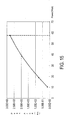
- FIG. 15 schematically illustrates the peak area-power diagram of a wavelength-converting device of the present invention.
- the peak area-power diagram of the wavelength-converting device 32 of the present invention applied to a high-energy illumination system is shown in FIG. 15 .
- the total peak value performance has a substantially linear growth.
- the wavelength-converting device 32 of the present invention can be applied to a high-power environment higher than 60 watts.
- the present invention provides an illumination system and a wavelength-converting device thereof.
- the phosphor plate is a solid mixture having 10-70 weight percent of phosphor agent and a binder for transforming the light in the first waveband into a light in a second waveband, the efficiency of heat conduction of the phosphor plate is effectively enhanced, thereby enhancing the conversion efficiency of the wavelength-converting device, which is strong enough to be applied to rotate with great rigidity.
- the wavelength-converting device is applied as a rotational wavelength-converting device without utilizing any heat sink, not only the space requirement is reduced, but also the phenomena of hot spot and heat diffusion are avoided, such that the cost and difficulty of manufacturing the wavelength-converting device are significantly reduced.
- polishing the light output surface of the phosphor plate and forming a polished surface the efficiency of receiving lights of the phosphor plate is enhanced, and further the conversion efficiency of the wavelength-converting device is also enhanced.
Landscapes
- Physics & Mathematics (AREA)
- Chemical & Material Sciences (AREA)
- General Physics & Mathematics (AREA)
- Engineering & Computer Science (AREA)
- Multimedia (AREA)
- Optics & Photonics (AREA)
- Inorganic Chemistry (AREA)
- Materials Engineering (AREA)
- Organic Chemistry (AREA)
- Projection Apparatus (AREA)
- Non-Portable Lighting Devices Or Systems Thereof (AREA)
Abstract
Description
- The present invention relates to an illumination system, and more particularly to an illumination system and a wavelength-converting device thereof.
- In recent years, high-end projectors utilize laser elements and wavelength-converting devices as illumination systems. The conventional wavelength-converting devices can be classified into two kinds of wavelength-converting device, one of which is a rotational phosphor wheel, and another one of which is a fixed phosphor plate module.
- Please refer to
FIG. 1 and FIG. 2. FIG. 1 schematically illustrates the structure of a rotational phosphor wheel of prior art.FIG. 2 schematically illustrates the structure of a fixed phosphor plate module of prior art. In arotational phosphor wheel 1, phosphor powder (or phosphor agent) 11 is mixed with adhesive glues and coated on a specific position of the high-reflective substrate 10, which is circle-shaped. The high-reflective substrate 10 is installed on amotor 12, so that the heat-dissipation may be implemented through rotating by therotational phosphor wheel 1 during performing wavelength conversions. On the other hand, since the heat-dissipation cannot be implemented through rotating by the fixed phosphor plate module 2, thephosphor plate 21 is generally mounted onto a surface of a high-reflective substrate 20, and aheat sink 22 is mounted on another surface of the high-reflective substrate 20. Under this circumstance, the heat generated by the laser source may be dissipated. - However, in the
rotational phosphor wheel 1, the conversion efficiency ofphosphor powder 11 is low because of low reliability and low thermal conductivity of adhesive glues. Meanwhile, the rigidity of the high-reflective substrate 10 may be not enough to be applied through rotation and shake. In addition, in the fixed phosphor plate module 2, the heat-dissipation of theheat sink 22 is mainly implemented through conduction and convection, so the high-reflective substrate 20 and theheat sink 22 have to be chosen from components having relatively larger surface area. That is, the space requirements often exceed expectations. Furthermore, the phenomena of hot spot and heat diffusion causes high manufacturing cost and difficulty of the fixed phosphor plate module 2. - There is a need of providing an illumination system and a wavelength-converting device thereof to obviate the drawbacks encountered from the prior art.
- It is an object of the present invention to provide an illumination system and a wavelength-converting device thereof in order to overcome the above-mentioned drawbacks encountered by the prior arts.
- The above problems are solved by an illumination system according to
claim 1 and by a wavelength-converting device for the illumination system according to claim 14. Further advantageous embodiments are the subject-matter of the dependent claims. - The present invention provides an illumination system and a wavelength-converting device thereof. Since the phosphor plate is a solid mixture, having 10-70 weight percent of phosphor agent and a binder, for transforming (converting) the light in the first waveband into light in a second waveband different from the first waveband, the efficiency of heat conduction of the phosphor plate is effectively enhanced, thereby enhancing the conversion efficiency of the wavelength-converting device, which is strong enough to be applied to rotate with great rigidity.
- The present invention also provides an illumination system and a wavelength-converting device thereof. The wavelength-converting device is applied as a rotational wavelength-converting device without utilizing any heat sink, not only the space requirement is reduced, but also the phenomena of hot spot and heat diffusion are avoided, such that the cost and difficulty of manufacturing the wavelength-converting device are significantly reduced.
- The present invention further provides an illumination system and a wavelength-converting device thereof. By polishing the light output surface of the phosphor plate and forming a polished surface, the efficiency of receiving lights of the phosphor plate is enhanced, and further the conversion efficiency of the wavelength-converting device is also enhanced.
- In accordance with an aspect of the present invention, there is provided an illumination system. The illumination system includes a solid-state light-emitting element and a wavelength-converting device. A light in a first waveband is emitted to an optical path by the solid-state light-emitting element. The wavelength-converting device is disposed on the optical path and includes a phosphor plate. The phosphor plate is a solid mixture having a phosphor agent and a binder. The weight percent of the phosphor agent is from 10 to 70, such that the light in the first waveband is transformed into light in the second waveband different from the first waveband.
- In accordance with another aspect of the present invention, there is provided a wavelength-converting device of an illumination system emitting a light in a first waveband to an optical path. The wavelength-converting device includes a phosphor plate disposed on the optical path for receiving the light in the first waveband, wherein the phosphor plate is a solid mixture having a phosphor agent and a binder, the weight percent of the phosphor agent is from 10 to 70, such that the light in the first waveband is transformed into light in a second waveband different from the first waveband.
- The above contents of the present invention will become more readily apparent to those ordinarily skilled in the art after reviewing the following detailed description and accompanying drawings, in which:
-
- FIG. 1
- schematically illustrates the structure of a rotational phosphor wheel of prior art;
- FIG. 2
- schematically illustrates the structure of a fixed phosphor plate module of prior art;
- FIG. 3A
- schematically illustrates the configuration of an illumination system according to an embodiment of the present invention;
- FIG. 3B
- schematically illustrates the configuration of an illumination system according to another embodiment of the present invention;
- FIG. 4
- schematically illustrates the cross-sectional view of a wavelength-converting device according to an embodiment of the present invention;
- FIG. 5
- schematically illustrates the cross-sectional view of a wavelength-converting device according to another embodiment of the present invention;
- FIG. 6
- schematically illustrates the cross-sectional view of a wavelength-converting device according to still another embodiment of the present invention;
- FIG. 7
- schematically illustrates the cross-sectional view of a wavelength-converting device according to still another embodiment of the present invention;
- FIG. 8
- schematically illustrates an air gap formed through adhering;
- FIG. 9
- schematically illustrates an air gap formed through clipping;
- FIG. 10
- schematically illustrates the scattering lights reflected by an optical layer of a transmissive wavelength-converting device;
- FIG. 11
- schematically illustrates the scattering lights reflected by an optical layer of a reflective wavelength-converting device;
- FIG. 12
- schematically illustrates the scattering lights reflected by an optical layer of a transmissive wavelength-converting device having a substrate;
- FIG. 13
- schematically illustrates the scattering lights reflected by an optical layer of a reflective wavelength-converting device having a substrate;
- FIG. 14
- schematically illustrates the performance voltage-pulse width diagram of a wavelength-converting device of the present invention and a conventional wavelength-converting device of prior art; and
- FIG. 15
- schematically illustrates the peak area-power diagram of a wavelength-converting device of the present invention.
- The present invention will now be described more specifically with reference to the following embodiments. It is to be noted that the following descriptions of preferred embodiments of this invention are presented herein for purpose of illustration and description only. It is not intended to be exhaustive or to be limited to the precise form disclosed.
- Please refer to
FIG. 3A and FIG. 3B. FIG. 3A schematically illustrates the configuration of an illumination system according to an embodiment of the present invention.FIG. 3B schematically illustrates the configuration of an illumination system according to another embodiment of the present invention. As shown inFIG. 3A and FIG. 3B , anillumination system 3 of the present invention includes a solid-state light-emittingelement 31 and a wavelength-convertingdevice 32. A light L1 in a first waveband is emitted to an optical path P by the solid-state light-emittingelement 31. The wavelength-convertingdevice 32 is disposed on the optical path P and includes aphosphor plate 321. Thephosphor plate 321 is a solid mixture having a phosphor agent and a binder. The weight percent of the phosphor agent is from 10 to 70 (compared with the total weight of the phosphor plate 321), the weight percent of the binder is for example from 30 to 90 (compared with the total weight of the phosphor plate 321), and the binder is for examples of glass or Al2O3, but not limited thereto, such that the light L1 in the first waveband is transformed into light L2 in a second waveband. In some embodiments, the wavelength-convertingdevice 32 is not limited to a transmissive wavelength-converting device (as shown inFIG. 3A ) or a reflective wavelength-converting device (as shown inFIG. 3B ). In other words, in the embodiments shown inFIG. 3A , the incident direction of the light L1 in the first waveband is identical to the output direction of the light L2 in the second waveband. In the embodiments shown inFIG. 3B , the incident direction of the light L1 in the first waveband is opposite to the output direction of the light L2 in the second waveband. As a result, the efficiency of heat conduction of thephosphor plate 321 is effectively enhanced, thereby enhancing the conversion efficiency of the wavelength-converting device, which is strong enough to be applied to rotate with great rigidity. - In some embodiments, the binder can be glass or Al2O3 as the embodiment mentioned above, or the binder may further includes ceramic additives, such like BaSO4, AlN and BN, for enhancing the efficiency of heat-dissipation. The formula of the glass is SiOx, 0<x□2, and the refraction coefficient n of the glass is less than or equal to 1.5. Compared with the applications of the combination of glass and phosphor powder in LED field, since the required refraction coefficient n of the glass in LED field is greater than or equal to 2, the differences between the applications in LED field and the present invention are obvious, and the concept of the present invention is distinct from the applications in LED field. Which is to say, the development direction of the wavelength-converting
device 32 of the present invention is opposite to the development direction of LED field, and the problems solved are also different. - Please refer to
FIG. 4 and FIG. 5. FIG. 4 schematically illustrates the cross-sectional view of a wavelength-converting device according to an embodiment of the present invention.FIG. 5 schematically illustrates the cross-sectional view of a wavelength-converting device according to another embodiment of the present invention. In some embodiments, the wavelength-convertingdevice 32 may be designed without substrate, and the wavelength-convertingdevice 32 may further include anoptical layer 322. Theoptical layer 322 is formed on a surface of thephosphor plate 321, and thephosphor plate 321 is not limited to a sheet phosphor plate (as shown inFIG. 4 ) or a ring-shaped phosphor plate (as shown inFIG. 5 ). In particular, theoptical layer 322 is deposited or coated on the surface of thephosphor plate 321, and theoptical layer 322 is disposed on a side in opposite to a light output surface of thephosphor plate 321. That is, the surface is disposed in opposite to the light output surface. - Please refer to
FIG. 6 and FIG. 7. FIG. 6 schematically illustrates the cross-sectional view of a wavelength-converting device according to still another embodiment of the present invention.FIG. 7 schematically illustrates the cross-sectional view of a wavelength-converting device according to still another embodiment of the present invention. In some embodiments, thephosphor plate 321 of the wavelength-convertingdevice 32 of the present invention is a sheet phosphor plate (as shown inFIG. 6 ) or a ring-shaped phosphor plate (as shown inFIG. 7 ). The wavelength-convertingdevice 32 may further include anoptical layer 322 and asubstrate 323, and theoptical layer 322 is formed on thesubstrate 323. Particularly, theoptical layer 322 is disposed on a side in opposite to a light output surface of thephosphor plate 321. On the other hand, the wavelength-converting device may further include abonding layer 325 disposed between theoptical layer 322 and thesubstrate 323, and the bonding layer is made of SiO2 or TiO2. - In the above-mentioned embodiments shown in
FIG. 4 to FIG. 7 , while being applied to a transmissive wavelength-converting device, theoptical layer 322 is preferably a dichroic layer for allowing the light L1 in the first waveband to transmit through and reflecting the light L2 in the second waveband. Contrary, while being applied to a reflective wavelength-converting device, theoptical layer 322 is preferably a all-reflective layer or a dichroic layer for comprehensively reflecting all of the light L1 in the first waveband and the light L2 in the second waveband, or reflecting only the light L2 in the second waveband. - Please refer to
FIG. 8 and FIG. 9. FIG. 8 schematically illustrates an air gap formed through adhering.FIG. 9 schematically illustrates an air gap formed through clipping. As shown inFIG. 8 and FIG. 9 , an air gap A is formed between thephosphor plate 321 and theoptical layer 322 for enhancing the optical properties, such like changing the refraction coefficient n, but not limited thereto. The air gap A is for example formed through adhering or clipping. As shown inFIG. 8 , thephosphor plate 321 and theoptical layer 322 is partially adhered with each other through the adhesive glue G, and the air gap is formed through adhering. As shown inFIG. 9 , thephosphor plate 321 and theoptical layer 322 are clipped together by the clipper C, and the air gap A is naturally formed between thephosphor plate 321 and theoptical layer 322. Nevertheless, the method of forming the air gap A is not limited herein. - Please refer to
FIG. 3A to FIG. 9 . The wavelength-convertingdevice 32 of the present invention can be installed on the axis of themotor 324 for being applied to rotate. As a result, the wavelength-convertingdevice 32 is applied as a rotational wavelength-converting device without utilizing any heat sink, not only the space requirement is reduced, but also the phenomena of hot spot and heat diffusion are avoided, such that the cost and difficulty of manufacturing the wavelength-convertingdevice 32 are significantly reduced. - Please refer to
FIG. 10 and FIG. 11. FIG. 10 schematically illustrates the scattering lights reflected by an optical layer of a transmissive wavelength-converting device.FIG. 11 schematically illustrates the scattering lights reflected by an optical layer of a reflective wavelength-converting device. As shown inFIG. 10 and FIG. 11 , after the light L1 in the first waveband is received by thephosphor plate 321 of the wavelength-convertingdevice 32, the light L1 in the first waveband is excited as a light L2 in the second waveband. The light L2 in the second waveband is configured as full-angle scattering. When a scattering light L20 is backscattered to theoptical layer 322, the scattering light L20 is reflected by theoptical layer 322 and outputted through the light output surface of thephosphor plate 321. That is, the higher the efficiency of reflection of theoptical layer 322 is, the better the efficiency of wavelength conversion of the wavelength-convertingdevice 32 is. - Please refer to
FIG. 12 and FIG. 13. FIG. 12 schematically illustrates the scattering lights reflected by an optical layer of a transmissive wavelength-converting device having a substrate.FIG. 13 schematically illustrates the scattering lights reflected by an optical layer of a reflective wavelength-converting device having a substrate. As shown inFIG. 12 and FIG. 13 , after the light L1 in the first waveband is received by thephosphor plate 321 of the wavelength-convertingdevice 32, the light L1 in the first waveband is excited as a light L2 in the second waveband by thephosphor plate 321. The light L2 in the second waveband is configured as full-angle scattering. When a large-angle scattering light L21 is backscattered to the air gap A, the large-angle scattering light L21 is total reflected by the air gap A and outputted through the light output surface. Moreover, when a small-angle scattering light L22 is backscattered to theoptical layer 322, the small-angle scattering light L22 is reflected by theoptical layer 322 and outputted through the light output surface. In other words, by forming the air gap A between thephosphor plate 321 and theoptical layer 322, the total reflection principle can be applied and the large-angle scattering light L21 can be outputted so as to be used for enhancing the efficiency of wavelength conversion of the wavelength-convertingdevice 32 of the present invention. - In some embodiments, the phosphor agent is not limited to monocrystalline phosphor powder or polycrystalline phosphor powder. In addition, functional additives, such like BN, AlN or BaSO4, may be added in the manufacturing process of the
phosphor plate 321, but not limited thereto. For providing high performance of optical reflection, theoptical layer 322 is preferably selected from at least one of Au, Ag, Al, or the group consisting of Au, Ag and Al. Certainly, theoptical layer 322 may be selected from dielectric materials. In some embodiments, thesubstrate 323 is a metal substrate, a ceramic substrate, a wafer substrate or a composition substrate. The material of the metal substrate is selected from Au, Ag, Al, or the alloys thereof. The material of the ceramic substrate is selected from AlN, BN, Al2O3, glass, and CaF2. The wafer substrate is a silicon wafer, a silicon carbide wafer, a silicon carbide, a sapphire and graphene wafer or any other compound semiconductor wafers groups. The composition substrate is a graphite substrate, a graphite and aluminum substrate or a graphite and silicon carbide substrate, but not limited thereto. - In some embodiments, the thickness of the
phosphor plate 321 of the wavelength-convertingdevice 32 of the present invention is preferably greater than or equal to 50 micrometers (um), and less than or equal to 1000 micrometers (um). In an embodiment, thephosphor plate 321 is sintered by 20 weight percent of phosphor agent and 80 weight percent of glass. The thickness and the diameter of thephosphor plate 321 are respectively 540 mm and 10 cm, but not limited herein. According to the experimental results of this embodiment, although the weight percent of the phosphor agent is only 20, a gain of at least 15% is obtained by the present invention compared with the prior art, which has phosphor powder about 70 weight percent. Since the proportion of the phosphor agent of the present invention is from 10 to 70 weight percent and the thickness of thephosphor plate 321 is from 50 to 1000 mm, the maximum of the gain is not limited herein. - On the other hand, the light output surface of the
phosphor plate 321 is polished as a polished surface for enhancing the optical properties of the wavelength-convertingdevice 32. As a result, the efficiency of receiving lights of thephosphor plate 321 is enhanced, and further the efficiency of wavelength conversion of the wavelength-convertingdevice 32 is also enhanced. - Please refer to
FIG. 14. FIG. 14 schematically illustrates the performance voltage-pulse width diagram of a wavelength-converting device of the present invention and a conventional wavelength-converting device of prior art. As shown inFIG. 14 , when the solid-state light-emittingelement 31 is a laser source, the driving current of the laser source is 2.3A, and the output power is 3.5W, since the conventional adhesive phosphor wheel has the worst efficiency of heat-dissipation, the performance gets a fastest decay. The total performance of the conventional adhesive phosphor wheel is also the worst. In addition, when a phosphor wheel is manufactured by utilizing YAG phosphor powder, the performance of the phosphor wheel is ordinary. However, the decay of the performance is reduced compared with the conventional adhesive phosphor wheel, hence the performance of the phosphor wheel is obviously better than the performance of the conventional adhesive phosphor wheel. On the other hand, the performance of the wavelength-convertingdevice 32 of the present invention is obviously better than the phosphor wheel, and the decay rate and decay extent are the smallest of these three examples. In brief, compared with the conventional adhesive phosphor wheel and the (pure) phosphor wheel, the wavelength-convertingdevice 32 of the present invention has the best performances. - Please refer to
FIG. 15. FIG. 15 schematically illustrates the peak area-power diagram of a wavelength-converting device of the present invention. The peak area-power diagram of the wavelength-convertingdevice 32 of the present invention applied to a high-energy illumination system is shown inFIG. 15 . When the output power of the solid-state light-emittingelement 31 is continuously increased, the total peak value performance has a substantially linear growth. According to the experimental results, the wavelength-convertingdevice 32 of the present invention can be applied to a high-power environment higher than 60 watts. - From the above description, the present invention provides an illumination system and a wavelength-converting device thereof. Since the phosphor plate is a solid mixture having 10-70 weight percent of phosphor agent and a binder for transforming the light in the first waveband into a light in a second waveband, the efficiency of heat conduction of the phosphor plate is effectively enhanced, thereby enhancing the conversion efficiency of the wavelength-converting device, which is strong enough to be applied to rotate with great rigidity. Meanwhile, the wavelength-converting device is applied as a rotational wavelength-converting device without utilizing any heat sink, not only the space requirement is reduced, but also the phenomena of hot spot and heat diffusion are avoided, such that the cost and difficulty of manufacturing the wavelength-converting device are significantly reduced. Moreover, by polishing the light output surface of the phosphor plate and forming a polished surface, the efficiency of receiving lights of the phosphor plate is enhanced, and further the conversion efficiency of the wavelength-converting device is also enhanced.
Claims (20)
- An illumination system (3), comprising:a solid-state light-emitting element (31), wherein a light (L1) in a first waveband is emitted to an optical path (P) by the solid-state light-emitting element (31); anda wavelength-converting device (32) disposed on the optical path (P) and comprising a phosphor plate (321), wherein the phosphor plate (321) is a solid mixture having a phosphor agent and a binder, the weight percent of the phosphor agent is from 10 to 70, such that the light (L1) in the first waveband is transformed into a light (L2) in a second waveband.
- The illumination system according to claim 1, wherein the binder is glass or Al2O3, wherein the formula of the glass is SiOx, 0<x≦2, and the refraction coefficient n of the glass is less than or equal to 1.5.
- The illumination system according to claim 2, wherein the binder further comprises ceramic additives.
- The illumination system according to claim 1, wherein the phosphor plate (321) is a ring-shaped phosphor plate or a sheet phosphor plate.
- The illumination system according to claim 1, wherein the wavelength-converting device (32) further comprises an optical layer (322) formed on a surface of the phosphor plate (321).
- The illumination system according to claim 5, wherein the optical layer (322) is deposited or coated on the surface of the phosphor plate (321), and the optical layer (322) is disposed on a side in opposite to a light output surface of the phosphor plate (321).
- The illumination system according to claim 1, wherein the wavelength-converting device (32) further comprises a substrate (323) and an optical layer (322), and the optical layer (322) is formed on the substrate (323).
- The illumination system according to claim 7, wherein the optical layer (322) is disposed on a side in opposite to a light output surface of the phosphor plate (321).
- The illumination system according to claim 8, wherein the light output surface is a polished surface.
- The illumination system according to claim 7, wherein an air gap (A) is formed between the phosphor plate (321) and the optical layer (322) formed on the substrate (323), and the air gap (A) is formed through adhering or clipping.
- The illumination system according to claim 7, wherein the wavelength-converting device (32) further comprises a bonding layer (325) disposed between the optical layer (322) and the substrate (323).
- The illumination system according to claim 11, wherein the bonding layer (325) is made of SiO2 or TiO2.
- The illumination system according to claim 1, wherein the thickness of the phosphor plate (321) is greater than or equal to 50 micrometers, and is less than or equal to 1000 micrometers.
- A wavelength-converting device (32) for an illumination system (3) emitting a light (L1) in a first waveband to an optical path (P), comprising:a phosphor plate (321) disposed on the optical path (P) for receiving the light (L1) in the first waveband, wherein the phosphor plate (321) is a solid mixture having a phosphor agent and a binder, the weight percent of the phosphor agent is from 10 to 70, such that the light (L1) in the first waveband is transformed into a light (L2) in a second waveband.
- The wavelength-converting device according to claim 14 further comprising an optical layer (322) formed on a surface of the phosphor plate (321).
- The wavelength-converting device according to claim 15, wherein the optical layer (322) is deposited or coated on the surface of the phosphor plate (321), and the optical layer (322) is disposed on a side in opposite to a light output surface of the phosphor plate (321).
- The wavelength-converting device according to claim 16, wherein the light output surface is a polished surface.
- The wavelength-converting device according to claim 14 further comprising a substrate (323) and an optical layer (322), wherein the optical layer (322) is formed on the substrate (323).
- The wavelength-converting device according to claim 18, wherein the optical layer (322) is disposed on a side in opposite to a light output surface of the phosphor plate (321), and the light output surface is a polished surface.
- The wavelength-converting device according to claim 18 further comprising a bonding layer (325) disposed between the optical layer (322) and the substrate (323), wherein the bonding layer (325) is made of SiO2 or TiO2.
Applications Claiming Priority (2)
| Application Number | Priority Date | Filing Date | Title |
|---|---|---|---|
| US201461984418P | 2014-04-25 | 2014-04-25 | |
| TW103143268A TWI617059B (en) | 2014-04-25 | 2014-12-11 | Illumination system and wavelength-converting deivce thereof |
Publications (3)
| Publication Number | Publication Date |
|---|---|
| EP2955573A1 true EP2955573A1 (en) | 2015-12-16 |
| EP2955573B1 EP2955573B1 (en) | 2019-02-06 |
| EP2955573B8 EP2955573B8 (en) | 2019-03-20 |
Family
ID=54334398
Family Applications (1)
| Application Number | Title | Priority Date | Filing Date |
|---|---|---|---|
| EP15163559.6A Active EP2955573B8 (en) | 2014-04-25 | 2015-04-14 | Illumination system and wavelength-converting device thereof |
Country Status (2)
| Country | Link |
|---|---|
| US (1) | US9891511B2 (en) |
| EP (1) | EP2955573B8 (en) |
Families Citing this family (8)
| Publication number | Priority date | Publication date | Assignee | Title |
|---|---|---|---|---|
| JP6536212B2 (en) * | 2015-06-23 | 2019-07-03 | セイコーエプソン株式会社 | Wavelength conversion element, light source device and projector |
| JP6740616B2 (en) * | 2015-09-15 | 2020-08-19 | 日本電気硝子株式会社 | Wavelength conversion member and light emitting device |
| WO2017220411A1 (en) | 2016-06-22 | 2017-12-28 | Lumileds Holding B.V. | Light conversion package |
| CN111033366B (en) * | 2017-08-17 | 2023-02-28 | 索尼公司 | Light source device and projection display device |
| JP7200673B2 (en) * | 2018-12-28 | 2023-01-10 | セイコーエプソン株式会社 | Light source device and projector |
| CN112578552A (en) | 2019-09-30 | 2021-03-30 | 台达电子工业股份有限公司 | Wavelength conversion device |
| CN112578551A (en) | 2019-09-30 | 2021-03-30 | 台达电子工业股份有限公司 | Wavelength conversion device |
| CN113970872A (en) | 2020-07-24 | 2022-01-25 | 中强光电股份有限公司 | Wavelength conversion element and projector |
Citations (4)
| Publication number | Priority date | Publication date | Assignee | Title |
|---|---|---|---|---|
| JP2011129406A (en) * | 2009-12-18 | 2011-06-30 | Stanley Electric Co Ltd | Light source device and lighting system |
| US20110279012A1 (en) * | 2010-05-12 | 2011-11-17 | Takashi Washizu | Wavelength conversion element and light emitting device |
| WO2012138020A1 (en) * | 2011-04-04 | 2012-10-11 | Lg Electronics Inc. | Light source apparatus and method for manufacturing the same |
| WO2013055552A2 (en) * | 2011-10-13 | 2013-04-18 | Intematix Corporation | Wavelength conversion component having photo-luminescence material embedded into a hermetic material for remote wavelength conversion |
Family Cites Families (14)
| Publication number | Priority date | Publication date | Assignee | Title |
|---|---|---|---|---|
| TWI280425B (en) | 2002-12-20 | 2007-05-01 | Hon Hai Prec Ind Co Ltd | Method of fabricating light guide plate having diffusion function |
| US7341878B2 (en) | 2005-03-14 | 2008-03-11 | Philips Lumileds Lighting Company, Llc | Wavelength-converted semiconductor light emitting device |
| JP5257687B2 (en) | 2009-02-23 | 2013-08-07 | カシオ計算機株式会社 | Light source device and projector |
| US8556437B2 (en) * | 2009-12-17 | 2013-10-15 | Stanley Electric Co., Ltd. | Semiconductor light source apparatus and lighting unit |
| WO2012014360A1 (en) | 2010-07-26 | 2012-02-02 | 株式会社小糸製作所 | Light-emitting module |
| MY164263A (en) | 2010-12-29 | 2017-11-30 | 3M Innovative Properties Co | Phosphor refletor assembly for remote phosphor led device |
| JP2012243618A (en) | 2011-05-20 | 2012-12-10 | Stanley Electric Co Ltd | Light source device and lighting device |
| JP5818134B2 (en) | 2011-05-24 | 2015-11-18 | スタンレー電気株式会社 | Vehicle headlamp |
| CN102854726B (en) * | 2011-06-27 | 2015-07-29 | 深圳市绎立锐光科技开发有限公司 | Phosphor layer, device, corresponding light source and projection system, and corresponding manufacturing method |
| US9134595B2 (en) * | 2011-09-29 | 2015-09-15 | Casio Computer Co., Ltd. | Phosphor device, illumination apparatus and projector apparatus |
| CN103045256B (en) | 2011-10-17 | 2014-08-27 | 有研稀土新材料股份有限公司 | LED (Light Emitting Diode) red fluorescence material and luminescent device containing same |
| CN104865670B (en) | 2011-11-12 | 2018-03-06 | 深圳市光峰光电技术有限公司 | Colour wheel, its assemble method and the light source using the colour wheel |
| JP5962904B2 (en) * | 2012-04-26 | 2016-08-03 | パナソニックIpマネジメント株式会社 | Light source device and projection display device including the light source device |
| JP2013122930A (en) | 2013-02-07 | 2013-06-20 | Casio Computer Co Ltd | Light-emitting device and light source device as well as projector using the latter |
-
2015
- 2015-04-14 EP EP15163559.6A patent/EP2955573B8/en active Active
- 2015-04-14 US US14/686,321 patent/US9891511B2/en active Active
Patent Citations (4)
| Publication number | Priority date | Publication date | Assignee | Title |
|---|---|---|---|---|
| JP2011129406A (en) * | 2009-12-18 | 2011-06-30 | Stanley Electric Co Ltd | Light source device and lighting system |
| US20110279012A1 (en) * | 2010-05-12 | 2011-11-17 | Takashi Washizu | Wavelength conversion element and light emitting device |
| WO2012138020A1 (en) * | 2011-04-04 | 2012-10-11 | Lg Electronics Inc. | Light source apparatus and method for manufacturing the same |
| WO2013055552A2 (en) * | 2011-10-13 | 2013-04-18 | Intematix Corporation | Wavelength conversion component having photo-luminescence material embedded into a hermetic material for remote wavelength conversion |
Also Published As
| Publication number | Publication date |
|---|---|
| US20150308637A1 (en) | 2015-10-29 |
| US9891511B2 (en) | 2018-02-13 |
| EP2955573B8 (en) | 2019-03-20 |
| EP2955573B1 (en) | 2019-02-06 |
Similar Documents
| Publication | Publication Date | Title |
|---|---|---|
| EP2955573B1 (en) | Illumination system and wavelength-converting device thereof | |
| TWI617059B (en) | Illumination system and wavelength-converting deivce thereof | |
| CN105423238B (en) | Wavelength conversion member, light emitting device, projector, and method of manufacturing wavelength conversion member | |
| US10794569B2 (en) | Wavelength conversion member, light source and lighting device | |
| US10865950B2 (en) | Light source unit and projection-type display | |
| US10578957B2 (en) | Fluorescent substrate, light source device, and projection display unit | |
| JP2013207049A (en) | Light emitting device using wavelength conversion body | |
| CN105637404A (en) | Fluorescent wheel for projector and light emitting device for projector | |
| JP2010537411A (en) | Optoelectronic semiconductor module and manufacturing method thereof | |
| KR102733802B1 (en) | Reflection Color Correction for Phosphor Lighting Systems | |
| CN110737085A (en) | Wavelength conversion device | |
| US20200271282A1 (en) | Light-emitting element and illumination device | |
| CN111699420A (en) | Optical wavelength conversion device | |
| US11333806B2 (en) | Reliable light conversion device for laser-based light sources | |
| JP2016100090A (en) | Light-emitting module and light-emitting device using the same | |
| US20150372198A1 (en) | Light emitting module | |
| JP2016058619A (en) | Light emitting device | |
| JP2012243618A (en) | Light source device and lighting device | |
| CN112578552A (en) | Wavelength conversion device | |
| JP2015211034A (en) | Illumination system and wavelength conversion device | |
| EP3753055A1 (en) | Remote wavelength-converting member and related systems | |
| CN113383253A (en) | Wavelength conversion member and projector | |
| WO2017064951A1 (en) | Light source device | |
| US11353168B2 (en) | Wavelength conversion device | |
| CN110050223A (en) | Light-switching device |
Legal Events
| Date | Code | Title | Description |
|---|---|---|---|
| PUAI | Public reference made under article 153(3) epc to a published international application that has entered the european phase |
Free format text: ORIGINAL CODE: 0009012 |
|
| 17P | Request for examination filed |
Effective date: 20150414 |
|
| AK | Designated contracting states |
Kind code of ref document: A1 Designated state(s): AL AT BE BG CH CY CZ DE DK EE ES FI FR GB GR HR HU IE IS IT LI LT LU LV MC MK MT NL NO PL PT RO RS SE SI SK SM TR |
|
| AX | Request for extension of the european patent |
Extension state: BA ME |
|
| RIC1 | Information provided on ipc code assigned before grant |
Ipc: C09K 11/02 20060101ALN20180919BHEP Ipc: H01L 33/64 20100101ALN20180919BHEP Ipc: G03B 21/16 20060101AFI20180919BHEP Ipc: G03B 21/20 20060101ALI20180919BHEP |
|
| GRAP | Despatch of communication of intention to grant a patent |
Free format text: ORIGINAL CODE: EPIDOSNIGR1 |
|
| STAA | Information on the status of an ep patent application or granted ep patent |
Free format text: STATUS: GRANT OF PATENT IS INTENDED |
|
| RIC1 | Information provided on ipc code assigned before grant |
Ipc: G03B 21/20 20060101ALI20181011BHEP Ipc: H01L 33/64 20100101ALN20181011BHEP Ipc: C09K 11/02 20060101ALN20181011BHEP Ipc: G03B 21/16 20060101AFI20181011BHEP |
|
| INTG | Intention to grant announced |
Effective date: 20181029 |
|
| GRAS | Grant fee paid |
Free format text: ORIGINAL CODE: EPIDOSNIGR3 |
|
| GRAA | (expected) grant |
Free format text: ORIGINAL CODE: 0009210 |
|
| STAA | Information on the status of an ep patent application or granted ep patent |
Free format text: STATUS: THE PATENT HAS BEEN GRANTED |
|
| GRAT | Correction requested after decision to grant or after decision to maintain patent in amended form |
Free format text: ORIGINAL CODE: EPIDOSNCDEC |
|
| AK | Designated contracting states |
Kind code of ref document: B1 Designated state(s): AL AT BE BG CH CY CZ DE DK EE ES FI FR GB GR HR HU IE IS IT LI LT LU LV MC MK MT NL NO PL PT RO RS SE SI SK SM TR |
|
| REG | Reference to a national code |
Ref country code: GB Ref legal event code: FG4D |
|
| REG | Reference to a national code |
Ref country code: CH Ref legal event code: EP Ref country code: AT Ref legal event code: REF Ref document number: 1095275 Country of ref document: AT Kind code of ref document: T Effective date: 20190215 |
|
| RAP2 | Party data changed (patent owner data changed or rights of a patent transferred) |
Owner name: DELTA ELECTRONICS, INC. |
|
| REG | Reference to a national code |
Ref country code: DE Ref legal event code: R082 Ref document number: 602015024262 Country of ref document: DE Representative=s name: 2K PATENTANWAELTE BLASBERG KEWITZ & REICHEL PA, DE |
|
| REG | Reference to a national code |
Ref country code: CH Ref legal event code: PK Free format text: BERICHTIGUNG B8 |
|
| REG | Reference to a national code |
Ref country code: IE Ref legal event code: FG4D |
|
| REG | Reference to a national code |
Ref country code: DE Ref legal event code: R096 Ref document number: 602015024262 Country of ref document: DE |
|
| REG | Reference to a national code |
Ref country code: NL Ref legal event code: MP Effective date: 20190206 |
|
| REG | Reference to a national code |
Ref country code: LT Ref legal event code: MG4D |
|
| PG25 | Lapsed in a contracting state [announced via postgrant information from national office to epo] |
Ref country code: SE Free format text: LAPSE BECAUSE OF FAILURE TO SUBMIT A TRANSLATION OF THE DESCRIPTION OR TO PAY THE FEE WITHIN THE PRESCRIBED TIME-LIMIT Effective date: 20190206 Ref country code: NO Free format text: LAPSE BECAUSE OF FAILURE TO SUBMIT A TRANSLATION OF THE DESCRIPTION OR TO PAY THE FEE WITHIN THE PRESCRIBED TIME-LIMIT Effective date: 20190506 Ref country code: FI Free format text: LAPSE BECAUSE OF FAILURE TO SUBMIT A TRANSLATION OF THE DESCRIPTION OR TO PAY THE FEE WITHIN THE PRESCRIBED TIME-LIMIT Effective date: 20190206 Ref country code: PT Free format text: LAPSE BECAUSE OF FAILURE TO SUBMIT A TRANSLATION OF THE DESCRIPTION OR TO PAY THE FEE WITHIN THE PRESCRIBED TIME-LIMIT Effective date: 20190606 Ref country code: LT Free format text: LAPSE BECAUSE OF FAILURE TO SUBMIT A TRANSLATION OF THE DESCRIPTION OR TO PAY THE FEE WITHIN THE PRESCRIBED TIME-LIMIT Effective date: 20190206 Ref country code: NL Free format text: LAPSE BECAUSE OF FAILURE TO SUBMIT A TRANSLATION OF THE DESCRIPTION OR TO PAY THE FEE WITHIN THE PRESCRIBED TIME-LIMIT Effective date: 20190206 |
|
| REG | Reference to a national code |
Ref country code: AT Ref legal event code: MK05 Ref document number: 1095275 Country of ref document: AT Kind code of ref document: T Effective date: 20190206 |
|
| PG25 | Lapsed in a contracting state [announced via postgrant information from national office to epo] |
Ref country code: BG Free format text: LAPSE BECAUSE OF FAILURE TO SUBMIT A TRANSLATION OF THE DESCRIPTION OR TO PAY THE FEE WITHIN THE PRESCRIBED TIME-LIMIT Effective date: 20190506 Ref country code: GR Free format text: LAPSE BECAUSE OF FAILURE TO SUBMIT A TRANSLATION OF THE DESCRIPTION OR TO PAY THE FEE WITHIN THE PRESCRIBED TIME-LIMIT Effective date: 20190507 Ref country code: HR Free format text: LAPSE BECAUSE OF FAILURE TO SUBMIT A TRANSLATION OF THE DESCRIPTION OR TO PAY THE FEE WITHIN THE PRESCRIBED TIME-LIMIT Effective date: 20190206 Ref country code: IS Free format text: LAPSE BECAUSE OF FAILURE TO SUBMIT A TRANSLATION OF THE DESCRIPTION OR TO PAY THE FEE WITHIN THE PRESCRIBED TIME-LIMIT Effective date: 20190606 Ref country code: RS Free format text: LAPSE BECAUSE OF FAILURE TO SUBMIT A TRANSLATION OF THE DESCRIPTION OR TO PAY THE FEE WITHIN THE PRESCRIBED TIME-LIMIT Effective date: 20190206 Ref country code: LV Free format text: LAPSE BECAUSE OF FAILURE TO SUBMIT A TRANSLATION OF THE DESCRIPTION OR TO PAY THE FEE WITHIN THE PRESCRIBED TIME-LIMIT Effective date: 20190206 |
|
| PG25 | Lapsed in a contracting state [announced via postgrant information from national office to epo] |
Ref country code: SK Free format text: LAPSE BECAUSE OF FAILURE TO SUBMIT A TRANSLATION OF THE DESCRIPTION OR TO PAY THE FEE WITHIN THE PRESCRIBED TIME-LIMIT Effective date: 20190206 Ref country code: RO Free format text: LAPSE BECAUSE OF FAILURE TO SUBMIT A TRANSLATION OF THE DESCRIPTION OR TO PAY THE FEE WITHIN THE PRESCRIBED TIME-LIMIT Effective date: 20190206 Ref country code: CZ Free format text: LAPSE BECAUSE OF FAILURE TO SUBMIT A TRANSLATION OF THE DESCRIPTION OR TO PAY THE FEE WITHIN THE PRESCRIBED TIME-LIMIT Effective date: 20190206 Ref country code: DK Free format text: LAPSE BECAUSE OF FAILURE TO SUBMIT A TRANSLATION OF THE DESCRIPTION OR TO PAY THE FEE WITHIN THE PRESCRIBED TIME-LIMIT Effective date: 20190206 Ref country code: IT Free format text: LAPSE BECAUSE OF FAILURE TO SUBMIT A TRANSLATION OF THE DESCRIPTION OR TO PAY THE FEE WITHIN THE PRESCRIBED TIME-LIMIT Effective date: 20190206 Ref country code: EE Free format text: LAPSE BECAUSE OF FAILURE TO SUBMIT A TRANSLATION OF THE DESCRIPTION OR TO PAY THE FEE WITHIN THE PRESCRIBED TIME-LIMIT Effective date: 20190206 Ref country code: ES Free format text: LAPSE BECAUSE OF FAILURE TO SUBMIT A TRANSLATION OF THE DESCRIPTION OR TO PAY THE FEE WITHIN THE PRESCRIBED TIME-LIMIT Effective date: 20190206 Ref country code: AL Free format text: LAPSE BECAUSE OF FAILURE TO SUBMIT A TRANSLATION OF THE DESCRIPTION OR TO PAY THE FEE WITHIN THE PRESCRIBED TIME-LIMIT Effective date: 20190206 |
|
| REG | Reference to a national code |
Ref country code: DE Ref legal event code: R097 Ref document number: 602015024262 Country of ref document: DE |
|
| PG25 | Lapsed in a contracting state [announced via postgrant information from national office to epo] |
Ref country code: PL Free format text: LAPSE BECAUSE OF FAILURE TO SUBMIT A TRANSLATION OF THE DESCRIPTION OR TO PAY THE FEE WITHIN THE PRESCRIBED TIME-LIMIT Effective date: 20190206 Ref country code: SM Free format text: LAPSE BECAUSE OF FAILURE TO SUBMIT A TRANSLATION OF THE DESCRIPTION OR TO PAY THE FEE WITHIN THE PRESCRIBED TIME-LIMIT Effective date: 20190206 |
|
| REG | Reference to a national code |
Ref country code: CH Ref legal event code: PL |
|
| PLBE | No opposition filed within time limit |
Free format text: ORIGINAL CODE: 0009261 |
|
| STAA | Information on the status of an ep patent application or granted ep patent |
Free format text: STATUS: NO OPPOSITION FILED WITHIN TIME LIMIT |
|
| REG | Reference to a national code |
Ref country code: BE Ref legal event code: MM Effective date: 20190430 |
|
| PG25 | Lapsed in a contracting state [announced via postgrant information from national office to epo] |
Ref country code: AT Free format text: LAPSE BECAUSE OF FAILURE TO SUBMIT A TRANSLATION OF THE DESCRIPTION OR TO PAY THE FEE WITHIN THE PRESCRIBED TIME-LIMIT Effective date: 20190206 Ref country code: LU Free format text: LAPSE BECAUSE OF NON-PAYMENT OF DUE FEES Effective date: 20190414 Ref country code: MC Free format text: LAPSE BECAUSE OF FAILURE TO SUBMIT A TRANSLATION OF THE DESCRIPTION OR TO PAY THE FEE WITHIN THE PRESCRIBED TIME-LIMIT Effective date: 20190206 |
|
| 26N | No opposition filed |
Effective date: 20191107 |
|
| PG25 | Lapsed in a contracting state [announced via postgrant information from national office to epo] |
Ref country code: LI Free format text: LAPSE BECAUSE OF NON-PAYMENT OF DUE FEES Effective date: 20190430 Ref country code: CH Free format text: LAPSE BECAUSE OF NON-PAYMENT OF DUE FEES Effective date: 20190430 |
|
| PG25 | Lapsed in a contracting state [announced via postgrant information from national office to epo] |
Ref country code: SI Free format text: LAPSE BECAUSE OF FAILURE TO SUBMIT A TRANSLATION OF THE DESCRIPTION OR TO PAY THE FEE WITHIN THE PRESCRIBED TIME-LIMIT Effective date: 20190206 Ref country code: BE Free format text: LAPSE BECAUSE OF NON-PAYMENT OF DUE FEES Effective date: 20190430 |
|
| PG25 | Lapsed in a contracting state [announced via postgrant information from national office to epo] |
Ref country code: TR Free format text: LAPSE BECAUSE OF FAILURE TO SUBMIT A TRANSLATION OF THE DESCRIPTION OR TO PAY THE FEE WITHIN THE PRESCRIBED TIME-LIMIT Effective date: 20190206 |
|
| PG25 | Lapsed in a contracting state [announced via postgrant information from national office to epo] |
Ref country code: IE Free format text: LAPSE BECAUSE OF NON-PAYMENT OF DUE FEES Effective date: 20190414 |
|
| PG25 | Lapsed in a contracting state [announced via postgrant information from national office to epo] |
Ref country code: CY Free format text: LAPSE BECAUSE OF FAILURE TO SUBMIT A TRANSLATION OF THE DESCRIPTION OR TO PAY THE FEE WITHIN THE PRESCRIBED TIME-LIMIT Effective date: 20190206 |
|
| PG25 | Lapsed in a contracting state [announced via postgrant information from national office to epo] |
Ref country code: MT Free format text: LAPSE BECAUSE OF FAILURE TO SUBMIT A TRANSLATION OF THE DESCRIPTION OR TO PAY THE FEE WITHIN THE PRESCRIBED TIME-LIMIT Effective date: 20190206 Ref country code: HU Free format text: LAPSE BECAUSE OF FAILURE TO SUBMIT A TRANSLATION OF THE DESCRIPTION OR TO PAY THE FEE WITHIN THE PRESCRIBED TIME-LIMIT; INVALID AB INITIO Effective date: 20150414 |
|
| PG25 | Lapsed in a contracting state [announced via postgrant information from national office to epo] |
Ref country code: MK Free format text: LAPSE BECAUSE OF FAILURE TO SUBMIT A TRANSLATION OF THE DESCRIPTION OR TO PAY THE FEE WITHIN THE PRESCRIBED TIME-LIMIT Effective date: 20190206 |
|
| PGFP | Annual fee paid to national office [announced via postgrant information from national office to epo] |
Ref country code: DE Payment date: 20250429 Year of fee payment: 11 |
|
| PGFP | Annual fee paid to national office [announced via postgrant information from national office to epo] |
Ref country code: FR Payment date: 20250425 Year of fee payment: 11 |
|
| PGFP | Annual fee paid to national office [announced via postgrant information from national office to epo] |
Ref country code: GB Payment date: 20260327 Year of fee payment: 12 |