EP2953235A1 - Wireless power transfer system, power receiver, and wireless power transfer method - Google Patents
Wireless power transfer system, power receiver, and wireless power transfer method Download PDFInfo
- Publication number
- EP2953235A1 EP2953235A1 EP13873369.6A EP13873369A EP2953235A1 EP 2953235 A1 EP2953235 A1 EP 2953235A1 EP 13873369 A EP13873369 A EP 13873369A EP 2953235 A1 EP2953235 A1 EP 2953235A1
- Authority
- EP
- European Patent Office
- Prior art keywords
- power
- power receiver
- power source
- resonance
- coil
- Prior art date
- Legal status (The legal status is an assumption and is not a legal conclusion. Google has not performed a legal analysis and makes no representation as to the accuracy of the status listed.)
- Granted
Links
Images







Classifications
-
- H—ELECTRICITY
- H04—ELECTRIC COMMUNICATION TECHNIQUE
- H04B—TRANSMISSION
- H04B5/00—Near-field transmission systems, e.g. inductive or capacitive transmission systems
- H04B5/70—Near-field transmission systems, e.g. inductive or capacitive transmission systems specially adapted for specific purposes
- H04B5/79—Near-field transmission systems, e.g. inductive or capacitive transmission systems specially adapted for specific purposes for data transfer in combination with power transfer
-
- H—ELECTRICITY
- H02—GENERATION; CONVERSION OR DISTRIBUTION OF ELECTRIC POWER
- H02J—ELECTRIC POWER NETWORKS; CIRCUIT ARRANGEMENTS OR SYSTEMS FOR SUPPLYING OR DISTRIBUTING ELECTRIC POWER; SYSTEMS FOR STORING ELECTRIC ENERGY
- H02J50/00—Circuit arrangements or systems for wireless supply or distribution of electric power
- H02J50/05—Circuit arrangements or systems for wireless supply or distribution of electric power using capacitive coupling
-
- H—ELECTRICITY
- H02—GENERATION; CONVERSION OR DISTRIBUTION OF ELECTRIC POWER
- H02J—ELECTRIC POWER NETWORKS; CIRCUIT ARRANGEMENTS OR SYSTEMS FOR SUPPLYING OR DISTRIBUTING ELECTRIC POWER; SYSTEMS FOR STORING ELECTRIC ENERGY
- H02J50/00—Circuit arrangements or systems for wireless supply or distribution of electric power
- H02J50/10—Circuit arrangements or systems for wireless supply or distribution of electric power using inductive coupling
- H02J50/12—Circuit arrangements or systems for wireless supply or distribution of electric power using inductive coupling of the resonant type
-
- H—ELECTRICITY
- H02—GENERATION; CONVERSION OR DISTRIBUTION OF ELECTRIC POWER
- H02J—ELECTRIC POWER NETWORKS; CIRCUIT ARRANGEMENTS OR SYSTEMS FOR SUPPLYING OR DISTRIBUTING ELECTRIC POWER; SYSTEMS FOR STORING ELECTRIC ENERGY
- H02J50/00—Circuit arrangements or systems for wireless supply or distribution of electric power
- H02J50/40—Circuit arrangements or systems for wireless supply or distribution of electric power using two or more transmitting or receiving devices
-
- H—ELECTRICITY
- H02—GENERATION; CONVERSION OR DISTRIBUTION OF ELECTRIC POWER
- H02J—ELECTRIC POWER NETWORKS; CIRCUIT ARRANGEMENTS OR SYSTEMS FOR SUPPLYING OR DISTRIBUTING ELECTRIC POWER; SYSTEMS FOR STORING ELECTRIC ENERGY
- H02J50/00—Circuit arrangements or systems for wireless supply or distribution of electric power
- H02J50/80—Circuit arrangements or systems for wireless supply or distribution of electric power involving the exchange of data, concerning supply or distribution of electric power, between transmitting devices and receiving devices
-
- H—ELECTRICITY
- H02—GENERATION; CONVERSION OR DISTRIBUTION OF ELECTRIC POWER
- H02J—ELECTRIC POWER NETWORKS; CIRCUIT ARRANGEMENTS OR SYSTEMS FOR SUPPLYING OR DISTRIBUTING ELECTRIC POWER; SYSTEMS FOR STORING ELECTRIC ENERGY
- H02J50/00—Circuit arrangements or systems for wireless supply or distribution of electric power
- H02J50/90—Circuit arrangements or systems for wireless supply or distribution of electric power involving detection or optimisation of position, e.g. alignment
-
- H—ELECTRICITY
- H02—GENERATION; CONVERSION OR DISTRIBUTION OF ELECTRIC POWER
- H02J—ELECTRIC POWER NETWORKS; CIRCUIT ARRANGEMENTS OR SYSTEMS FOR SUPPLYING OR DISTRIBUTING ELECTRIC POWER; SYSTEMS FOR STORING ELECTRIC ENERGY
- H02J7/00—Circuit arrangements for charging or discharging batteries or for supplying loads from batteries
- H02J7/40—Circuit arrangements for charging or discharging batteries or for supplying loads from batteries characterised by the exchange of charge or discharge related data
- H02J7/42—Circuit arrangements for charging or discharging batteries or for supplying loads from batteries characterised by the exchange of charge or discharge related data with electronic devices having internal batteries, e.g. mobile phones
-
- H—ELECTRICITY
- H04—ELECTRIC COMMUNICATION TECHNIQUE
- H04B—TRANSMISSION
- H04B5/00—Near-field transmission systems, e.g. inductive or capacitive transmission systems
- H04B5/20—Near-field transmission systems, e.g. inductive or capacitive transmission systems characterised by the transmission technique; characterised by the transmission medium
- H04B5/22—Capacitive coupling
-
- H—ELECTRICITY
- H04—ELECTRIC COMMUNICATION TECHNIQUE
- H04B—TRANSMISSION
- H04B5/00—Near-field transmission systems, e.g. inductive or capacitive transmission systems
- H04B5/20—Near-field transmission systems, e.g. inductive or capacitive transmission systems characterised by the transmission technique; characterised by the transmission medium
- H04B5/24—Inductive coupling
- H04B5/26—Inductive coupling using coils
-
- H—ELECTRICITY
- H04—ELECTRIC COMMUNICATION TECHNIQUE
- H04B—TRANSMISSION
- H04B5/00—Near-field transmission systems, e.g. inductive or capacitive transmission systems
- H04B5/20—Near-field transmission systems, e.g. inductive or capacitive transmission systems characterised by the transmission technique; characterised by the transmission medium
- H04B5/24—Inductive coupling
- H04B5/26—Inductive coupling using coils
- H04B5/266—One coil at each side, e.g. with primary and secondary coils
Definitions
- Embodiments discussed herein relate to a wireless power transfer system, a power receiver and a wireless power transfer method.
- wireless power transfer techniques for power supply and electrification have attracted attention.
- Research and development have been conducted on wireless power transfer systems wirelessly transferring power to, e.g., various electronic devices such as mobile terminals and notebook computers, electrical household appliances or power infrastructure equipment.
- the resonance frequency in the wireless power transfer system is, e.g., from hundreds of KHz to tens of MHz.
- dedicated communication circuits are provided to the power source and the power receiver, respectively. Accordingly, hardware volume on each of the power source and the power receiver increases. Thus, cost increases.
- a power receiver which includes a power receiver resonance coil that wirelessly receives power from a power source using a magnetic field resonance or electric field resonance, a power receiver side communication unit, and a power receiver side control unit.
- the power receiver side phase adjustment oscillation unit outputs a voltage oscillating at a predetermined frequency.
- the power receiver side communication unit communicates with the power source.
- the power receiver side control unit receives an output from the power receiver side communication unit and adjusts the resonance frequency of the power receiver resonance coil using an output voltage from the power receiver side phase adjustment oscillation unit.
- the wireless power transfer system, the power receiver and the wireless power transfer method disclosed have an advantageous effect in that the power transfer efficiency may be enhanced while suppressing increase in the hardware volume and cost.
- FIG. 1 is a diagram schematically depicting a wireless power transfer system. As depicted in FIG. 1 , the wireless power transfer system has a primary side (power source side: a power source) 1 and a secondary side (power receiver side: a power receiver) 2. The power source 1 and the power receiver 2 may be plural.
- the power source 1 includes an AC power supply 11, and a Power source system coil SC including a power supply coil 12 and a power source resonance coil 13.
- the power receiver 2 includes a Power receiver system coil JC including a power receiver resonance coil 22 and a power extraction coil 23, and a load device 21.
- the power source 1 and the power receiver 2 transfer energy (electric-power) from the power source 1 to the power receiver 2 by magnetic field resonance (magnetic field resonating) between the power source resonance coil (LC resonator) 13 and the power receiver resonance coil (LC resonator) 22.
- the transfer of power from the LC resonator 13 to the LC resonator 22 may be performed using electric field resonance (electric field resonating) or the like.
- electric field resonance electric field resonating
- the power transfer from the power supply coil 12 to the power source resonance coil 13 is performed using electromagnetic induction.
- the power transfer from the power receiver resonance coil 22 to the power extraction coil 23 is also performed using electromagnetic induction.
- FIG. 2 is a block diagram depicting an example of the wireless power transfer system and illustrates in more detail the wire power transfer system depicted in FIG. 1 .
- the power transfer system includes the Power source system coil SC, the Power receiver system coil JC, the AC power supply 11, a power source side control circuit 14, the device 21 serving as a load, and a power receiver side control circuit 24.
- the Power source system coil SC includes the power supply coil 12 and the power source resonance coil 13.
- the power supply coil 12 is windings obtained by circumferentially winding a metal wire, e.g., a copper wire or an aluminum wire a plurality of times.
- An AC voltage (high-frequency voltage) generated by the AC power supply 11 is applied to both ends thereof.
- the power source resonance coil 13 includes a coil 131 obtained by circumferentially winding a metal wire, e.g., a copper wire or an aluminum wire, and a capacitor 132 connected to both ends of the coil 131 so as to form a resonance circuit configured by this coil and this capacitor.
- the coil 131 of the power source resonance coil 13 is, e.g., a one-turn coil.
- Various types of capacitors may be used as the capacitor 132. However, a capacitor with a minimized loss and a sufficient pressure resistance is preferable.
- a variable capacitor is used as the capacitor 132.
- a variable capacity device manufactured using MEMS technology and a variable capacity device (varactor) using a semiconductor may be applied to the variable capacitor.
- the power supply coil 12 and the power source resonance coil 13 are arranged to be coupled electromagnetically and closely to each other.
- these coils are concentrically arranged on a same plane.
- these coils are arranged in a state in which the power supply coil 12 is provided inside the power source resonance coil 13.
- the power source resonance coil 13 and the power supply coil 12 may be coaxially arranged with an appropriate distance from each other.
- the Power receiver system coil JC includes the power receiver resonance coil 22 and the power extraction coil 23.
- the power receiver resonance coil 22 includes a coil 221 formed by winding a metal wire such as a copper wire or an aluminum wire circumferentially, and a capacitor 222 connected to both ends of the coil 221.
- the resonance frequency f 0 of the power receiver resonance coil 22 is expressed by the above expression (1) according to the inductance of the coil 221 and the capacity of the capacitor 222.
- the coil 221 of the power receiver resonance coil 22 is, e.g., a one-turn coil.
- Various types of capacitors may be applied to the capacitor 222, as described above.
- a variable capacitor is used as the capacitor 222.
- variable capacity device manufactured using, e.g., MEMS technology, or a varactor may be applied to the variable capacitor.
- the power extraction coil 23 is a winding obtained by circumferentially winding a metal wire, e.g., a copper wire or an aluminum wire a plurality of times.
- the device 21 serving as a load is connected to both ends of the coil 23.
- the load device 21 is, e.g., a battery used as a power supply for the power receiver 2 or a circuit for charging the battery.
- the power receiver resonance coil 22 and the power extraction coil 23 are arranged to be coupled electromagnetically and closely to each other.
- these coils are concentrically arranged on a same plane.
- these coils are arranged in a state in which the power extraction coil 23 is provided inside the power receiver resonance coil 22.
- the power receiver resonance coil 22 and the power extraction coil 23 may be coaxially arranged with an appropriate distance from each other.
- Electric power is wirelessly transferred by the magnetic field resonance from the Power source system coil SC to the Power receiver system coil JC.
- the Power source system coil SC and the Power receiver system coil JC are arranged within a range of an appropriate distance from each other such that the coil planes of these coils are parallel to each other and that the coil axis centers of these coils coincide with each other or are not largely shifted from each other.
- a direction along the coil axis center KS is a main radiation direction of a magnetic field KK
- a direction from the Power source system coil SC to the Power receiver system coil JC is a power transmitting direction SH.
- resonance frequency control is performed by the power source side control circuit 14 and the power receiver side control circuit 24, using the phase ⁇ vs of the AC power supply 11 and the phases ⁇ is and ⁇ ij of currents respectively flowing in the power source resonance coil 13 and the power receiver resonance coil 22.
- the power source side control circuit 14 detects the phase ⁇ vs of the voltage V s applied to the Power source system coil SC and the phase ⁇ is of the current Is flowing in the Power source system coil SC, and performs variable control of the resonance frequency f s of the Power source system coil SC such that the phase difference ⁇ s therebetween becomes a predetermined target value ⁇ ms.
- the power source side control circuit 14 has a current detection sensor SE1, a phase detection units 141, 142, a target value setting unit 143, a power source side feedback control unit 144, and a phase transmission unit 145.
- the current detection sensor SE1 detects the current Is flowing in the power source resonance coil 13.
- a hall effect element, a magnetic resistance element or a detection coil or the like may be used as the current detection sensor SE1.
- the current detection sensor SE1 outputs a voltage signal according to, e.g., the waveform of the current I s .
- the phase detection unit 141 detects the phase ⁇ vs of the voltage Vs applied to the power supply coil 12, and outputs a voltage signal according to, e.g., the waveform of the voltage Vs.
- the phase detection unit 141 may output the voltage Vs without any changes, or by dividing the voltage Vs by an appropriate resistor.
- the phase detection unit 141 may be configured by a simple electric wire, or by one or more resistor elements.
- the phase detection unit 142 detects the phase ⁇ is of a current Is flowing in the power source resonance coil 13, based on an output from the current detection sensor SE1, and outputs a voltage signal according to, e.g., the waveform of the current Is.
- the phase detection unit 142 may output the output of the current detection sensor SE1 without any change.
- the current detection sensor SE1 may serve also as the phase detection unit 142.
- the target value setting unit 143 sets and stores the target value ⁇ ms of the phase difference ⁇ s. Therefore, a memory for storing the target value ⁇ ms is provided in the target value setting unit 143. For example, "-180°(- ⁇ radians)" or "a value obtained by adding an appropriate correction value a to -180°” is set as the target value ⁇ ms.
- the target value ⁇ ms may be set by selecting from one or more data preliminarily stored, or may be set according to a command from a CPU, a keyboard, or the like.
- the power source side feedback control unit 144 performs variable control of the resonance frequency fs of the power source resonance coil 13 such that the phase difference ⁇ s between the phase ⁇ vs of the voltage V s of the AC power supply 11 and the phase ⁇ is of the current Is of the power source resonance coil 13 is the set target value ⁇ ms.
- the phase transmission unit 145 wirelessly transmits information concerning the phase ⁇ vs of the voltage Vs supplied to the power supply coil 12 to the power receiver side control circuit 24 as an analog signal or a digital signal.
- the phase transmission unit 145 may transmit a signal obtained by, e.g., multiplying a voltage signal set according to the waveform of the voltage Vs by an integer in order to improve an S/N ratio.
- the power receiver side control circuit 24 detects the phase ⁇ vs of the voltage VS supplied to the Power source system coil SC and the phase ⁇ ij of the current IJ flowing in the Power receiver system coil JC, and performs variable control of the resonance frequency fj of the Power receiver system coil JC such that the phase difference ⁇ j therebetween is a predetermined target value ⁇ mj.
- the power source side control circuit 24 a current detection sensor SE2, a phase reception unit 241, a phase detection unit 242, a target value setting unit 243, and a power receiver side feedback control unit 244.
- the current detection sensor SE2 detects the current Ij flowing in the power receiver resonance coil 22.
- a Hall device, a magnetic resistance element, or a detection coil or the like may be used as the current detection sensor SE2.
- the current detection sensor SE2 outputs a voltage signal according to, e.g., the waveform of the current Ij.
- the phase reception unit 241 receives and outputs information concerning the phase ⁇ vs transmitted from the phase transmission unit 145. If the voltage signal is multiplied at the phase transmission unit 145, frequency division is performed to demultiply the voltage signal at the phase reception unit 241.
- the phase reception unit 241 outputs a voltage signal according to, e.g., the voltage Vs.
- the phase detection unit 242 detects the phase ⁇ ij of the current Ij flowing in the power receiver resonance coil 22, based on the output from the current detection sensor SE2.
- the phase detection unit 242 outputs a voltage signal according to, e.g., the waveform of the current Ij.
- the phase detection unit 242 may output the output of the current detection sensor SE2 without any change.
- the current detection sensor SE2 may be configured to act also as the phase detection unit 242.
- the target value setting unit 243 sets and stores the target value ⁇ mj of the phase difference ⁇ j.
- a memory for storing the target value ⁇ mj is provided in the target value setting unit 243.
- a value obtained by adding "-90° (- ⁇ /2 radians)" to the target value ⁇ ms in the power source side control circuit 14 is set as the target value ⁇ mj.
- -270° (-3 ⁇ /2 radians) or "a value obtained by adding an appropriate value a to -270°", or the like is set as the target value ⁇ mj.
- a method for setting the target value ⁇ mj, and the like are similar to those used when setting the target value ⁇ ms.
- the power receiver side feedback control unit 244 performs variable control of the resonance frequency fj of the power receiver resonance coil 22 such that the phase difference ⁇ j between the phase ⁇ vs of the voltage Vs of the AC power supply 11 and the phase ⁇ ij of the current Ij of the power receiver resonance coil 22 is the target value ⁇ mj.
- the respective of the target value setting unit 143 and the power source side feedback control unit 144 in the power source side control circuit 14, and the target value setting unit 243 and the power receiver side feedback control unit 244 in the power receiver side control circuit 24 are simple examples of the resonance frequency control unit.
- FIG. 3 is a block diagram depicting the wireless power transfer system depicted in FIG. 2 while focusing on a control system.
- FIG. 3 illustrates in detail the power source side feedback control unit 144 of the power source 1 and the power receiver side feedback control unit 244 of the power receiver 2.
- phase detection units 141, 142, 241, and 242 depicted in FIG. 2 are omitted.
- the phase ⁇ is of the current Is flowing from the current detection sensor SE1 to the power source resonance coil 13 is directly output.
- the phase ⁇ is may be output via, e.g., the phase detection unit 142 provided in the power source side feedback control unit 144.
- the power source side feedback control unit 144 has a phase comparison unit 151, an addition unit 152, gain adjustment units 153, 154, a compensation unit 155, a driver 156, a polarity inversion unit 157, and the like.
- the phase comparison unit 151 compares the ⁇ is of the current Is detected by the current detection sensor SE1 and the phase ⁇ vs of the voltage Vs of the AC power supply 11, and outputs the phase difference ⁇ s therebetween.
- the addition unit 152 subtracts (inverts and adds) the target value ⁇ ms set by the target value setting unit 143 from the phase difference ⁇ s output by the phase comparison unit 151. Accordingly, when the phase difference ⁇ s and the target value ⁇ ms are matched, an output of the addition unit 152 is 0.
- the output of the addition unit 152 is inverted in polarity by the polarity inversion unit 157, and next input to the gain adjustment unit 154, and then input to the compensation unit 155.
- the gain adjustment units 153 and 154 adjust a gain (amplification) corresponding to an input value or data, or convert data or the like such that control is correctly performed.
- the compensation unit 155 determines a gain corresponding to, e.g., a low frequency component.
- the power source side feedback control unit 144 may be regarded as a servo system performing feedback control on, e.g., an MEMS variable capacity device which is a capacitor 132.
- an appropriate servo filter for stabilization, speeding-up, and improvement in accuracy of the servo system may be used as the compensation unit 155.
- a filter circuit or a differentiation/integration circuit or the like for performing a PID (Proportional Integral Derivative Controller) operation in such a servo system is appropriately used.
- the driver 156 outputs a control signal KSs to, e.g., an MEMS variable capacity device which is a capacitor 132, and performs variable control of the capacitance of the MEMS variable capacity device.
- the MEMS variable capacity device (MEMS variable capacitor) is configured to change electrostatic capacitance by providing, e.g., a lower electrode and an upper electrode on a glass substrate, and using change of a space due to flexure caused by an electrostatic attraction force which is generated by a voltage applied between the electrodes.
- the MEMS variable capacity device (capacitor 132) may be configured such that an electrode for the capacitor, and an electrode for driving may be provided separately from each other.
- the relationship between a voltage applied to the electrode for driving and an amount of the capacitance change is not linear.
- a calculation for the conversion, or table conversion is performed appropriately in, e.g., the driver 156.
- the power receiver side feedback control unit 244 includes a phase comparison unit 251, an addition unit 252, gain adjustment units 253, 254, a compensation unit 255, a driver 256, and a polarity inversion unit 257.
- each unit of the power receiver side feedback control unit 244 is similar to that of each unit of the power source side feedback control unit 144. Therefore, description of the operation of each unit of the power receiver side feedback control unit 244 is omitted.
- the power source side control circuit 14 and the power receiver side control circuit 24 depicted in FIG. 2 , and the power source side feedback control unit 144 and the power receiver side feedback control unit 244 depicted in FIG. 3 , and the like may be implemented by software, or hardware, or a combination thereof.
- control circuits and control units may be implemented using a computer including, e.g., a CPU, memories such as a ROM and a RAM, and other peripheral devices, and causing the CPU to execute appropriate computer programs. In that case, appropriate hardware circuits are combined with the computer.
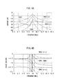
- FIG. 4A and FIG. 4B are diagrams for illustrating resonance frequency control in the wireless power transfer system depicted in FIG. 2 and FIG. 3 .
- an axis of abscissa represents the frequency f [MHz] of the AC power supply 11
- an axis of ordinates represents the magnitude [dB] of current I flowing in each coil.
- an axis of abscissa represents the frequency f [MHz] of the AC power supply 11
- an axis of ordinates represents the phase ⁇ [radian] of the current I flowing in each coil.
- the phase ⁇ represents the phase difference ⁇ from the phase ⁇ vs of the voltage Vs of the AC power supply 11, i.e., the phase difference ⁇ using the phase ⁇ vs of the voltage Vs supplied to the power supply coil 12 as a reference.
- the phase ⁇ is 0 when the phase ⁇ corresponds to the phase ⁇ vs.
- FIG. 4A and FIG. 4B illustrate a case of performing resonance frequency control, in which the power source resonance coil 13 or a set of the power source resonance coil 13 and the power receiver resonance coil 22 is controlled such that the resonance frequencies fs, fj are 10 MHz.
- the target value ⁇ ms is set to "- ⁇ radians (-180°)" in the target value setting unit 143, while the target value ⁇ mj is set to "-3 ⁇ /2 radians (-270°)" in the target value setting unit 143.
- the target value ⁇ mj is set to a value " ⁇ ms - ⁇ /2" obtained by adding - ⁇ /2 to the target value ⁇ ms, i.e., set to a phase being ⁇ /2 behind the target value ⁇ ms.
- the current Is of the power source resonance coil 13 peaks at 10 MHz which corresponds to the frequency fd of the AC power supply 11.
- the phase ⁇ is of the current Is of the power source resonance coil 13 is - ⁇ at 10 MHz which corresponds to the resonance frequency fs. In other words, the phase ⁇ is coincides with the target value ⁇ ms.
- the power source resonance coil 13 may be regarded as a serial resonance circuit when viewed from the power supply coil 12.
- a reactance is capacitive and becomes closer to - ⁇ /2, and at the higher frequency fd, the reactance is inductive and becomes closer to -3 ⁇ /2.
- the phase ⁇ is of the current Is flowing through the power source resonance coil 13 largely changes in the vicinity of the resonance frequency fs.
- the resonance frequency fs of the power source resonance coil 13 may be made to coincide with the frequency fd of the voltage Vs highly accurately by being controlled such that the phase ⁇ is, i.e., the phase difference ⁇ s is - ⁇ .
- the current I flowing in the power supply coil 12 also peaks at the resonance frequency fs.
- the phase ⁇ i of the current I flowing in the power supply coil 12 is 0 or a leading phase in the vicinity of the resonance frequency fs.
- the phase ⁇ i deviates from the resonance frequency fs, the phase ⁇ i becomes - ⁇ /2.
- the current Ij of the power receiver resonance coil 22 peaks at 10 MHz which coincides with the frequency fd of the AC power supply 11.
- the phase ⁇ ij of the current Ij of the power receiver resonance coil 22 is - 3 ⁇ /2 at 10 MHz which coincides with the resonance frequency fs. In other words, the phase ⁇ ij coincides with the target value ⁇ mj.
- the phase difference ⁇ decreases and is close to - ⁇ /2.
- the phase difference ⁇ increases and is close to -5 ⁇ /2, i.e., - ⁇ /2.
- the phases ⁇ is and ⁇ ij of the currents Is and Ij respectively flowing in the power source resonance coil 13 and the power receiver resonance coil 22 largely change in the vicinity of the resonance frequencies fs and fj, respectively.
- the resonance frequencies fs and fj of the power source resonance coil 13 and the power receiver resonance coil 22 may be made to highly accurately coincide with the frequency fd of the voltage Vs.
- the resonance frequencies of the Power source system coil SC and the Power receiver system coil JC may be made to accurately coincide with the frequency fd of the AC power supply 11. Power may constantly be transferred from the power source device 3 to the power receiver device 4 at maximum efficiency.
- control is performed, based on the phase difference ⁇ of the coil current with respect to the voltage Vs of the AC power supply.
- accurate control may be performed without influence of variation in the amplitude of the current, which affects control, e.g., when using a sweep search method.
- the sweep search method e.g., sweeping is performed on L or C in the Power source system coil SC or the Power receiver system coil JC.
- a position at which the current value of the coil is maximized (peaked) is searched for in a trial-and-error manner.
- FIG. 5A and FIG. 5B are diagrams for illustrating conditions for simulation in the wireless power transfer system depicted in FIG. 2 and FIG. 3 .
- the conditions for simulation are that the power supply coil 12 and the power source resonance coil 13 are coaxially arranged on a same plane, and that the power receiver resonance coil 22 and the power extraction coil 23 are also arranged coaxially on a same plane.
- the distance dd between the Power source system coil SC (the power supply coil 12 and the power source resonance coil 13) and the Power receiver system coil JC (the power receiver resonance coil 22 and the power extraction coil 23) is set at 25 mm.
- the drive frequency (the frequency fd of the AC power supply 11) is set at 7 MHz.
- the load (the resistance value of the load device 21) is set at 10 ⁇ .
- the thickness of each coil is set at ⁇ 0.5 mm.
- the outside diameter of the power supply coil 12 is set at ⁇ 30 mm.
- the number of turns of the power supply coil 12 is set at 1.
- the outside diameter of the power source resonance coil 13 is set at ⁇ 40 mm.
- the number of turns of the power source resonance coil 13 is set at 5.
- the outside diameter of the power receiver resonance coil 22 is set at ⁇ 30 mm.
- the number of turns of the power receiver resonance coil 22 is set at 5.
- the outside diameter of the power extraction coil 23 is set at ⁇ 20 mm.
- the number of turns of the power extraction coil 23 is set at 1.
- the distance (pitch) between the centers of adjacent windings of each of the power source resonance coil 13 and the power receiver resonance coil 22 is set at 0.8 mm.
- FIG. 6A and FIG. 6B are diagrams depicting a result of simulation in the wireless power transfer system depicted in FIG. 2 and FIG. 3 , which is performed under the conditions for simulation illustrated in FIG. 5A and FIG. 5B .
- the axis of ordinates represents the amplitude of a drive voltage, which is normalized (the maximum amplitude is set to "1").
- the axis of abscissas represents time normalized (1/7 MHz is set to "1").
- the reference sign ⁇ d represents phase delays of a power source side drive voltage LL1 and a power receiver side drive voltage LL2.
- the axis of ordinates represent a power transfer efficiency (the maximum efficiency is set to "1")
- the axis of abscissas represents a phase delay ⁇ d (deg: °).
- a power transfer efficiency decreases with increase of the phase delays ⁇ d of the power source side drive voltage LL1 and the power receiver side drive voltage LL2. Particularly, it is seen that when the phase delay ⁇ d exceeds 40°, the power transfer efficiency decreases largely.
- a delay time td corresponding to a phase delay of 1° is calculated as follows.
- the power transfer efficiency decreases even for a very short delay time td.
- the power source 1 and the power receiver 2 each have a communication circuit which transmits and receives information concerning the positions of the transmitter and the receiver, electric power to be transferred, and the like. It is difficult for these communication circuits to process data for phase control of a drive voltage of 7 MHz (generally, hundreds of KHz to tens of MHz).
- the power source 1 is equipped with a dedicated phase transmission unit 145.
- the power receiver 2 is equipped with a dedicated phase reception unit 241.
- the phase of a voltage waveform of the AC power supply 11, which is obtained in the power source 1, is accurately transferred to the power receiver 2 without delay.
- the dedicated phase transmission unit 145 and the dedicated phase reception unit 241 are provided in the power source 1 and the power receiver 2, respectively. Accordingly, hardware volume increases. Thus, cost increases.
- FIG. 7 is a block diagram depicting a wireless power transfer system according to a first embodiment.
- a power source side control unit 16 and a power source side communication unit 17 are provided in a power source 1, instead of the dedicated phase transmission unit 145.
- the wireless power transfer system is configured so that a power receiver side control unit 26, a power receiver side communication unit 27, and a power receiver side phase adjustment oscillation unit 28 are provided in the power receiver 2, instead of the dedicated phase reception unit 241.
- the wireless power transfer system according to the first embodiment does not need high-speed data transfer as needed in the wireless power transfer system, e.g., depicted in FIG. 3 . Therefore, the power source side communication unit 17 and the power receiver side communication unit 27 may act also as a communication circuit for transmitting and receiving information concerning the positions of the transmitter and the receiver, electric power to be transferred, and the like.
- the wireless power transfer system according to the first embodiment need not perform real-time phase control of a resonance frequency of, e.g., hundreds of KHz to tens of MHz.
- a communication circuit generally provided therein may be used without change.
- each of an AC power supply 11, a power supply coil 12, a power source resonance coil 13, a capacitor 132, a current detection sensor SE1, and a power source side feedback control unit 144, and the like of the power source 1 are substantially similar to those described with reference to FIG. 3 .
- each of a power receiver resonance coil 22, a power extraction coil 23, a capacitor 222, a current detection sensor SE2, and a power receiver side feedback control unit 244, and the like of the power receiver 2 are substantially similar to those described with reference to FIG. 3 .
- a target value ⁇ ms in the power source 1 is output from a target value setting unit 143.
- a target value ⁇ mj in the power receiver 2 is output from a target value setting unit 243.
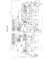
- FIG. 8 is a block diagram depicting a wireless power transfer system according to a second embodiment.
- FIG. 9 to FIG. 12 are diagrams for illustrating an operation in the wireless power transfer system depicted in FIG. 8 .
- FIG. 8 to FIG. 10 illustrate the system while focusing on the power source side control unit 16, the power source side communication unit 17, the AC power supply 11, the power supply coil 12, the power source resonance coil 13, the capacitor (variable capacity device) 132, and the power source side feedback control unit 144 in the power source 1.
- phase comparison unit (second phase comparison unit) 151 of the power source 1 is provided in the power source side feedback control unit 144.
- the phase comparison unit 151 and the power source side feedback control unit 144 are drawn separately from each other.
- FIG. 8 to FIG. 10 illustrate the system while focusing on a power receiver side control unit 26, a power receiver side communication unit 27, a power receiver side phase adjustment oscillation unit 28, the power receiver resonance coil 22, a power take-out unit 23, a capacitor 222, and a power receiver side feedback control unit 244 in the power receiver 2.
- phase comparison unit 251 of the power receiver 2 is provided in the power receiver side feedback control unit 244.
- the phase comparison unit 251 and the power receiver side feedback control unit 244 are drawn separately from each other.
- a rectification circuit 211 and a load device 21 having a load (e.g., a battery: a resistance value RL) 212, and a dummy load 29 having a resistance value RL' which is substantially equal to the resistance value RL of the load 212, are drawn together with switches SW1 to SW4.
- each of the power supply coil 12, the power source resonance coil 13, the power receiver resonance coil 22, and the power extraction coil 23 is drawn by depicting an equivalent circuit, using resistors R 1 , R 2 , R 13 , and R 4 , and inductors L 1 , L 2 , L 3 , and L 4 .
- Currents flowing in the power supply coil 12, the power source resonance coil 13, the power receiver resonance coil 22, and the power extraction coil 23 are designated as I 1 , I 2 , I 3 , and I 4 .
- a target value ⁇ ms in the power source 1 is output from the power source side control unit 16
- a target value ⁇ mj in the power receiver 2 is output from the power receiver side control unit 26.
- the wireless power transfer system according to the second embodiment is configured to be substantially similar to the wireless power transfer system according to the first embodiment, except that the power source 1 does not have a target value setting unit 143, and that the power receiver 2 does not have a target value setting unit 243.
- an operation of the wireless power transfer system according to the first embodiment differs only in places from which the target values ⁇ ms and ⁇ mj are output, and is similar to an operation of the wireless power transfer system according to the second embodiment which will be described below.
- each target value is output from the power source side control unit 16 and the power receiver side control unit 26. Consequently, each target value may be controlled as an optimal value for the wireless power transfer system to be used. Alternatively, each target value may be controlled by being changed to implement another function.
- the target value (target value of the phase difference ⁇ s) ⁇ ms for the power source side feedback control unit 144 is output from the power source side control unit 16.
- the AC power supply 11 is controlled by a control signal Sps output from the power source side control unit 16.
- the target value (target value of the phase difference ⁇ j) ⁇ mj for the power receiver side feedback control unit 244 is output from the power receiver side control unit 26.
- the power receiver side phase adjustment oscillation unit 28 is controlled by a control signal Spj output from the power receiver side control unit 26.
- the power receiver side phase adjustment oscillation unit 28 in the power receiver 2 outputs a signal (voltage VB) having a frequency to be used for power transfer, i.e., a fixed oscillating frequency being equal to that of the AC power supply 11 in the power source 1.
- the AC power supply 11 and the power receiver side phase adjustment oscillation unit 28 are controlled using, e.g., a crystal oscillator such that the oscillating frequencies thereof are accurately equal to each other.
- a switch SW1 is provided in the power receiver side resonance coil 22.
- a switch SW2 is provided between the power receiver side phase adjustment oscillation unit 28 and the power receiver resonance coil 22.
- a switch SW3 is provided between the power extraction coil 23 and the load device 21.
- a dummy load 29 is provided via a switch SW4 between both ends of the power extraction coil 23.
- the switches SW1 to SW4 are, e.g., n-channel type MOS transistors (nMOS transistors) each having a gate to which a control signal is applied.
- nMOS transistors n-channel type MOS transistors
- a control signal CSj output from the power receiver side control unit 26 is applied to the control terminal (gate of each nMOS transistor) of each of the switches SW1 and SW3.
- a control signal /CSj obtained by inverting the control signal CSj at an inverter is applied to the control terminal of each of the switches SW2 and SW4.
- the power receiver side phase adjustment oscillation unit 28 of the power receiver 2 is put into an operating state (i.e., turned on) by the control signal Spj output from the power receiver side control unit 26.
- the resistance value RL' of the dummy load 29 is set to be substantially equal to the resistance value RL of the load 212 of the load device 21.
- the target value ⁇ mj given to the power receiver side feedback control unit 244 from the power receiver side control unit 26 is set to, e.g., 0°.
- the output voltage VB from the power receiver side phase adjustment oscillation unit 28 is used to adjust the resonance frequency in the power receiver 2, and therefore, the power capacity of the voltage VB is minute.
- a rectification circuit (rectification IC) 211 of the load device 21 may not be operated by the voltage VB, and the resistance value RL of the load resistor 212 may not be accurately reflected due to non-linear characteristics.
- the dummy load 29 being comparable to the load resistor 212 is connected to the power extraction coil 23, instead of the actual load device 21.
- the adjustment of the resonance frequency of the power receiver 2 is made by the voltage VB corresponding to the minute power capacity.
- the power receiver side feedback control unit 244 controls the electrostatic capacity of the capacitor 222 via a control signal KSj to be a predetermined value such that the phase difference ⁇ j is equal to the target value ⁇ mj.
- the resonance frequency of the power source 1 is adjusted in a time Tcs.
- the resonance frequency of the power receiver 2 is adjusted in a time Tcj.
- the above adjustment of the resonance frequency in the power receiver 2 is performed in the latter half Tcj of the time in which resonance adjustment processing is performed.
- the adjustment of the resonance frequency in the power source 1 is performed.
- the AC power supply 11 of the power source 1 is put into a low output state (adjustment output state) by a control signal Sps output from the power source side control unit 16.
- the AC power supply 11 In the low output state of the AC power supply 11, the AC power supply 11 does not output a voltage for transferring power to the power receiver 2. The AC power supply 11 simply outputs a low voltage for adjusting the resonance frequency in the power source 1.
- the feedback control is such that, as described with reference to FIG. 2 to FIG. 4B , e.g., the power source side feedback control unit 144 controls the electrostatic capacity of the capacitor 132 via a control signal KSs to a predetermined value so that the phase difference ⁇ s is equal to the target value ⁇ ms.
- the adjustment of the resonance frequency in the power source 1 is not necessarily performed immediately before the adjustment of the resonance frequency in the power receiver 2.
- the adjustment of the resonance frequency in the power source 1 may be performed simultaneously with or immediately after the adjustment of the resonance frequency in the power receiver 2, or alternatively, at another appropriate timing.
- the power receiver side phase adjustment oscillation unit 28 of the power receiver 2 is put into a stopped state (off-state) by the control signal Spj output from the power receiver side control unit 26.
- the switch SW2 is turned off, the power receiver side phase adjustment oscillation unit 28 is disconnected from the power receiver resonance coil 22.
- the power receiver resonance coil 22 receives power from the power source resonance coil 13 in the power source 1 by magnetic field resonance (magnetic field resonating). At that time, the power extraction coil 23 is connected to the load device 21 by the turn-on of the switch SW3 and the turn-off of the switch SW4.
- the AC power supply 11 is put into an operating state (which is not a low power operating state, and is a normal operating state) by a control signal Sps output from the power source side control unit 16.
- the resonance frequency of the power source resonance coil 13 in the power source 1 is controlled so as to coincide with the frequency of the AC power supply 11 in the time Tcs.
- the resonance frequency of the power receiver resonance coil 22 in the power receiver 2 is controlled so as to coincide with the frequency of the power receiver side phase adjustment oscillation unit 28.
- the frequency of the AC power supply 11 and the frequency of the power receiver side phase adjustment oscillation unit 28 are accurately controlled using, e.g., a crystal oscillator.
- the power transfer by the magnetic field resonance from the power source 1 to the power receiver 2, in both of which the resonance frequencies are adjusted, may be performed with high power transfer efficiency.
- the resonance frequency adjustment times (Tcs, Tcj: resonance adjustment) in the power source 1 and the power receiver 2 are repeated at predetermined intervals.
- the intervals for repeating the resonance adjustment may variously be set according to the number of the power source 1 and the power receiver 2, the power capacity thereof, or the surrounding environment thereof, or the like. For example, a several-minute interval may be set as the interval for repeating the resonance adjustment.
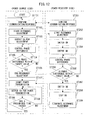
- steps ST101 and ST201 e.g., it is checked whether the power receiver 2 is present within a range in which power may be transferred by the power source 1 to the power receiver 2.
- the transfer of information concerning the position and the inclination of the power receiver 2, and electric power to be transmitted, and the authentication of the power receiver 2 in a paid power transfer system are performed.
- step ST102 the processing proceeds to step ST102, whereupon the adjustment (resonance adjustment) of the resonance frequency in the power source 1 is started, which has been described with reference to the time Tcs depicted in FIG. 9 and FIG. 11 .
- step ST103 the output voltage VA of the AC power supply 11 is set to the adjustment output voltage (low output voltage).
- step ST104 the phase difference is controlled.
- step ST104 phase difference control processing is performed by the power source side feedback control unit 144.
- step ST105 the phase difference control processing in step ST104 is repeated until the phase difference ⁇ s becomes less than the target value ⁇ ms.
- step ST105 if it is determined in step ST105 that the phase difference ⁇ s is within a range prescribed by the target value ⁇ ms, the processing proceeds to step ST106 in which the resonance adjustment processing by the power source 1 is terminated. Then, the processing proceeds to step ST107.
- step ST202 when the resonance frequency adjustment processing by the power source 1 is terminated in the time Tcs, in step ST202, on the power receiver side, the adjustment of the resonance frequency (resonance adjustment) in the power receiver 2 is started in a time Tcj subsequent to the time Tcs.
- the power receiver 2 recognizes the termination of the resonance frequency adjustment processing in the power source 1 by the communication between the power source side communication unit 17 and the power receiver side communication unit 27.
- the resonance adjustment is started by the power receiver 2.
- step ST203 the switching of the switches SW1 to SW4 described with reference to FIG. 9 is performed. Then, the processing proceeds to step ST204 in which the power receiver side phase adjustment oscillation unit 28 is put into an operating state (in which the voltage VB is output) by the power receiver side control unit 26.
- the switches SW1 and SW3 are turned off.
- the switches SW2 and SW4 are turned on.
- the output voltage VB of the power receiver side phase adjustment oscillation unit 28 is applied to both ends of the power receiver resonance coil 22.
- the load device 21 is disconnected from the power extraction coil 23, and instead, the dummy load 29 is connected to the power extraction coil 23.
- step ST205 the processing proceeds to step ST205 in which phase difference control processing is performed by the power receiver side feedback control unit 244.
- step ST206 the phase difference control processing in step ST205 is repeated until the phase difference ⁇ j becomes less than the target value ⁇ mj.
- step ST206 determines whether the phase difference ⁇ j is within a range prescribed by the target value ⁇ mj. If it is determined in step ST206 that the phase difference ⁇ j is within a range prescribed by the target value ⁇ mj, the processing proceeds to step ST207 in which the switching of the switches SW1 to SW4 described with reference to FIG. 10 is performed. Then, the processing proceeds to step ST208.
- step ST208 the power receiver side phase adjustment oscillation unit 28 is put into a stopped state (the output voltage VB is stopped) by the power receiver side control unit 26. Then, the processing proceeds to step ST209 in which the resonance adjustment processing in the power receiver 2 is terminated.
- the power receiver side control unit 26 notifies the power source side of the termination of the resonance adjustment processing.
- the power source 1 recognizes the termination of the resonance frequency adjustment processing in the power receiver 2 by the communication between the power source side communication unit 17 and the power receiver side communication unit 27.
- step ST107 power transmission is started by the power source 1.
- step ST108 the AC power supply 11 is put into a normal operating state by the control signal Sps output from the power source side control unit 16, instead of being put into a low power operating state.
- the AC power supply 11 outputs a power transmission output voltage VB.
- both of the power source 1 and the power receiver 2 are put into a state in which the resonance frequency adjustment is completed. In this state, power transfer by magnetic field resonance from the power source 1 to the power receiver 2 is performed. Thus, power transfer with high power transfer efficiency is made possible.
- step ST109 If it is determined in step ST109 that a prescribed time has passed, the processing returns to step ST101 (ST201). Then, similar processing is repeated. In other words, the adjustment of the resonance frequency in the power source 1 and the power receiver 2 is repeated at predetermined intervals.
- step ST103 the output voltage VA of the AC power supply 11 is set to a low output voltage for adjustment.
- both of the adjustment of the resonance frequency in the power source 1 and the adjustment of the resonance frequency in the power receiver 2 may be performed in parallel.
- the adjustment of the resonance frequency in the power source 1 is not necessarily performed immediately before the adjustment of the resonance frequency in the power receiver 2.
- the adjustment of the resonance frequency in the power source 1 may be performed simultaneously with or immediately after the adjustment of the resonance frequency in the power receiver 2, or alternatively, at another appropriate timing.
- the power source it is not necessary for the power source to transmit the phase of the voltage waveform of the AC power supply accurately without delay to the power receiver.
- a dedicated communication circuit capable of performing high-speed data transfer is unnecessary.
- the hardware volume may be reduced.
- the cost may be decreased.
- FIG. 13 is a block diagram depicting a wireless power transfer system according to the third embodiment.
- FIG. 14 and FIG. 15 are diagrams for illustrating an operation of the wireless power transfer system depicted in FIG. 13 .
- a power source 1 includes a temperature sensor (second temperature sensor) 100.
- the power receiver 2 includes a temperature sensor (first temperature sensor) 200.
- the temperature sensor 100 measures (detects) the temperature of each of a power supply coil 12 and a power source resonance coil 13 in the power source 1, and outputs a temperature signal (second temperature signal) Tss to a power source side control unit 16.
- the temperature sensor 200 measures the temperature of each of a power receiver resonance coil 22 and a power extraction coil 23 in the power receiver 2, and outputs a temperature signal (first temperature signal) Tsj to a power receiver side control unit 26.
- the temperature sensor 100 has only to measure the temperature of the power source resonance coil 13.
- the temperature sensor 200 has only to measure the temperature of the power receiver resonance coil 22.
- a power supply time (time Tps) and a resonance adjustment time (times Tcs and Tcj) are substantially the same as those depicted in FIG. 11 .
- time Tps time
- Tcs and Tcj resonance adjustment time
- steps ST101 to ST108 on the power source side power source 1
- steps ST201 to ST209 on the power receiver side power receiver 2
- steps ST101 to ST108 on the power source side power source 1
- steps ST201 to ST209 on the power receiver side power receiver 2
- step ST209 on the power receiver side resonance adjustment processing in the power receiver 2 is terminated.
- the power source side is notified of the termination of the resonance adjustment processing.
- step ST210 on the power receiver side the processing proceeds to step ST210 on the power receiver side.
- step ST210 on the power receiver side it is determined whether the temperature sensor 200 provided in the power receiver 2 detects an abnormality, i.e., whether temperature signals Tsj by the temperature sensor 200 representing the temperature of the power receiver resonance coil 22 and the temperature of the power extraction coil 23 indicate abnormal values. If it is determined in step ST210 that the temperature sensor 200 does not detect an abnormality, power transfer from the power source 1 to the power receiver 2 is continued in an unchanged state.
- step ST210 if it is determined in step ST210 that the temperature sensor 200 detects an abnormality, i.e., the temperature signal Tsj exceeds a threshold temperature Tha indicating an abnormality, the processing proceeds to step ST211 in which the detection of an abnormality by the temperature sensor 200 is transmitted to the power receiver side.
- the detection of an abnormality in step ST211 on the power receiver side is transmitted to the power receiver side.
- step ST110 the detection of the abnormality is processed as the power transmitting/receiving temperature monitoring.
- step ST212 it is determined whether the power receiver side temperature sensor 200 detects a normal value. If it is determined in step ST212 that the power receiver side temperature sensor 200 does not detect a normal value, the power receiver 2 maintains the state without change and waits for the detection of a normal value by the power receiver side temperature sensor 200.
- a power transmission output voltage VA is stopped by performing processing in step ST112 on the power source side, as will be described below.
- the power transfer is stopped.
- the level of the temperature signal Tsj output from the power receiver side temperature sensor 200 is lowered with time.
- step ST212 If it is determined in step ST212 on the power receiver side that the power receiver side temperature sensor 200 detects a normal value, the processing proceeds to step ST213 in which the power source side is notified of the detection of a normal value by the power receiver side temperature sensor 200. Then, the processing returns to step ST210 in which similar processing is performed.
- step ST108 on the power source side the AC power supply 11 outputs a power transmission output voltage VB for performing a usual power transmission operation. Then, the processing proceeds to step ST110 in which power transmitting/receiving temperature monitoring is performed.
- the power transmitting/receiving temperature monitoring in step ST110 includes the monitoring of the temperature of each of the power supply coil 12 and the power source resonance coil 13 by the temperature sensor 100 of the power source 1, and the monitoring of the temperature of each of the power receiver resonance coil 22 and the power extraction coil 23 by the temperature sensor 200 of the power receiver 2.
- the temperature signal Tss detected by the power source side temperature sensor 100 is input to the power source side control unit 16 without change.
- the temperature signal Tsj detected by the power receiver side temperature sensor 200 is transmitted to the power source side control unit 16 via communication (communication units 17, 27, and the like).
- step ST111 it is determined whether the power source side temperature sensor 100 or the power receiver side temperature sensor 200 detects an abnormality. If it is determined that both of the sensors do not detect an abnormality, the power transfer from the power source 1 to the power receiver 2 is continued while performing the power transmitting/receiving temperature monitoring.
- step ST111 if it is determined in step ST111 that at least one of the power source side temperature sensor 100 or the power receiver side temperature sensor 200 detects an abnormality, the processing proceeds to step ST112 in which the output voltage VA for power transmission is stopped.
- the power source side control unit 16 stops an operation of the AC power supply 11 by a control signal Sps.
- step ST112 If the output voltage VB for power transmission is stopped in step ST112, then, the processing proceeds to step ST113 in which the power transmitting/receiving temperature monitoring is performed again.
- step ST114 it is determined whether both of the power source side temperature sensor 100 and the power receiver side temperature sensor 200 detect a normal value. If it is determined that at least one of the power source side temperature sensor 100 and the power receiver side temperature sensor 200 detects an abnormality, the power source 1 continues to stop the output voltage VB for power transmission, while performing power transmitting/receiving temperature monitoring.
- step ST114 it is determined in step ST114 that both of the power source side temperature sensor 100 and the power receiver side temperature sensor 200 detect normal values, the processing returns to step ST101 (ST201).
- target value setting units 143 and 243 may be provided in the power source 1 and the power receiver 2, respectively, to output target values ⁇ ms and ⁇ mj.
- the number of the power sources 1 and that of the power receivers 2 are 1. It is apparent that the number of the power sources 1 and that of the power receivers 2 each may be plural.
- the power transfer from the power source resonance coil (LC resonator) 13 to the power receiver resonance coil (LC resonator) 22 is not limited to that using a magnetic field resonance (magnetic field resonating).
- the power transfer may use, e.g., an electric field resonance (electric field resonating).
Landscapes
- Engineering & Computer Science (AREA)
- Computer Networks & Wireless Communication (AREA)
- Power Engineering (AREA)
- Signal Processing (AREA)
- Charge And Discharge Circuits For Batteries Or The Like (AREA)
Abstract
Description
- Embodiments discussed herein relate to a wireless power transfer system, a power receiver and a wireless power transfer method.
- Recently, wireless power transfer techniques for power supply and electrification have attracted attention. Research and development have been conducted on wireless power transfer systems wirelessly transferring power to, e.g., various electronic devices such as mobile terminals and notebook computers, electrical household appliances or power infrastructure equipment.
- Generally, techniques using electromagnetic induction, and techniques using radio waves are known as this kind of wireless power transmission (wireless power transfer). On the other hand, recently, there have been expectations for power transfer techniques using magnetic field resonance and electric field resonance as techniques being capable of transferring power to a plurality of power receivers while placing each power receiver at a certain distance from a power source, or to various three-dimensional positions of each power receiver.
- Conventionally, various wireless power transfer techniques using magnetic field resonance have been proposed.
-
- Patent Document 1: International Publication Pamphlet No.
WO2011/099071 - Patent Document 2: Japanese Laid-open Patent Publication No.
2010-148174 - As described above, conventionally, wireless power transfer techniques for wirelessly transferring power for power supply and electrification have been widely used. However, e.g., when there is a difference in resonance frequency between a power source and a power receiver, transfer efficiency is degraded. Thus, real-time phase control may be important so as to prevent degradation of the transfer efficiency.
- However, the resonance frequency in the wireless power transfer system is, e.g., from hundreds of KHz to tens of MHz. Thus, in order to perform real-time phase control, dedicated communication circuits are provided to the power source and the power receiver, respectively. Accordingly, hardware volume on each of the power source and the power receiver increases. Thus, cost increases.
- According to one embodiment, a power receiver is provided, which includes a power receiver resonance coil that wirelessly receives power from a power source using a magnetic field resonance or electric field resonance, a power receiver side communication unit, and a power receiver side control unit.
- The power receiver side phase adjustment oscillation unit outputs a voltage oscillating at a predetermined frequency. The power receiver side communication unit communicates with the power source. The power receiver side control unit receives an output from the power receiver side communication unit and adjusts the resonance frequency of the power receiver resonance coil using an output voltage from the power receiver side phase adjustment oscillation unit.
- The wireless power transfer system, the power receiver and the wireless power transfer method disclosed have an advantageous effect in that the power transfer efficiency may be enhanced while suppressing increase in the hardware volume and cost.
-
- [
FIG. 1] FIG. 1 is a diagram schematically depicting a wireless power transfer system. - [
FIG. 2] FIG. 2 is a block diagram depicting one example of a wireless power transfer system. - [
FIG. 3] FIG. 3 is a block diagram depicting the wireless power transfer system depicted inFIG. 2 while focusing on a control system. - [
FIG. 4A] FIG. 4A is a diagram (1) for illustrating resonance frequency control in the wireless power transfer system depicted inFIG. 2 andFIG. 3 . - [
FIG. 4B] FIG. 4B is a diagram (2) for illustrating resonance frequency control in the wireless power transfer system depicted inFIG. 2 andFIG. 3 . - [
FIG. 5A] FIG. 5A is a diagram (1) for illustrating conditions for simulation in the wireless power transfer system depicted inFIG. 2 andFIG. 3 . - [
FIG. 5B] FIG. 5B is a diagram (2) for illustrating conditions for simulation in the wireless power transfer system depicted inFIG. 2 andFIG. 3 . - [
FIG. 6A] FIG. 6A is a diagram (1) depicting a result of simulation in the wireless power transfer system depicted inFIG. 2 andFIG. 3 , which is performed under the conditions for simulation illustrated inFIG. 5A and FIG. 5B . - [
FIG. 6B] FIG. 6B is a diagram (2) depicting a result of simulation in the wireless power transfer system depicted inFIG. 2 andFIG. 3 , which is performed under the conditions for simulation illustrated inFIG. 5A and FIG. 5B . - [
FIG. 7] FIG. 7 is a block diagram depicting a wireless power transfer system according to a first embodiment. - [
FIG. 8] FIG. 8 is a block diagram depicting a wireless power transfer system according to a second embodiment. - [
FIG. 9] FIG. 9 is a diagram (1) for illustrating an operation of the wireless power transfer system depicted inFIG. 8 . - [
FIG. 10] FIG. 10 is a diagram (2) for illustrating an operation of the wireless power transfer system depicted inFIG. 8 . - [
FIG. 11] FIG. 11 is a diagram (3) for illustrating an operation of the wireless power transfer system depicted inFIG. 8 . - [
FIG. 12] FIG. 12 is a diagram (4) for illustrating an operation of the wireless power transfer system depicted inFIG. 8 . - [
FIG. 13] FIG. 13 is a block diagram depicting a wireless power transfer system according to a third embodiment. - [
FIG. 14] FIG. 14 is a diagram (1) for illustrating an operation of the wireless power transfer system depicted inFIG. 13 . - [
FIG. 15] FIG. 15 is a diagram (2) for illustrating an operation of the wireless power transfer system depicted inFIG. 13 . - First, before describing embodiments of the wireless power transmission (wireless power transfer) system, the power receiver, and the wireless power transfer method in detail, an example of the wireless power transfer system and problems thereof are described with reference to
FIG. 1 to FIG. 6B . -
FIG. 1 is a diagram schematically depicting a wireless power transfer system. As depicted inFIG. 1 , the wireless power transfer system has a primary side (power source side: a power source) 1 and a secondary side (power receiver side: a power receiver) 2. Thepower source 1 and thepower receiver 2 may be plural. - The
power source 1 includes anAC power supply 11, and a Power source system coil SC including apower supply coil 12 and a powersource resonance coil 13. Thepower receiver 2 includes a Power receiver system coil JC including a powerreceiver resonance coil 22 and apower extraction coil 23, and aload device 21. - As depicted in
FIG. 1 , thepower source 1 and thepower receiver 2 transfer energy (electric-power) from thepower source 1 to thepower receiver 2 by magnetic field resonance (magnetic field resonating) between the power source resonance coil (LC resonator) 13 and the power receiver resonance coil (LC resonator) 22. The transfer of power from theLC resonator 13 to theLC resonator 22 may be performed using electric field resonance (electric field resonating) or the like. However, in the following description, the case of using the magnetic field resonance will mainly be described as an example. - In the Power source system coil SC, the power transfer from the
power supply coil 12 to the powersource resonance coil 13 is performed using electromagnetic induction. In the Power receiver system coil JC, the power transfer from the powerreceiver resonance coil 22 to thepower extraction coil 23 is also performed using electromagnetic induction. -
FIG. 2 is a block diagram depicting an example of the wireless power transfer system and illustrates in more detail the wire power transfer system depicted inFIG. 1 . As depicted inFIG. 2 , the power transfer system includes the Power source system coil SC, the Power receiver system coil JC, theAC power supply 11, a power sourceside control circuit 14, thedevice 21 serving as a load, and a power receiverside control circuit 24. - As described above, the Power source system coil SC includes the
power supply coil 12 and the powersource resonance coil 13. Thepower supply coil 12 is windings obtained by circumferentially winding a metal wire, e.g., a copper wire or an aluminum wire a plurality of times. An AC voltage (high-frequency voltage) generated by theAC power supply 11 is applied to both ends thereof. - The power
source resonance coil 13 includes acoil 131 obtained by circumferentially winding a metal wire, e.g., a copper wire or an aluminum wire, and acapacitor 132 connected to both ends of thecoil 131 so as to form a resonance circuit configured by this coil and this capacitor. A resonance frequency f0 is expressed by the following expression.
where L is the inductance of thecoil 131, and C is the capacitance of thecapacitor 132. - The
coil 131 of the powersource resonance coil 13 is, e.g., a one-turn coil. Various types of capacitors may be used as thecapacitor 132. However, a capacitor with a minimized loss and a sufficient pressure resistance is preferable. - In the wireless power transfer system depicted in
FIG. 2 , in order to make the resonance frequency variable, a variable capacitor is used as thecapacitor 132. For example, a variable capacity device manufactured using MEMS technology, and a variable capacity device (varactor) using a semiconductor may be applied to the variable capacitor. - The
power supply coil 12 and the powersource resonance coil 13 are arranged to be coupled electromagnetically and closely to each other. For example, these coils are concentrically arranged on a same plane. In other words, these coils are arranged in a state in which thepower supply coil 12 is provided inside the powersource resonance coil 13. Alternatively, the powersource resonance coil 13 and thepower supply coil 12 may be coaxially arranged with an appropriate distance from each other. - When an AC voltage is applied from the
AC power supply 11 to thepower supply coil 12 in this state, a resonance current flows in the powersource resonance coil 13 by electromagnetic induction due to an alternating magnetic field generated in thepower supply coil 12. In other words, electric power is transferred from thepower supply coil 12 to the powersource resonance coil 13 by electromagnetic induction. - The Power receiver system coil JC includes the power
receiver resonance coil 22 and thepower extraction coil 23. The powerreceiver resonance coil 22 includes acoil 221 formed by winding a metal wire such as a copper wire or an aluminum wire circumferentially, and acapacitor 222 connected to both ends of thecoil 221. The resonance frequency f0 of the powerreceiver resonance coil 22 is expressed by the above expression (1) according to the inductance of thecoil 221 and the capacity of thecapacitor 222. - The
coil 221 of the powerreceiver resonance coil 22 is, e.g., a one-turn coil. Various types of capacitors may be applied to thecapacitor 222, as described above. In this wireless power transfer system depicted inFIG. 2 , in order to make the resonance frequency variable, a variable capacitor is used as thecapacitor 222. - Similarly to the
capacitor 132, a variable capacity device manufactured using, e.g., MEMS technology, or a varactor may be applied to the variable capacitor. - The
power extraction coil 23 is a winding obtained by circumferentially winding a metal wire, e.g., a copper wire or an aluminum wire a plurality of times. Thedevice 21 serving as a load is connected to both ends of thecoil 23. Theload device 21 is, e.g., a battery used as a power supply for thepower receiver 2 or a circuit for charging the battery. - The power
receiver resonance coil 22 and thepower extraction coil 23 are arranged to be coupled electromagnetically and closely to each other. For example, these coils are concentrically arranged on a same plane. In other words, these coils are arranged in a state in which thepower extraction coil 23 is provided inside the powerreceiver resonance coil 22. Alternatively, the powerreceiver resonance coil 22 and thepower extraction coil 23 may be coaxially arranged with an appropriate distance from each other. - When a resonance current flows in the power
receiver resonance coil 22 in this state, a current flows in thepower extraction coil 23 by electromagnetic induction due to an alternating magnetic field generated by the resonance current. In other words, electric power is transferred from the powerreceiver resonance coil 22 to thepower extraction coil 23 by electromagnetic induction. - Electric power is wirelessly transferred by the magnetic field resonance from the Power source system coil SC to the Power receiver system coil JC. Thus, as depicted in
FIG. 2 , the Power source system coil SC and the Power receiver system coil JC are arranged within a range of an appropriate distance from each other such that the coil planes of these coils are parallel to each other and that the coil axis centers of these coils coincide with each other or are not largely shifted from each other. - As depicted in
FIG. 2 , in a power transfer system, a direction along the coil axis center KS is a main radiation direction of a magnetic field KK, and a direction from the Power source system coil SC to the Power receiver system coil JC is a power transmitting direction SH. - When both of the resonance frequency fs of the power
source resonance coil 13 and the resonance frequency fj of the powerreceiver resonance coil 22 coincide with the frequency fd of theAC power supply 11, the maximum power is transferred. - However, if these resonance frequencies fs and fj are shifted from each other, or deviate from the frequency fd of the
AC power supply 11, the transferred power decreases, and the efficiency of power transfer decreases. - Therefore, in the power transfer system depicted in
FIG. 2 , resonance frequency control is performed by the power sourceside control circuit 14 and the power receiverside control circuit 24, using the phase φvs of theAC power supply 11 and the phases φis and φij of currents respectively flowing in the powersource resonance coil 13 and the powerreceiver resonance coil 22. - The power source
side control circuit 14 detects the phase φvs of the voltage Vs applied to the Power source system coil SC and the phase φis of the current Is flowing in the Power source system coil SC, and performs variable control of the resonance frequency fs of the Power source system coil SC such that the phase difference Δφs therebetween becomes a predetermined target value φms. - In other words, the power source
side control circuit 14 has a current detection sensor SE1, aphase detection units value setting unit 143, a power source sidefeedback control unit 144, and aphase transmission unit 145. - The current detection sensor SE1 detects the current Is flowing in the power
source resonance coil 13. For example, a hall effect element, a magnetic resistance element or a detection coil or the like may be used as the current detection sensor SE1. The current detection sensor SE1 outputs a voltage signal according to, e.g., the waveform of the current Is. - The
phase detection unit 141 detects the phase φvs of the voltage Vs applied to thepower supply coil 12, and outputs a voltage signal according to, e.g., the waveform of the voltage Vs. Thephase detection unit 141 may output the voltage Vs without any changes, or by dividing the voltage Vs by an appropriate resistor. Thus, thephase detection unit 141 may be configured by a simple electric wire, or by one or more resistor elements. - The
phase detection unit 142 detects the phase φis of a current Is flowing in the powersource resonance coil 13, based on an output from the current detection sensor SE1, and outputs a voltage signal according to, e.g., the waveform of the current Is. Thephase detection unit 142 may output the output of the current detection sensor SE1 without any change. Thus, the current detection sensor SE1 may serve also as thephase detection unit 142. - The target
value setting unit 143 sets and stores the target value φms of the phase difference Δφs. Therefore, a memory for storing the target value φms is provided in the targetvalue setting unit 143. For example, "-180°(-π radians)" or "a value obtained by adding an appropriate correction value a to -180°" is set as the target value φms. - The target value φms may be set by selecting from one or more data preliminarily stored, or may be set according to a command from a CPU, a keyboard, or the like.
- The power source side
feedback control unit 144 performs variable control of the resonance frequency fs of the powersource resonance coil 13 such that the phase difference Δφs between the phase φvs of the voltage Vs of theAC power supply 11 and the phase φis of the current Is of the powersource resonance coil 13 is the set target value φms. - The
phase transmission unit 145 wirelessly transmits information concerning the phase φvs of the voltage Vs supplied to thepower supply coil 12 to the power receiverside control circuit 24 as an analog signal or a digital signal. Thephase transmission unit 145 may transmit a signal obtained by, e.g., multiplying a voltage signal set according to the waveform of the voltage Vs by an integer in order to improve an S/N ratio. - The power receiver
side control circuit 24 detects the phase φvs of the voltage VS supplied to the Power source system coil SC and the phase φij of the current IJ flowing in the Power receiver system coil JC, and performs variable control of the resonance frequency fj of the Power receiver system coil JC such that the phase difference Δφj therebetween is a predetermined target value φmj. - The power source
side control circuit 24, a current detection sensor SE2, aphase reception unit 241, a phase detection unit 242, a targetvalue setting unit 243, and a power receiver sidefeedback control unit 244. - The current detection sensor SE2 detects the current Ij flowing in the power
receiver resonance coil 22. For example, a Hall device, a magnetic resistance element, or a detection coil or the like may be used as the current detection sensor SE2. The current detection sensor SE2 outputs a voltage signal according to, e.g., the waveform of the current Ij. - The
phase reception unit 241 receives and outputs information concerning the phase φvs transmitted from thephase transmission unit 145. If the voltage signal is multiplied at thephase transmission unit 145, frequency division is performed to demultiply the voltage signal at thephase reception unit 241. Thephase reception unit 241 outputs a voltage signal according to, e.g., the voltage Vs. - The phase detection unit 242 detects the phase φij of the current Ij flowing in the power
receiver resonance coil 22, based on the output from the current detection sensor SE2. The phase detection unit 242 outputs a voltage signal according to, e.g., the waveform of the current Ij. The phase detection unit 242 may output the output of the current detection sensor SE2 without any change. Thus, the current detection sensor SE2 may be configured to act also as the phase detection unit 242. - The target
value setting unit 243 sets and stores the target value φmj of the phase difference Δφj. Thus, a memory for storing the target value φmj is provided in the targetvalue setting unit 243. A value obtained by adding "-90° (-π/2 radians)" to the target value φms in the power sourceside control circuit 14 is set as the target value φmj. - In other words, e.g., "-270° (-3π/2 radians)" or "a value obtained by adding an appropriate value a to -270°", or the like is set as the target value φmj. A method for setting the target value φmj, and the like are similar to those used when setting the target value φms.
- The power receiver side
feedback control unit 244 performs variable control of the resonance frequency fj of the powerreceiver resonance coil 22 such that the phase difference Δφj between the phase φvs of the voltage Vs of theAC power supply 11 and the phase φij of the current Ij of the powerreceiver resonance coil 22 is the target value φmj. - The respective of the target
value setting unit 143 and the power source sidefeedback control unit 144 in the power sourceside control circuit 14, and the targetvalue setting unit 243 and the power receiver sidefeedback control unit 244 in the power receiverside control circuit 24 are simple examples of the resonance frequency control unit. -
FIG. 3 is a block diagram depicting the wireless power transfer system depicted inFIG. 2 while focusing on a control system.FIG. 3 illustrates in detail the power source sidefeedback control unit 144 of thepower source 1 and the power receiver sidefeedback control unit 244 of thepower receiver 2. - In the block diagram depicted as
FIG. 3 , for simplification, thephase detection units FIG. 2 are omitted. In other words, inFIG. 3 , the phase φis of the current Is flowing from the current detection sensor SE1 to the powersource resonance coil 13 is directly output. However, the phase φis may be output via, e.g., thephase detection unit 142 provided in the power source sidefeedback control unit 144. - As depicted in
FIG. 3 , the power source sidefeedback control unit 144 has aphase comparison unit 151, anaddition unit 152,gain adjustment units compensation unit 155, adriver 156, apolarity inversion unit 157, and the like. - The
phase comparison unit 151 compares the φis of the current Is detected by the current detection sensor SE1 and the phase φvs of the voltage Vs of theAC power supply 11, and outputs the phase difference Δφs therebetween. - The
addition unit 152 subtracts (inverts and adds) the target value φms set by the targetvalue setting unit 143 from the phase difference Δφs output by thephase comparison unit 151. Accordingly, when the phase difference Δφs and the target value φms are matched, an output of theaddition unit 152 is 0. - The output of the
addition unit 152 is inverted in polarity by thepolarity inversion unit 157, and next input to thegain adjustment unit 154, and then input to thecompensation unit 155. Thegain adjustment units - The
compensation unit 155 determines a gain corresponding to, e.g., a low frequency component. In other words, the power source sidefeedback control unit 144 may be regarded as a servo system performing feedback control on, e.g., an MEMS variable capacity device which is acapacitor 132. - Thus, an appropriate servo filter for stabilization, speeding-up, and improvement in accuracy of the servo system may be used as the
compensation unit 155. In addition, a filter circuit or a differentiation/integration circuit or the like for performing a PID (Proportional Integral Derivative Controller) operation in such a servo system is appropriately used. - The
driver 156 outputs a control signal KSs to, e.g., an MEMS variable capacity device which is acapacitor 132, and performs variable control of the capacitance of the MEMS variable capacity device. - The MEMS variable capacity device (MEMS variable capacitor) is configured to change electrostatic capacitance by providing, e.g., a lower electrode and an upper electrode on a glass substrate, and using change of a space due to flexure caused by an electrostatic attraction force which is generated by a voltage applied between the electrodes.
- The MEMS variable capacity device (capacitor 132) may be configured such that an electrode for the capacitor, and an electrode for driving may be provided separately from each other. The relationship between a voltage applied to the electrode for driving and an amount of the capacitance change is not linear. Thus, a calculation for the conversion, or table conversion is performed appropriately in, e.g., the
driver 156. - The power receiver side
feedback control unit 244 includes aphase comparison unit 251, anaddition unit 252,gain adjustment units compensation unit 255, adriver 256, and apolarity inversion unit 257. - An operation of each unit of the power receiver side
feedback control unit 244 is similar to that of each unit of the power source sidefeedback control unit 144. Therefore, description of the operation of each unit of the power receiver sidefeedback control unit 244 is omitted. - The power source
side control circuit 14 and the power receiverside control circuit 24 depicted inFIG. 2 , and the power source sidefeedback control unit 144 and the power receiver sidefeedback control unit 244 depicted inFIG. 3 , and the like may be implemented by software, or hardware, or a combination thereof. - Such control circuits and control units may be implemented using a computer including, e.g., a CPU, memories such as a ROM and a RAM, and other peripheral devices, and causing the CPU to execute appropriate computer programs. In that case, appropriate hardware circuits are combined with the computer.
-
FIG. 4A and FIG. 4B are diagrams for illustrating resonance frequency control in the wireless power transfer system depicted inFIG. 2 andFIG. 3 . InFIG. 4A , an axis of abscissa represents the frequency f [MHz] of theAC power supply 11, and an axis of ordinates represents the magnitude [dB] of current I flowing in each coil. InFIG. 4B , an axis of abscissa represents the frequency f [MHz] of theAC power supply 11, and an axis of ordinates represents the phase φ [radian] of the current I flowing in each coil. - The phase φ represents the phase difference Δφ from the phase φvs of the voltage Vs of the
AC power supply 11, i.e., the phase difference Δφ using the phase φvs of the voltage Vs supplied to thepower supply coil 12 as a reference. In other words, the phase φ is 0 when the phase φ corresponds to the phase φvs. - In reference signs CBA1 to CBA4 and CBB1 to CBB4 respectively designating curves, the
last numbers power supply coil 12, the powersource resonance coil 13, the powerreceiver resonance coil 22, thepower extraction coil 23, respectively. - In addition,
FIG. 4A and FIG. 4B illustrate a case of performing resonance frequency control, in which the powersource resonance coil 13 or a set of the powersource resonance coil 13 and the powerreceiver resonance coil 22 is controlled such that the resonance frequencies fs, fj are 10 MHz. - At that time, the target value φms is set to "-π radians (-180°)" in the target
value setting unit 143, while the target value φmj is set to "-3π/2 radians (-270°)" in the targetvalue setting unit 143. - In other words, the target value φmj is set to a value "φms - π/2" obtained by adding -π/2 to the target value φms, i.e., set to a phase being π/2 behind the target value φms.
- As indicated by the curve CBA2, the current Is of the power
source resonance coil 13 peaks at 10 MHz which corresponds to the frequency fd of theAC power supply 11. In addition, as indicated by the curve CBB2, the phase φis of the current Is of the powersource resonance coil 13 is -π at 10 MHz which corresponds to the resonance frequency fs. In other words, the phase φis coincides with the target value φms. - The power
source resonance coil 13 may be regarded as a serial resonance circuit when viewed from thepower supply coil 12. Thus, at the frequency fd being lower than the resonance frequency fs, a reactance is capacitive and becomes closer to -π/2, and at the higher frequency fd, the reactance is inductive and becomes closer to -3π/2. - Thus, the phase φis of the current Is flowing through the power
source resonance coil 13 largely changes in the vicinity of the resonance frequency fs. The resonance frequency fs of the powersource resonance coil 13 may be made to coincide with the frequency fd of the voltage Vs highly accurately by being controlled such that the phase φis, i.e., the phase difference Δφs is -π. - As indicated by the curve CBA1, the current I flowing in the
power supply coil 12 also peaks at the resonance frequency fs. As indicated by the curve CBB1, the phase φi of the current I flowing in thepower supply coil 12 is 0 or a leading phase in the vicinity of the resonance frequency fs. When the phase φi deviates from the resonance frequency fs, the phase φi becomes -π/2. - As indicated by the curve CBA3, the current Ij of the power
receiver resonance coil 22 peaks at 10 MHz which coincides with the frequency fd of theAC power supply 11. - As indicated by the curve CBB3, the phase φij of the current Ij of the power
receiver resonance coil 22 is - 3π/2 at 10 MHz which coincides with the resonance frequency fs. In other words, the phase φij coincides with the target value φmj. When the frequency fd is lower than the resonance frequency fs, the phase difference Δφ decreases and is close to -π/2. When the frequency fd is higher than the resonance frequency fs, the phase difference Δφ increases and is close to -5π/2, i.e., -π/2. - Thus, the phases φis and φij of the currents Is and Ij respectively flowing in the power
source resonance coil 13 and the powerreceiver resonance coil 22 largely change in the vicinity of the resonance frequencies fs and fj, respectively. By performing control such that the phases φis and φij, i.e., the phase differences Δφs, Δφj are -π or -3π/2, the resonance frequencies fs and fj of the powersource resonance coil 13 and the powerreceiver resonance coil 22 may be made to highly accurately coincide with the frequency fd of the voltage Vs. - Consequently, even when environmental factors change, the resonance frequencies of the Power source system coil SC and the Power receiver system coil JC may be made to accurately coincide with the frequency fd of the
AC power supply 11. Power may constantly be transferred from the power source device 3 to the power receiver device 4 at maximum efficiency. - In addition, control is performed, based on the phase difference Δφ of the coil current with respect to the voltage Vs of the AC power supply. Thus, accurate control may be performed without influence of variation in the amplitude of the current, which affects control, e.g., when using a sweep search method.
- In the sweep search method, e.g., sweeping is performed on L or C in the Power source system coil SC or the Power receiver system coil JC. Thus, a position at which the current value of the coil is maximized (peaked) is searched for in a trial-and-error manner.
-
FIG. 5A and FIG. 5B are diagrams for illustrating conditions for simulation in the wireless power transfer system depicted inFIG. 2 andFIG. 3 . As illustrated inFIG. 5A , the conditions for simulation are that thepower supply coil 12 and the powersource resonance coil 13 are coaxially arranged on a same plane, and that the powerreceiver resonance coil 22 and thepower extraction coil 23 are also arranged coaxially on a same plane. - In addition, the distance dd between the Power source system coil SC (the
power supply coil 12 and the power source resonance coil 13) and the Power receiver system coil JC (the powerreceiver resonance coil 22 and the power extraction coil 23) is set at 25 mm. The drive frequency (the frequency fd of the AC power supply 11) is set at 7 MHz. The load (the resistance value of the load device 21) is set at 10Ω. The thickness of each coil is set at φ0.5 mm. - In addition, as indicated in
FIG. 5B , the outside diameter of thepower supply coil 12 is set at φ30 mm. The number of turns of thepower supply coil 12 is set at 1. The outside diameter of the powersource resonance coil 13 is set at φ40 mm. The number of turns of the powersource resonance coil 13 is set at 5. The outside diameter of the powerreceiver resonance coil 22 is set at φ30 mm. The number of turns of the powerreceiver resonance coil 22 is set at 5. The outside diameter of thepower extraction coil 23 is set at φ20 mm. The number of turns of thepower extraction coil 23 is set at 1. The distance (pitch) between the centers of adjacent windings of each of the powersource resonance coil 13 and the powerreceiver resonance coil 22 is set at 0.8 mm. -
FIG. 6A and FIG. 6B are diagrams depicting a result of simulation in the wireless power transfer system depicted inFIG. 2 andFIG. 3 , which is performed under the conditions for simulation illustrated inFIG. 5A and FIG. 5B . - In
FIG. 6A , the axis of ordinates represents the amplitude of a drive voltage, which is normalized (the maximum amplitude is set to "1"). The axis of abscissas represents time normalized (1/7 MHz is set to "1"). The reference sign φd represents phase delays of a power source side drive voltage LL1 and a power receiver side drive voltage LL2. InFIG. 6B , the axis of ordinates represent a power transfer efficiency (the maximum efficiency is set to "1"), and the axis of abscissas represents a phase delay φd (deg: °). - As indicated in
FIG. 6B , a power transfer efficiency decreases with increase of the phase delays φd of the power source side drive voltage LL1 and the power receiver side drive voltage LL2. Particularly, it is seen that when the phase delay φd exceeds 40°, the power transfer efficiency decreases largely. - When the drive frequency is 7MHz, a delay time td corresponding to a phase delay of 1° is calculated as follows. td = 1 ÷ (7×106×360) = 3.97 × 10⁻¹⁰ [sec]. Accordingly, the delay time Td corresponding to a phase delay of, e.g., 30° is calculated as follows. Td = 3.97×10-10×30 = 1.19x 10⁻⁸ [sec], i.e., 11.9 nsec.
- As described above, e.g., when power transfer is performed by the wireless power transfer system depicted in
FIG. 2 andFIG. 3 , the power transfer efficiency decreases even for a very short delay time td. Thus, for control of the power receiver side, it is a prerequisite that the phase of a voltage waveform of theAC power supply 11 is accurately recognized without delay. - The
power source 1 and thepower receiver 2 each have a communication circuit which transmits and receives information concerning the positions of the transmitter and the receiver, electric power to be transferred, and the like. It is difficult for these communication circuits to process data for phase control of a drive voltage of 7 MHz (generally, hundreds of KHz to tens of MHz). - Therefore, in the wireless power transfer system depicted in
FIG. 2 andFIG. 3 , thepower source 1 is equipped with a dedicatedphase transmission unit 145. In addition, thepower receiver 2 is equipped with a dedicatedphase reception unit 241. The phase of a voltage waveform of theAC power supply 11, which is obtained in thepower source 1, is accurately transferred to thepower receiver 2 without delay. - Thus, in the wireless power transfer system depicted in
FIG. 2 andFIG. 3 , the dedicatedphase transmission unit 145 and the dedicatedphase reception unit 241, each of which is capable of performing high-speed data transfer, are provided in thepower source 1 and thepower receiver 2, respectively. Accordingly, hardware volume increases. Thus, cost increases. - Hereinafter, embodiments of the wireless power transmission (wireless power transfer) system and a wireless power transfer method are described in detail with reference to the attached drawings.
FIG. 7 is a block diagram depicting a wireless power transfer system according to a first embodiment. - It is apparent from comparison between
FIG. 7 andFIG. 3 discussed above that, in the wireless power transfer system according to the first embodiment, a power sourceside control unit 16 and a power sourceside communication unit 17 are provided in apower source 1, instead of the dedicatedphase transmission unit 145. - In addition, the wireless power transfer system according to the first embodiment is configured so that a power receiver
side control unit 26, a power receiverside communication unit 27, and a power receiver side phaseadjustment oscillation unit 28 are provided in thepower receiver 2, instead of the dedicatedphase reception unit 241. - The wireless power transfer system according to the first embodiment does not need high-speed data transfer as needed in the wireless power transfer system, e.g., depicted in
FIG. 3 . Therefore, the power sourceside communication unit 17 and the power receiverside communication unit 27 may act also as a communication circuit for transmitting and receiving information concerning the positions of the transmitter and the receiver, electric power to be transferred, and the like. - In other words, the wireless power transfer system according to the first embodiment need not perform real-time phase control of a resonance frequency of, e.g., hundreds of KHz to tens of MHz. Thus, a communication circuit generally provided therein may be used without change.
- The configuration and operation of each of an
AC power supply 11, apower supply coil 12, a powersource resonance coil 13, acapacitor 132, a current detection sensor SE1, and a power source sidefeedback control unit 144, and the like of thepower source 1 are substantially similar to those described with reference toFIG. 3 . - The configuration and operation of each of a power
receiver resonance coil 22, apower extraction coil 23, acapacitor 222, a current detection sensor SE2, and a power receiver sidefeedback control unit 244, and the like of thepower receiver 2 are substantially similar to those described with reference toFIG. 3 . - In the wireless power transfer system according to the first embodiment depicted in
FIG. 7 , a target value φms in thepower source 1 is output from a targetvalue setting unit 143. A target value φmj in thepower receiver 2 is output from a targetvalue setting unit 243. -
FIG. 8 is a block diagram depicting a wireless power transfer system according to a second embodiment.FIG. 9 to FIG. 12 are diagrams for illustrating an operation in the wireless power transfer system depicted inFIG. 8 . -
FIG. 8 to FIG. 10 illustrate the system while focusing on the power sourceside control unit 16, the power sourceside communication unit 17, theAC power supply 11, thepower supply coil 12, the powersource resonance coil 13, the capacitor (variable capacity device) 132, and the power source sidefeedback control unit 144 in thepower source 1. - In
FIG. 7 described above, a phase comparison unit (second phase comparison unit) 151 of thepower source 1 is provided in the power source sidefeedback control unit 144. However, inFIG. 8 to FIG. 10 , thephase comparison unit 151 and the power source side feedback control unit 144 (except the phase comparison unit 151) are drawn separately from each other. - In addition,
FIG. 8 to FIG. 10 illustrate the system while focusing on a power receiverside control unit 26, a power receiverside communication unit 27, a power receiver side phaseadjustment oscillation unit 28, the powerreceiver resonance coil 22, a power take-outunit 23, acapacitor 222, and a power receiver sidefeedback control unit 244 in thepower receiver 2. - In
FIG. 7 described above, a phase comparison unit (first phase comparison unit) 251 of thepower receiver 2 is provided in the power receiver sidefeedback control unit 244. However, inFIG. 8 to FIG. 10 , thephase comparison unit 251 and the power receiver side feedback control unit 244 (except the phase comparison unit 251) are drawn separately from each other. - In addition, in
FIG. 8 to FIG. 10 , arectification circuit 211 and aload device 21 having a load (e.g., a battery: a resistance value RL) 212, and adummy load 29 having a resistance value RL' which is substantially equal to the resistance value RL of theload 212, are drawn together with switches SW1 to SW4. - In addition, in
FIG. 8 to FIG. 10 , each of thepower supply coil 12, the powersource resonance coil 13, the powerreceiver resonance coil 22, and thepower extraction coil 23 is drawn by depicting an equivalent circuit, using resistors R1, R2, R13, and R4, and inductors L1, L2, L3, and L4. Currents flowing in thepower supply coil 12, the powersource resonance coil 13, the powerreceiver resonance coil 22, and thepower extraction coil 23 are designated as I1, I2, I3, and I4. - In the wireless power transfer system according to the second embodiment depicted in
FIG. 8 , a target value φms in thepower source 1 is output from the power sourceside control unit 16, and a target value φmj in thepower receiver 2 is output from the power receiverside control unit 26. - In other words, the wireless power transfer system according to the second embodiment is configured to be substantially similar to the wireless power transfer system according to the first embodiment, except that the
power source 1 does not have a targetvalue setting unit 143, and that thepower receiver 2 does not have a targetvalue setting unit 243. - Accordingly, an operation of the wireless power transfer system according to the first embodiment differs only in places from which the target values φms and φmj are output, and is similar to an operation of the wireless power transfer system according to the second embodiment which will be described below.
- Thus, the target values φms and φmj are output from the power source
side control unit 16 and the power receiverside control unit 26. Consequently, each target value may be controlled as an optimal value for the wireless power transfer system to be used. Alternatively, each target value may be controlled by being changed to implement another function. - As indicated in
FIG. 8 , in thepower source 1, the target value (target value of the phase difference Δφs) φms for the power source sidefeedback control unit 144 is output from the power sourceside control unit 16. TheAC power supply 11 is controlled by a control signal Sps output from the power sourceside control unit 16. - In addition, in the
power receiver 2, the target value (target value of the phase difference Δφj) φmj for the power receiver sidefeedback control unit 244 is output from the power receiverside control unit 26. The power receiver side phaseadjustment oscillation unit 28 is controlled by a control signal Spj output from the power receiverside control unit 26. - The power receiver side phase
adjustment oscillation unit 28 in thepower receiver 2 outputs a signal (voltage VB) having a frequency to be used for power transfer, i.e., a fixed oscillating frequency being equal to that of theAC power supply 11 in thepower source 1. TheAC power supply 11 and the power receiver side phaseadjustment oscillation unit 28 are controlled using, e.g., a crystal oscillator such that the oscillating frequencies thereof are accurately equal to each other. - As depicted in
FIG. 8 , in thepower receiver 2, a switch SW1 is provided in the power receiverside resonance coil 22. A switch SW2 is provided between the power receiver side phaseadjustment oscillation unit 28 and the powerreceiver resonance coil 22. - In the
power receiver 2, a switch SW3 is provided between thepower extraction coil 23 and theload device 21. Adummy load 29 is provided via a switch SW4 between both ends of thepower extraction coil 23. - The switches SW1 to SW4 are, e.g., n-channel type MOS transistors (nMOS transistors) each having a gate to which a control signal is applied. When the level of each control signal is a high-level "H", each nMOS transistor is turned on. When the level of each control signal is a low-level "L", each nMOS transistor is turned off.
- A control signal CSj output from the power receiver
side control unit 26 is applied to the control terminal (gate of each nMOS transistor) of each of the switches SW1 and SW3. A control signal /CSj obtained by inverting the control signal CSj at an inverter is applied to the control terminal of each of the switches SW2 and SW4. - First, when the level of the control signal CSj output from the power receiver
side control unit 26 is "L" (the level of the control signal /CSj is "H"), the switches SW1 and SW3 are turned off, and the switches SW2 and SW4 are turned on. This state corresponds to a time of adjustment of the resonance frequency, which is illustrated inFIG. 9 . - In other words, as illustrated in
FIG. 9 , at the time of adjustment of the resonance frequency, the power receiver side phaseadjustment oscillation unit 28 of thepower receiver 2 is put into an operating state (i.e., turned on) by the control signal Spj output from the power receiverside control unit 26. - In addition, when the switch SW1 is turned off, and the switch SW2 is turned on, an output voltage VB of the power receiver side phase
adjustment oscillation unit 28 is applied to both ends of the powerreceiver resonance coil 22. At that time, the power take-upcoil 23 is disconnected from theload device 21 by the turn-off of the switch SW3. Instead, thepower extraction coil 23 is connected to thedummy load 29 via the switch SW4 being in an on-state. - The resistance value RL' of the
dummy load 29 is set to be substantially equal to the resistance value RL of theload 212 of theload device 21. The target value φmj given to the power receiver sidefeedback control unit 244 from the power receiverside control unit 26 is set to, e.g., 0°. - The output voltage VB from the power receiver side phase
adjustment oscillation unit 28 is used to adjust the resonance frequency in thepower receiver 2, and therefore, the power capacity of the voltage VB is minute. Thus, e.g., a rectification circuit (rectification IC) 211 of theload device 21 may not be operated by the voltage VB, and the resistance value RL of theload resistor 212 may not be accurately reflected due to non-linear characteristics. - Thus, the
dummy load 29 being comparable to theload resistor 212 is connected to thepower extraction coil 23, instead of theactual load device 21. The adjustment of the resonance frequency of thepower receiver 2 is made by the voltage VB corresponding to the minute power capacity. - Thus, in the
power receiver 2, feedback control is performed such that the phase difference Δφj between the phase φvs' of the output voltage VB of the power receiver side phaseadjustment oscillation unit 28 and the phase φij of the current I3 flowing in the powerreceiver resonance coil 22 due to the voltage VB is equal to the target value φmj (= 0°). In other words, the power receiver sidefeedback control unit 244 controls the electrostatic capacity of thecapacitor 222 via a control signal KSj to be a predetermined value such that the phase difference Δφj is equal to the target value φmj. - In the wireless power transfer system according to the second embodiment, as indicated in a timing chart illustrated in
FIG. 11 , in a time of adjustment of the resonance frequency (resonance adjustment), first, the resonance frequency of thepower source 1 is adjusted in a time Tcs. Then, the resonance frequency of thepower receiver 2 is adjusted in a time Tcj. - Accordingly, as indicated in
FIG. 11 , the above adjustment of the resonance frequency in thepower receiver 2 is performed in the latter half Tcj of the time in which resonance adjustment processing is performed. In the first half Tcs of the time, the adjustment of the resonance frequency in thepower source 1 is performed. - In other words, in the first half Tcs of the time in which resonance adjustment processing is performed, the
AC power supply 11 of thepower source 1 is put into a low output state (adjustment output state) by a control signal Sps output from the power sourceside control unit 16. - In the low output state of the
AC power supply 11, theAC power supply 11 does not output a voltage for transferring power to thepower receiver 2. TheAC power supply 11 simply outputs a low voltage for adjusting the resonance frequency in thepower source 1. - Consequently, in the
power source 1, feedback control is performed such that the phase difference Δφj between the phase φvs of the output voltage VA of theAC power supply 11 and the phase φis of the current Is flowing through the powersource resonance coil 13 due to the voltage VA is equal to the target value φmj (= 180°). - The feedback control is such that, as described with reference to
FIG. 2 to FIG. 4B , e.g., the power source sidefeedback control unit 144 controls the electrostatic capacity of thecapacitor 132 via a control signal KSs to a predetermined value so that the phase difference Δφs is equal to the target value φms. - The adjustment of the resonance frequency in the
power source 1 is not necessarily performed immediately before the adjustment of the resonance frequency in thepower receiver 2. The adjustment of the resonance frequency in thepower source 1 may be performed simultaneously with or immediately after the adjustment of the resonance frequency in thepower receiver 2, or alternatively, at another appropriate timing. - Next, when the control signal CSj output from the power receiver
side control unit 26 is "H" in level (the control signal /CSj is "L" in level), the switches SW1 and SW3 are turned on, and the switches SW2 and SW4 are turned off. This state corresponds to a power supply time illustrated inFIG. 10 (or to a normal state in which power is wirelessly transferred from thepower source 1 to the power receiver 2). - In other words, as illustrated in
FIG. 10 , in the power supply time, the power receiver side phaseadjustment oscillation unit 28 of thepower receiver 2 is put into a stopped state (off-state) by the control signal Spj output from the power receiverside control unit 26. In addition, when the switch SW2 is turned off, the power receiver side phaseadjustment oscillation unit 28 is disconnected from the powerreceiver resonance coil 22. - In addition, when the switch SW1 is turned on, the power
receiver resonance coil 22 receives power from the powersource resonance coil 13 in thepower source 1 by magnetic field resonance (magnetic field resonating). At that time, thepower extraction coil 23 is connected to theload device 21 by the turn-on of the switch SW3 and the turn-off of the switch SW4. - In the
power source 1, theAC power supply 11 is put into an operating state (which is not a low power operating state, and is a normal operating state) by a control signal Sps output from the power sourceside control unit 16. - The resonance frequency of the power
source resonance coil 13 in thepower source 1 is controlled so as to coincide with the frequency of theAC power supply 11 in the time Tcs. The resonance frequency of the powerreceiver resonance coil 22 in thepower receiver 2 is controlled so as to coincide with the frequency of the power receiver side phaseadjustment oscillation unit 28. The frequency of theAC power supply 11 and the frequency of the power receiver side phaseadjustment oscillation unit 28 are accurately controlled using, e.g., a crystal oscillator. - Accordingly, the power transfer by the magnetic field resonance from the
power source 1 to thepower receiver 2, in both of which the resonance frequencies are adjusted, may be performed with high power transfer efficiency. InFIG. 11 , the resonance frequency adjustment times (Tcs, Tcj: resonance adjustment) in thepower source 1 and thepower receiver 2 are repeated at predetermined intervals. - The intervals for repeating the resonance adjustment may variously be set according to the number of the
power source 1 and thepower receiver 2, the power capacity thereof, or the surrounding environment thereof, or the like. For example, a several-minute interval may be set as the interval for repeating the resonance adjustment. - Next, a flow of an operation of a wireless power transfer system according to a second embodiment is described with reference to a flowchart illustrated in
FIG. 12 . First, when wireless power transfer processing is commenced (started), in each of steps ST101 and ST201, the power source side communication unit 17 (of the power source 1) and the power receiver side communication unit 27 (of the power receiver 2) perform communication/response confirmation, respectively. Then, each of thepower source 1 and thepower receiver 2 proceeds to a next step. - In other words, in steps ST101 and ST201, e.g., it is checked whether the
power receiver 2 is present within a range in which power may be transferred by thepower source 1 to thepower receiver 2. In addition, the transfer of information concerning the position and the inclination of thepower receiver 2, and electric power to be transmitted, and the authentication of thepower receiver 2 in a paid power transfer system are performed. - On the power source side, next, the processing proceeds to step ST102, whereupon the adjustment (resonance adjustment) of the resonance frequency in the
power source 1 is started, which has been described with reference to the time Tcs depicted inFIG. 9 andFIG. 11 . In step ST103, the output voltage VA of theAC power supply 11 is set to the adjustment output voltage (low output voltage). The processing proceeds to step ST104 in which the phase difference is controlled. - In other words, in step ST104, phase difference control processing is performed by the power source side
feedback control unit 144. In step ST105, the phase difference control processing in step ST104 is repeated until the phase difference Δφs becomes less than the target value φms. - Then, if it is determined in step ST105 that the phase difference Δφs is within a range prescribed by the target value φms, the processing proceeds to step ST106 in which the resonance adjustment processing by the
power source 1 is terminated. Then, the processing proceeds to step ST107. - As described with reference to
FIG. 9 andFIG. 11 , when the resonance frequency adjustment processing by thepower source 1 is terminated in the time Tcs, in step ST202, on the power receiver side, the adjustment of the resonance frequency (resonance adjustment) in thepower receiver 2 is started in a time Tcj subsequent to the time Tcs. - The
power receiver 2 recognizes the termination of the resonance frequency adjustment processing in thepower source 1 by the communication between the power sourceside communication unit 17 and the power receiverside communication unit 27. In step ST202, the resonance adjustment is started by thepower receiver 2. - In step ST203, the switching of the switches SW1 to SW4 described with reference to
FIG. 9 is performed. Then, the processing proceeds to step ST204 in which the power receiver side phaseadjustment oscillation unit 28 is put into an operating state (in which the voltage VB is output) by the power receiverside control unit 26. - More specifically, the switches SW1 and SW3 are turned off. The switches SW2 and SW4 are turned on. The output voltage VB of the power receiver side phase
adjustment oscillation unit 28 is applied to both ends of the powerreceiver resonance coil 22. In addition, theload device 21 is disconnected from thepower extraction coil 23, and instead, thedummy load 29 is connected to thepower extraction coil 23. - In addition, the processing proceeds to step ST205 in which phase difference control processing is performed by the power receiver side
feedback control unit 244. In step ST206, the phase difference control processing in step ST205 is repeated until the phase difference Δφj becomes less than the target value φmj. - Then, if it is determined in step ST206 that the phase difference Δφj is within a range prescribed by the target value φmj, the processing proceeds to step ST207 in which the switching of the switches SW1 to SW4 described with reference to
FIG. 10 is performed. Then, the processing proceeds to step ST208. - In step ST208, the power receiver side phase
adjustment oscillation unit 28 is put into a stopped state (the output voltage VB is stopped) by the power receiverside control unit 26. Then, the processing proceeds to step ST209 in which the resonance adjustment processing in thepower receiver 2 is terminated. The power receiverside control unit 26 notifies the power source side of the termination of the resonance adjustment processing. - In other words, the
power source 1 recognizes the termination of the resonance frequency adjustment processing in thepower receiver 2 by the communication between the power sourceside communication unit 17 and the power receiverside communication unit 27. In step ST107, power transmission is started by thepower source 1. - In other words, as described with reference to
FIG. 10 , in the power source side, in step ST108, theAC power supply 11 is put into a normal operating state by the control signal Sps output from the power sourceside control unit 16, instead of being put into a low power operating state. TheAC power supply 11 outputs a power transmission output voltage VB. - Accordingly, both of the
power source 1 and thepower receiver 2 are put into a state in which the resonance frequency adjustment is completed. In this state, power transfer by magnetic field resonance from thepower source 1 to thepower receiver 2 is performed. Thus, power transfer with high power transfer efficiency is made possible. - In addition, the processing proceeds to step ST109. If it is determined in step ST109 that a prescribed time has passed, the processing returns to step ST101 (ST201). Then, similar processing is repeated. In other words, the adjustment of the resonance frequency in the
power source 1 and thepower receiver 2 is repeated at predetermined intervals. - In step ST103, the output voltage VA of the
AC power supply 11 is set to a low output voltage for adjustment. Thus, e.g., instead of starting the adjustment of the resonance frequency in thepower receiver 2 after the adjustment of the resonance frequency in thepower source 1 is terminated, both of the adjustment of the resonance frequency in thepower source 1 and the adjustment of the resonance frequency in thepower receiver 2 may be performed in parallel. - In other words, as described above, the adjustment of the resonance frequency in the
power source 1 is not necessarily performed immediately before the adjustment of the resonance frequency in thepower receiver 2. The adjustment of the resonance frequency in thepower source 1 may be performed simultaneously with or immediately after the adjustment of the resonance frequency in thepower receiver 2, or alternatively, at another appropriate timing. - Thus, in accordance with the wireless power transfer system according to the second embodiment, it is not necessary for the power source to transmit the phase of the voltage waveform of the AC power supply accurately without delay to the power receiver. Thus, a dedicated communication circuit capable of performing high-speed data transfer is unnecessary. The hardware volume may be reduced. The cost may be decreased. This is the same with the above first embodiment and a third embodiment which is described below.
-
FIG. 13 is a block diagram depicting a wireless power transfer system according to the third embodiment.FIG. 14 andFIG. 15 are diagrams for illustrating an operation of the wireless power transfer system depicted inFIG. 13 . As is apparent from the comparison betweenFIG. 13 andFIG. 8 described above, in the wireless power transfer system according to the third embodiment, apower source 1 includes a temperature sensor (second temperature sensor) 100. Thepower receiver 2 includes a temperature sensor (first temperature sensor) 200. - The
temperature sensor 100 measures (detects) the temperature of each of apower supply coil 12 and a powersource resonance coil 13 in thepower source 1, and outputs a temperature signal (second temperature signal) Tss to a power sourceside control unit 16. Thetemperature sensor 200 measures the temperature of each of a powerreceiver resonance coil 22 and apower extraction coil 23 in thepower receiver 2, and outputs a temperature signal (first temperature signal) Tsj to a power receiverside control unit 26. - For example, if the
power supply coil 12 and the powersource resonance coil 13 are not coaxially arranged, thetemperature sensor 100 has only to measure the temperature of the powersource resonance coil 13. Similarly, e.g., if the powerreceiver resonance coil 22 and thepower extraction coil 23 are not coaxially arranged, thetemperature sensor 200 has only to measure the temperature of the powerreceiver resonance coil 22. - Next, an operation of the wireless power transfer system depicted in
FIG. 13 is described with reference to a timing chart illustrated inFIG. 14 , and a flowchart depicted inFIG. 15 . In a timing chart depicted inFIG. 14 , a power supply time (time Tps) and a resonance adjustment time (times Tcs and Tcj) are substantially the same as those depicted inFIG. 11 . Thus the description of the power supply time and the resonance adjustment time is omitted. - In the flowchart illustrated in
FIG. 15 , processing in steps ST101 to ST108 on the power source side (power source 1), and processing in steps ST201 to ST209 on the power receiver side (power receiver 2) are substantially similar toFIG. 12 . The description of the steps is omitted. - As indicated in
FIG. 15 , in step ST209 on the power receiver side, resonance adjustment processing in thepower receiver 2 is terminated. The power source side is notified of the termination of the resonance adjustment processing. Then, when power transmission is started in step ST107 on the power source side, the processing proceeds to step ST210 on the power receiver side. - In other words, in step ST210 on the power receiver side, it is determined whether the
temperature sensor 200 provided in thepower receiver 2 detects an abnormality, i.e., whether temperature signals Tsj by thetemperature sensor 200 representing the temperature of the powerreceiver resonance coil 22 and the temperature of thepower extraction coil 23 indicate abnormal values. If it is determined in step ST210 that thetemperature sensor 200 does not detect an abnormality, power transfer from thepower source 1 to thepower receiver 2 is continued in an unchanged state. - On the other hand, if it is determined in step ST210 that the
temperature sensor 200 detects an abnormality, i.e., the temperature signal Tsj exceeds a threshold temperature Tha indicating an abnormality, the processing proceeds to step ST211 in which the detection of an abnormality by thetemperature sensor 200 is transmitted to the power receiver side. The detection of an abnormality in step ST211 on the power receiver side is transmitted to the power receiver side. Then, in step ST110, the detection of the abnormality is processed as the power transmitting/receiving temperature monitoring. - Then, in the power receiver side, the processing proceeds to step ST212 in which it is determined whether the power receiver
side temperature sensor 200 detects a normal value. If it is determined in step ST212 that the power receiverside temperature sensor 200 does not detect a normal value, thepower receiver 2 maintains the state without change and waits for the detection of a normal value by the power receiverside temperature sensor 200. - As a result of the processing in step ST212 on the power receiver side, a power transmission output voltage VA is stopped by performing processing in step ST112 on the power source side, as will be described below. Thus, the power transfer is stopped. The level of the temperature signal Tsj output from the power receiver
side temperature sensor 200 is lowered with time. - If it is determined in step ST212 on the power receiver side that the power receiver
side temperature sensor 200 detects a normal value, the processing proceeds to step ST213 in which the power source side is notified of the detection of a normal value by the power receiverside temperature sensor 200. Then, the processing returns to step ST210 in which similar processing is performed. - As indicated in
FIG. 15 , in step ST108 on the power source side, theAC power supply 11 outputs a power transmission output voltage VB for performing a usual power transmission operation. Then, the processing proceeds to step ST110 in which power transmitting/receiving temperature monitoring is performed. - The power transmitting/receiving temperature monitoring in step ST110 includes the monitoring of the temperature of each of the
power supply coil 12 and the powersource resonance coil 13 by thetemperature sensor 100 of thepower source 1, and the monitoring of the temperature of each of the powerreceiver resonance coil 22 and thepower extraction coil 23 by thetemperature sensor 200 of thepower receiver 2. - The temperature signal Tss detected by the power source
side temperature sensor 100 is input to the power sourceside control unit 16 without change. The temperature signal Tsj detected by the power receiverside temperature sensor 200 is transmitted to the power sourceside control unit 16 via communication (communication units - In step ST111, it is determined whether the power source
side temperature sensor 100 or the power receiverside temperature sensor 200 detects an abnormality. If it is determined that both of the sensors do not detect an abnormality, the power transfer from thepower source 1 to thepower receiver 2 is continued while performing the power transmitting/receiving temperature monitoring. - On the other hand, if it is determined in step ST111 that at least one of the power source
side temperature sensor 100 or the power receiverside temperature sensor 200 detects an abnormality, the processing proceeds to step ST112 in which the output voltage VA for power transmission is stopped. In other words, the power sourceside control unit 16 stops an operation of theAC power supply 11 by a control signal Sps. - A time, in which an operation of the
AC power supply 11 is stopped (the voltage VB is stopped), corresponds to a time (stopped time) Tst depicted inFIG. 14 from a moment, at which the temperature signal (Tss, Tsj) of the temperature sensor (100, 200) exceeds a threshold temperature Tha indicating an abnormality, to a moment at which the temperature signal is lower than an upper limit temperature Thb in a normal operation. - If the output voltage VB for power transmission is stopped in step ST112, then, the processing proceeds to step ST113 in which the power transmitting/receiving temperature monitoring is performed again. In other words, in step ST114, it is determined whether both of the power source
side temperature sensor 100 and the power receiverside temperature sensor 200 detect a normal value. If it is determined that at least one of the power sourceside temperature sensor 100 and the power receiverside temperature sensor 200 detects an abnormality, thepower source 1 continues to stop the output voltage VB for power transmission, while performing power transmitting/receiving temperature monitoring. - On the other hand, it is determined in step ST114 that both of the power source
side temperature sensor 100 and the power receiverside temperature sensor 200 detect normal values, the processing returns to step ST101 (ST201). - In other words, it is determined that the temperature signals Tss and Tsj respectively detected by the
temperature sensors - Even in the wireless power transfer system according to the third embodiment depicted in
FIG. 13 , similarly to, e.g., the first embodiment depicted inFIG. 7 , targetvalue setting units power source 1 and thepower receiver 2, respectively, to output target values φms and φmj. - In the above embodiments of the wireless power transfer system, it has been described that the number of the
power sources 1 and that of thepower receivers 2 are 1. It is apparent that the number of thepower sources 1 and that of thepower receivers 2 each may be plural. The power transfer from the power source resonance coil (LC resonator) 13 to the power receiver resonance coil (LC resonator) 22 is not limited to that using a magnetic field resonance (magnetic field resonating). The power transfer may use, e.g., an electric field resonance (electric field resonating). - All examples and conditional language recited herein are intended for educational purposes to aid the reader in understanding the invention and the concepts contributed by the inventor for the development of technology.
- All examples and conditional language recited herein are to be construed as being without limitation to such specifically recited examples and conditions, as well as the organization of such examples in the specification related to a showing of the superiority and inferiority of the invention.
- In addition, although the embodiments of the present invention have been described in detail, it should be understood that the various changes, substitutions, and alterations could be made hereto without departing from the spirit and scope of the invention.
-
- 1
- Power source (primary side: power source side)
- 2
- Power receiver (secondary side: power receiver side)
- 11
- AC power supply
- 12
- Power supply coil
- 13
- Power source resonance coil (LC resonator)
- 14
- Power source side control circuit
- 16
- Power source side control unit
- 17
- Power source side communication unit
- 21
- Load device
- 22
- Power receiver resonance coil (LC resonator)
- 23
- Power extraction coil
- 24
- Power receiver side control circuit
- 26
- Power rueceiver side control unit
- 27
- Power receiver side communication unit
- 28
- Power receiver side phase adjustment oscillation unit
- 29
- Dummy load
- 100
- Temperature sensor (second temperature sensor)
- 132, 222
- Capacitors (variable capacitor: variable capacity device)
- 143, 243
- Target value setting units
- 144
- Power source side feedback control unit
- 145
- Phase transmission unit
- 151
- Phase comparison unit (second phase comparison unit)
- 200
- Temperature sensor (first temperature sensor)
- 211
- Rectification circuit (rectification IC)
- 212
- Load resistor
- 241
- Phase reception unit
- 244
- Power receiver side feedback control unit
- 251
- Phase comparison unit (first phase comparison unit)
- SC
- Power source system coil
- JC
- Power receiver system coil
Claims (20)
- A power receiver comprising:a power receiver resonance coil wirelessly receiving power from a power source using magnetic field resonance or electric field resonance;a power receiver side phase adjustment oscillation unit outputting a voltage which oscillates at a predetermined frequency;a power receiver side communication unit communicating with the power source; anda power receiver side control unit receiving an output from the power receiver side communication unit, and adjusting a resonance frequency of the power receiver resonance coil using an output voltage from the power receiver side phase adjustment oscillation unit.
- The power receiver as claimed in claim 1, further comprising:a power extraction coil receiving power from the power receiver resonance coil using electromagnetic induction;a load device receiving power taken out of the power extraction coil; anda dummy load having a resistance value equivalent to the load device,wherein the power receiver side control unit applies an output voltage of the power receiver side phase adjustment oscillation unit to the power receiver resonance coil, and adjusts a resonance frequency of the power receiver resonance coil by setting the dummy load as a load of the power extraction coil.
- The power receiver as claimed in claim 1 or 2, wherein the power receiver side control unit stops, after adjusting a resonance frequency of the power receiver resonance coil, the power receiver side phase adjustment oscillation unit and causes the power receiver resonance coil to receive power from the power source, and receives power from the power source by setting the load device as a load of the power extraction coil.
- The power receiver as claimed in any one of claims 1 to 3, further comprising:a first phase comparison unit comparing a phase of an output voltage from the power receiver side phase adjustment oscillation unit and a phase of current flowing in the power receiver resonance coil; anda power receiver side feedback control unit controlling a phase difference output from the first phase comparison unit according to a target value, wherein the power receiver side feedback control unit adjusts a resonance frequency of the power receiver resonance coil by controlling a variable-capacity capacitor provided at the power receiver resonance coil.
- The power receiver as claimed in claim 4, further comprising:a target value setting unit setting the target value, wherein the power receiver side feedback control unit receives an output of the target value setting unit.
- The power receiver as claimed in claim 4, wherein the target value is output from the power receiver side control unit, wherein the power receiver side feedback control unit receives an output of the power receiver side control unit.
- The power receiver as claimed in any one of claims 1 to 6, wherein adjustment of the resonance frequency of the power receiver resonance coil is repeated at predetermined intervals.
- The power receiver as claimed in any one of claims 1 to 7, further comprising:a first temperature sensor measuring a temperature of the power receiver resonance coil, wherein the power receiver side control unit performs control by receiving a first temperature signal from the first temperature sensor.
- The power receiver as claimed in claim 8, wherein the power receiver side control unit transmits, to the power source via the power receiver side communication unit, a first temperature signal output from the first temperature sensor.
- A wireless power transfer system including at least one power source and at least one power receiver, wherein the power receiver is a power receiver as claimed in any one of claims 1 to 9.
- The wireless power transfer system as claimed in claim 10, wherein the power source comprises:an AC power supply outputting a voltage which oscillates at a predetermined frequency;a power supply coil receiving an output voltage of the AC power supply;a power source resonance coil receiving power from the power supply coil using electromagnetic induction, and wirelessly transferring power to the power receiver resonance coil using magnetic field resonance or electric field resonance; anda power source side communication unit communicating with the power receiver.
- The wireless power transfer system as claimed in claim 11, wherein the power source further comprises:a power source side control unit receiving an output from the power source side communication unit, and adjusting a resonance frequency of the power source resonance coil using an output voltage of the AC power supply.
- The wireless power transfer system as claimed in claim 12, wherein the power source side control unit adjusts a resonance frequency of the power source resonance coil by setting an output voltage of the AC power supply to a voltage being lower than a voltage at which power is transferred from the power source to the power receiver.
- The wireless power transfer system as claimed in claim 13, wherein adjustment of a resonance frequency of the power source resonance coil by the power source side control unit is performed immediately before adjustment of a resonance frequency of the power receiver resonance coil by the power receiver side control unit.
- The wireless power transfer system as claimed in claim 13 or 14, wherein the resonance frequency of the power source resonance coil, which is adjusted by the power source side control unit, is equal to the resonance frequency of the power receiver resonance coil, which is adjusted by the power receiver side control unit.
- The wireless power transfer system as claimed in any one of claims 12 to 15, wherein the power source further comprises:a second temperature sensor measuring a temperature of the power source resonance coil, wherein the power source side control unit performs control by receiving a second temperature signal from the second temperature sensor.
- The wireless power transfer system as claimed in claim 16, wherein the power source side control unit performs processing at occurrence of abnormal temperature by receiving a first temperature signal from the first temperature sensor of the power receiver via the power receiver side communication unit and the power source side communication unit, together with a second temperature signal output from the second temperature sensor.
- The wireless power transfer system as claimed in any one of claims 10 to 17, wherein the power source further comprises:a second phase comparison unit comparing a phase of an output voltage output from the AC power supply and a phase of current flowing in the power source resonance coil; anda power source side feedback control unit controlling, according to a target value, a phase difference output from the second phase comparison unit, wherein the power source side feedback control unit adjusts a resonance frequency of the power source resonance coil by controlling a variable-capacity capacitor provided at the power source resonance coil.
- A wireless power transfer method for wirelessly receiving power from a power source by a power receiver using magnetic field resonance or electric field resonance,
wherein a power receiver side phase adjustment oscillation unit outputting to the power receiver a voltage which oscillates at a predetermined frequency is provided, and
wherein a resonance frequency of the power receiver is adjusted using an output voltage output from the power receiver side phase adjustment oscillation unit. - The wireless power transfer method as claimed in claim 19, wherein a resonance frequency of the power source is adjusted by setting an output voltage of an AC power supply in the power source at a voltage lower than a voltage at which power is transferred from the power source to the power receiver, and
wherein the resonance frequency of the power source is equal to the resonance frequency of the power receiver.
Applications Claiming Priority (1)
| Application Number | Priority Date | Filing Date | Title |
|---|---|---|---|
| PCT/JP2013/051916 WO2014118895A1 (en) | 2013-01-29 | 2013-01-29 | Wireless power transfer system, power receiver, and wireless power transfer method |
Publications (3)
| Publication Number | Publication Date |
|---|---|
| EP2953235A1 true EP2953235A1 (en) | 2015-12-09 |
| EP2953235A4 EP2953235A4 (en) | 2016-02-17 |
| EP2953235B1 EP2953235B1 (en) | 2018-09-12 |
Family
ID=51261644
Family Applications (1)
| Application Number | Title | Priority Date | Filing Date |
|---|---|---|---|
| EP13873369.6A Not-in-force EP2953235B1 (en) | 2013-01-29 | 2013-01-29 | Wireless power transfer system, power receiver, and wireless power transfer method |
Country Status (6)
| Country | Link |
|---|---|
| US (1) | US20150318900A1 (en) |
| EP (1) | EP2953235B1 (en) |
| JP (1) | JP6137201B2 (en) |
| KR (1) | KR101746318B1 (en) |
| CN (1) | CN104956566B (en) |
| WO (1) | WO2014118895A1 (en) |
Families Citing this family (24)
| Publication number | Priority date | Publication date | Assignee | Title |
|---|---|---|---|---|
| US20160181849A1 (en) * | 2014-12-22 | 2016-06-23 | Qualcomm Incorporated | System and method for thermal management in wireless charging devices |
| US9958480B2 (en) | 2015-02-10 | 2018-05-01 | Qualcomm Incorporated | Apparatus and method for a current sensor |
| IL255777B (en) * | 2015-06-02 | 2022-09-01 | Cpg Technologies Llc | Excitation and use of guided surface waves |
| DE102015221582A1 (en) * | 2015-11-04 | 2017-05-04 | Robert Bosch Gmbh | Method for inductive energy transmission and apparatus for operating an inductive energy transmission device |
| JP2019054560A (en) * | 2016-02-03 | 2019-04-04 | 株式会社ヘッズ | Non-contact charging facility |
| EP3493363B1 (en) * | 2016-07-29 | 2020-07-01 | Sony Semiconductor Solutions Corporation | Power-supplying device |
| KR101881658B1 (en) * | 2016-11-07 | 2018-07-24 | 울산대학교 산학협력단 | Apparatus and method for transmitting capacitive-coupled wireless power |
| EP3462564A4 (en) * | 2017-04-07 | 2019-05-08 | Guangdong Oppo Mobile Telecommunications Corp., Ltd. | SYSTEM, APPARATUS AND METHOD FOR WIRELESS LOADING, AND DEVICE FOR CHARGING |
| JP7187135B2 (en) * | 2017-05-16 | 2022-12-12 | ラピスセミコンダクタ株式会社 | Wireless power receiving device, wireless power supply device, wireless power transmission system, and excessive magnetic field protection method for wireless power receiving device |
| US10361591B2 (en) | 2017-05-19 | 2019-07-23 | Witricity Corporation | Inductive power transfer coils with parasitic resonators |
| CN109286210B (en) * | 2017-07-21 | 2022-08-19 | 北京小米移动软件有限公司 | Wireless power receiving equipment, wireless charging equipment and system |
| JP7067174B2 (en) * | 2018-03-22 | 2022-05-16 | スミダコーポレーション株式会社 | Resonance matching circuit |
| KR20190114185A (en) * | 2018-03-29 | 2019-10-10 | 엘지이노텍 주식회사 | Wireless charging device and wireless charging method |
| JP2019176707A (en) * | 2018-03-29 | 2019-10-10 | Tdk株式会社 | Wireless power transmission device and wireless power transmission system |
| JP7031448B2 (en) * | 2018-03-30 | 2022-03-08 | Tdk株式会社 | Wireless power transmission equipment and wireless power transmission system |
| CN111937268B (en) * | 2018-04-06 | 2024-11-26 | Abb电动交通有限公司 | Power transmission system for electric vehicle and control method thereof |
| EP3776790A1 (en) | 2018-04-06 | 2021-02-17 | ABB Schweiz AG | A power transfer system for electric vehicles and a control method thereof |
| EP3784517B1 (en) | 2018-04-23 | 2023-02-15 | ABB E-mobility B.V. | A power transfer system for electric vehicles and a control method thereof |
| CN109245536A (en) * | 2018-08-24 | 2019-01-18 | 李建科 | A kind of circuit topological structure suitable for the transmission of two-way near field electric energy |
| CN109391045B (en) * | 2018-12-10 | 2021-07-13 | 江苏科技大学 | A distance-frequency adaptive magnetic resonance energy transmitter |
| CN109728633B (en) * | 2019-01-17 | 2021-02-26 | 中国科学院电工研究所 | Direct resonant frequency phase tracking control method of non-contact power supply device |
| CN109861353B (en) * | 2019-01-25 | 2022-07-29 | 华为数字能源技术有限公司 | Wireless charging receiver and wireless charging method |
| WO2023234548A1 (en) * | 2022-05-31 | 2023-12-07 | 삼성전자주식회사 | Electronic device for wirelessly transmitting power comprising phase detector and operation method thereof |
| JP2024076727A (en) * | 2022-11-25 | 2024-06-06 | オムロン株式会社 | Drive control device and drive control method for complex resonant circuit, non-contact power supply system, power transmission device, and power receiving device |
Family Cites Families (15)
| Publication number | Priority date | Publication date | Assignee | Title |
|---|---|---|---|---|
| JP4743173B2 (en) * | 2007-06-29 | 2011-08-10 | セイコーエプソン株式会社 | Power transmission control device, power transmission device, non-contact power transmission system, and electronic device |
| JP5238472B2 (en) | 2008-12-16 | 2013-07-17 | 株式会社日立製作所 | Power transmission device and power reception device |
| JP2011134174A (en) * | 2009-12-25 | 2011-07-07 | Sony Corp | Card-type peripheral device and card system |
| MX2012009085A (en) | 2010-02-10 | 2012-12-17 | Fujitsu Ltd | Resonance frequency control method, power transmission device, and power reception device for magnetic-resonant-coupling type power transmission system. |
| BR112012025873A2 (en) * | 2010-04-13 | 2016-06-28 | Fujitsu Ltd | power supply system, power transmitter and power receiver |
| JP5282068B2 (en) * | 2010-05-14 | 2013-09-04 | 株式会社豊田自動織機 | Receiving side equipment of resonance type non-contact power feeding system |
| JP2012005207A (en) * | 2010-06-15 | 2012-01-05 | Canon Inc | Power supply device and power supply system |
| JP5659718B2 (en) * | 2010-11-11 | 2015-01-28 | ソニー株式会社 | Transmission device and electronic device |
| JP2012105478A (en) * | 2010-11-11 | 2012-05-31 | Sony Corp | Transmission device, electronic equipment, and transmission method |
| JP5713714B2 (en) * | 2011-02-10 | 2015-05-07 | キヤノン株式会社 | Power supply apparatus and control method |
| CN103370849B (en) * | 2011-02-15 | 2017-03-22 | 丰田自动车株式会社 | Non-contact power receiving apparatus, vehicle having the non-contact power receiving apparatus mounted therein, non-contact power supply equipment, method for controlling non-contact power receiving apparatus, and method for controlling non-contact |
| JP5677875B2 (en) * | 2011-03-16 | 2015-02-25 | 日立マクセル株式会社 | Non-contact power transmission system |
| KR101896979B1 (en) * | 2011-05-12 | 2018-09-11 | 삼성전자주식회사 | Wireless power transmission and charging system, and control method of resonant frequency of wireless power transmission and charging system |
| JP5860458B2 (en) * | 2011-06-02 | 2016-02-16 | 株式会社アドバンテスト | Wireless power receiving device, wireless power feeding device and wireless power feeding system, automatic tuning assist circuit |
| JP2013017257A (en) * | 2011-06-30 | 2013-01-24 | Sekisui Chem Co Ltd | Power transmission system, method of controlling the same, and power supply device |
-
2013
- 2013-01-29 CN CN201380071352.XA patent/CN104956566B/en not_active Expired - Fee Related
- 2013-01-29 JP JP2014559394A patent/JP6137201B2/en active Active
- 2013-01-29 WO PCT/JP2013/051916 patent/WO2014118895A1/en not_active Ceased
- 2013-01-29 KR KR1020157020207A patent/KR101746318B1/en not_active Expired - Fee Related
- 2013-01-29 EP EP13873369.6A patent/EP2953235B1/en not_active Not-in-force
-
2015
- 2015-07-15 US US14/800,241 patent/US20150318900A1/en not_active Abandoned
Also Published As
| Publication number | Publication date |
|---|---|
| JPWO2014118895A1 (en) | 2017-01-26 |
| US20150318900A1 (en) | 2015-11-05 |
| WO2014118895A1 (en) | 2014-08-07 |
| EP2953235A4 (en) | 2016-02-17 |
| CN104956566A (en) | 2015-09-30 |
| JP6137201B2 (en) | 2017-05-31 |
| KR20150099854A (en) | 2015-09-01 |
| CN104956566B (en) | 2018-11-13 |
| EP2953235B1 (en) | 2018-09-12 |
| KR101746318B1 (en) | 2017-06-12 |
Similar Documents
| Publication | Publication Date | Title |
|---|---|---|
| EP2953235B1 (en) | Wireless power transfer system, power receiver, and wireless power transfer method | |
| CN102754305B (en) | Resonant frequency control method, power transmitting device, and power receiving device | |
| JP5748628B2 (en) | Wireless power receiving device and wireless power feeding device | |
| US9871412B2 (en) | Wireless power reception devices | |
| JP6497614B2 (en) | Power transmission device and wireless power transmission system | |
| JP5702696B2 (en) | Wireless power receiving device, wireless power feeding device, and wireless power feeding system | |
| CN105594089B (en) | Power transmission device | |
| EP3142211B1 (en) | Multi-mode resonant wireless power transmitter | |
| KR101515479B1 (en) | Multi-mode wireless power receiver and wireless power receiving method thereof | |
| JP5587165B2 (en) | Non-contact power transmission system and power receiving antenna | |
| KR20130043629A (en) | Wireless power receiving apparatus capable of providing a high q value | |
| KR101968687B1 (en) | Method for driving power supply system | |
| JP2011155733A (en) | Noncontact power transmission system and noncontact power transmission device | |
| US20180083472A1 (en) | Variable capacitor speed up circuit | |
| KR101494144B1 (en) | Resonance frequency control method, power transmission device, and power reception device for magnetic-resonant-coupling type power transmission system | |
| KR20160138884A (en) | Apparatus and method for transmiting power wirelessly | |
| CN106058945A (en) | Resonance frequency control method, power transmission device, power delivery device, and power receiving device |
Legal Events
| Date | Code | Title | Description |
|---|---|---|---|
| PUAI | Public reference made under article 153(3) epc to a published international application that has entered the european phase |
Free format text: ORIGINAL CODE: 0009012 |
|
| 17P | Request for examination filed |
Effective date: 20150721 |
|
| AK | Designated contracting states |
Kind code of ref document: A1 Designated state(s): AL AT BE BG CH CY CZ DE DK EE ES FI FR GB GR HR HU IE IS IT LI LT LU LV MC MK MT NL NO PL PT RO RS SE SI SK SM TR |
|
| AX | Request for extension of the european patent |
Extension state: BA ME |
|
| A4 | Supplementary search report drawn up and despatched |
Effective date: 20160118 |
|
| RIC1 | Information provided on ipc code assigned before grant |
Ipc: H02J 50/00 20160101AFI20160112BHEP Ipc: H04B 5/00 20060101ALI20160112BHEP Ipc: H02J 7/02 20060101ALI20160112BHEP Ipc: H02J 5/00 20160101ALI20160112BHEP |
|
| DAX | Request for extension of the european patent (deleted) | ||
| STAA | Information on the status of an ep patent application or granted ep patent |
Free format text: STATUS: EXAMINATION IS IN PROGRESS |
|
| 17Q | First examination report despatched |
Effective date: 20171201 |
|
| REG | Reference to a national code |
Ref country code: DE Ref legal event code: R079 Ref document number: 602013043709 Country of ref document: DE Free format text: PREVIOUS MAIN CLASS: H02J0017000000 Ipc: H02J0050400000 |
|
| GRAP | Despatch of communication of intention to grant a patent |
Free format text: ORIGINAL CODE: EPIDOSNIGR1 |
|
| STAA | Information on the status of an ep patent application or granted ep patent |
Free format text: STATUS: GRANT OF PATENT IS INTENDED |
|
| RIC1 | Information provided on ipc code assigned before grant |
Ipc: H02J 50/12 20160101ALI20180329BHEP Ipc: H02J 50/05 20160101ALI20180329BHEP Ipc: H02J 5/00 20160101ALI20180329BHEP Ipc: H02J 50/40 20160101AFI20180329BHEP Ipc: H04B 5/00 20060101ALI20180329BHEP Ipc: H02J 7/02 20160101ALI20180329BHEP |
|
| INTG | Intention to grant announced |
Effective date: 20180413 |
|
| GRAS | Grant fee paid |
Free format text: ORIGINAL CODE: EPIDOSNIGR3 |
|
| GRAA | (expected) grant |
Free format text: ORIGINAL CODE: 0009210 |
|
| STAA | Information on the status of an ep patent application or granted ep patent |
Free format text: STATUS: THE PATENT HAS BEEN GRANTED |
|
| AK | Designated contracting states |
Kind code of ref document: B1 Designated state(s): AL AT BE BG CH CY CZ DE DK EE ES FI FR GB GR HR HU IE IS IT LI LT LU LV MC MK MT NL NO PL PT RO RS SE SI SK SM TR |
|
| REG | Reference to a national code |
Ref country code: GB Ref legal event code: FG4D |
|
| REG | Reference to a national code |
Ref country code: CH Ref legal event code: EP |
|
| REG | Reference to a national code |
Ref country code: IE Ref legal event code: FG4D |
|
| REG | Reference to a national code |
Ref country code: DE Ref legal event code: R096 Ref document number: 602013043709 Country of ref document: DE |
|
| REG | Reference to a national code |
Ref country code: AT Ref legal event code: REF Ref document number: 1041731 Country of ref document: AT Kind code of ref document: T Effective date: 20181015 |
|
| REG | Reference to a national code |
Ref country code: NL Ref legal event code: MP Effective date: 20180912 |
|
| REG | Reference to a national code |
Ref country code: LT Ref legal event code: MG4D |
|
| PG25 | Lapsed in a contracting state [announced via postgrant information from national office to epo] |
Ref country code: BG Free format text: LAPSE BECAUSE OF FAILURE TO SUBMIT A TRANSLATION OF THE DESCRIPTION OR TO PAY THE FEE WITHIN THE PRESCRIBED TIME-LIMIT Effective date: 20181212 Ref country code: LT Free format text: LAPSE BECAUSE OF FAILURE TO SUBMIT A TRANSLATION OF THE DESCRIPTION OR TO PAY THE FEE WITHIN THE PRESCRIBED TIME-LIMIT Effective date: 20180912 Ref country code: RS Free format text: LAPSE BECAUSE OF FAILURE TO SUBMIT A TRANSLATION OF THE DESCRIPTION OR TO PAY THE FEE WITHIN THE PRESCRIBED TIME-LIMIT Effective date: 20180912 Ref country code: FI Free format text: LAPSE BECAUSE OF FAILURE TO SUBMIT A TRANSLATION OF THE DESCRIPTION OR TO PAY THE FEE WITHIN THE PRESCRIBED TIME-LIMIT Effective date: 20180912 Ref country code: GR Free format text: LAPSE BECAUSE OF FAILURE TO SUBMIT A TRANSLATION OF THE DESCRIPTION OR TO PAY THE FEE WITHIN THE PRESCRIBED TIME-LIMIT Effective date: 20181213 Ref country code: NO Free format text: LAPSE BECAUSE OF FAILURE TO SUBMIT A TRANSLATION OF THE DESCRIPTION OR TO PAY THE FEE WITHIN THE PRESCRIBED TIME-LIMIT Effective date: 20181212 Ref country code: SE Free format text: LAPSE BECAUSE OF FAILURE TO SUBMIT A TRANSLATION OF THE DESCRIPTION OR TO PAY THE FEE WITHIN THE PRESCRIBED TIME-LIMIT Effective date: 20180912 |
|
| REG | Reference to a national code |
Ref country code: CH Ref legal event code: PK Free format text: BERICHTIGUNGEN |
|
| RIC2 | Information provided on ipc code assigned after grant |
Ipc: H02J 7/02 20160101ALI20180329BHEP Ipc: H02J 5/00 20160101ALI20180329BHEP Ipc: H02J 50/12 20160101ALI20180329BHEP Ipc: H02J 50/40 20160101AFI20180329BHEP Ipc: H02J 50/05 20160101ALI20180329BHEP Ipc: H04B 5/00 20060101ALI20180329BHEP |
|
| PG25 | Lapsed in a contracting state [announced via postgrant information from national office to epo] |
Ref country code: HR Free format text: LAPSE BECAUSE OF FAILURE TO SUBMIT A TRANSLATION OF THE DESCRIPTION OR TO PAY THE FEE WITHIN THE PRESCRIBED TIME-LIMIT Effective date: 20180912 Ref country code: AL Free format text: LAPSE BECAUSE OF FAILURE TO SUBMIT A TRANSLATION OF THE DESCRIPTION OR TO PAY THE FEE WITHIN THE PRESCRIBED TIME-LIMIT Effective date: 20180912 Ref country code: LV Free format text: LAPSE BECAUSE OF FAILURE TO SUBMIT A TRANSLATION OF THE DESCRIPTION OR TO PAY THE FEE WITHIN THE PRESCRIBED TIME-LIMIT Effective date: 20180912 |
|
| PGFP | Annual fee paid to national office [announced via postgrant information from national office to epo] |
Ref country code: GB Payment date: 20181101 Year of fee payment: 7 Ref country code: FR Payment date: 20181127 Year of fee payment: 7 |
|
| REG | Reference to a national code |
Ref country code: AT Ref legal event code: MK05 Ref document number: 1041731 Country of ref document: AT Kind code of ref document: T Effective date: 20180912 |
|
| PG25 | Lapsed in a contracting state [announced via postgrant information from national office to epo] |
Ref country code: AT Free format text: LAPSE BECAUSE OF FAILURE TO SUBMIT A TRANSLATION OF THE DESCRIPTION OR TO PAY THE FEE WITHIN THE PRESCRIBED TIME-LIMIT Effective date: 20180912 Ref country code: IS Free format text: LAPSE BECAUSE OF FAILURE TO SUBMIT A TRANSLATION OF THE DESCRIPTION OR TO PAY THE FEE WITHIN THE PRESCRIBED TIME-LIMIT Effective date: 20190112 Ref country code: NL Free format text: LAPSE BECAUSE OF FAILURE TO SUBMIT A TRANSLATION OF THE DESCRIPTION OR TO PAY THE FEE WITHIN THE PRESCRIBED TIME-LIMIT Effective date: 20180912 Ref country code: EE Free format text: LAPSE BECAUSE OF FAILURE TO SUBMIT A TRANSLATION OF THE DESCRIPTION OR TO PAY THE FEE WITHIN THE PRESCRIBED TIME-LIMIT Effective date: 20180912 Ref country code: IT Free format text: LAPSE BECAUSE OF FAILURE TO SUBMIT A TRANSLATION OF THE DESCRIPTION OR TO PAY THE FEE WITHIN THE PRESCRIBED TIME-LIMIT Effective date: 20180912 Ref country code: RO Free format text: LAPSE BECAUSE OF FAILURE TO SUBMIT A TRANSLATION OF THE DESCRIPTION OR TO PAY THE FEE WITHIN THE PRESCRIBED TIME-LIMIT Effective date: 20180912 Ref country code: CZ Free format text: LAPSE BECAUSE OF FAILURE TO SUBMIT A TRANSLATION OF THE DESCRIPTION OR TO PAY THE FEE WITHIN THE PRESCRIBED TIME-LIMIT Effective date: 20180912 Ref country code: PL Free format text: LAPSE BECAUSE OF FAILURE TO SUBMIT A TRANSLATION OF THE DESCRIPTION OR TO PAY THE FEE WITHIN THE PRESCRIBED TIME-LIMIT Effective date: 20180912 Ref country code: ES Free format text: LAPSE BECAUSE OF FAILURE TO SUBMIT A TRANSLATION OF THE DESCRIPTION OR TO PAY THE FEE WITHIN THE PRESCRIBED TIME-LIMIT Effective date: 20180912 |
|
| PGFP | Annual fee paid to national office [announced via postgrant information from national office to epo] |
Ref country code: DE Payment date: 20181102 Year of fee payment: 7 |
|
| PG25 | Lapsed in a contracting state [announced via postgrant information from national office to epo] |
Ref country code: SM Free format text: LAPSE BECAUSE OF FAILURE TO SUBMIT A TRANSLATION OF THE DESCRIPTION OR TO PAY THE FEE WITHIN THE PRESCRIBED TIME-LIMIT Effective date: 20180912 Ref country code: PT Free format text: LAPSE BECAUSE OF FAILURE TO SUBMIT A TRANSLATION OF THE DESCRIPTION OR TO PAY THE FEE WITHIN THE PRESCRIBED TIME-LIMIT Effective date: 20190112 Ref country code: SK Free format text: LAPSE BECAUSE OF FAILURE TO SUBMIT A TRANSLATION OF THE DESCRIPTION OR TO PAY THE FEE WITHIN THE PRESCRIBED TIME-LIMIT Effective date: 20180912 |
|
| REG | Reference to a national code |
Ref country code: DE Ref legal event code: R097 Ref document number: 602013043709 Country of ref document: DE |
|
| PLBE | No opposition filed within time limit |
Free format text: ORIGINAL CODE: 0009261 |
|
| STAA | Information on the status of an ep patent application or granted ep patent |
Free format text: STATUS: NO OPPOSITION FILED WITHIN TIME LIMIT |
|
| PG25 | Lapsed in a contracting state [announced via postgrant information from national office to epo] |
Ref country code: DK Free format text: LAPSE BECAUSE OF FAILURE TO SUBMIT A TRANSLATION OF THE DESCRIPTION OR TO PAY THE FEE WITHIN THE PRESCRIBED TIME-LIMIT Effective date: 20180912 |
|
| 26N | No opposition filed |
Effective date: 20190613 |
|
| PG25 | Lapsed in a contracting state [announced via postgrant information from national office to epo] |
Ref country code: SI Free format text: LAPSE BECAUSE OF FAILURE TO SUBMIT A TRANSLATION OF THE DESCRIPTION OR TO PAY THE FEE WITHIN THE PRESCRIBED TIME-LIMIT Effective date: 20180912 Ref country code: MC Free format text: LAPSE BECAUSE OF FAILURE TO SUBMIT A TRANSLATION OF THE DESCRIPTION OR TO PAY THE FEE WITHIN THE PRESCRIBED TIME-LIMIT Effective date: 20180912 |
|
| REG | Reference to a national code |
Ref country code: CH Ref legal event code: PL |
|
| PG25 | Lapsed in a contracting state [announced via postgrant information from national office to epo] |
Ref country code: LU Free format text: LAPSE BECAUSE OF NON-PAYMENT OF DUE FEES Effective date: 20190129 |
|
| REG | Reference to a national code |
Ref country code: BE Ref legal event code: MM Effective date: 20190131 |
|
| REG | Reference to a national code |
Ref country code: IE Ref legal event code: MM4A |
|
| PG25 | Lapsed in a contracting state [announced via postgrant information from national office to epo] |
Ref country code: BE Free format text: LAPSE BECAUSE OF NON-PAYMENT OF DUE FEES Effective date: 20190131 |
|
| PG25 | Lapsed in a contracting state [announced via postgrant information from national office to epo] |
Ref country code: LI Free format text: LAPSE BECAUSE OF NON-PAYMENT OF DUE FEES Effective date: 20190131 Ref country code: CH Free format text: LAPSE BECAUSE OF NON-PAYMENT OF DUE FEES Effective date: 20190131 |
|
| PG25 | Lapsed in a contracting state [announced via postgrant information from national office to epo] |
Ref country code: IE Free format text: LAPSE BECAUSE OF NON-PAYMENT OF DUE FEES Effective date: 20190129 |
|
| PG25 | Lapsed in a contracting state [announced via postgrant information from national office to epo] |
Ref country code: TR Free format text: LAPSE BECAUSE OF FAILURE TO SUBMIT A TRANSLATION OF THE DESCRIPTION OR TO PAY THE FEE WITHIN THE PRESCRIBED TIME-LIMIT Effective date: 20180912 |
|
| PG25 | Lapsed in a contracting state [announced via postgrant information from national office to epo] |
Ref country code: MT Free format text: LAPSE BECAUSE OF NON-PAYMENT OF DUE FEES Effective date: 20190129 |
|
| REG | Reference to a national code |
Ref country code: DE Ref legal event code: R119 Ref document number: 602013043709 Country of ref document: DE |
|
| GBPC | Gb: european patent ceased through non-payment of renewal fee |
Effective date: 20200129 |
|
| PG25 | Lapsed in a contracting state [announced via postgrant information from national office to epo] |
Ref country code: GB Free format text: LAPSE BECAUSE OF NON-PAYMENT OF DUE FEES Effective date: 20200129 Ref country code: DE Free format text: LAPSE BECAUSE OF NON-PAYMENT OF DUE FEES Effective date: 20200801 Ref country code: FR Free format text: LAPSE BECAUSE OF NON-PAYMENT OF DUE FEES Effective date: 20200131 |
|
| PG25 | Lapsed in a contracting state [announced via postgrant information from national office to epo] |
Ref country code: CY Free format text: LAPSE BECAUSE OF FAILURE TO SUBMIT A TRANSLATION OF THE DESCRIPTION OR TO PAY THE FEE WITHIN THE PRESCRIBED TIME-LIMIT Effective date: 20180912 |
|
| PG25 | Lapsed in a contracting state [announced via postgrant information from national office to epo] |
Ref country code: HU Free format text: LAPSE BECAUSE OF FAILURE TO SUBMIT A TRANSLATION OF THE DESCRIPTION OR TO PAY THE FEE WITHIN THE PRESCRIBED TIME-LIMIT; INVALID AB INITIO Effective date: 20130129 |
|
| PG25 | Lapsed in a contracting state [announced via postgrant information from national office to epo] |
Ref country code: MK Free format text: LAPSE BECAUSE OF FAILURE TO SUBMIT A TRANSLATION OF THE DESCRIPTION OR TO PAY THE FEE WITHIN THE PRESCRIBED TIME-LIMIT Effective date: 20180912 |