EP2953125A1 - Driver for optical deflector using combined saw-tooth drive voltage and method for controlling the same - Google Patents
Driver for optical deflector using combined saw-tooth drive voltage and method for controlling the same Download PDFInfo
- Publication number
- EP2953125A1 EP2953125A1 EP15170301.4A EP15170301A EP2953125A1 EP 2953125 A1 EP2953125 A1 EP 2953125A1 EP 15170301 A EP15170301 A EP 15170301A EP 2953125 A1 EP2953125 A1 EP 2953125A1
- Authority
- EP
- European Patent Office
- Prior art keywords
- voltage
- saw
- tooth
- piezoelectric
- sense
- Prior art date
- Legal status (The legal status is an assumption and is not a legal conclusion. Google has not performed a legal analysis and makes no representation as to the accuracy of the status listed.)
- Granted
Links
Images





Classifications
-
- H—ELECTRICITY
- H10—SEMICONDUCTOR DEVICES; ELECTRIC SOLID-STATE DEVICES NOT OTHERWISE PROVIDED FOR
- H10N—ELECTRIC SOLID-STATE DEVICES NOT OTHERWISE PROVIDED FOR
- H10N30/00—Piezoelectric or electrostrictive devices
- H10N30/80—Constructional details
- H10N30/802—Circuitry or processes for operating piezoelectric or electrostrictive devices not otherwise provided for, e.g. drive circuits
-
- G—PHYSICS
- G02—OPTICS
- G02B—OPTICAL ELEMENTS, SYSTEMS OR APPARATUS
- G02B26/00—Optical devices or arrangements for the control of light using movable or deformable optical elements
- G02B26/08—Optical devices or arrangements for the control of light using movable or deformable optical elements for controlling the direction of light
- G02B26/0816—Optical devices or arrangements for the control of light using movable or deformable optical elements for controlling the direction of light by means of one or more reflecting elements
- G02B26/0833—Optical devices or arrangements for the control of light using movable or deformable optical elements for controlling the direction of light by means of one or more reflecting elements the reflecting element being a micromechanical device, e.g. a MEMS mirror, DMD
- G02B26/0858—Optical devices or arrangements for the control of light using movable or deformable optical elements for controlling the direction of light by means of one or more reflecting elements the reflecting element being a micromechanical device, e.g. a MEMS mirror, DMD the reflecting means being moved or deformed by piezoelectric means
-
- G—PHYSICS
- G02—OPTICS
- G02B—OPTICAL ELEMENTS, SYSTEMS OR APPARATUS
- G02B26/00—Optical devices or arrangements for the control of light using movable or deformable optical elements
- G02B26/08—Optical devices or arrangements for the control of light using movable or deformable optical elements for controlling the direction of light
- G02B26/10—Scanning systems
- G02B26/101—Scanning systems with both horizontal and vertical deflecting means, e.g. raster or XY scanners
-
- G—PHYSICS
- G02—OPTICS
- G02B—OPTICAL ELEMENTS, SYSTEMS OR APPARATUS
- G02B26/00—Optical devices or arrangements for the control of light using movable or deformable optical elements
- G02B26/08—Optical devices or arrangements for the control of light using movable or deformable optical elements for controlling the direction of light
- G02B26/10—Scanning systems
- G02B26/105—Scanning systems with one or more pivoting mirrors or galvano-mirrors
-
- G—PHYSICS
- G09—EDUCATION; CRYPTOGRAPHY; DISPLAY; ADVERTISING; SEALS
- G09G—ARRANGEMENTS OR CIRCUITS FOR CONTROL OF INDICATING DEVICES USING STATIC MEANS TO PRESENT VARIABLE INFORMATION
- G09G3/00—Control arrangements or circuits, of interest only in connection with visual indicators other than cathode-ray tubes
- G09G3/02—Control arrangements or circuits, of interest only in connection with visual indicators other than cathode-ray tubes by tracing or scanning a light beam on a screen
- G09G3/025—Control arrangements or circuits, of interest only in connection with visual indicators other than cathode-ray tubes by tracing or scanning a light beam on a screen with scanning or deflecting the beams in two directions or dimensions
Definitions
- the presently disclosed subject matter relates to a driver for an optical deflector using a combined (synthesized) saw-tooth drive voltage and a method for controlling the optical deflector.
- the optical deflector can be applied as an optical scanner to a laser pico projector, a laser radar, a bar code reader, an area sensor, a head lamp, a head-up display unit, and other optical apparatuses, to generate scanning light.
- an optical deflector is constructed by a micro electro mechanical system (MEMS) device manufactured by using semiconductor manufacturing processes and micro machine technology.
- MEMS micro electro mechanical system
- a first prior art optical deflector as a two-dimensional MEMS device is constructed by a mirror, a pair of torsion bars coupled to the mirror along an axis (X-axis), an inner frame (movable frame) surrounding the mirror and the torsion bars, inner piezoelectric actuators coupled between the torsion bars and supported by the inner frame via inner coupling portions, serving as cantilevers for rocking the mirror with respect to the X-axis of the mirror, an outer frame (fixed frame) surrounding the inner frame, and outer piezoelectric actuators coupled between the inner frame and the outer frame, serving as cantilevers for rocking the mirror along another axis (Y-axis) of the mirror (see: JP2009-223165A ).
- the inner piezoelectric actuators are driven by a relatively high frequency such as 20 kHz for a horizontal scanning, while the outer piezoelectric actuators are driven by a relatively low frequency such as 60 Hz for a vertical scanning.
- the inner piezoelectric actuators rock the mirror through the torsion bars, so that the inner piezoelectric actuators are driven by two synchronous sinusoidal-wave drive voltages.
- the outer piezoelectric actuators rock the mirror without torsion bars, so that the outer piezoelectric actuators are driven by two synchronous saw-tooth drive voltages which have a ratio of a rising period (falling period) to a falling period (rising period) of 9:1 so as to exhibit longer linearly-changed drive voltages.
- the synchronous saw-tooth drive voltages include harmonic frequency components in addition to their fundamental frequency such as 60 Hz. Therefore, even when the fundamental frequency of the synchronous saw-tooth drive voltages is smaller than a main natural (resonant) frequency Fr such as 1080 Hz and a pumping natural (resonant) frequency Fp such as 790 Hz of a mechanically-vibrating system of the mirror depending upon the structure of the outer piezoelectric actuators, the fundamental frequency would be superposed onto the above-mentioned harmonic frequency components.
- the main natural frequency Fr is with respect to the Y-axis of the mirror
- the pumping natural frequency is with respect to a Z-axis perpendicular to the X-axis and the Y-axis.
- the mirror would fluctuate due to the higher-order harmonic frequencies of the main natural frequency Fr and the pumping natural frequency Fp. As a result, a higher frequency vibration would be superimposed onto the rocking of the mirror, so that the scanning speed would fluctuate to cause distortion of an image.
- a second prior art optical deflector as a one-dimensional MEMS device is constructed by a mirror, a supporting member, an oscillation axis coupled between the supporting member and the mirror, and oscillation members coupled to the oscillation axis (see: US2008/0297869A1 & JP2008-299297 ).
- a driver synthesizes a plurality of rectangular pulse voltages corresponding to a plurality of natural frequencies to form a rectangular pulse drive voltage which may be a saw-tooth or triangular wave drive voltage (see: paragraph 0036 of US2008/0297869A1 & paragraph 0014 of JP2008-299297 ).
- a third prior art optical deflector as a two-dimensional MEMS device is constructed by a mirror, an inner frame (movable frame) surrounding the mirror through a pair of torsion bars, an outer frame (fixed frame), and four piezoelectric actuators fixed between the inner frame and serving as cantilevers for two-dimensionally rocking the mirror along the X-axis (horizontal direction) and the Y-axis (vertical direction) (see: Fig. 2 of US2008/0239252A and JP2008-249797A ).
- the piezoelectric actuators are driven by a sinusoidal-wave voltage for a horizontal scanning, and the piezoelectric actuators are driven by a saw-tooth wave voltage for a vertical scanning.
- a harmonic suppressing unit is provided to remove the higher harmonic components from the saw-tooth drive voltages for the vertical direction to obtain non-linear saw-tooth drive voltages for a vertical direction to be applied to the piezoelectric actuators (see: Figs. 6C and 7 of US2008/0239252A and JP2008-249797A ).
- the range of the order of higher harmonic components to be removed may be 10 times or larger than the fundamental frequency (see: paragraph 147 of US2008/0239252A & paragraph 118 of JP2008-249797A ).
- the fundamental frequency of the vertical direction is 60 Hz
- the harmonic components higher than 600 Hz are removed from the saw-tooth drive voltages for a vertical direction.
- a fourth prior art optical deflector as a two-dimensional MEMS device is constructed by a mirror, an inner frame coupled via inner torsion bars to the mirror, and an outer frame coupled via outer torsion bars to the inner frame.
- the mirror is electromagnetically driven by a sinusoidal-wave drive voltage having a relatively high frequency, and also, is electromagnetically driven by a saw-tooth wave drive voltage having a relatively low frequency such as 60 Hz.
- the saw-tooth wave drive voltage is synthesized with another saw-tooth wave drive voltage by shifting a phase of 1/(2 ⁇ Fr) where Fr is a natural (resonant) frequency, so that unnecessary oscillations caused by the natural frequency are suppressed (see: US2015/0043047A1 & JP2013-171226A ).
- an optical deflector for driving an optical deflector including a mirror, a piezoelectric actuator adapted to rock the mirror around a first axis of the optical deflector and a piezoelectric sensor adapted to sense vibrations of the piezoelectric actuator, a saw-tooth voltage generating unit adapted to generate a saw-tooth voltage; a combined saw-tooth voltage generating unit adapted to generate a combined saw-tooth voltage; and a control unit adapted to control the saw-tooth voltage generating unit and the combined saw-tooth voltage generating unit to receive a sense voltage from the piezoelectric sensor, the control unit operates the saw-tooth voltage generating unit to apply the saw-tooth voltage and its inverted voltage to the piezoelectric actuator to receive the sense voltage from the piezoelectric sensor; performs a low-pass filtering process using a cut-off frequency upon the sense voltage to obtain a low-pass-filtered saw-tooth voltage; calculates a half period of fluctuations included
- a saw-tooth voltage and its inverted voltage are applied to the piezoelectric actuator to receive the sense voltage from the piezoelectric sensor. Then, a low-pass filtering process using a cut-off frequency is performed upon the sense voltage to obtain a low-pass-filtered saw-tooth voltage. Then, a half period of fluctuations included in the low-pass-filtered saw-tooth voltage is calculated.
- the low-pass-filtered saw-tooth voltage is combined with a delayed low-pass-filtered saw-tooth voltage obtained by delaying the low-pass-filtered saw-tooth voltage by the half period, to obtain a combined saw-tooth voltage.
- the combined saw-tooth voltage and its inverted voltage are applied to the piezoelectric actuator.
- the combined (synthesized) saw-tooth voltage applied to the piezoelectric actuator has no substantial fluctuations, the fluctuations can substantially be removed from the vibration of the mirror.
- Fig. 1 which illustrates an embodiment of the optical deflector according to the presently disclosed subject matter as a two-dimensional MEMS device
- reference numeral 10 designates a two-dimensional optical deflector
- 20 designates a driver for driving the optical deflector
- 30 designates a laser light source.
- the optical deflector 10 is constructed by a circular mirror 1 for reflecting incident light L from the laser light source 30, a pair of torsion bars 2a and 2b coupled to the mirror 1 along an X-axis, an inner frame (movable frame) 3 surrounding the mirror 1 and the torsion bars 2a and 2b for supporting the mirror 1, a semi-ring shaped inner piezoelectric actuator 4a coupled between the torsion bars 2a and 2b and supported by an inner coupling portion 3a of the inner frame 3, and a semi-ring shaped inner piezoelectric actuator 4b coupled between the torsion bars 2a and 2b and supported by an inner coupling portion 3b of the inner frame 3.
- the inner frame 3 has a circular inner circumference along the inner piezoelectric actuators 4a and 4b, and a rectangular outer circumference.
- the flexing direction of the inner piezoelectric actuator 4a is opposite to that of the inner piezoelectric actuator 4b, so that the inner piezoelectric actuators 4a and 4b serve as cantilevers for rocking the mirror 1 around the X-axis.
- the optical deflector 10 includes an outer frame (fixed frame) 5 and a pair of meander-type outer piezoelectric actuators 6a and 6b coupled between coupling portions 5a and 5b of the outer frame 5 and outer coupling portions 3c and 3d of the inner frame 3 and serving as cantilevers for rocking the mirror 1 around a Y-axis on the plane of the mirror 1 centered at the center 0 of the mirror 1.
- the outer piezoelectric actuators 6a and 6b are arranged opposite to each other with respect to the mirror 1.
- the mirror 1 can be square, rectangular, polygonal or elliptical.
- the inner-circumference of the inner frame 3 is adapted to the shape of the mirror 1.
- the torsion bars 2a and 2b have ends coupled to the outer circumference of the mirror 1 and other ends coupled to the inner circumference of the inner frame 3. Therefore, the torsion bars 2a and 2b are twisted by the inner piezoelectric actuators 4a and 4b to rock the mirror 1 around the X-axis.
- the outer frame 5 is rectangular-framed to surround the inner frame 3 associated with the meander-type outer piezoelectric actuators 6a and 6b.
- the meander-type outer piezoelectric actuator 6a is constructed by piezoelectric cantilevers 6a-1, 6a-2, 6a-3 and 6a-4 which are serially-coupled from the coupling portion 5a of the outer frame 5 to the coupling portion 3c of the inner frame 3 via folded portions Fa 12 , Fa 23 and Fa 34 . Also, each of the piezoelectric cantilevers 6a-1, 6a-2, 6a-3 and 6a-4 is in parallel with the X-axis.
- the piezoelectric cantilevers 6a-1, 6a-2, 6a-3 and 6a-4 are folded at their ends or meandering from the outer frame 5 to the inner frame 3, so that the amplitudes of the piezoelectric cantilevers 6a-1, 6a-2, 6a-3 and 6a-4 can be changed along directions perpendicular to the Y-axis.
- a piezoelectric sensor 6a-5 is incorporated into the outermost piezoelectric cantilever 6a-1 of the meander-type outer piezoelectric actuator 6a to detect a sense deflection angle of the mirror 1 along the Y-direction.
- the meander-type outer piezoelectric actuator 6b is constructed by piezoelectric cantilevers 6b-1, 6b-2, 6b-3 and 6b-4 which are serially-coupled from the coupling portion 5b of the outer frame 5 to the outer coupling portion 3d of the inner frame 3 via folded portions Fb 12 , Fb 23 and Fb 34 . Also, each of the piezoelectric cantilevers 6b-1, 6b-2, 6b-3 and 6b-4 are in parallel with the X-axis.
- the piezoelectric cantilevers 6b-1, 6b-2, 6b-3 and 6b-4 are folded at their ends or meandering from the outer frame 5 to the inner frame 3, so that the piezoelectric cantilevers 6b-1, 6b-2, 6b-3 and 6b-4 can be changed along directions perpendicular to the Y-axis.
- the meander-type outer piezoelectric actuators 6a (6b) operate as follows.
- the piezoelectric cantilevers 6a-1, 6a-2, 6a-3 and 6a-4 (6b-1, 6b-2, 6b-3 and 6b-4) are divided into an odd-numbered group of the piezoelectric cantilevers 6a-1 and 6a-3 (6b-1 and 6b-3), and an even-numbered group of the piezoelectric cantilevers 6a-2 and 6a-4 (6b-2 and 6b-4) alternating with the odd-numbered group of the piezoelectric cantilevers 6a-1 and 6a-3 (6b-1 and 6b-3).
- a first drive voltage is applied to the odd-numbered group of the piezoelectric cantilevers 6a-1 and 6a-3 and a second drive voltage opposite in phase to the first drive voltage is applied to the even-numbered group of the piezoelectric cantilevers 6a-2 and 6a-4.
- the odd-numbered group of the piezoelectric cantilevers 6a-1 and 6a-3 are flexed in one direction, for example, in an upward direction U
- the even-numbered group of the piezoelectric cantilevers 6a-2 and 6a-4 are flexed in the other direction, i. e. , in a downward direction D.
- the odd-numbered group of the piezoelectric cantilevers 6a-1 and 6a-3 are flexed in the downward direction D
- the even-numbered group of the piezoelectric cantilevers 6a-2 and 6a-4 are flexed in the upward direction U.
- the flexing amounts of the piezoelectric cantilevers 6a-1 and 6a-4 are about half of those of the piezoelectric cantilevers 6a-2 and 6a-3.
- the mirror 1 is rocked around the Y-axis.
- the flexing amount of the piezoelectric actuator 6a is sensed by the piezoelectric sensor 6a-s incorporated into the piezoelectric actuator 6a.
- the number of piezoelectric cantilevers in each of the outer piezoelectric actuators 6a and 6b can be other values such as 3, 5, 6, 7, ⁇ .
- pads P s , P Ga , P Xa , P Y1a , P Y2a , P Gb , P Xb , P Y1b and P Y2b which are connected to the driver 20.
- the driver 20 applies a drive voltage V X1 as illustrated in Fig. 3A to the pad P Xa and applies a drive voltage V X2 as illustrated in Fig. 3B to the pad P Xb .
- the drive voltages V X1 and V X2 are sinusoidal, and the drive voltage V X1 is opposite in phase to the drive voltage V X2 .
- the frequency f X of the drive voltages V X1 and V X2 is one resonant frequency f rX such as 20 kHz depending upon a resonant structure formed by the mirror 1, the torsion bars 2a and 2b and the inner piezoelectric actuators 4a and 4b.
- the driver 20 applies a drive voltage V Y1 as illustrated in Fig. 3C to the pads P Y1a and P Y1b , and applies a drive voltage V Y2 as illustrated in Fig. 3D to the pads P Y2a and P Y2b .
- the drive voltages V Y1 and V Y2 are a combined (synthesized) saw-tooth voltage V YC and its inverted voltage V YC with no substantial fluctuations, and the drive voltage V Y1 is opposite in phase to the drive voltage V Y2 .
- the frequency f Y of the drive voltages V Y1 and V Y2 is 60Hz, much lower than the resonant frequency f rX .
- the combined (synthesized) saw-tooth voltage V YC will be explained later in detail.
- the pad P Ga which is grounded, is connected via a via-structure (not shown) to the lower electrode layers 406 (see: Fig. 4 ) of the inner piezoelectric actuator 4a and the piezoelectric cantilevers 6a-1, 6a-2, 6a-3 and 6a-4 of the outer piezoelectric actuator 6a.
- the pad P Xa is connected via a wiring layer (not shown) to the upper electrode layers 408 (see: Fig. 4 ) of the inner piezoelectric actuator 4a.
- the pad P Y1a is connected via a wiring layer (not shown) to the upper electrode layers 408 (see: Fig. 4 ) of the odd-numbered piezoelectric cantilevers 6a-1 and 6a-3 of the outer piezoelectric actuator 6a.
- the pad P Y2a is connected via a wiring layer (not shown) to the upper electrode layers 408 (see: Fig. 4 ) of the even-numbered piezoelectric cantilevers 6a-2 and 6a-4 of the outer piezoelectric actuator 6a.
- the pad P Gb which is grounded, is connected via a via-structure (not shown) to the lower electrode layers 406 (see: Fig. 4 ) of the inner piezoelectric actuator 4b and the piezoelectric cantilevers 6b-1, 6b-2, 6b-3 and 6b-4 of the outer piezoelectric actuator 6b.
- the pad P Xb is connected via a wiring layer (not shown) to the upper electrode layers 408 (see: Fig. 4 ) of the inner piezoelectric actuator 4b.
- the pad P Y1b is connected via a wiring layer (not shown) to the upper electrode layers 408 (see: Fig. 4 ) of the odd-numbered piezoelectric cantilevers 6b-1 and 6b-3 of the outer piezoelectric actuator 6b.
- the pad P Y2b is connected via a wiring layer (not shown) to the upper electrode layers 408 (see: Fig. 4 ) of the even-numbered piezoelectric cantilevers 6b-2 and 6b-4 of the outer piezoelectric actuator 6b.
- the pad P s is connected via a wiring layer (not shown) to the upper electrode layers 408 (see: Fig. 4 ) of the piezoelectric sensor 6a-s.
- a silicon-on-insulator (SOI) structure constructed by a monocrystalline silicon support layer ("Handle” layer) 401, an intermediate (buried) silicon dioxide layer ("Box” layer) 402, and a monocrystalline silicon active layer ("Device” layer) 403 is prepared. Also, by a thermal oxidation process, a silicon dioxide layer 404 is formed on the support layer 401, and a silicon dioxide layer 405 is formed on the active layer 403. Further, piezoelectric actuator cantilevers 4a, 4b, 6a-1, 6a-2, 6a-3 and 6a-4, 6b-1, 6b-2, 6b-3 and 6b-4 and the piezoelectric sensor 6a-s are formed on the active layer 403.
- a Pt/Ti lower electrode layer 406 consisting of an about 50 nm thick Ti and an about 150 nm thick Pt on Ti is formed by a sputtering process. Then, an about 3 ⁇ m thick PZT layer 407 is deposited on the lower electrode layer 406 by an arc discharge reactive ion plating (ADRIP) process at a temperature of about 500°C to 600°C. Then, an about 150 nm thick Ti upper electrode layer 408 is formed on the PZT layer 407 by a sputtering process.
- ADRIP arc discharge reactive ion plating
- the upper electrode layer 408 and the PZT layer 407 are patterned by a photolithography and etching process.
- the upper electrode layer 408 of the piezoelectric sensor 6a-s is electrically isolated from the upper electrode layer 408 of the piezoelectric cantilever 6a-1.
- the upper electrode layer 408 and the PZT layer 407 of the piezoelectric sensor 6a-s are electrically isolated from the upper electrode layer 408 and the PZT layer 407 of the piezoelectric cantilever 6a-1.
- the lower electrode layer 406 and the silicon dioxide layer 405 are patterned by a photolithography and etching process.
- an about 500 nm thick silicon dioxide interlayer 409 is formed on the entire surface by a plasma chemical vapor deposition (CVD) process.
- CVD plasma chemical vapor deposition
- contact holes are perforated in the silicon dioxide interlayer 409 by a photolithography and dry etching process.
- the contact holes correspond to the piezoelectric sensor 6a-s, the piezoelectric actuators 4a and 4b, the piezoelectric cantilevers 6a-1, 6a-2, 6a-3, 6a-4, 6b-1, 6b-2, 6b-3, 6b-4, the pads P s , P Xa , P Y1a , P Y2a , P Ga , P Xb , P Y1b , P Y2b and P Gb .
- wiring layers 410 made of AlCu (1%Cu) are formed by a photolithography process, a sputtering process, and a lift-off process.
- the wiring layers 410 are electrically connected between the upper electrode layers 408 of the piezoelectric actuators 4a and 4b, the piezoelectric sensor 6a-s, and the piezoelectric cantilevers 6a-1, 6a-2, 6a-3, 6a-4, 6b-1, 6b-2, 6b-3 and 6b-4 and their corresponding pads P s , P Xa , P Y1a , P Y2a , P Ga , P Xb , P Y1b , P Y2b and P Gb .
- the silicon dioxide layer 404 is etched by a photolithography and dry etching process, so that the silicon dioxide layer 404 is left in an area corresponding to the inner frame 3 and the outer frame 5.
- the support layer 401 is etched by a dry etching process using the silicon dioxide layer 404 as an etching mask. Then, the silicon dioxide layer 402 is etched by a wet etching process using the support layer 401 as an etching mask.
- an aluminum (Al) reflective metal layer 411 is formed by an evaporation process on the active layer 403, and is patterned by a photolithography and etching process, thus completing the optical deflector.
- the torsion bars 2a and 2b are formed by the active layer 403.
- Fig. 5 which is a detailed block circuit diagram of the driver 20 of Fig. 1 , the driver 20 is constructed by a sinusoidal-wave voltage generating unit 201 for generating a digital sinusoidal-wave drive voltage V X1 having a resonant frequency of 20 kHz and a peak-to-peak voltage of 60V, a digital-to-analog converter 202 for converting the digital sinusoidal-wave drive voltage V X1 into an analog sinusoidal-wave drive voltage V X1 for the pad P xa , and an inverter 203 for generating its inverted analog sinusoidal-wave drive voltage V X2 for the pad P xb .
- a sinusoidal-wave voltage generating unit 201 for generating a digital sinusoidal-wave drive voltage V X1 having a resonant frequency of 20 kHz and a peak-to-peak voltage of 60V
- a digital-to-analog converter 202 for converting the digital sinusoidal-wave drive voltage V X1 into an analog sinusoidal
- the sinusoidal-wave generating unit 201 includes a memory such as a nonvolatile memory for storing the digital sinusoidal-wave drive voltage V X1 . Note that the denotations of the analog drive voltages are the same as those of their corresponding digital drive voltages in order to simplify the description.
- the driver 20 is constructed by a search sinusoidal-wave voltage generating unit 204 for generating a digital search sinusoidal-wave voltage V YS having a frequency between 1Hz and 2kHz and a peak-to-peak voltage of 2V, a saw-tooth generating unit 205 for generating a digital saw-tooth voltage V YT having a non-resonant frequency of 60Hz and a peak-to-peak voltage of 60V, and a combined saw-tooth voltage generating unit 206 for generating a digital combined saw-tooth voltage V YC .
- a search sinusoidal-wave voltage generating unit 204 for generating a digital search sinusoidal-wave voltage V YS having a frequency between 1Hz and 2kHz and a peak-to-peak voltage of 2V
- a saw-tooth generating unit 205 for generating a digital saw-tooth voltage V YT having a non-resonant frequency of 60Hz and a peak-to-peak voltage of 60V
- Each of the generating units 204, 205 and 206 has a memory such as a nonvolatile memory for storing the digital search sinusoidal-wave voltage V YS , the digital saw-tooth voltage V YT or the digital combined saw-tooth voltage V YC .
- One of the digital search sinusoidal-wave voltage V YS , the digital saw-tooth voltage V YT and the digital combined saw-tooth voltage V YC is selected by a selector 207 and is converted by a digital-to-analog converter 208 into an analog drive voltage V Y1 for the pads P Y1a and P Y1b .
- an inverter 209 generates an inverted drive voltage V Y2 of the drive voltage V Y1 for the pads P Y2a and P Y2b .
- the drive 20 is constructed by an analog-to digital converter 210 for converting an analog sense voltage V s sensed by the piezoelectric sensor 6a-s into a digital sense voltage V s .
- an analog-to digital converter 210 for converting an analog sense voltage V s sensed by the piezoelectric sensor 6a-s into a digital sense voltage V s . Note that the denotation of the digital sense voltage is the same as that of the analog sense voltage, in order to simplify the description.
- the sinusoidal-wave voltage generating unit 201, the search sinusoidal-wave voltage generating unit 204, the saw-tooth voltage generating unit 205, the combined saw-tooth voltage generating unit 206 and the selector 207 are controlled by a control unit 211 which receives the digital sense voltage V S from the analog-to-digital converter 210.
- the control unit 211 is constructed by a digital signal processor (DSP), a field programmable gate array (FPGA) or the like.
- DSP digital signal processor
- FPGA field programmable gate array
- control unit 211 regarding the drive voltages V Y1 and V Y2 and the sense voltage V S will be explained with reference to a flowchart as illustrated in Fig. 6 . Note that the operation of the control unit 211 regarding the drive voltages V X1 and V X2 is omitted, since the presently disclosed subject matter does not relate to the drive voltages V X1 and V X2 ,
- step 601 the control unit 211 operates the search sinusoidal-wave voltage generating unit 204 along with the selector 207. Therefore, the search sinusoidal-wave voltage generating unit 204 generates a digital search sinusoidal-wave voltage V YS and transmits it to the digital-to-analog converter 208.
- V Y ⁇ 1 V YS
- V Y ⁇ 2 / V YS
- the piezoelectric actuators 6a and 6b are driven by the search sinusoidal-wave voltages V YS and/ V YS to rock the mirror 1 around the Y-axis.
- the search sinusoidal-wave voltage V YS has a peak-to-peak voltage of 2V, much lower than 60V, thus preventing the optical deflector from being damaged by the resonance with the main natural frequency Fr and the pumping natural frequency Fp.
- the search sinusoidal-wave voltage V YS is swept from 1 Hz to 2 kHz or vice versa, preferably, from 60 Hz to 1100Hz or vice versa, for example.
- a frequency spectrum of the sense voltage V S from the piezoelectric sensor 6a-s is obtained as illustrated in Fig. 7 .
- a cut-off frequency f CUT-OFF is determined in accordance with the frequency spectrum of Fig. 7 obtained by step 601.
- the frequencies Fr and Fp are harmful and therefore, will be removed by a low-pass filtering process which will be explained with reference to steps 604, 605 and 606. Therefore, 600Hz is initially set in the cut-off frequency f CUT-OFF for the low-pass filtering process.
- step 603 the control unit 211 stops the operation of the search sinusoidal-wave voltage generating unit 204 and operates the saw-tooth voltage generating unit 205 along with the selector 207. Therefore, the saw-tooth voltage generating unit 205 generates a digital saw-tooth voltage V YT and transmits it to the digital-to-analog converter 208.
- V Y ⁇ 1 V YT
- V Y ⁇ 2 / V YT
- the piezoelectric actuators 6a and 6b are driven by the saw-tooth voltages V YT and/V YT to rock the mirror 1 around the Y-axis.
- the saw-tooth voltage V YT has a peak-to-peak voltage of 60V with a frequency of 60Hz.
- a ratio of Ta/Tb is 9/1 where Ta is called an image active period and Tb is called a blanking period.
- a low-pass filtering process using the cut-off frequency f CUT-OFF is performed upon the sense voltage V S of the piezoelectric sensor 6a-s.
- a Fourier transform is performed upon the sense voltage V S of the piezoelectric sensor 6a-s to obtain a Fourier frequency spectrum.
- harmonic frequency components higher than the cut-off frequency f CUT-OFF are removed from the Fourier frequency spectrum to obtain a modified Fourier frequency spectrum.
- an inverse-Fourier transform is performed upon the modified Fourier frequency spectrum to obtain a low-pass-filtered saw-tooth voltage V YT ' as illustrated in Fig. 8B .
- the control unit 211 differentiates the low-pass-filtered saw-tooth voltage V YT ' as illustrated in Fig. 8B to obtain a differential voltage ⁇ V YT ' as illustrated in Fig. 8C . Then, the control unit 211 calculates a half period HP of fluctuations of the differential voltage ⁇ V YT ' of Fig. 8C .
- the control unit 211 delays the low-pass-filtered saw-tooth voltage V YT ' of Fig. 8B by the half period HP to obtain a delayed low-pass-filtered saw-tooth voltage V YT " as illustrated in Fig. 8D . Then, the control unit 211 combines (synthesizes) the low-pass-filtered saw-tooth voltage V YT ' of Fig. 8B with the delayed low-pass-filtered saw-tooth voltage V YT " to obtain a combined (synthesized) saw-tooth voltage V YC as illustrated in Fig. 8E by V YC ⁇ V YT ⁇ ⁇ + k ⁇ V YT ⁇ ⁇ / 1 + k where k is a positive constant not larger than 1 (0 ⁇ k ⁇ 1).
- step 609 it is determined whether or not the linearity characteristic of the combined saw-tooth voltage V YC satisfies a first predetermined condition.
- the combined saw-tooth voltage V YC should have a complete linear characteristic as indicated by a straight line SL in Fig. 9 ; however, actually the combined saw-tooth voltage V YC still has fluctuations as indicated by shaded areas F in Fig. 9 . Therefore, the control unit 211 calculates the shaded areas F of the combined saw-tooth voltage V YC deviated from the straight line SL in Fig.
- step 9 determines whether or not a ratio of the shaded areas F to a double-hatched triangular saw-tooth area below the straight line SL is smaller than a predetermined value such as 2.5%. If the ratio of the shaded areas F to the double-hatched triangular saw-tooth area is not smaller than the predetermined value, the control unit 211 determines that there are still fluctuations to be compensated for in the combined saw-tooth voltage V YC , the control proceeds to step 610 which decreases the cut-off frequency f CUT-OFF by a definite value such as 50 Hz, i.e., f CUT - OFF ⁇ f CUT - OFF - 50 ⁇ Hz
- control returns to step 603 to repeat the above-mentioned processes at step 603 to 608, thus renewing the combined saw-tooth voltage V YC .
- the control unit 211 determines that there are no substantial fluctuations to be compensated for in the combined saw-tooth voltage V YC , so that the control proceeds to step 611.
- the control unit 211 stops the operation of the saw-tooth voltage generating unit 205 and operates the combined saw-tooth voltage generating 206 along with the selector 207. Therefore, the combined saw-tooth voltage generating unit 205 generates a digital combined saw-tooth voltage V YC and transmits it to the digital-to-analog converter 208.
- V Y ⁇ 1 V YC
- V Y ⁇ 2 / V YC
- the piezoelectric actuators 6a and 6b are driven by the combined saw-tooth voltages V YC and /V YC to rock the mirror 1 around the Y-axis.
- the sensor voltage V S has a voltage similar to the combined saw-tooth voltage V YC with a frequency of 60Hz.
- step 612 it is determined whether or not the linearity characteristic of the sense voltage V S satisfies a second predetermined condition.
- the sense voltage V S should have a complete linear characteristic as indicated by a straight line SL' in Fig. 10 ; however, actually the sense voltage V S still has fluctuations as indicated by shaded areas F' in Fig. 10 . Therefore, the control unit 211 calculates the shaded areas F' of the sense voltage V S deviated from the straight line SL' in Fig. 10 , and determines whether or not a ratio of the shaded areas F' to a double-hatched triangular saw-tooth area below the straight line SL' is smaller than a predetermined value such as 2.5%.
- the control unit 211 determines that there are still fluctuations to be compensated for in the sense voltage V S , so that the control returns to step 604 to repeat the above-mentioned processes at step 604 to 611, thus renewing the combined saw-tooth voltage V YC .
- the control unit 211 determines that there are no substantial fluctuations to be compensated for in the sense voltage V S , so that the control proceeds to step 613.
- the application of the current combined saw-tooth voltage V YC is maintained.
- the gain of the low-pass-filtered saw-tooth voltage V YT ' where frequency components larger than 600 Hz are removed from the saw-tooth voltage V CT is decreased in a frequency region whose frequency is larger than 600Hz.
- the gain of the combined saw-tooth voltage V YC is increased 10 2 times that of the low-pass-filtered saw-tooth voltage V YT '. That is, the combined saw-tooth voltage V YC rather than the low-pass-filtered saw-tooth voltage V YT ' is brought close to the saw-tooth voltage V YT by the above-mentioned increase of the gain.
- Figs. 13A, 13B and 13C are diagrams for showing ringing phenomena of light spots on an image frame scanned with the light L of the optical deflector of Fig. 1 which is lit at a definite time period.
- the spots are uniform in the vertical direction, so that there is no substantial ringing phenomenon of the light spots in the vertical direction. Also, an effective image active ratio in the vertical direction is almost 90%.
- an effective image active ratio in the vertical direction is about 50%.
- the piezoelectric sensor 6a-s is incorporated into the piezoelectric cantilever 6a-1 of the piezoelectric actuator 6a; however, the piezoelectric sensor 6a-s can be provided at another portion of the optical deflector such as the outer frame 5.
- the piezoelectric actuators 6a and 6b are provided; however, only one of the piezoelectric actuators 6a and 6b can be provided.
- presently disclosed subject matter can be applied to a one-dimensional optical deflector as illustrated in Fig. 14 .
Landscapes
- Physics & Mathematics (AREA)
- General Physics & Mathematics (AREA)
- Optics & Photonics (AREA)
- Engineering & Computer Science (AREA)
- Computer Hardware Design (AREA)
- Theoretical Computer Science (AREA)
- Mechanical Optical Scanning Systems (AREA)
- Laser Beam Printer (AREA)
- Micromachines (AREA)
- Facsimile Scanning Arrangements (AREA)
- Control Of Indicators Other Than Cathode Ray Tubes (AREA)
Abstract
Description
- This application claims the priority benefit under 35 U.S.C. § 119 to Japanese Patent Application No.
JP2014-114759 filed on June 3, 2014 - The presently disclosed subject matter relates to a driver for an optical deflector using a combined (synthesized) saw-tooth drive voltage and a method for controlling the optical deflector. The optical deflector can be applied as an optical scanner to a laser pico projector, a laser radar, a bar code reader, an area sensor, a head lamp, a head-up display unit, and other optical apparatuses, to generate scanning light.
- Generally, in an optical scanner or the like, an optical deflector is constructed by a micro electro mechanical system (MEMS) device manufactured by using semiconductor manufacturing processes and micro machine technology.
- A first prior art optical deflector as a two-dimensional MEMS device is constructed by a mirror, a pair of torsion bars coupled to the mirror along an axis (X-axis), an inner frame (movable frame) surrounding the mirror and the torsion bars, inner piezoelectric actuators coupled between the torsion bars and supported by the inner frame via inner coupling portions, serving as cantilevers for rocking the mirror with respect to the X-axis of the mirror, an outer frame (fixed frame) surrounding the inner frame, and outer piezoelectric actuators coupled between the inner frame and the outer frame, serving as cantilevers for rocking the mirror along another axis (Y-axis) of the mirror (see:
JP2009-223165A - Generally, the inner piezoelectric actuators are driven by a relatively high frequency such as 20 kHz for a horizontal scanning, while the outer piezoelectric actuators are driven by a relatively low frequency such as 60 Hz for a vertical scanning. For example, the inner piezoelectric actuators rock the mirror through the torsion bars, so that the inner piezoelectric actuators are driven by two synchronous sinusoidal-wave drive voltages. On the other hand, the outer piezoelectric actuators rock the mirror without torsion bars, so that the outer piezoelectric actuators are driven by two synchronous saw-tooth drive voltages which have a ratio of a rising period (falling period) to a falling period (rising period) of 9:1 so as to exhibit longer linearly-changed drive voltages.
- However, the synchronous saw-tooth drive voltages include harmonic frequency components in addition to their fundamental frequency such as 60 Hz. Therefore, even when the fundamental frequency of the synchronous saw-tooth drive voltages is smaller than a main natural (resonant) frequency Fr such as 1080 Hz and a pumping natural (resonant) frequency Fp such as 790 Hz of a mechanically-vibrating system of the mirror depending upon the structure of the outer piezoelectric actuators, the fundamental frequency would be superposed onto the above-mentioned harmonic frequency components. Note that the main natural frequency Fr is with respect to the Y-axis of the mirror, while the pumping natural frequency is with respect to a Z-axis perpendicular to the X-axis and the Y-axis. Therefore, the mirror would fluctuate due to the higher-order harmonic frequencies of the main natural frequency Fr and the pumping natural frequency Fp. As a result, a higher frequency vibration would be superimposed onto the rocking of the mirror, so that the scanning speed would fluctuate to cause distortion of an image.
- A second prior art optical deflector as a one-dimensional MEMS device is constructed by a mirror, a supporting member, an oscillation axis coupled between the supporting member and the mirror, and oscillation members coupled to the oscillation axis (see:
US2008/0297869A1 &JP2008-299297 US2008/0297869A1 & paragraph 0014 ofJP2008-299297 - Even in the above-described second prior art optical deflector, when the saw-tooth wave drive voltage synthesized by the plurality of natural frequencies is applied to the oscillation members, the mirror would fluctuate due to the harmonic components of the natural frequencies such as Fr and Fp.
- A third prior art optical deflector as a two-dimensional MEMS device is constructed by a mirror, an inner frame (movable frame) surrounding the mirror through a pair of torsion bars, an outer frame (fixed frame), and four piezoelectric actuators fixed between the inner frame and serving as cantilevers for two-dimensionally rocking the mirror along the X-axis (horizontal direction) and the Y-axis (vertical direction) (see:
Fig. 2 ofUS2008/0239252A andJP2008-249797A Figs. 6C and7 ofUS2008/0239252A andJP2008-249797A US2008/0239252A & paragraph 118 ofJP2008-249797A - In the above-described third prior art optical deflector, if the fundamental frequency of the vertical direction is 60 Hz, the harmonic components higher than 600 Hz are removed from the saw-tooth drive voltages for a vertical direction. However, the distortion along the Y-axis (in the vertical direction) is actually caused by higher-order harmonic components such as 540 Hz, 360 Hz, ··· of the main natural frequency Fr=1080 Hz and higher-order harmonic components such as 395 Hz, 263 Hz, ··· of the pumping natural frequency Fp=790 Hz. Therefore, it is impossible to completely remove the fluctuations.
- A fourth prior art optical deflector as a two-dimensional MEMS device is constructed by a mirror, an inner frame coupled via inner torsion bars to the mirror, and an outer frame coupled via outer torsion bars to the inner frame. The mirror is electromagnetically driven by a sinusoidal-wave drive voltage having a relatively high frequency, and also, is electromagnetically driven by a saw-tooth wave drive voltage having a relatively low frequency such as 60 Hz. In this case, the saw-tooth wave drive voltage is synthesized with another saw-tooth wave drive voltage by shifting a phase of 1/(2 · Fr) where Fr is a natural (resonant) frequency, so that unnecessary oscillations caused by the natural frequency are suppressed (see:
US2015/0043047A1 &JP2013-171226A - In the above-described fourth prior art optical deflector, however, the fluctuations along the Y-axis (in the vertical direction) are actually caused by higher-order harmonic components such as 540 Hz, 360 Hz, ··· of the main natural frequency Fr=1080 Hz and higher-order harmonic components such as 395 Hz, 263 Hz, ··· of the pumping natural frequency Fp=790 Hz. Therefore, it is impossible to completely remove the fluctuations from the vibration of the mirror.
- The presently disclosed subject matter seeks to solve the above-described problems.
- According to the presently disclosed subject matter, in an optical deflector for driving an optical deflector including a mirror, a piezoelectric actuator adapted to rock the mirror around a first axis of the optical deflector and a piezoelectric sensor adapted to sense vibrations of the piezoelectric actuator, a saw-tooth voltage generating unit adapted to generate a saw-tooth voltage; a combined saw-tooth voltage generating unit adapted to generate a combined saw-tooth voltage; and a control unit adapted to control the saw-tooth voltage generating unit and the combined saw-tooth voltage generating unit to receive a sense voltage from the piezoelectric sensor, the control unit operates the saw-tooth voltage generating unit to apply the saw-tooth voltage and its inverted voltage to the piezoelectric actuator to receive the sense voltage from the piezoelectric sensor; performs a low-pass filtering process using a cut-off frequency upon the sense voltage to obtain a low-pass-filtered saw-tooth voltage; calculates a half period of fluctuations included in the low-pass-filtered saw-tooth voltage; combines the low-pass-filtered saw-tooth voltage with a delayed low-pass-filtered saw-tooth voltage obtained by delaying the low-pass-filtered saw-tooth voltage by the half period, to obtain a combined saw-tooth voltage; and operates the combined saw-tooth voltage generating unit to apply the combined saw-tooth voltage and its inverted voltage to the piezoelectric actuator.
- Also, in a method for controlling an optical deflector including a mirror, a piezoelectric actuator adapted to rock the mirror around a first axis of the optical deflector and a piezoelectric sensor adapted to sense vibrations of the piezoelectric actuator, a saw-tooth voltage and its inverted voltage are applied to the piezoelectric actuator to receive the sense voltage from the piezoelectric sensor. Then, a low-pass filtering process using a cut-off frequency is performed upon the sense voltage to obtain a low-pass-filtered saw-tooth voltage. Then, a half period of fluctuations included in the low-pass-filtered saw-tooth voltage is calculated. Then, the low-pass-filtered saw-tooth voltage is combined with a delayed low-pass-filtered saw-tooth voltage obtained by delaying the low-pass-filtered saw-tooth voltage by the half period, to obtain a combined saw-tooth voltage. Finally, the combined saw-tooth voltage and its inverted voltage are applied to the piezoelectric actuator.
- According to the presently disclosed subject matter, since the combined (synthesized) saw-tooth voltage applied to the piezoelectric actuator has no substantial fluctuations, the fluctuations can substantially be removed from the vibration of the mirror.
- The above and other advantages and features of the presently disclosed subject matter will be more apparent from the following description of certain embodiments, taken in conjunction with the accompanying drawings, wherein:
-
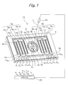
Fig. 1 is a front-side perspective view illustrating an embodiment of the optical deflector according to the presently disclosed subject matter; -
Figs. 2A and 2B are views for explaining the operation of the outer piezoelectric actuators ofFig. 1 ; -
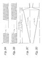
Figs. 3A, 3B, 3C and 3D are timing diagrams of the drive voltages applied to the piezoelectric actuators ofFig. 1 ; -
Fig. 4 is a cross-sectional view of the optical deflector ofFig. 1 ; -
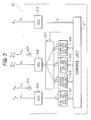
Fig. 5 is a block circuit diagram of the driver ofFig. 1 ; -
Fig. 6 is a flowchart for explaining the operation of the control unit ofFig. 5 ; -
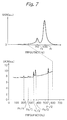
Fig. 7 is a frequency spectrum of the sense voltage ofFig. 5 , when a search sinusoidal-wave voltage is applied to the piezoelectric actuators ofFig. 1 ; -
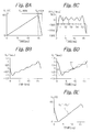
Fig. 8A is a timing diagram of the saw-tooth voltage generated by the saw-tooth voltage generating unit ofFig. 5 ; -
Fig. 8B is a timing diagram of a low-pass-filtered saw-tooth voltage generated by the flowchart ofFig. 6 ; -
Fig. 8C is a timing diagram of the differential voltage generated by the flowchart ofFig. 6 ; -
Fig. 8D is a timing diagram of the delayed low-pass-filtered saw-tooth voltage generated by the flowchart ofFig. 6 ; -
Fig. 8E is a timing diagram of the combined saw-tooth voltage generated by the flowchart ofFig. 6 ; -
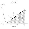
Fig. 9 is an enlargement of the timing diagram ofFig. 8E ; -
Fig. 10 is a timing diagram of the sense voltage when the combined saw-tooth voltage ofFig. 8E is applied to the piezoelectric actuators ofFig. 1 ; -
Fig. 11 is a frequency spectrum diagram of the saw-tooth voltage ofFig. 8A and the combined saw-tooth voltage ofFig. 8E ; -
Fig. 12A is a photograph showing an image obtained by driving the outer piezoelectric actuators ofFig. 1 using the low-pass-filtered saw-tooth voltages ofFig. 8A ; -
Fig. 12B is a photograph showing an image obtained by driving the outer piezoelectric actuators ofFig. 1 using the combined saw-tooth voltages ofFig. 8E ; -
Figs. 13A, 13B and 13C are diagrams for explaining the ringing phenomena of the light spots on an image frame scanned with the light of the optical deflector ofFig. 1 ; and -
Fig. 14 is a front-side perspective view illustrating a modification of the optical deflector ofFig. 1 . - In
Fig. 1 , which illustrates an embodiment of the optical deflector according to the presently disclosed subject matter as a two-dimensional MEMS device,reference numeral 10 designates a two-dimensional optical deflector, 20 designates a driver for driving theoptical deflector - The
optical deflector 10 is constructed by acircular mirror 1 for reflecting incident light L from thelaser light source 30, a pair oftorsion bars mirror 1 along an X-axis, an inner frame (movable frame) 3 surrounding themirror 1 and thetorsion bars mirror 1, a semi-ring shaped innerpiezoelectric actuator 4a coupled between thetorsion bars inner coupling portion 3a of theinner frame 3, and a semi-ring shaped innerpiezoelectric actuator 4b coupled between thetorsion bars inner coupling portion 3b of theinner frame 3. In this case, theinner frame 3 has a circular inner circumference along the innerpiezoelectric actuators piezoelectric actuator 4a is opposite to that of the innerpiezoelectric actuator 4b, so that the innerpiezoelectric actuators mirror 1 around the X-axis. - Also, the
optical deflector 10 includes an outer frame (fixed frame) 5 and a pair of meander-type outerpiezoelectric actuators coupling portions outer frame 5 andouter coupling portions inner frame 3 and serving as cantilevers for rocking themirror 1 around a Y-axis on the plane of themirror 1 centered at thecenter 0 of themirror 1. The outerpiezoelectric actuators mirror 1. - The
mirror 1 can be square, rectangular, polygonal or elliptical. In this case, the inner-circumference of theinner frame 3 is adapted to the shape of themirror 1. - In more detail, the
torsion bars mirror 1 and other ends coupled to the inner circumference of theinner frame 3. Therefore, thetorsion bars piezoelectric actuators mirror 1 around the X-axis. - The
outer frame 5 is rectangular-framed to surround theinner frame 3 associated with the meander-type outerpiezoelectric actuators - The meander-type outer
piezoelectric actuator 6a is constructed bypiezoelectric cantilevers 6a-1, 6a-2, 6a-3 and 6a-4 which are serially-coupled from thecoupling portion 5a of theouter frame 5 to thecoupling portion 3c of theinner frame 3 via folded portions Fa12, Fa23 and Fa34. Also, each of thepiezoelectric cantilevers 6a-1, 6a-2, 6a-3 and 6a-4 is in parallel with the X-axis. Therefore, thepiezoelectric cantilevers 6a-1, 6a-2, 6a-3 and 6a-4 are folded at their ends or meandering from theouter frame 5 to theinner frame 3, so that the amplitudes of thepiezoelectric cantilevers 6a-1, 6a-2, 6a-3 and 6a-4 can be changed along directions perpendicular to the Y-axis. - A
piezoelectric sensor 6a-5 is incorporated into the outermostpiezoelectric cantilever 6a-1 of the meander-type outerpiezoelectric actuator 6a to detect a sense deflection angle of themirror 1 along the Y-direction. - Similarly, the meander-type outer
piezoelectric actuator 6b is constructed bypiezoelectric cantilevers 6b-1, 6b-2, 6b-3 and 6b-4 which are serially-coupled from thecoupling portion 5b of theouter frame 5 to theouter coupling portion 3d of theinner frame 3 via folded portions Fb12, Fb23 and Fb34. Also, each of thepiezoelectric cantilevers 6b-1, 6b-2, 6b-3 and 6b-4 are in parallel with the X-axis. Therefore, thepiezoelectric cantilevers 6b-1, 6b-2, 6b-3 and 6b-4 are folded at their ends or meandering from theouter frame 5 to theinner frame 3, so that thepiezoelectric cantilevers 6b-1, 6b-2, 6b-3 and 6b-4 can be changed along directions perpendicular to the Y-axis. - The meander-type outer
piezoelectric actuators 6a (6b) operate as follows. - In the outer
piezoelectric actuators 6a (6b), thepiezoelectric cantilevers 6a-1, 6a-2, 6a-3 and 6a-4 (6b-1, 6b-2, 6b-3 and 6b-4) are divided into an odd-numbered group of thepiezoelectric cantilevers 6a-1 and 6a-3 (6b-1 and 6b-3), and an even-numbered group of thepiezoelectric cantilevers 6a-2 and 6a-4 (6b-2 and 6b-4) alternating with the odd-numbered group of thepiezoelectric cantilevers 6a-1 and 6a-3 (6b-1 and 6b-3). - When no drive voltages are applied to the
piezoelectric cantilevers 6a-1, 6a-2, 6a-3 and 6a-4, thepiezoelectric cantilevers 6a-1, 6a-2, 6a-3 and 6a-4 as well as thepiezoelectric sensor 6a-s are illustrated inFig. 2A . - On the other hand, a first drive voltage is applied to the odd-numbered group of the
piezoelectric cantilevers 6a-1 and 6a-3 and a second drive voltage opposite in phase to the first drive voltage is applied to the even-numbered group of thepiezoelectric cantilevers 6a-2 and 6a-4. For example, the odd-numbered group of thepiezoelectric cantilevers 6a-1 and 6a-3 are flexed in one direction, for example, in an upward direction U, and the even-numbered group of thepiezoelectric cantilevers 6a-2 and 6a-4 are flexed in the other direction, i. e. , in a downward direction D. Otherwise, the odd-numbered group of thepiezoelectric cantilevers 6a-1 and 6a-3 are flexed in the downward direction D, the even-numbered group of thepiezoelectric cantilevers 6a-2 and 6a-4 are flexed in the upward direction U. In this case, if the length of each of thepiezoelectric cantilevers 6a-1 and 6a-4 is about half of that of each of thepiezoelectric cantilevers 6a-2 and 6a-3, the flexing amounts of thepiezoelectric cantilevers 6a-1 and 6a-4 are about half of those of thepiezoelectric cantilevers 6a-2 and 6a-3. - Thus, the
mirror 1 is rocked around the Y-axis. - The flexing amount of the
piezoelectric actuator 6a is sensed by thepiezoelectric sensor 6a-s incorporated into thepiezoelectric actuator 6a. - Note that the number of piezoelectric cantilevers in each of the outer
piezoelectric actuators - Provided on the
outer frame 5 are pads Ps, PGa, PXa, PY1a, PY2a, PGb, PXb, PY1b and PY2b which are connected to thedriver 20. Thedriver 20 applies a drive voltage VX1 as illustrated inFig. 3A to the pad PXa and applies a drive voltage VX2 as illustrated inFig. 3B to the pad PXb. The drive voltages VX1 and VX2 are sinusoidal, and the drive voltage VX1 is opposite in phase to the drive voltage VX2. For example, the frequency fX of the drive voltages VX1 and VX2 is one resonant frequency frX such as 20 kHz depending upon a resonant structure formed by themirror 1, thetorsion bars piezoelectric actuators driver 20 applies a drive voltage VY1 as illustrated inFig. 3C to the pads PY1a and PY1b, and applies a drive voltage VY2 as illustrated inFig. 3D to the pads PY2a and PY2b. The drive voltages VY1 and VY2 are a combined (synthesized) saw-tooth voltage VYC and its inverted voltage VYC with no substantial fluctuations, and the drive voltage VY1 is opposite in phase to the drive voltage VY2. For example, the frequency fY of the drive voltages VY1 and VY2 is 60Hz, much lower than the resonant frequency frX. The combined (synthesized) saw-tooth voltage VYC will be explained later in detail. - The pad PGa, which is grounded, is connected via a via-structure (not shown) to the lower electrode layers 406 (see:
Fig. 4 ) of the innerpiezoelectric actuator 4a and thepiezoelectric cantilevers 6a-1, 6a-2, 6a-3 and 6a-4 of the outerpiezoelectric actuator 6a. - The pad PXa is connected via a wiring layer (not shown) to the upper electrode layers 408 (see:
Fig. 4 ) of the innerpiezoelectric actuator 4a. - The pad PY1a is connected via a wiring layer (not shown) to the upper electrode layers 408 (see:
Fig. 4 ) of the odd-numberedpiezoelectric cantilevers 6a-1 and 6a-3 of the outerpiezoelectric actuator 6a. - The pad PY2a is connected via a wiring layer (not shown) to the upper electrode layers 408 (see:
Fig. 4 ) of the even-numberedpiezoelectric cantilevers 6a-2 and 6a-4 of the outerpiezoelectric actuator 6a. - The pad PGb, which is grounded, is connected via a via-structure (not shown) to the lower electrode layers 406 (see:
Fig. 4 ) of the innerpiezoelectric actuator 4b and thepiezoelectric cantilevers 6b-1, 6b-2, 6b-3 and 6b-4 of the outerpiezoelectric actuator 6b. - The pad PXb is connected via a wiring layer (not shown) to the upper electrode layers 408 (see:
Fig. 4 ) of the innerpiezoelectric actuator 4b. - The pad PY1b is connected via a wiring layer (not shown) to the upper electrode layers 408 (see:
Fig. 4 ) of the odd-numberedpiezoelectric cantilevers 6b-1 and 6b-3 of the outerpiezoelectric actuator 6b. - The pad PY2b is connected via a wiring layer (not shown) to the upper electrode layers 408 (see:
Fig. 4 ) of the even-numberedpiezoelectric cantilevers 6b-2 and 6b-4 of the outerpiezoelectric actuator 6b. - The pad Ps is connected via a wiring layer (not shown) to the upper electrode layers 408 (see:
Fig. 4 ) of thepiezoelectric sensor 6a-s. - A method for manufacturing the optical deflector of
Fig. 4 is explained below. - First, a silicon-on-insulator (SOI) structure constructed by a monocrystalline silicon support layer ("Handle" layer) 401, an intermediate (buried) silicon dioxide layer ("Box" layer) 402, and a monocrystalline silicon active layer ("Device" layer) 403 is prepared. Also, by a thermal oxidation process, a
silicon dioxide layer 404 is formed on thesupport layer 401, and asilicon dioxide layer 405 is formed on theactive layer 403. Further,piezoelectric actuator cantilevers piezoelectric sensor 6a-s are formed on theactive layer 403. - Next, a Pt/Ti
lower electrode layer 406 consisting of an about 50 nm thick Ti and an about 150 nm thick Pt on Ti is formed by a sputtering process. Then, an about 3µmthick PZT layer 407 is deposited on thelower electrode layer 406 by an arc discharge reactive ion plating (ADRIP) process at a temperature of about 500°C to 600°C. Then, an about 150 nm thick Tiupper electrode layer 408 is formed on thePZT layer 407 by a sputtering process. - Next, the
upper electrode layer 408 and thePZT layer 407 are patterned by a photolithography and etching process. In this case, theupper electrode layer 408 of thepiezoelectric sensor 6a-s is electrically isolated from theupper electrode layer 408 of thepiezoelectric cantilever 6a-1. Otherwise, theupper electrode layer 408 and thePZT layer 407 of thepiezoelectric sensor 6a-s are electrically isolated from theupper electrode layer 408 and thePZT layer 407 of thepiezoelectric cantilever 6a-1. Then, thelower electrode layer 406 and thesilicon dioxide layer 405 are patterned by a photolithography and etching process. - Next, an about 500 nm thick
silicon dioxide interlayer 409 is formed on the entire surface by a plasma chemical vapor deposition (CVD) process. - Next, contact holes are perforated in the
silicon dioxide interlayer 409 by a photolithography and dry etching process. The contact holes correspond to thepiezoelectric sensor 6a-s, thepiezoelectric actuators piezoelectric cantilevers 6a-1, 6a-2, 6a-3, 6a-4, 6b-1, 6b-2, 6b-3, 6b-4, the pads Ps, PXa, PY1a, PY2a, PGa, PXb, PY1b, PY2b and PGb. - Next, wiring layers 410 made of AlCu (1%Cu) are formed by a photolithography process, a sputtering process, and a lift-off process. The wiring layers 410 are electrically connected between the upper electrode layers 408 of the
piezoelectric actuators piezoelectric sensor 6a-s, and thepiezoelectric cantilevers 6a-1, 6a-2, 6a-3, 6a-4, 6b-1, 6b-2, 6b-3 and 6b-4 and their corresponding pads Ps, PXa, PY1a, PY2a, PGa, PXb, PY1b, PY2b and PGb. - Next, the
silicon dioxide layer 404 is etched by a photolithography and dry etching process, so that thesilicon dioxide layer 404 is left in an area corresponding to theinner frame 3 and theouter frame 5. - Next, the
support layer 401 is etched by a dry etching process using thesilicon dioxide layer 404 as an etching mask. Then, thesilicon dioxide layer 402 is etched by a wet etching process using thesupport layer 401 as an etching mask. - Finally, an aluminum (Al)
reflective metal layer 411 is formed by an evaporation process on theactive layer 403, and is patterned by a photolithography and etching process, thus completing the optical deflector. - In
Fig. 4 , thetorsion bars active layer 403. - In
Fig. 5 , which is a detailed block circuit diagram of thedriver 20 ofFig. 1 , thedriver 20 is constructed by a sinusoidal-wavevoltage generating unit 201 for generating a digital sinusoidal-wave drive voltage VX1 having a resonant frequency of 20 kHz and a peak-to-peak voltage of 60V, a digital-to-analog converter 202 for converting the digital sinusoidal-wave drive voltage VX1 into an analog sinusoidal-wave drive voltage VX1 for the pad Pxa, and aninverter 203 for generating its inverted analog sinusoidal-wave drive voltage VX2 for the pad Pxb. The sinusoidal-wave generating unit 201 includes a memory such as a nonvolatile memory for storing the digital sinusoidal-wave drive voltage VX1. Note that the denotations of the analog drive voltages are the same as those of their corresponding digital drive voltages in order to simplify the description. - Also, the
driver 20 is constructed by a search sinusoidal-wavevoltage generating unit 204 for generating a digital search sinusoidal-wave voltage VYS having a frequency between 1Hz and 2kHz and a peak-to-peak voltage of 2V, a saw-tooth generating unit 205 for generating a digital saw-tooth voltage VYT having a non-resonant frequency of 60Hz and a peak-to-peak voltage of 60V, and a combined saw-toothvoltage generating unit 206 for generating a digital combined saw-tooth voltage VYC. Each of the generatingunits selector 207 and is converted by a digital-to-analog converter 208 into an analog drive voltage VY1 for the pads PY1a and PY1b. Also, aninverter 209 generates an inverted drive voltage VY2 of the drive voltage VY1 for the pads PY2a and PY2b. - Further, the
drive 20 is constructed by an analog-todigital converter 210 for converting an analog sense voltage Vs sensed by thepiezoelectric sensor 6a-s into a digital sense voltage Vs. Note that the denotation of the digital sense voltage is the same as that of the analog sense voltage, in order to simplify the description. - The sinusoidal-wave
voltage generating unit 201, the search sinusoidal-wavevoltage generating unit 204, the saw-toothvoltage generating unit 205, the combined saw-toothvoltage generating unit 206 and theselector 207 are controlled by acontrol unit 211 which receives the digital sense voltage VS from the analog-to-digital converter 210. - In
Fig. 5 , if only one of the search sinusoidal-wave generating unit 204, the saw-toothvoltage generating unit 205 and the combined saw-toothvoltage generating unit 206 is selectively operated, theselector 207 would be unnecessary. - The
control unit 211 is constructed by a digital signal processor (DSP), a field programmable gate array (FPGA) or the like. - The operation of the
control unit 211 regarding the drive voltages VY1 and VY2 and the sense voltage VS will be explained with reference to a flowchart as illustrated inFig. 6 . Note that the operation of thecontrol unit 211 regarding the drive voltages VX1 and VX2 is omitted, since the presently disclosed subject matter does not relate to the drive voltages VX1 and VX2, - The operation illustrated by the flowchart of
Fig. 6 is started by turning on the optical deflector ofFig. 1 . - First, referring to step 601, the
control unit 211 operates the search sinusoidal-wavevoltage generating unit 204 along with theselector 207. Therefore, the search sinusoidal-wavevoltage generating unit 204 generates a digital search sinusoidal-wave voltage VYS and transmits it to the digital-to-analog converter 208. In this case,

- Therefore, the
piezoelectric actuators mirror 1 around the Y-axis. In this case, the search sinusoidal-wave voltage VYS has a peak-to-peak voltage of 2V, much lower than 60V, thus preventing the optical deflector from being damaged by the resonance with the main natural frequency Fr and the pumping natural frequency Fp. The search sinusoidal-wave voltage VYS is swept from 1 Hz to 2 kHz or vice versa, preferably, from 60 Hz to 1100Hz or vice versa, for example. As a result, a frequency spectrum of the sense voltage VS from thepiezoelectric sensor 6a-s is obtained as illustrated inFig. 7 . - Next referring to step 602, a cut-off frequency fCUT-OFF is determined in accordance with the frequency spectrum of
Fig. 7 obtained bystep 601. InFig. 7 , since the main natural frequency Fr (= 1080 Hz) and the pumping natural frequency Fp (= 790 Hz) would greatly vibrate themirror 1 to damage the optical deflector, the frequencies Fr and Fp are harmful and therefore, will be removed by a low-pass filtering process which will be explained with reference tosteps - Next, referring to step 603, the
control unit 211 stops the operation of the search sinusoidal-wavevoltage generating unit 204 and operates the saw-toothvoltage generating unit 205 along with theselector 207. Therefore, the saw-toothvoltage generating unit 205 generates a digital saw-tooth voltage VYT and transmits it to the digital-to-analog converter 208. In this case,

- Therefore, the
piezoelectric actuators mirror 1 around the Y-axis. In this case, as illustrated inFig. 8A the saw-tooth voltage VYT has a peak-to-peak voltage of 60V with a frequency of 60Hz. InFig. 8A , a ratio of Ta/Tb is 9/1 where Ta is called an image active period and Tb is called a blanking period. - Next, referring to
steps piezoelectric sensor 6a-s. Concretely, atstep 604, a Fourier transform is performed upon the sense voltage VS of thepiezoelectric sensor 6a-s to obtain a Fourier frequency spectrum. Then, atstep 605, harmonic frequency components higher than the cut-off frequency fCUT-OFF are removed from the Fourier frequency spectrum to obtain a modified Fourier frequency spectrum. Then, atstep 606, an inverse-Fourier transform is performed upon the modified Fourier frequency spectrum to obtain a low-pass-filtered saw-tooth voltage VYT' as illustrated inFig. 8B . - Next, referring to step 607, the
control unit 211 differentiates the low-pass-filtered saw-tooth voltage VYT' as illustrated inFig. 8B to obtain a differential voltage Δ VYT' as illustrated inFig. 8C . Then, thecontrol unit 211 calculates a half period HP of fluctuations of the differential voltage ΔVYT' ofFig. 8C . InFig. 8C , when the differential voltage Δ VYT' is larger than a predetermined level "0", five fluctuations whose periods are defined by T1, T2, T3, T4 and T5 occur. Then, an average half period HP is calculated by
- Next, referring to step 608, the
control unit 211 delays the low-pass-filtered saw-tooth voltage VYT' ofFig. 8B by the half period HP to obtain a delayed low-pass-filtered saw-tooth voltage VYT" as illustrated inFig. 8D . Then, thecontrol unit 211 combines (synthesizes) the low-pass-filtered saw-tooth voltage VYT' ofFig. 8B with the delayed low-pass-filtered saw-tooth voltage VYT" to obtain a combined (synthesized) saw-tooth voltage VYC as illustrated inFig. 8E by
where k is a positive constant not larger than 1 (0<k ≦ 1). - In the combined saw-tooth voltage VYC as illustrated in
Fig. 8E , the fluctuation of the low-pass-filtered saw-tooth voltage VYT' as illustrated inFig. 8B is compensated for by the fluctuation of the delayed low-pass-filtered saw-tooth voltage VYT" as illustrated inFig. 8D . This is a so-called input shaping process. - Next, referring to step 609, it is determined whether or not the linearity characteristic of the combined saw-tooth voltage VYC satisfies a first predetermined condition. Ideally, the combined saw-tooth voltage VYC should have a complete linear characteristic as indicated by a straight line SL in
Fig. 9 ; however, actually the combined saw-tooth voltage VYC still has fluctuations as indicated by shaded areas F inFig. 9 . Therefore, thecontrol unit 211 calculates the shaded areas F of the combined saw-tooth voltage VYC deviated from the straight line SL inFig. 9 , and determines whether or not a ratio of the shaded areas F to a double-hatched triangular saw-tooth area below the straight line SL is smaller than a predetermined value such as 2.5%. If the ratio of the shaded areas F to the double-hatched triangular saw-tooth area is not smaller than the predetermined value, thecontrol unit 211 determines that there are still fluctuations to be compensated for in the combined saw-tooth voltage VYC, the control proceeds to step 610 which decreases the cut-off frequency fCUT-OFF by a definite value such as 50 Hz, i.e.,
- Then, the control returns to step 603 to repeat the above-mentioned processes at
step 603 to 608, thus renewing the combined saw-tooth voltage VYC. - On the other hand, if the ratio of the shaded areas to the double-hatch triangular saw-tooth area is smaller than the predetermined value, the
control unit 211 determines that there are no substantial fluctuations to be compensated for in the combined saw-tooth voltage VYC, so that the control proceeds to step 611. - Referring to step 611, the
control unit 211 stops the operation of the saw-toothvoltage generating unit 205 and operates the combined saw-tooth voltage generating 206 along with theselector 207. Therefore, the combined saw-toothvoltage generating unit 205 generates a digital combined saw-tooth voltage VYC and transmits it to the digital-to-analog converter 208. In this case,

- Therefore, the
piezoelectric actuators mirror 1 around the Y-axis. In this case, as illustrated inFig. 10 similar toFig. 9 , the sensor voltage VS has a voltage similar to the combined saw-tooth voltage VYC with a frequency of 60Hz. - Next, referring to step 612, it is determined whether or not the linearity characteristic of the sense voltage VS satisfies a second predetermined condition. Even in this case, ideally, the sense voltage VS should have a complete linear characteristic as indicated by a straight line SL' in
Fig. 10 ; however, actually the sense voltage VS still has fluctuations as indicated by shaded areas F' inFig. 10 . Therefore, thecontrol unit 211 calculates the shaded areas F' of the sense voltage VS deviated from the straight line SL' inFig. 10 , and determines whether or not a ratio of the shaded areas F' to a double-hatched triangular saw-tooth area below the straight line SL' is smaller than a predetermined value such as 2.5%. If the ratio of the shaded areas F' to the double-hatched triangular saw-tooth area is not smaller than the predetermined value, thecontrol unit 211 determines that there are still fluctuations to be compensated for in the sense voltage VS, so that the control returns to step 604 to repeat the above-mentioned processes atstep 604 to 611, thus renewing the combined saw-tooth voltage VYC. - On the other hand, if the ratio of the shaded areas F' to the double-hatched triangular saw-tooth area is smaller than the predetermined value, the
control unit 211 determines that there are no substantial fluctuations to be compensated for in the sense voltage VS, so that the control proceeds to step 613. Thus, the application of the current combined saw-tooth voltage VYC is maintained. - According to the operation according to the flowchart of
Fig. 6 , as illustrated inFig. 11 , the gain of the low-pass-filtered saw-tooth voltage VYT' where frequency components larger than 600 Hz are removed from the saw-tooth voltage VCT is decreased in a frequency region whose frequency is larger than 600Hz. Contrary to this, the gain of the combined saw-tooth voltage VYC is increased 102 times that of the low-pass-filtered saw-tooth voltage VYT'. That is, the combined saw-tooth voltage VYC rather than the low-pass-filtered saw-tooth voltage VYT' is brought close to the saw-tooth voltage VYT by the above-mentioned increase of the gain. - When the inner
piezoelectric actuators Figs. 3A and 3B and the outerpiezoelectric actuators Fig. 8B and its inverted voltage, to reflect white light L from thelight source 30, an image as illustrated inFig. 12A was obtained to exhibit traverse stripes due to the fluctuations in the low-pass-filtered saw-tooth voltage VYT'. Contrary to this, when the innerpiezoelectric actuators Figs. 3A and 3B and the outerpiezoelectric actuators Fig. 8E and its inverted voltage, to reflect white light L from thelight source 30, an image as illustrated inFig. 12B was obtained to exhibit no traverse stripes due to no substantial fluctuations in the combined saw-tooth voltage VYC. -
Figs. 13A, 13B and 13C are diagrams for showing ringing phenomena of light spots on an image frame scanned with the light L of the optical deflector ofFig. 1 which is lit at a definite time period. - As illustrated in
Fig. 13A , when the innerpiezoelectric actuators piezoelectric actuators Fig. 8B and its inverted voltage /VYT', the light spots are non-uniform in the vertical direction, so that the ringing phenomenon of the light spots in the vertical direction is large. - Also, as illustrated in
Fig. 13B , when the innerpiezoelectric actuators piezoelectric actuators - Further, as illustrated in
Fig. 13C , when the inner piezoelectric actuators are driven by the resonant sinusoidal-wave voltages VX1 and VX2 while the outerpiezoelectric actuators - In the above-described embodiment, the
piezoelectric sensor 6a-s is incorporated into thepiezoelectric cantilever 6a-1 of thepiezoelectric actuator 6a; however, thepiezoelectric sensor 6a-s can be provided at another portion of the optical deflector such as theouter frame 5. - Also, in the above-described embodiment, the
piezoelectric actuators piezoelectric actuators - Further, the presently disclosed subject matter can be applied to a one-dimensional optical deflector as illustrated in
Fig. 14 . - It will be apparent to those skilled in the art that various modifications and variations can be made in the presently disclosed subject matter without departing from the spirit or scope of the presently disclosed subject matter. Thus, it is intended that the presently disclosed subject matter covers the modifications and variations of the presently disclosed subject matter provided they come within the scope of the appended claims and their equivalents. All related or prior art references described above and in the Background section of the present specification are hereby incorporated in their entirety by reference.
Claims (12)
- A driver for driving an optical deflector including a mirror (1), a piezoelectric actuator (6a, 6b) adapted to rock said mirror (1) around a first axis of said optical deflector and a piezoelectric sensor (6a-s) adapted to sense vibrations of said piezoelectric actuator (6a, 6b),
a saw-tooth voltage generating unit (205) adapted to generate a saw-tooth voltage (VYT);
a combined saw-tooth voltage generating unit (206) adapted to generate a combined saw-tooth voltage (VYC); and
a control unit (211) adapted to control said saw-tooth voltage generating unit (205) and said combined saw-tooth voltage generating unit (206) to receive a sense voltage (Vs) from said piezoelectric sensor (6a-s),
wherein said control unit (211) operates said saw-tooth voltage generating unit (205) to apply said saw-tooth voltage (VYT) and its inverted voltage to said piezoelectric actuator (6a, 6b) to receive said sense voltage (Vs) from said piezoelectric sensor (6a-s);
performs a low-pass filtering process using a cut-off frequency (fCUT-OFF) upon said sense voltage (Vs) to obtain a low-pass-filtered saw-tooth voltage (VYT');
calculates a half period (HP) of fluctuations (F) included in said low-pass-filtered saw-tooth voltage (VYT');
combines said low-pass-filtered saw-tooth voltage (VYT') with a delayed low-pass-filtered saw-tooth voltage (VYT") obtained by delaying said low-pass-filtered saw-tooth voltage (VYT') by said half period (HP), to obtain a combined saw-tooth voltage (VYC); and
operates said combined saw-tooth voltage generating unit (206) to apply said combined saw-tooth voltage (VYC) and its inverted voltage to said piezoelectric actuator (6a, 6b). - The driver as set forth in claim 1, wherein said control unit (211) calculates a first linearity characteristic of said sense voltage (Vs) while applying said saw-tooth voltage (VYT) and its inverted voltage to said piezoelectric actuator (6a, 6b);
determines whether or not said first linearity characteristic of said sense voltage (Vs) satisfies a first predetermined condition; and
continues application of said saw-tooth voltage (VYT) and its inverted voltage to said piezoelectric actuator (6a, 6b) to renew said combined saw-tooth voltage (VYC) by decreasing said cut-off frequency (fCUT-OFF) by a predetermined amount, until said first linearity characteristic of said sense voltage (Vs) satisfies said first predetermined condition. - The driver as set forth in claim 2, wherein said control unit (211) calculates a second linearity characteristic of said sense voltage (Vs) while applying said combined saw-tooth voltage (VYC) and its inverted voltage to said piezoelectric actuator (6a, 6b);
determines whether or not said second linearity characteristic of said sense voltage (Vs) satisfies a second predetermined condition; and
renews said combined saw-tooth voltage (VYC) until said second linearity characteristic of said sense voltage (Vs) satisfies said second predetermined condition. - The driver as set forth in claim 1, further comprising a search sinusoidal-wave voltage generating unit (204) adapted to a search sinusoidal-wave voltage (VYS),
wherein said control unit (211) operates said search sinusoidal-wave voltage generating unit (204) to apply said search sinusoidal-wave voltage (VYS) and its inverted voltage to said piezoelectric actuator (6a, 6b) while sweeping the frequency of said search sinusoidal-wave voltage (VYS) to receive said sense voltage (Vs) from said piezoelectric sensor (6a-s); and
initially determines a cut-off frequency (fCUT-OFF) of said low-pass-filtered process in accordance with said sense voltage (Vs) from said piezoelectric sensor (6a-s) while applying said search sinusoidal-wave voltage (VYS) and its inverted voltage to said piezoelectric actuator (6a, 6b). - The driver as set forth in claim 1, wherein said piezoelectric actuator (6a, 6b) comprises a first group of piezoelectric cantilevers (6a-1, 6a-3; 6b-1, 6b-3) and a second group of piezoelectric cantilevers (6a-2, 6a-4; 6b-2, 6b-4) alternating with said first group of piezoelectric cantilevers (6a-1, 6a-3; 6b-1, 6b-3) folded at their ends and in parallel with a second axis perpendicular to said first axis,
wherein a voltage applied to said first group of piezoelectric cantilevers (6a-1, 6a-3; 6b-1, 6b-3) is opposite in phase to a voltage supplied to said second group of piezoelectric cantilevers (6a-2, 6a-4; 6b-2, 6b-4). - The driver as set forth in claim 5, wherein said piezoelectric sensor (6a-s) is incorporated into one of said piezoelectric cantilevers (6a-1).
- A method for controlling an optical deflector including a mirror (1), a piezoelectric actuator (6a, 6b) adapted to rock said mirror (1) around a first axis of said optical deflector and a piezoelectric sensor (6a-s) adapted to sense vibrations of said piezoelectric actuator (6a, 6b),
said method comprising:applying a saw-tooth voltage (VYT) and its inverted voltage to said piezoelectric actuator (6a, 6b) to receive said sense voltage (Vs) from said piezoelectric sensor (6a-s) ;performing a low-pass filtering process using a cut-off frequency (fCUT-OFF) upon said sense voltage (Vs) to obtain a low-pass-filtered saw-tooth voltage (VYT');calculating a half period (HP) of fluctuations (F) included in said low-pass-filtered saw-tooth voltage (VYT');combining said low-pass-filtered saw-tooth voltage (VYT') with a delayed low-pass-filtered saw-tooth voltage (VYT") obtained by delaying said low-pass-filtered saw-tooth voltage (VYT') by said half period (HP), to obtain a combined saw-tooth voltage (VYC) ; andapplying said combined saw-tooth voltage (VYC) and its inverted voltage to said piezoelectric actuator (6a, 6b). - The method as set forth in claim 7, further comprising:calculating a first linearity characteristic of said sense voltage (Vs) while applying said saw-tooth voltage (VYT) and its inverted voltage to said piezoelectric actuator (6a, 6b);determining whether or not said first linearity characteristic of said sense voltage (Vs) satisfies a first predetermined condition; andcontinuing application of said saw-tooth voltage (VYT) and its inverted voltage to said piezoelectric actuator (6a, 6b) to renew said combined saw-tooth voltage (VYC) by decreasing said cut-off frequency (fCUT-OFF) by a predetermined amount, until said first linearity characteristic of said sense voltage (Vs) satisfies said first predetermined condition.
- The driver as set forth in claim 8, further comprising:calculating a second linearity characteristic of said sense voltage (Vs) while applying said combined saw-tooth voltage (VYC) and its inverted voltage to said piezoelectric actuator (6a, 6b);determining whether or not said second linearity characteristic of said sense voltage (Vs) satisfies a second predetermined condition; andrenewing said combined saw-tooth voltage (VYC) until said second linearity characteristic of said sense voltage (Vs) satisfies said second predetermined condition.
- The method as set forth in claim 7, further comprising:applying a search sinusoidal-wave voltage (VYS) and its inverted voltage to said piezoelectric actuator (6a, 6b) while sweeping the frequency of said search sinusoidal-wave voltage (VYS) to receive said sense voltage (Vs) from said piezoelectric sensor (6a-s) andinitially determining a cut-off frequency (fCUT-OFF) of said low-pass-filtered process in accordance with said sense voltage (Vs) from said piezoelectric sensor (6a-s) while applying said search sinusoidal-wave voltage (VYS) and its inverted voltage to said piezoelectric actuator (6a, 6b).
- The method as set forth in claim 7, wherein said piezoelectric actuator (6a, 6b) comprises a first group of piezoelectric cantilevers (6a-1, 6a-3; 6b-1, 6b-3) and a second group of piezoelectric cantilevers (6a-2, 6a-4; 6b-2, 6b-4) alternating with said first group of piezoelectric cantilevers (6a-1, 6a-3; 6b-1, 6b-3) folded at their ends and in parallel with a second axis perpendicular to said first axis,
wherein a voltage applied to said first group of piezoelectric cantilevers (6a-1, 6a-3; 6b-1, 6b-3) is opposite in phase to a voltage supplied to said second group of piezoelectric cantilevers (6a-2, 6a-4; 6b-2, 6b-4). - The method as set forth in claim 11, wherein said piezoelectric sensor (6a-s) is incorporated into one of said piezoelectric cantilever 6a-1.
Applications Claiming Priority (1)
| Application Number | Priority Date | Filing Date | Title |
|---|---|---|---|
| JP2014114759A JP6324817B2 (en) | 2014-06-03 | 2014-06-03 | Optical scanner and optical deflector control method |
Publications (2)
| Publication Number | Publication Date |
|---|---|
| EP2953125A1 true EP2953125A1 (en) | 2015-12-09 |
| EP2953125B1 EP2953125B1 (en) | 2017-11-01 |
Family
ID=53385490
Family Applications (1)
| Application Number | Title | Priority Date | Filing Date |
|---|---|---|---|
| EP15170301.4A Active EP2953125B1 (en) | 2014-06-03 | 2015-06-02 | Driver for optical deflector using combined saw-tooth drive voltage and method for controlling the same |
Country Status (3)
| Country | Link |
|---|---|
| US (1) | US9893263B2 (en) |
| EP (1) | EP2953125B1 (en) |
| JP (1) | JP6324817B2 (en) |
Cited By (1)
| Publication number | Priority date | Publication date | Assignee | Title |
|---|---|---|---|---|
| CN108427190A (en) * | 2017-02-14 | 2018-08-21 | 三美电机株式会社 | Light scanning apparatus and light scan method |
Families Citing this family (13)
| Publication number | Priority date | Publication date | Assignee | Title |
|---|---|---|---|---|
| JP6493014B2 (en) * | 2015-06-25 | 2019-04-03 | 株式会社デンソー | Optical scanning device |
| CN108227181B (en) * | 2017-12-08 | 2020-06-16 | 华为技术有限公司 | A beam scanning device of an array rotating mirror |
| CN112912784B (en) * | 2018-10-25 | 2022-11-11 | 富士胶片株式会社 | Micromirror device and driving method of micromirror device |
| JP7172557B2 (en) * | 2018-12-19 | 2022-11-16 | 株式会社リコー | Optical deflection device, image projection device, laser headlamp and moving object |
| JP2020101590A (en) * | 2018-12-19 | 2020-07-02 | 株式会社リコー | Light deflection device, image projection device, and moving body |
| JP7263918B2 (en) | 2019-05-21 | 2023-04-25 | 株式会社リコー | Optical deflection device, image projection device, vehicle, and adjustment method |
| JP7315827B2 (en) * | 2019-07-01 | 2023-07-27 | ミツミ電機株式会社 | Optical scanning device and its control method |
| US11750779B2 (en) * | 2019-08-20 | 2023-09-05 | Ricoh Company, Ltd. | Light deflector, optical scanning system, image projection device, image forming apparatus, and lidar device |
| JP7316927B2 (en) * | 2019-12-05 | 2023-07-28 | 富士フイルム株式会社 | Piezoelectric MEMS device, manufacturing method and driving method |
| JP7316926B2 (en) * | 2019-12-05 | 2023-07-28 | 富士フイルム株式会社 | Piezoelectric MEMS device, manufacturing method and driving method |
| WO2021199223A1 (en) * | 2020-03-30 | 2021-10-07 | 国立大学法人東海国立大学機構 | Cutting apparatus and cutting method |
| KR102892297B1 (en) * | 2020-11-03 | 2025-11-26 | 삼성전자주식회사 | Micromechanical resonator and resonator system including the same |
| JP7593186B2 (en) * | 2021-03-18 | 2024-12-03 | 株式会社リコー | Optical deflector, image projection device, head-up display, laser headlamp, head-mounted display, distance measuring device, and moving body |
Citations (7)
| Publication number | Priority date | Publication date | Assignee | Title |
|---|---|---|---|---|
| US20080239252A1 (en) | 2007-03-29 | 2008-10-02 | Konica Minolta Opto, Inc. | Image projector |
| US20080297869A1 (en) | 2007-06-04 | 2008-12-04 | Canon Kabushiki Kaisha | Oscillator device and drive control method for oscillation system of oscillator device |
| JP2009223165A (en) | 2008-03-18 | 2009-10-01 | Stanley Electric Co Ltd | Optical deflector |
| US20110109950A1 (en) * | 2008-07-16 | 2011-05-12 | Brother Kogyo Kabushiki Kaisha | Drive signal generator and optical scanning device provided with drive signal generator, and image display device |
| US20120327494A1 (en) * | 2011-06-22 | 2012-12-27 | Takaaki Koyama | Optical deflector including piezoelectric sensor on support body |
| JP2013171226A (en) | 2012-02-22 | 2013-09-02 | Funai Electric Co Ltd | Image display device and mirror driving method of the same |
| EP2645148A1 (en) * | 2012-03-29 | 2013-10-02 | Stanley Electric Co., Ltd. | Optical deflector |
Family Cites Families (4)
| Publication number | Priority date | Publication date | Assignee | Title |
|---|---|---|---|---|
| KR100803208B1 (en) * | 2006-01-17 | 2008-02-14 | 삼성전자주식회사 | A computer readable recording medium recording an image display device and method and a program for executing the same on a computer |
| JP2012137692A (en) * | 2010-12-27 | 2012-07-19 | Brother Ind Ltd | Image display device |
| JP5890115B2 (en) * | 2011-06-22 | 2016-03-22 | スタンレー電気株式会社 | Optical deflector |
| JP2013200337A (en) * | 2012-03-23 | 2013-10-03 | Stanley Electric Co Ltd | Light deflector |
-
2014
- 2014-06-03 JP JP2014114759A patent/JP6324817B2/en active Active
-
2015
- 2015-05-28 US US14/724,344 patent/US9893263B2/en active Active
- 2015-06-02 EP EP15170301.4A patent/EP2953125B1/en active Active
Patent Citations (10)
| Publication number | Priority date | Publication date | Assignee | Title |
|---|---|---|---|---|
| US20080239252A1 (en) | 2007-03-29 | 2008-10-02 | Konica Minolta Opto, Inc. | Image projector |
| JP2008249797A (en) | 2007-03-29 | 2008-10-16 | Konica Minolta Opto Inc | Image projector |
| US20080297869A1 (en) | 2007-06-04 | 2008-12-04 | Canon Kabushiki Kaisha | Oscillator device and drive control method for oscillation system of oscillator device |
| JP2008299297A (en) | 2007-06-04 | 2008-12-11 | Canon Inc | Oscillator device and drive control method of oscillation system of oscillator device |
| JP2009223165A (en) | 2008-03-18 | 2009-10-01 | Stanley Electric Co Ltd | Optical deflector |
| US20110109950A1 (en) * | 2008-07-16 | 2011-05-12 | Brother Kogyo Kabushiki Kaisha | Drive signal generator and optical scanning device provided with drive signal generator, and image display device |
| US20120327494A1 (en) * | 2011-06-22 | 2012-12-27 | Takaaki Koyama | Optical deflector including piezoelectric sensor on support body |
| JP2013171226A (en) | 2012-02-22 | 2013-09-02 | Funai Electric Co Ltd | Image display device and mirror driving method of the same |
| US20150043047A1 (en) | 2012-02-22 | 2015-02-12 | Funai Electric Co., Ltd. | Image Display Device and Mirror Driving Method Therefor |
| EP2645148A1 (en) * | 2012-03-29 | 2013-10-02 | Stanley Electric Co., Ltd. | Optical deflector |
Non-Patent Citations (1)
| Title |
|---|
| DR CAMPBELL - UNIVERSITY OF PAISLEY: "An introduction to digital filters", 25 September 2007 (2007-09-25), XP002745082, Retrieved from the Internet <URL:http://media.paisley.ac.uk/~campbell/ASP/Lecture10/DigFiltIntro.PDF> [retrieved on 20150925] * |
Cited By (2)
| Publication number | Priority date | Publication date | Assignee | Title |
|---|---|---|---|---|
| CN108427190A (en) * | 2017-02-14 | 2018-08-21 | 三美电机株式会社 | Light scanning apparatus and light scan method |
| CN108427190B (en) * | 2017-02-14 | 2021-11-09 | 三美电机株式会社 | Optical scanning device and optical scanning method |
Also Published As
| Publication number | Publication date |
|---|---|
| EP2953125B1 (en) | 2017-11-01 |
| US9893263B2 (en) | 2018-02-13 |
| JP2015230326A (en) | 2015-12-21 |
| JP6324817B2 (en) | 2018-05-16 |
| US20150349237A1 (en) | 2015-12-03 |
Similar Documents
| Publication | Publication Date | Title |
|---|---|---|
| EP2953125B1 (en) | Driver for optical deflector using combined saw-tooth drive voltage and method for controlling the same | |
| JP6891402B2 (en) | Adjustment method of light deflector, image forming device, image display device, object device, and light deflector | |
| EP2955561B1 (en) | Optical deflector apparatus capable of increasing offset deflecting amount of mirror | |
| US9696541B2 (en) | Two-dimensional optical deflector including two SOI structures and its manufacturing method | |
| EP2503375B1 (en) | Driver for optical deflector using two modified synchronous saw-tooth drive voltages and method for setting the same | |
| JP6641709B2 (en) | Optical deflection device, image forming device, image display device, moving body device, and adjustment method for optical deflection device | |
| EP2808719B1 (en) | Optical deflector including separated piezoelectric portions on piezoelectric actuators | |
| EP2781948B1 (en) | Optical deflector including meander-type piezoelectric actuators coupled by crossing bars therebetween | |
| US11143863B2 (en) | Optical scanning device | |
| US8270057B2 (en) | Oscillator device, optical deflecting device and method of controlling the same | |
| JP2016114798A (en) | Optical deflector and manufacturing method for optical deflector | |
| US9436000B2 (en) | Optical deflector including meander-type piezoelectric actuators and ill-balanced mirror structure | |
| JP2011069954A (en) | Optical scanner | |
| US7933057B2 (en) | Oscillator device, optical deflector and image forming apparatus using the optical deflector | |
| JP7027689B2 (en) | Light deflector and image projection device | |
| US20240288683A1 (en) | Microscanner having meander spring-based mirror suspension | |
| US10908411B2 (en) | Actuator and optical scanning device | |
| JP7161094B2 (en) | SCANNING DRIVE DEVICE, OPTICAL SCANNING CONTROL DEVICE, AND DRIVING WAVEFORM GENERATION METHOD | |
| JP6990960B2 (en) | 2D optical deflector | |
| JP5299489B2 (en) | Actuator, optical scanner, and image forming apparatus | |
| JP5299482B2 (en) | Actuator, optical scanner, and image forming apparatus | |
| JP7053296B2 (en) | 2D optical deflector |
Legal Events
| Date | Code | Title | Description |
|---|---|---|---|
| PUAI | Public reference made under article 153(3) epc to a published international application that has entered the european phase |
Free format text: ORIGINAL CODE: 0009012 |
|
| AK | Designated contracting states |
Kind code of ref document: A1 Designated state(s): AL AT BE BG CH CY CZ DE DK EE ES FI FR GB GR HR HU IE IS IT LI LT LU LV MC MK MT NL NO PL PT RO RS SE SI SK SM TR |
|
| AX | Request for extension of the european patent |
Extension state: BA ME |
|
| 17P | Request for examination filed |
Effective date: 20160609 |
|
| RBV | Designated contracting states (corrected) |
Designated state(s): AL AT BE BG CH CY CZ DE DK EE ES FI FR GB GR HR HU IE IS IT LI LT LU LV MC MK MT NL NO PL PT RO RS SE SI SK SM TR |
|
| R17P | Request for examination filed (corrected) |
Effective date: 20160609 |
|
| REG | Reference to a national code |
Ref country code: DE Ref legal event code: R079 Ref document number: 602015005675 Country of ref document: DE Free format text: PREVIOUS MAIN CLASS: G09G0003340000 Ipc: H01L0041040000 |
|
| GRAP | Despatch of communication of intention to grant a patent |
Free format text: ORIGINAL CODE: EPIDOSNIGR1 |
|
| RIC1 | Information provided on ipc code assigned before grant |
Ipc: G02B 26/02 20060101ALI20170411BHEP Ipc: G09G 3/02 20060101ALI20170411BHEP Ipc: H01L 41/04 20060101AFI20170411BHEP Ipc: G02B 26/08 20060101ALI20170411BHEP Ipc: G02B 26/10 20060101ALI20170411BHEP |
|
| INTG | Intention to grant announced |
Effective date: 20170511 |
|
| RIN1 | Information on inventor provided before grant (corrected) |
Inventor name: AIMONO, TAKANORI |
|
| GRAS | Grant fee paid |
Free format text: ORIGINAL CODE: EPIDOSNIGR3 |
|
| GRAA | (expected) grant |
Free format text: ORIGINAL CODE: 0009210 |
|
| AK | Designated contracting states |
Kind code of ref document: B1 Designated state(s): AL AT BE BG CH CY CZ DE DK EE ES FI FR GB GR HR HU IE IS IT LI LT LU LV MC MK MT NL NO PL PT RO RS SE SI SK SM TR |
|
| REG | Reference to a national code |
Ref country code: GB Ref legal event code: FG4D |
|
| REG | Reference to a national code |
Ref country code: CH Ref legal event code: EP Ref country code: AT Ref legal event code: REF Ref document number: 942847 Country of ref document: AT Kind code of ref document: T Effective date: 20171115 |
|
| REG | Reference to a national code |
Ref country code: IE Ref legal event code: FG4D |
|
| REG | Reference to a national code |
Ref country code: DE Ref legal event code: R096 Ref document number: 602015005675 Country of ref document: DE |
|
| REG | Reference to a national code |
Ref country code: NL Ref legal event code: MP Effective date: 20171101 |
|
| REG | Reference to a national code |
Ref country code: LT Ref legal event code: MG4D |
|
| REG | Reference to a national code |
Ref country code: AT Ref legal event code: MK05 Ref document number: 942847 Country of ref document: AT Kind code of ref document: T Effective date: 20171101 |
|
| PG25 | Lapsed in a contracting state [announced via postgrant information from national office to epo] |
Ref country code: LT Free format text: LAPSE BECAUSE OF FAILURE TO SUBMIT A TRANSLATION OF THE DESCRIPTION OR TO PAY THE FEE WITHIN THE PRESCRIBED TIME-LIMIT Effective date: 20171101 Ref country code: NO Free format text: LAPSE BECAUSE OF FAILURE TO SUBMIT A TRANSLATION OF THE DESCRIPTION OR TO PAY THE FEE WITHIN THE PRESCRIBED TIME-LIMIT Effective date: 20180201 Ref country code: FI Free format text: LAPSE BECAUSE OF FAILURE TO SUBMIT A TRANSLATION OF THE DESCRIPTION OR TO PAY THE FEE WITHIN THE PRESCRIBED TIME-LIMIT Effective date: 20171101 Ref country code: NL Free format text: LAPSE BECAUSE OF FAILURE TO SUBMIT A TRANSLATION OF THE DESCRIPTION OR TO PAY THE FEE WITHIN THE PRESCRIBED TIME-LIMIT Effective date: 20171101 Ref country code: ES Free format text: LAPSE BECAUSE OF FAILURE TO SUBMIT A TRANSLATION OF THE DESCRIPTION OR TO PAY THE FEE WITHIN THE PRESCRIBED TIME-LIMIT Effective date: 20171101 Ref country code: SE Free format text: LAPSE BECAUSE OF FAILURE TO SUBMIT A TRANSLATION OF THE DESCRIPTION OR TO PAY THE FEE WITHIN THE PRESCRIBED TIME-LIMIT Effective date: 20171101 |
|
| REG | Reference to a national code |
Ref country code: FR Ref legal event code: PLFP Year of fee payment: 4 |
|
| PG25 | Lapsed in a contracting state [announced via postgrant information from national office to epo] |
Ref country code: RS Free format text: LAPSE BECAUSE OF FAILURE TO SUBMIT A TRANSLATION OF THE DESCRIPTION OR TO PAY THE FEE WITHIN THE PRESCRIBED TIME-LIMIT Effective date: 20171101 Ref country code: HR Free format text: LAPSE BECAUSE OF FAILURE TO SUBMIT A TRANSLATION OF THE DESCRIPTION OR TO PAY THE FEE WITHIN THE PRESCRIBED TIME-LIMIT Effective date: 20171101 Ref country code: GR Free format text: LAPSE BECAUSE OF FAILURE TO SUBMIT A TRANSLATION OF THE DESCRIPTION OR TO PAY THE FEE WITHIN THE PRESCRIBED TIME-LIMIT Effective date: 20180202 Ref country code: LV Free format text: LAPSE BECAUSE OF FAILURE TO SUBMIT A TRANSLATION OF THE DESCRIPTION OR TO PAY THE FEE WITHIN THE PRESCRIBED TIME-LIMIT Effective date: 20171101 Ref country code: AT Free format text: LAPSE BECAUSE OF FAILURE TO SUBMIT A TRANSLATION OF THE DESCRIPTION OR TO PAY THE FEE WITHIN THE PRESCRIBED TIME-LIMIT Effective date: 20171101 Ref country code: BG Free format text: LAPSE BECAUSE OF FAILURE TO SUBMIT A TRANSLATION OF THE DESCRIPTION OR TO PAY THE FEE WITHIN THE PRESCRIBED TIME-LIMIT Effective date: 20180201 Ref country code: IS Free format text: LAPSE BECAUSE OF FAILURE TO SUBMIT A TRANSLATION OF THE DESCRIPTION OR TO PAY THE FEE WITHIN THE PRESCRIBED TIME-LIMIT Effective date: 20180301 |
|
| PG25 | Lapsed in a contracting state [announced via postgrant information from national office to epo] |
Ref country code: EE Free format text: LAPSE BECAUSE OF FAILURE TO SUBMIT A TRANSLATION OF THE DESCRIPTION OR TO PAY THE FEE WITHIN THE PRESCRIBED TIME-LIMIT Effective date: 20171101 Ref country code: CY Free format text: LAPSE BECAUSE OF FAILURE TO SUBMIT A TRANSLATION OF THE DESCRIPTION OR TO PAY THE FEE WITHIN THE PRESCRIBED TIME-LIMIT Effective date: 20171101 Ref country code: DK Free format text: LAPSE BECAUSE OF FAILURE TO SUBMIT A TRANSLATION OF THE DESCRIPTION OR TO PAY THE FEE WITHIN THE PRESCRIBED TIME-LIMIT Effective date: 20171101 Ref country code: CZ Free format text: LAPSE BECAUSE OF FAILURE TO SUBMIT A TRANSLATION OF THE DESCRIPTION OR TO PAY THE FEE WITHIN THE PRESCRIBED TIME-LIMIT Effective date: 20171101 Ref country code: SK Free format text: LAPSE BECAUSE OF FAILURE TO SUBMIT A TRANSLATION OF THE DESCRIPTION OR TO PAY THE FEE WITHIN THE PRESCRIBED TIME-LIMIT Effective date: 20171101 |
|
| REG | Reference to a national code |
Ref country code: DE Ref legal event code: R097 Ref document number: 602015005675 Country of ref document: DE |
|
| PG25 | Lapsed in a contracting state [announced via postgrant information from national office to epo] |
Ref country code: SM Free format text: LAPSE BECAUSE OF FAILURE TO SUBMIT A TRANSLATION OF THE DESCRIPTION OR TO PAY THE FEE WITHIN THE PRESCRIBED TIME-LIMIT Effective date: 20171101 Ref country code: IT Free format text: LAPSE BECAUSE OF FAILURE TO SUBMIT A TRANSLATION OF THE DESCRIPTION OR TO PAY THE FEE WITHIN THE PRESCRIBED TIME-LIMIT Effective date: 20171101 Ref country code: RO Free format text: LAPSE BECAUSE OF FAILURE TO SUBMIT A TRANSLATION OF THE DESCRIPTION OR TO PAY THE FEE WITHIN THE PRESCRIBED TIME-LIMIT Effective date: 20171101 Ref country code: PL Free format text: LAPSE BECAUSE OF FAILURE TO SUBMIT A TRANSLATION OF THE DESCRIPTION OR TO PAY THE FEE WITHIN THE PRESCRIBED TIME-LIMIT Effective date: 20171101 |
|
| PLBE | No opposition filed within time limit |
Free format text: ORIGINAL CODE: 0009261 |
|
| STAA | Information on the status of an ep patent application or granted ep patent |
Free format text: STATUS: NO OPPOSITION FILED WITHIN TIME LIMIT |
|
| 26N | No opposition filed |
Effective date: 20180802 |
|
| PG25 | Lapsed in a contracting state [announced via postgrant information from national office to epo] |
Ref country code: SI Free format text: LAPSE BECAUSE OF FAILURE TO SUBMIT A TRANSLATION OF THE DESCRIPTION OR TO PAY THE FEE WITHIN THE PRESCRIBED TIME-LIMIT Effective date: 20171101 |
|
| REG | Reference to a national code |
Ref country code: CH Ref legal event code: PL |
|
| REG | Reference to a national code |
Ref country code: BE Ref legal event code: MM Effective date: 20180630 |
|
| REG | Reference to a national code |
Ref country code: IE Ref legal event code: MM4A |
|
| PG25 | Lapsed in a contracting state [announced via postgrant information from national office to epo] |
Ref country code: MC Free format text: LAPSE BECAUSE OF FAILURE TO SUBMIT A TRANSLATION OF THE DESCRIPTION OR TO PAY THE FEE WITHIN THE PRESCRIBED TIME-LIMIT Effective date: 20171101 Ref country code: LU Free format text: LAPSE BECAUSE OF NON-PAYMENT OF DUE FEES Effective date: 20180602 |
|
| PG25 | Lapsed in a contracting state [announced via postgrant information from national office to epo] |
Ref country code: LI Free format text: LAPSE BECAUSE OF NON-PAYMENT OF DUE FEES Effective date: 20180630 Ref country code: IE Free format text: LAPSE BECAUSE OF NON-PAYMENT OF DUE FEES Effective date: 20180602 Ref country code: CH Free format text: LAPSE BECAUSE OF NON-PAYMENT OF DUE FEES Effective date: 20180630 |
|
| PG25 | Lapsed in a contracting state [announced via postgrant information from national office to epo] |
Ref country code: BE Free format text: LAPSE BECAUSE OF NON-PAYMENT OF DUE FEES Effective date: 20180630 |
|
| PG25 | Lapsed in a contracting state [announced via postgrant information from national office to epo] |
Ref country code: MT Free format text: LAPSE BECAUSE OF NON-PAYMENT OF DUE FEES Effective date: 20180602 |
|
| PG25 | Lapsed in a contracting state [announced via postgrant information from national office to epo] |
Ref country code: TR Free format text: LAPSE BECAUSE OF FAILURE TO SUBMIT A TRANSLATION OF THE DESCRIPTION OR TO PAY THE FEE WITHIN THE PRESCRIBED TIME-LIMIT Effective date: 20171101 |
|
| PG25 | Lapsed in a contracting state [announced via postgrant information from national office to epo] |
Ref country code: PT Free format text: LAPSE BECAUSE OF FAILURE TO SUBMIT A TRANSLATION OF THE DESCRIPTION OR TO PAY THE FEE WITHIN THE PRESCRIBED TIME-LIMIT Effective date: 20171101 |
|
| PG25 | Lapsed in a contracting state [announced via postgrant information from national office to epo] |
Ref country code: MK Free format text: LAPSE BECAUSE OF NON-PAYMENT OF DUE FEES Effective date: 20171101 Ref country code: HU Free format text: LAPSE BECAUSE OF FAILURE TO SUBMIT A TRANSLATION OF THE DESCRIPTION OR TO PAY THE FEE WITHIN THE PRESCRIBED TIME-LIMIT; INVALID AB INITIO Effective date: 20150602 |
|
| PG25 | Lapsed in a contracting state [announced via postgrant information from national office to epo] |
Ref country code: AL Free format text: LAPSE BECAUSE OF FAILURE TO SUBMIT A TRANSLATION OF THE DESCRIPTION OR TO PAY THE FEE WITHIN THE PRESCRIBED TIME-LIMIT Effective date: 20171101 |
|
| REG | Reference to a national code |
Ref country code: DE Ref legal event code: R079 Ref document number: 602015005675 Country of ref document: DE Free format text: PREVIOUS MAIN CLASS: H01L0041040000 Ipc: H10N0030800000 |
|
| PGFP | Annual fee paid to national office [announced via postgrant information from national office to epo] |
Ref country code: GB Payment date: 20240502 Year of fee payment: 10 |
|
| PGFP | Annual fee paid to national office [announced via postgrant information from national office to epo] |
Ref country code: FR Payment date: 20240509 Year of fee payment: 10 |
|
| PGFP | Annual fee paid to national office [announced via postgrant information from national office to epo] |
Ref country code: DE Payment date: 20250429 Year of fee payment: 11 |
|
| GBPC | Gb: european patent ceased through non-payment of renewal fee |
Effective date: 20250602 |
|
| PG25 | Lapsed in a contracting state [announced via postgrant information from national office to epo] |
Ref country code: GB Free format text: LAPSE BECAUSE OF NON-PAYMENT OF DUE FEES Effective date: 20250602 |
|
| PG25 | Lapsed in a contracting state [announced via postgrant information from national office to epo] |
Ref country code: FR Free format text: LAPSE BECAUSE OF NON-PAYMENT OF DUE FEES Effective date: 20250630 |