EP2950449A1 - Attenuator - Google Patents
Attenuator Download PDFInfo
- Publication number
- EP2950449A1 EP2950449A1 EP14305800.6A EP14305800A EP2950449A1 EP 2950449 A1 EP2950449 A1 EP 2950449A1 EP 14305800 A EP14305800 A EP 14305800A EP 2950449 A1 EP2950449 A1 EP 2950449A1
- Authority
- EP
- European Patent Office
- Prior art keywords
- impedance
- attenuator
- impedance device
- network
- input signal
- Prior art date
- Legal status (The legal status is an assumption and is not a legal conclusion. Google has not performed a legal analysis and makes no representation as to the accuracy of the status listed.)
- Withdrawn
Links
- 230000002238 attenuated effect Effects 0.000 claims abstract description 13
- 238000000034 method Methods 0.000 claims abstract description 10
- 230000008878 coupling Effects 0.000 claims description 25
- 238000010168 coupling process Methods 0.000 claims description 25
- 238000005859 coupling reaction Methods 0.000 claims description 25
- 230000005669 field effect Effects 0.000 claims description 6
- 239000003990 capacitor Substances 0.000 claims description 4
- 238000003780 insertion Methods 0.000 abstract description 33
- 230000037431 insertion Effects 0.000 abstract description 33
- 230000003071 parasitic effect Effects 0.000 description 15
- 238000005516 engineering process Methods 0.000 description 7
- 230000006870 function Effects 0.000 description 6
- 230000001419 dependent effect Effects 0.000 description 5
- 238000010586 diagram Methods 0.000 description 3
- 239000004065 semiconductor Substances 0.000 description 3
- 238000010521 absorption reaction Methods 0.000 description 2
- 230000005540 biological transmission Effects 0.000 description 2
- 230000015556 catabolic process Effects 0.000 description 2
- 239000013256 coordination polymer Substances 0.000 description 2
- 238000013500 data storage Methods 0.000 description 2
- 230000015654 memory Effects 0.000 description 2
- 230000008094 contradictory effect Effects 0.000 description 1
- 230000000694 effects Effects 0.000 description 1
- 238000005538 encapsulation Methods 0.000 description 1
- 230000003993 interaction Effects 0.000 description 1
- 238000004806 packaging method and process Methods 0.000 description 1
- 230000008569 process Effects 0.000 description 1
- 230000009467 reduction Effects 0.000 description 1
- 230000010076 replication Effects 0.000 description 1
- 238000004088 simulation Methods 0.000 description 1
- 238000006467 substitution reaction Methods 0.000 description 1
- 230000007704 transition Effects 0.000 description 1
Images


Classifications
-
- H—ELECTRICITY
- H03—ELECTRONIC CIRCUITRY
- H03H—IMPEDANCE NETWORKS, e.g. RESONANT CIRCUITS; RESONATORS
- H03H7/00—Multiple-port networks comprising only passive electrical elements as network components
- H03H7/24—Frequency- independent attenuators
- H03H7/25—Frequency- independent attenuators comprising an element controlled by an electric or magnetic variable
- H03H7/253—Frequency- independent attenuators comprising an element controlled by an electric or magnetic variable the element being a diode
- H03H7/255—Frequency- independent attenuators comprising an element controlled by an electric or magnetic variable the element being a diode the element being a PIN diode
Definitions
- the present invention relates to an attenuator and a method.
- Attenuators are known.
- RF attenuators are widely used in radar systems, point to point radio, smart antennas and in radio frequency (RF) signal cancellation.
- the choice of antenna for a particular application is influenced by many factors, such as the required dynamic range, insertion losses, power consumption, linearity and power handling capabilities.
- PIN diodes or field effect transistors (FETs) are usually used to achieve such attenuation.
- FETs field effect transistors
- These devices are well suited for use as attenuators because the resistance of a PIN diode is direct current (DC) current controlled and so the higher the current through the PIN diode, the lower the resistance.
- the resistance of FET based attenuators is DC voltage controlled, typically in the order of a few volts, which depends on the breakdown voltage of the gate-source junction.
- an attenuator comprising: an input operable to receive an input signal to be attenuated; a coupling device coupled with the input and with an output providing an attenuated input signal; and a pair of reflective loads coupled with the coupling device to receive the input signal, each reflective load comprising a first impedance network arranged in parallel with a second impedance network, the first impedance network and the second impedance network each comprising an impedance device and a variable impedance device.
- the choice of the attenuator for a particular application is influenced by many factors; for example, the amount of the dynamic range, the insertion losses, power consumption, linearity and power handling capability. For lower power handling capabilities and lower costs the variation of attenuation is usually achieved using either PIN diodes or field effect transistors (FETs). These two elements are inherently suitable for variable attenuation devices, for the reasons that their resistance is controlled electrically.
- the resistance of the PIN diode is direct current (DC) current controlled, the higher the current through the PIN diode, the lower the resistance;
- the resistance of FET based attenuators is DC voltage controlled, typically in the order of a few volts (depending on the breakdown voltage of the gate-source junction).
- the reflective type topology attenuator is widely used, as illustrated in Figure 1 and either PIN diodes or FET transistors are used as elements to control the attenuation level.
- the device shown in Figure 1 consists of a 3-dB branch line coupler and PIN diodes in the circuit of the reflective loads. With equal validity, FETs could be used instead of PINs.
- the reflection coefficient of the reflective loads denoted by a variable impedance, Z, in Figure 1 can be expressed as: where Z 0 is the characteristic impedance of the interconnecting microstrip line.
- the impedance of the PIN diode must be such that its impedance is resistive and varies between 0-50 ⁇ . In practice, however, this is never achieved.
- the impedance of the PIN diode is never completely real, even when the PIN diode is in the die form, due to the constraints of current technologies.
- a PIN diode exhibits parasitic effects due to the packaging (such as parasitic resistance, lead inductance, junction capacitance and package capacitance). All these effects influence the impedance dependence of the PIN diode on the bias current in a way that complete absorption and reflection of an RF signal is not possible.
- the parameters of importance in the design of PIN diode-based reflection attenuators are the dynamic range, i.e. the difference between the maximum and minimum attenuation between two bias current states and insertion loss.
- the dynamic range is mainly influenced by the parasitic elements of the active device, namely parasitic resistance, lead inductance and parasitic capacitances. These parameters are, ultimately, technology dependent since a more expensive semiconductor technology and a better encapsulation of the bare die will inevitably yield lower values of the parasitic elements. Nevertheless, regardless of the technology, a single active device per reflective load is unlikely to yield a dynamic range better than 20-30dB. For a better dynamic range, different attenuator topologies need to be sought; however, these solutions are unlikely to be cost effective.
- Insertion loss is, like the dynamic range, dependent on the parasitic elements of the active device; however, the parameter of most importance is the parasitic resistance. This parameter is mainly influenced by the semiconductor technology used for the active device. Nevertheless, regardless of the technology, the parasitic resistance is always present, and, in the reflective type attenuator form of Figure 1 , the insertion loss is unlikely be lower than 1dB.
- Attenuators with an insertion loss in the region of about 1dB are generally considered adequate; however, a greater importance is placed upon the achievement of greater dynamic range than that offered at present.
- the first aspect recognises that the realization of cost effective, moderate insertion loss (in the region of 1-1.5dB) and high dynamic range electrically controlled attenuators is desirable.
- the first aspect recognises that this should be avoided, since the increase in the dynamic range would also lead to the increase of the insertion loss, due to the presence of an extra 3-dB coupler, and the extra microstrip lines connecting the two devices.
- a cascade connection of two attenuators of Figure 1 will result in the doubling of the insertion loss and attenuation but, in view of the attenuator summarized in Table 1, this would lead to an insertion loss of 3dB (plus an additional insertion loss due to the interconnecting microstrip lines) and an attenuation of 45dB.
- the attenuator in order for the attenuator to be useful, its insertion loss needs to be in the region of 1-1.5dB.
- the first aspect recognises that the cascade connection of attenuators needs to be avoided and there is a strong need for moderate insertion loss and high dynamic range attenuators which could be realized in the reflective type configuration, but using only one 3-dB coupler.
- an attenuator may comprise an input which receives an input signal for attenuation.
- a coupling device may be coupled with the input and also with an output.
- the output may provide an attenuated input signal as an output signal.
- the attenuator may also comprise a pair of reflective loads.
- the pair of reflective loads may be coupled with the coupling device.
- the pair of reflective loads may receive the input signal.
- Each of the reflective loads may have first and second impedance networks arranged in parallel with each other.
- the first and second impedance network may each have an impedance device together with a variable impedance device.
- each reflective load is coupled at one end with the coupling device to receive the input signal and at another end with ground. Hence, each reflective load is both coupled with the coupling device and with ground.
- the first impedance network and the second impedance network each comprise the impedance device coupled with the coupling device to receive the input signal, the impedance device being coupled with the variable impedance device which is in turn coupled to ground. Accordingly, each impedance network is also coupled with the coupling device and with ground.
- the first impedance network comprises a series arrangement of a first impedance device and a first variable impedance device
- the second impedance network comprises a series arrangement of a second impedance device and a second variable impedance device. Accordingly, each impedance network has an impedance device and a variable impedance device arranged in series.
- the coupling device has a characteristic impedance Zo
- the first and second variable impedance devices have an impedance Z
- the first impedance device has an impedance jX1
- the attenuator comprises a compensating impedance device provided between each impedance device and variable impedance device. Accordingly, a device which compensates for parasitic inductance and/ or capacitance may be provided.
- the coupling device comprises one of a 3dB coupler and a circulator.
- the impedance device comprises a lumped impedance device.
- variable impedance device comprises one of a transistor and a diode.
- variable impedance device comprises one of a field effect transistor and a PIN diode.
- a method comprising: providing an input operable to receive an input signal to be attenuated; providing a coupling device coupled with the input and with an output providing an attenuated input signal; and providing a pair of reflective loads coupled with the coupling device to receive the input signal, each reflective load comprising a first impedance network arranged in parallel with a second impedance network, the first impedance network and the second impedance network each comprising an impedance device and a variable impedance device.
- each reflective load is coupled at one end with the coupling device to receive the input signal and at another end with ground.
- the first impedance network and the second impedance network each comprise the impedance device coupled with the coupling device to receive the input signal, the impedance device being coupled with the variable impedance device which is in turn coupled to ground.
- the first impedance network comprises a series arrangement of a first impedance device and a first variable impedance device
- the second impedance network comprises a series arrangement of a second impedance device and a second variable impedance device.
- the coupling device has a characteristic impedance Zo
- the first and second variable impedance devices have an impedance Z
- the first impedance device has an impedance jX1
- the method comprises providing a compensating impedance device provided between each impedance device and variable impedance device.
- the coupling device comprises one of a 3dB coupler and a circulator.
- the impedance device comprises a lumped impedance device.
- variable impedance device comprises one of a transistor and a diode.
- variable impedance device comprises one of a field effect transistor and a PIN diode.
- Embodiments provide an arrangement which provides for an improved performance attenuator which is achieved using a coupling device coupled with a pair of reflective loads, each reflective load having at least two impedance networks arranged in parallel.
- the provision of the parallel arrangement of the impedance networks provides for improved dynamic range of the attenuator, whilst retaining essentially an unchanged insertion loss.
- embodiments provide a high dynamic range variable attenuator which is of the reflective type for cost effectiveness.
- the number of 3-dB couplers needs to be kept to a minimum and embodiments utilise just one 3-dB coupler.
- FIG. 2 illustrates a high dynamic range attenuator according to one embodiment. Although this embodiment utilises PIN diodes as the active element, it will be appreciated that field effect transistors (FETs) may equally be utilised and achieve similar results.
- FETs field effect transistors
- the arrangement shown in Figure 2 provides a reflective type attenuator which a minimised number of 3-dB couplers.
- Each reflective load 40 comprises a parallel arrangement of two networks, each comprising a lumped element in series with a PIN diode.
- a first network comprises a lumped element 50 in series with a PIN diode 60
- a second network comprises a lumped element 70 in series with a PIN diode 80.
- the lumped elements 50, 70 are coupled in parallel with one port of the 3-dB coupler 20 whilst the PIN diodes 60, 80 are each coupled at one end to the ground. Hence, this arrangement provides two PIN diodes per load, which provides for the possible doubling of the dynamic range.
- the performance of the attenuator is optimised by ensuring suitable characteristics for the lumped elements 50, 70, which have impedances X1, X2, respectively. Selecting suitable values for X1 and X2 allows the near doubling of the dynamic range of the attenuator using only one 3-dB coupler. It will be appreciated that since the doubling of the dynamic range is achieved using only one 3-dB coupler, the insertion loss of the circuit is not doubled, but is instead increased by only a small amount due to the presence of an extra PIN diode per load.
- the reflection coefficient of the reflective loads of Figure 2 can be written as: where Z in and Z 0 stand for the input impedance of the reflective loads and for the characteristic impedance of the interconnecting microstrip lines, respectively.
- the input impedance, Z in , of each reflective load in Figure 2 can be written as:
- Equation (6) can be re-written as: which is identical to equation (7).
- the value for X 2 is obtained using equation (5), to yield a complete set: i.e. doubling of equation (1) is achieved without the replication of circuits of Figure 1 . This infers that the dynamic range is doubled without doubling the insertion loss, since there is no insertion loss due to the presence of a second 3-dB coupler.
- Equation (11) satisfies the two conditions stated earlier. In this way one obtains a variable attenuator solution which satisfies two usually contradicting requirements - cost effectiveness and better performance.
- circuit of Figure 1 is denoted as a first order attenuator (since it uses one PIN diode per reflective load), and the circuit of Figure 2 as a second order since it uses two PIN diodes per reflective load, higher order attenuators can be formed in a similar way presented above, where the allowed orders of the attenuators are determined in the binary exponential fashion. For example, if R n is identified as the order of the attenuator, the allowed orders of the attenuators are:
- the first few allowed orders of attenuators formed in this way are: 1, 2, 4, 8 and so on.
- the order of the attenuator indicates the amount of increase of its dynamic range.
- the second order attenuator has a dynamic range that is two times greater than its single order counterpart
- the fourth order attenuator has a dynamic range that is four times greater that its single order counterpart.
- FIG. 3 illustrates the equivalent circuit of a PIN diode.
- L S is the parasitic lead inductance
- R S is the parasitic resistance
- C P is the parasitic package capacitance
- C j is the parasitic junction capacitance
- R J is variable junction capacitance.
- the first attenuator is a simple, single PIN diode per load design of Figure 1
- the second is the design whose topology is given in Figure. 2
- a 3-dB coupler used in the simulations is assumed to have an insertion loss of 0.3 dB (a realistic assumption) and is made to operate in the frequency of 2.3 GHz to 2.7 GHz.
- Figure 4 represents the variation of attenuation of the attenuator of Figure 1 , realised with a PIN diode with the equivalent circuit of Figure 3 .
- the resistance of the junction resistor, R J varies from 0-50 ⁇ in steps of 5 ⁇ .
- the maximum insertion loss is about 1.1 dB
- maximum attenuation is about 28 dB and is achieved at 2.7 GHz.
- the dynamic range of this simple PIN diode-based attenuator varies from 17 dB at 2.3 GHz to 27 dB at 2.7 GHz.
- the insertion loss of 1.1 dB of the attenuator of Figure 1 comprises the losses due to the 3-dB coupler and losses due to the finite resistance of the PIN diode.
- the insertion loss of a 3-dB coupler is stated to be 0.3 dB, however that applies to a signal travelling in one direction only. In the case of reflective-type configurations, the input signal travels through the 3-dB coupler, reaches the reflective loads and gets reflected off them to travel through the 3-dB coupler again and towards the output port.
- Figure 5 depicts the attenuation performance of the high dynamic range attenuator of Figure 2 using the same PIN diode as the simple attenuator of Figure 1 .
- the maximum attenuation of the attenuator is about 60dB. Its dynamic range varies from over 31 dB (at 2.3 GHz) to over 58 dB (at 2.6 GHz). It is worth noting that the insertion loss of the proposed attenuator, even though increased compared to the single PIN diode case attenuator, is not doubled (since it uses only one 3-dB coupler), while the dynamic range is almost doubled across the indicated frequency range. For comparison, in order to obtain the same dynamic range, a cascade connection of two attenuators of Figure 1 would be required. However, that would come at the expense of increased insertion loss.
- the main benefits of embodiments therefore are: lower insertion loss compared to the case of two attenuators of Figure 1 connected in cascade, with the same dynamic range - this is due to the fact that only one 3-dB coupler is needed; and lower cost and smaller space required - again, this is due to the fact that only one coupler 3-dB is required which not only improves performance but also leads to a lower cost.
- program storage devices e.g., digital data storage media, which are machine or computer readable and encode machine-executable or computer-executable programs of instructions, wherein said instructions perform some or all of the steps of said above-described methods.
- the program storage devices may be, e.g., digital memories, magnetic storage media such as a magnetic disks and magnetic tapes, hard drives, or optically readable digital data storage media.
- the embodiments are also intended to cover computers programmed to perform said steps of the above-described methods.
- processors may be provided through the use of dedicated hardware as well as hardware capable of executing software in association with appropriate software.
- the functions may be provided by a single dedicated processor, by a single shared processor, or by a plurality of individual processors, some of which may be shared.
- processor or “controller” or “logic” should not be construed to refer exclusively to hardware capable of executing software, and may implicitly include, without limitation, digital signal processor (DSP) hardware, network processor, application specific integrated circuit (ASIC), field programmable gate array (FPGA), read only memory (ROM) for storing software, random access memory (RAM), and non-volatile storage. Other hardware, conventional and/or custom, may also be included.
- DSP digital signal processor
- ASIC application specific integrated circuit
- FPGA field programmable gate array
- ROM read only memory
- RAM random access memory
- non-volatile storage Other hardware, conventional and/or custom, may also be included.
- any switches shown in the Figures are conceptual only. Their function may be carried out through the operation of program logic, through dedicated logic, through the interaction of program control and dedicated logic, or even manually, the particular technique being selectable by the implementer as more specifically understood from the context.
- any block diagrams herein represent conceptual views of illustrative circuitry embodying the principles of the invention.
- any flow charts, flow diagrams, state transition diagrams, pseudo code, and the like represent various processes which may be substantially represented in computer readable medium and so executed by a computer or processor, whether or not such computer or processor is explicitly shown.
- the description and drawings merely illustrate the principles of the invention. It will thus be appreciated that those skilled in the art will be able to devise various arrangements that, although not explicitly described or shown herein, embody the principles of the invention and are included within its spirit and scope.
Landscapes
- Non-Reversible Transmitting Devices (AREA)
Abstract
Description
- The present invention relates to an attenuator and a method.
- Attenuators are known. In particular, RF attenuators are widely used in radar systems, point to point radio, smart antennas and in radio frequency (RF) signal cancellation. The choice of antenna for a particular application is influenced by many factors, such as the required dynamic range, insertion losses, power consumption, linearity and power handling capabilities. For lower power handling capabilities and lower costs, PIN diodes or field effect transistors (FETs) are usually used to achieve such attenuation. These devices are well suited for use as attenuators because the resistance of a PIN diode is direct current (DC) current controlled and so the higher the current through the PIN diode, the lower the resistance. The resistance of FET based attenuators is DC voltage controlled, typically in the order of a few volts, which depends on the breakdown voltage of the gate-source junction.
- Although these arrangements provide for functional attenuators, the performance of such attenuators may be less than optimal in some circumstances.
- Accordingly, it is desired to provide an improved attenuator.
- According to a first aspect, there is provided an attenuator, comprising: an input operable to receive an input signal to be attenuated; a coupling device coupled with the input and with an output providing an attenuated input signal; and a pair of reflective loads coupled with the coupling device to receive the input signal, each reflective load comprising a first impedance network arranged in parallel with a second impedance network, the first impedance network and the second impedance network each comprising an impedance device and a variable impedance device.
- The first aspect recognises that a radio frequency (RF) device of great importance in telecommunications is an attenuator. It is widely used in radar systems, point-to-point radio, smart antennas and RF signal cancellation, as well as other applications. The choice of the attenuator for a particular application is influenced by many factors; for example, the amount of the dynamic range, the insertion losses, power consumption, linearity and power handling capability. For lower power handling capabilities and lower costs the variation of attenuation is usually achieved using either PIN diodes or field effect transistors (FETs). These two elements are inherently suitable for variable attenuation devices, for the reasons that their resistance is controlled electrically. In particular: The resistance of the PIN diode is direct current (DC) current controlled, the higher the current through the PIN diode, the lower the resistance; The resistance of FET based attenuators is DC voltage controlled, typically in the order of a few volts (depending on the breakdown voltage of the gate-source junction). For reasons related to cost effectiveness, the reflective type topology attenuator is widely used, as illustrated in
Figure 1 and either PIN diodes or FET transistors are used as elements to control the attenuation level. The device shown inFigure 1 consists of a 3-dB branch line coupler and PIN diodes in the circuit of the reflective loads. With equal validity, FETs could be used instead of PINs. Its operational principle is relatively straightforward; depending on the DC bias current through the PIN diodes, the circuit of the reflective load (PIN diodes) either absorbs or reflects the incident RF power. The reflection coefficient of the reflective loads, denoted by a variable impedance, Z, inFigure 1 can be expressed as:
- Assuming that the 3-dB coupler is ideal, the transmission coefficient of the attenuator of
Figure 1 can now be expressed as:
- From equation (2) it can be inferred that RF power absorption occurs when the impedance of the PIN diodes has a real part and it is highest (S21 = 0) when the PIN diode's impedance is purely real and equal to the terminating impedance of the 3-dB coupler, Z0, (usually 50Ω). Ideally, in this case, the RF signal is infinitely attenuated. At the opposite end, all RF power is fully reflected (S21 = 1)) from the loads when the PIN diode's impedance has no real part, i.e. Re(Z)=0. In this case, there is no signal attenuation.
- For a reflection-type attenuator to be variable, the impedance of the PIN diode must be such that its impedance is resistive and varies between 0-50Ω. In practice, however, this is never achieved. The impedance of the PIN diode is never completely real, even when the PIN diode is in the die form, due to the constraints of current technologies. Also, like any other semiconductor device, a PIN diode exhibits parasitic effects due to the packaging (such as parasitic resistance, lead inductance, junction capacitance and package capacitance). All these effects influence the impedance dependence of the PIN diode on the bias current in a way that complete absorption and reflection of an RF signal is not possible. In this case, the parameters of importance in the design of PIN diode-based reflection attenuators are the dynamic range, i.e. the difference between the maximum and minimum attenuation between two bias current states and insertion loss.
- The dynamic range is mainly influenced by the parasitic elements of the active device, namely parasitic resistance, lead inductance and parasitic capacitances. These parameters are, ultimately, technology dependent since a more expensive semiconductor technology and a better encapsulation of the bare die will inevitably yield lower values of the parasitic elements. Nevertheless, regardless of the technology, a single active device per reflective load is unlikely to yield a dynamic range better than 20-30dB. For a better dynamic range, different attenuator topologies need to be sought; however, these solutions are unlikely to be cost effective.
- Insertion loss is, like the dynamic range, dependent on the parasitic elements of the active device; however, the parameter of most importance is the parasitic resistance. This parameter is mainly influenced by the semiconductor technology used for the active device. Nevertheless, regardless of the technology, the parasitic resistance is always present, and, in the reflective type attenuator form of
Figure 1 , the insertion loss is unlikely be lower than 1dB. - For the purpose of the lower gigahertz range applications (4G, GSM and UMTS, amongst others), attenuators with an insertion loss in the region of about 1dB are generally considered adequate; however, a greater importance is placed upon the achievement of greater dynamic range than that offered at present. As such, the first aspect recognises that the realization of cost effective, moderate insertion loss (in the region of 1-1.5dB) and high dynamic range electrically controlled attenuators is desirable.
- As mentioned above, existing arrangements are based on a PIN diode. A typical topology resembles the attenuator of
Figure 1 . The performance of this representative reflective-type attenuator shown in Table 1 below:Table 1 Frequency range (GHz) 1.7 - 2 Insertion loss (Ibias = 0mA) dB 1.5 Attenuation (Ibias = 3mA) dB 22.5 - Even though a careful selection of the PIN diode can yield a higher dynamic range, this choice is ultimately limited by the choice of technology for the PIN diode. One way to increase the dynamic range would lie in the cascade connection of circuits of
Figure 1 , since the transmission coefficient of the overall connection becomes:
- However, the first aspect recognises that this should be avoided, since the increase in the dynamic range would also lead to the increase of the insertion loss, due to the presence of an extra 3-dB coupler, and the extra microstrip lines connecting the two devices. For example, a cascade connection of two attenuators of
Figure 1 will result in the doubling of the insertion loss and attenuation but, in view of the attenuator summarized in Table 1, this would lead to an insertion loss of 3dB (plus an additional insertion loss due to the interconnecting microstrip lines) and an attenuation of 45dB. However, in order for the attenuator to be useful, its insertion loss needs to be in the region of 1-1.5dB. Hence, the first aspect recognises that the cascade connection of attenuators needs to be avoided and there is a strong need for moderate insertion loss and high dynamic range attenuators which could be realized in the reflective type configuration, but using only one 3-dB coupler. - Accordingly, an attenuator is provided. The attenuator may comprise an input which receives an input signal for attenuation. A coupling device may be coupled with the input and also with an output. The output may provide an attenuated input signal as an output signal. The attenuator may also comprise a pair of reflective loads. The pair of reflective loads may be coupled with the coupling device. The pair of reflective loads may receive the input signal. Each of the reflective loads may have first and second impedance networks arranged in parallel with each other. The first and second impedance network may each have an impedance device together with a variable impedance device. In this way, an improved dynamic range attenuator is provided through the provision of the additional impedance network in the reflective loads. However, unlike the cascade connection mentioned above, this parallel arrangement provides this additional dynamic range without the associated increase in insertion losses. This provides for an attenuator having increased dynamic range but acceptable insertion losses.
- In one embodiment, each reflective load is coupled at one end with the coupling device to receive the input signal and at another end with ground. Hence, each reflective load is both coupled with the coupling device and with ground.
- In one embodiment, the first impedance network and the second impedance network each comprise the impedance device coupled with the coupling device to receive the input signal, the impedance device being coupled with the variable impedance device which is in turn coupled to ground. Accordingly, each impedance network is also coupled with the coupling device and with ground.
- In one embodiment, the first impedance network comprises a series arrangement of a first impedance device and a first variable impedance device, and the second impedance network comprises a series arrangement of a second impedance device and a second variable impedance device. Accordingly, each impedance network has an impedance device and a variable impedance device arranged in series.
- In one embodiment, the coupling device has a characteristic impedance Zo, the first and second variable impedance devices have an impedance Z, the first impedance device has an impedance jX1 and the second impedance device has an impedance jX2 determined in accordance with Z = ±X1= ∓X2 = Z0.
- In one embodiment, the first impedance network arranged in parallel with the second impedance network together form a second-order load and each reflective load comprises a parallel arrangement of N' number of the second-order loads, each in series with a further impedance device, where N = 2^ (n-1), n≥ 1. Accordingly, attenuators with additional orders may be provided by adding further impedance networks to each reflective load.
- In one embodiment, a first second-order load is provided in series with a first further impedance device having an impedance jX1 and a second second-order load is provided in series with a second further impedance device having an impedance jX2 determined in accordance with Z = ±X1= ∓TX2 = Z0.
- In one embodiment, the attenuator comprises a compensating impedance device provided between each impedance device and variable impedance device. Accordingly, a device which compensates for parasitic inductance and/ or capacitance may be provided.
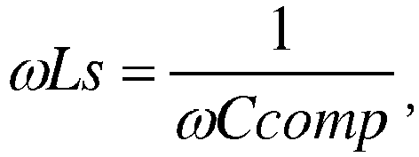
- In one embodiment, the variable impedance device has an inductance Ls and the compensating impedance device comprises a capacitor having a capacitance Ccomp determined in accordance with
- In one embodiment, the coupling device comprises one of a 3dB coupler and a circulator.
- In one embodiment, the impedance device comprises a lumped impedance device.
- In one embodiment, the variable impedance device comprises one of a transistor and a diode.
- In one embodiment, the variable impedance device comprises one of a field effect transistor and a PIN diode.
- According to a second aspect, there is provided a method, comprising: providing an input operable to receive an input signal to be attenuated; providing a coupling device coupled with the input and with an output providing an attenuated input signal; and providing a pair of reflective loads coupled with the coupling device to receive the input signal, each reflective load comprising a first impedance network arranged in parallel with a second impedance network, the first impedance network and the second impedance network each comprising an impedance device and a variable impedance device.
- In one embodiment, each reflective load is coupled at one end with the coupling device to receive the input signal and at another end with ground.
- In one embodiment, the first impedance network and the second impedance network each comprise the impedance device coupled with the coupling device to receive the input signal, the impedance device being coupled with the variable impedance device which is in turn coupled to ground.
- In one embodiment, the first impedance network comprises a series arrangement of a first impedance device and a first variable impedance device, and the second impedance network comprises a series arrangement of a second impedance device and a second variable impedance device.
- In one embodiment, the coupling device has a characteristic impedance Zo, the first and second variable impedance devices have an impedance Z, the first impedance device has an impedance jX1 and the second impedance device has an impedance jX2 determined in accordance with Z = ±X1= ∓X2 = Z0.
- In one embodiment, the first impedance network arranged in parallel with the second impedance network together form a second-order load and each reflective load comprises a parallel arrangement of N' number of the second-order loads, each in series with a further impedance device, where N = 2^ (n-1), n≥ 1.
- In one embodiment, a first second-order load is provided in series with a first further impedance device having an impedance jX1 and a second second-order load is provided in series with a second further impedance device having an impedance jX2 determined in accordance with Z = ±X1= ∓X2 = Z0.
- In one embodiment, the method comprises providing a compensating impedance device provided between each impedance device and variable impedance device.
- In one embodiment, the variable impedance device has an inductance Ls and the compensating impedance device comprises a capacitor having a capacitance Ccomp determined in accordance with

- In one embodiment, the coupling device comprises one of a 3dB coupler and a circulator.
- In one embodiment, the impedance device comprises a lumped impedance device.
- In one embodiment, the variable impedance device comprises one of a transistor and a diode.
- In one embodiment, the variable impedance device comprises one of a field effect transistor and a PIN diode.
- Further particular and preferred aspects are set out in the accompanying independent and dependent claims. Features of the dependent claims may be combined with features of the independent claims as appropriate, and in combinations other than those explicitly set out in the claims.
- Where an apparatus feature is described as being operable to provide a function, it will be appreciated that this includes an apparatus feature which provides that function or which is adapted or configured to provide that function.
- Embodiments of the present invention will now be described further, with reference to the accompanying drawings, in which:
-
Figure 1 illustrates an attenuator; -
Figure 2 illustrates an attenuator according to one embodiment; -
Figure 3 illustrates an equivalent circuit of a PIN diode; -
Figure 4 shows the variation of attenuation of the attenuator ofFigure 1 (junction resistance varies in steps of 5 Ω); and -
Figure 5 shows the variation of attenuation of the attenuator ofFigure 2 (junction resistance varies in steps of 5 Ω). - Before discussing the embodiments in any more detail, first an overview will be provided. Embodiments provide an arrangement which provides for an improved performance attenuator which is achieved using a coupling device coupled with a pair of reflective loads, each reflective load having at least two impedance networks arranged in parallel. The provision of the parallel arrangement of the impedance networks provides for improved dynamic range of the attenuator, whilst retaining essentially an unchanged insertion loss. In particular, embodiments provide a high dynamic range variable attenuator which is of the reflective type for cost effectiveness. In order to provide for further cost reduction and to maintain low insertion losses, the number of 3-dB couplers needs to be kept to a minimum and embodiments utilise just one 3-dB coupler.
-
Figure 2 illustrates a high dynamic range attenuator according to one embodiment. Although this embodiment utilises PIN diodes as the active element, it will be appreciated that field effect transistors (FETs) may equally be utilised and achieve similar results. The arrangement shown inFigure 2 provides a reflective type attenuator which a minimised number of 3-dB couplers. - An input signal is provided over the
path 10 coupled with an input port of the 3-dB coupler 20. The attenuated output signal is provided over thepath 30 coupled with an output port of the 3-dB coupler 20. Also coupled to the 3-dB coupler 20 are a pair of reflective loads 40. Eachreflective load 40 comprises a parallel arrangement of two networks, each comprising a lumped element in series with a PIN diode. In particular, a first network comprises a lumpedelement 50 in series with aPIN diode 60, whilst a second network comprises a lumpedelement 70 in series with aPIN diode 80. The lumpedelements dB coupler 20 whilst thePIN diodes - The performance of the attenuator is optimised by ensuring suitable characteristics for the lumped
elements - The reflection coefficient of the reflective loads of
Figure 2 , can be written as:
Figure 2 can be written as:
- Here, X1 and X2 represent the lumped elements of
Figure 2 . First, it is necessary to impose the condition that the imaginary part of the input impedance is equal to zero, so that the input impedance, Zin, is purely real. Solving equation (4) for Im(Zin) =0 yields the following relationship:
- Using the latter substitution, since it yields a reduced form of the real part of the input impedance, one obtains:

- In order for the circuit of
Figure 2 to achieve a two times greater attenuation range than that offered by the circuit ofFigure 1 , its reflection coefficient given by equation (6) needs to be able to be presented in the form of:
- By imposing that Γ = 0, in equation (6) one obtains a solution in Z :

- The necessary condition for doubling the dynamic range is achieved by requiring that discriminant of equation (8) is equal to zero, yielding the value for the lumped element X1, i.e. X1 = Z0. Once this condition is satisfied, a double zero is achieved at:

- And equation (6) can be re-written as:


Figure 1 . This infers that the dynamic range is doubled without doubling the insertion loss, since there is no insertion loss due to the presence of a second 3-dB coupler. Equation (11) satisfies the two conditions stated earlier. In this way one obtains a variable attenuator solution which satisfies two usually contradicting requirements - cost effectiveness and better performance. - If the circuit of
Figure 1 is denoted as a first order attenuator (since it uses one PIN diode per reflective load), and the circuit ofFigure 2 as a second order since it uses two PIN diodes per reflective load, higher order attenuators can be formed in a similar way presented above, where the allowed orders of the attenuators are determined in the binary exponential fashion. For example, if Rn is identified as the order of the attenuator, the allowed orders of the attenuators are:
- Therefore, the first few allowed orders of attenuators formed in this way are: 1, 2, 4, 8 and so on. The order of the attenuator indicates the amount of increase of its dynamic range. For example, the second order attenuator has a dynamic range that is two times greater than its single order counterpart, and the fourth order attenuator has a dynamic range that is four times greater that its single order counterpart.
-
Figure 3 illustrates the equivalent circuit of a PIN diode. In this figure, LS is the parasitic lead inductance, RS is the parasitic resistance, CP is the parasitic package capacitance, Cj is the parasitic junction capacitance, and RJ is variable junction capacitance. Typical values of the parasitic elements of the PIN diode are: LS=2nH, RS=1.5Ω, CP=0.08pF, Cj=0.12pF while RJ is the current dependent resistor and, ideally, its resistance changes from a perfect open to a perfect short. - The PIN diode's equivalent circuit of
Figure 3 was used to design two attenuators operating at a centre frequency of 2.5 GHz. However, in order to compensate for the large lead inductance (LS=2nH) of the PIN diode ofFigure 3 , a compensating capacitor was added in series with the PIN diode, CCOMP, obtained using the following relationship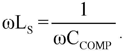
- The first attenuator is a simple, single PIN diode per load design of
Figure 1 , while the second is the design whose topology is given inFigure. 2 . A 3-dB coupler used in the simulations is assumed to have an insertion loss of 0.3 dB (a realistic assumption) and is made to operate in the frequency of 2.3 GHz to 2.7 GHz. The values of the lumped elements, X1 and X2 needed for the attenuator design are obtained using equation (11) to yield C1=1.27 pF and L2=3.16nH. -
Figure 4 represents the variation of attenuation of the attenuator ofFigure 1 , realised with a PIN diode with the equivalent circuit ofFigure 3 . In the equivalent circuit of the PIN diode, it was assumed that the resistance of the junction resistor, RJ varies from 0-50 Ω in steps of 5 Ω. In this case, the maximum insertion loss is about 1.1 dB, while maximum attenuation is about 28 dB and is achieved at 2.7 GHz. The dynamic range of this simple PIN diode-based attenuator varies from 17 dB at 2.3 GHz to 27 dB at 2.7 GHz. - The insertion loss of 1.1 dB of the attenuator of
Figure 1 comprises the losses due to the 3-dB coupler and losses due to the finite resistance of the PIN diode. The insertion loss of a 3-dB coupler is stated to be 0.3 dB, however that applies to a signal travelling in one direction only. In the case of reflective-type configurations, the input signal travels through the 3-dB coupler, reaches the reflective loads and gets reflected off them to travel through the 3-dB coupler again and towards the output port. As such, since the signal travels two times through the 3-dB coupler, its insertion loss is:

-
Figure 5 depicts the attenuation performance of the high dynamic range attenuator ofFigure 2 using the same PIN diode as the simple attenuator ofFigure 1 . The insertion loss of this attenuator is about 1.6 dB, which is in a good agreement with the prediction:
- The maximum attenuation of the attenuator is about 60dB. Its dynamic range varies from over 31 dB (at 2.3 GHz) to over 58 dB (at 2.6 GHz). It is worth noting that the insertion loss of the proposed attenuator, even though increased compared to the single PIN diode case attenuator, is not doubled (since it uses only one 3-dB coupler), while the dynamic range is almost doubled across the indicated frequency range. For comparison, in order to obtain the same dynamic range, a cascade connection of two attenuators of
Figure 1 would be required. However, that would come at the expense of increased insertion loss. The theoretical prediction of the insertion loss in this case is: 2·LOSSsingle_PIN_attenuator + microstrip line loss (0.3-0.4dB) = 2.2+(0.3-0.4) = 2.5-2.6dB which is about 1 dB higher than that of the arrangement ofFigure 2 . - To summarize, the main benefits of embodiments, therefore are: lower insertion loss compared to the case of two attenuators of
Figure 1 connected in cascade, with the same dynamic range - this is due to the fact that only one 3-dB coupler is needed; and lower cost and smaller space required - again, this is due to the fact that only one coupler 3-dB is required which not only improves performance but also leads to a lower cost. - A person of skill in the art would readily recognize that steps of various above-described methods can be performed by programmed computers. Herein, some embodiments are also intended to cover program storage devices, e.g., digital data storage media, which are machine or computer readable and encode machine-executable or computer-executable programs of instructions, wherein said instructions perform some or all of the steps of said above-described methods. The program storage devices may be, e.g., digital memories, magnetic storage media such as a magnetic disks and magnetic tapes, hard drives, or optically readable digital data storage media. The embodiments are also intended to cover computers programmed to perform said steps of the above-described methods.
- The functions of the various elements shown in the Figures, including any functional blocks labelled as "processors" or "logic", may be provided through the use of dedicated hardware as well as hardware capable of executing software in association with appropriate software. When provided by a processor, the functions may be provided by a single dedicated processor, by a single shared processor, or by a plurality of individual processors, some of which may be shared. Moreover, explicit use of the term "processor" or "controller" or "logic" should not be construed to refer exclusively to hardware capable of executing software, and may implicitly include, without limitation, digital signal processor (DSP) hardware, network processor, application specific integrated circuit (ASIC), field programmable gate array (FPGA), read only memory (ROM) for storing software, random access memory (RAM), and non-volatile storage. Other hardware, conventional and/or custom, may also be included. Similarly, any switches shown in the Figures are conceptual only. Their function may be carried out through the operation of program logic, through dedicated logic, through the interaction of program control and dedicated logic, or even manually, the particular technique being selectable by the implementer as more specifically understood from the context.
- It should be appreciated by those skilled in the art that any block diagrams herein represent conceptual views of illustrative circuitry embodying the principles of the invention. Similarly, it will be appreciated that any flow charts, flow diagrams, state transition diagrams, pseudo code, and the like represent various processes which may be substantially represented in computer readable medium and so executed by a computer or processor, whether or not such computer or processor is explicitly shown. The description and drawings merely illustrate the principles of the invention. It will thus be appreciated that those skilled in the art will be able to devise various arrangements that, although not explicitly described or shown herein, embody the principles of the invention and are included within its spirit and scope. Furthermore, all examples recited herein are principally intended expressly to be only for pedagogical purposes to aid the reader in understanding the principles of the invention and the concepts contributed by the inventor(s) to furthering the art, and are to be construed as being without limitation to such specifically recited examples and conditions. Moreover, all statements herein reciting principles, aspects, and embodiments of the invention, as well as specific examples thereof, are intended to encompass equivalents thereof.
Claims (14)
- An attenuator, comprising:an input operable to receive an input signal to be attenuated;a coupling device coupled with said input and with an output providing an attenuated input signal; anda pair of reflective loads coupled with said coupling device to receive said input signal, each reflective load comprising a first impedance network arranged in parallel with a second impedance network, said first impedance network and said second impedance network each comprising an impedance device and a variable impedance device.
- The attenuator of claim 1, wherein each reflective load is coupled at one end with said coupling device to receive said input signal and at another end with ground.
- The attenuator of claim 1 or 2, wherein said first impedance network and said second impedance network each comprise said impedance device coupled with said coupling device to receive said input signal, said impedance device being coupled with said variable impedance device which is in turn coupled to ground.
- The attenuator of any preceding claim , wherein said first impedance network comprises a series arrangement of a first impedance device and a first variable impedance device, and said second impedance network comprises a series arrangement of a second impedance device and a second variable impedance device.
- The attenuator of claim 4, wherein said coupling device has a characteristic impedance Zo, said first and second variable impedance devices have an impedance Z, said first impedance device has an impedance jX1 and said second impedance device has an impedance jX2 determined in accordance with Z = ±X1= ∓TX2 = Z0.
- The attenuator of any preceding claim, wherein said first impedance network arranged in parallel with said second impedance network together form a second-order load and each reflective load comprises a parallel arrangement of N' number of said second-order loads, each in series with a further impedance device, where N = 2^(n-1), n≥ 1.
- The attenuator of any preceding claim, wherein a first second-order load is provided in series with a first further impedance device having an impedance jX1 and a second second-order load is provided in series with a second further impedance device having an impedance jX2 determined in accordance with Z = ±X1= ∓TX2 = Z0.
- The attenuator of any preceding claim, comprising a compensating impedance device provided between each impedance device and variable impedance device.
- The attenuator of any preceding claim, wherein said variable impedance device has an inductance Ls and said compensating impedance device comprises a capacitor having a capacitance Ccomp determined in accordance with

- The attenuator of any preceding claim, wherein said coupling device comprises one of a 3dB coupler and a circulator.
- The attenuator of any preceding claim, wherein said impedance device comprises a lumped impedance device.
- The attenuator of any preceding claim, wherein said variable impedance device comprises one of a transistor and a diode.
- The attenuator of any preceding claim, wherein said variable impedance device comprises one of a field effect transistor and a PIN diode.
- A method, comprising:providing an input operable to receive an input signal to be attenuated;providing a coupling device coupled with said input and with an output providing an attenuated input signal; andproviding a pair of reflective loads coupled with said coupling device to receive said input signal, each reflective load comprising a first impedance network arranged in parallel with a second impedance network, said first impedance network and said second impedance network each comprising an impedance device and a variable impedance device.
Priority Applications (1)
| Application Number | Priority Date | Filing Date | Title |
|---|---|---|---|
| EP14305800.6A EP2950449A1 (en) | 2014-05-28 | 2014-05-28 | Attenuator |
Applications Claiming Priority (1)
| Application Number | Priority Date | Filing Date | Title |
|---|---|---|---|
| EP14305800.6A EP2950449A1 (en) | 2014-05-28 | 2014-05-28 | Attenuator |
Publications (1)
| Publication Number | Publication Date |
|---|---|
| EP2950449A1 true EP2950449A1 (en) | 2015-12-02 |
Family
ID=50942236
Family Applications (1)
| Application Number | Title | Priority Date | Filing Date |
|---|---|---|---|
| EP14305800.6A Withdrawn EP2950449A1 (en) | 2014-05-28 | 2014-05-28 | Attenuator |
Country Status (1)
| Country | Link |
|---|---|
| EP (1) | EP2950449A1 (en) |
Cited By (3)
| Publication number | Priority date | Publication date | Assignee | Title |
|---|---|---|---|---|
| WO2017176814A1 (en) * | 2016-04-04 | 2017-10-12 | Texas Tech University System | 24-ghz low-cost continuous beam steering phased array for indoor smart radar and methods relating thereto |
| CN113629373A (en) * | 2020-05-06 | 2021-11-09 | 中国电信股份有限公司 | Coupler, loop indoor distribution system and signal equalization method |
| AU2020414353B2 (en) * | 2019-12-23 | 2025-01-23 | Raytheon Company | Absorptive phase invariant attenuator |
Citations (7)
| Publication number | Priority date | Publication date | Assignee | Title |
|---|---|---|---|---|
| US3769610A (en) * | 1972-06-15 | 1973-10-30 | Philco Ford Corp | Voltage controlled variable power divider |
| US4902983A (en) * | 1987-02-02 | 1990-02-20 | Nec Corporation | Nonlinear signal generating circuit and nonlinear compensating device using the same |
| US5276411A (en) * | 1992-06-01 | 1994-01-04 | Atn Microwave, Inc. | High power solid state programmable load |
| US6255908B1 (en) * | 1999-09-03 | 2001-07-03 | Amplix | Temperature compensated and digitally controlled amplitude and phase channel amplifier linearizer for multi-carrier amplification systems |
| US20030197559A1 (en) * | 2002-04-23 | 2003-10-23 | Fadhel Ghannouchi | Active predistorting linearizer with agile bypass circuit for safe mode operation |
| US20110057746A1 (en) * | 2009-09-09 | 2011-03-10 | Mitsubishi Electric Corporation | Directional coupler |
| EP2693560A1 (en) * | 2012-08-02 | 2014-02-05 | Alcatel-Lucent | Filter assembly |
-
2014
- 2014-05-28 EP EP14305800.6A patent/EP2950449A1/en not_active Withdrawn
Patent Citations (7)
| Publication number | Priority date | Publication date | Assignee | Title |
|---|---|---|---|---|
| US3769610A (en) * | 1972-06-15 | 1973-10-30 | Philco Ford Corp | Voltage controlled variable power divider |
| US4902983A (en) * | 1987-02-02 | 1990-02-20 | Nec Corporation | Nonlinear signal generating circuit and nonlinear compensating device using the same |
| US5276411A (en) * | 1992-06-01 | 1994-01-04 | Atn Microwave, Inc. | High power solid state programmable load |
| US6255908B1 (en) * | 1999-09-03 | 2001-07-03 | Amplix | Temperature compensated and digitally controlled amplitude and phase channel amplifier linearizer for multi-carrier amplification systems |
| US20030197559A1 (en) * | 2002-04-23 | 2003-10-23 | Fadhel Ghannouchi | Active predistorting linearizer with agile bypass circuit for safe mode operation |
| US20110057746A1 (en) * | 2009-09-09 | 2011-03-10 | Mitsubishi Electric Corporation | Directional coupler |
| EP2693560A1 (en) * | 2012-08-02 | 2014-02-05 | Alcatel-Lucent | Filter assembly |
Non-Patent Citations (1)
| Title |
|---|
| BULJA S ET AL: "A New Structure for Reflection-type Phase Shifter with 360/spl deg/ Phase Control Range", RADAR CONFERENCE, 2005. EURAD 2005. EUROPEAN OCT. 6, 2005, PISCATAWAY, NJ, USA,IEEE, 6 October 2005 (2005-10-06), pages 339 - 342, XP010910885, ISBN: 978-2-9600551-3-9, DOI: 10.1109/EURAD.2005.1605629 * |
Cited By (7)
| Publication number | Priority date | Publication date | Assignee | Title |
|---|---|---|---|---|
| WO2017176814A1 (en) * | 2016-04-04 | 2017-10-12 | Texas Tech University System | 24-ghz low-cost continuous beam steering phased array for indoor smart radar and methods relating thereto |
| WO2017176816A3 (en) * | 2016-04-04 | 2019-04-25 | Texas Tech University System | 24-ghz low-cost continuous beam steering phased array for indoor smart radar and methods relating thereto |
| US11735828B2 (en) | 2016-04-04 | 2023-08-22 | Texas Tech University System | 24-GHz low-cost continuous beam steering phased array for indoor smart radar and methods relating thereto |
| AU2020414353B2 (en) * | 2019-12-23 | 2025-01-23 | Raytheon Company | Absorptive phase invariant attenuator |
| AU2020414353C1 (en) * | 2019-12-23 | 2025-04-17 | Raytheon Company | Absorptive phase invariant attenuator |
| CN113629373A (en) * | 2020-05-06 | 2021-11-09 | 中国电信股份有限公司 | Coupler, loop indoor distribution system and signal equalization method |
| CN113629373B (en) * | 2020-05-06 | 2022-11-01 | 中国电信股份有限公司 | Coupler, loop indoor distribution system and signal equalization method |
Similar Documents
| Publication | Publication Date | Title |
|---|---|---|
| US4028632A (en) | Power dividing and combining techniques for microwave amplifiers | |
| US10784557B2 (en) | Signal processing circuit, signal processing module, and communication apparatus | |
| US9509252B2 (en) | Doherty amplifier | |
| US7990237B2 (en) | System and method for improving performance of coplanar waveguide bends at mm-wave frequencies | |
| US8193857B1 (en) | Wideband doherty amplifier circuit | |
| JP2025500102A (en) | High bandwidth load modulated power amplifier and corresponding RF front-end module - Patents.com | |
| KR101946187B1 (en) | 3-Way Sequential Power Amplifier | |
| EP2544369B1 (en) | Attenuator | |
| US6252474B1 (en) | Semiconductor phase shifter having high-pass signal path and low-pass signal path connected in parallel | |
| US20090286492A1 (en) | Rf switch and transmit and receive module comprising such a switch | |
| US11689189B2 (en) | Digital phase shifter | |
| US7295090B2 (en) | Filter circuit | |
| KR20210140770A (en) | Power distributor, regulation method, power distribution method, storage medium and electronic device | |
| CN112671372B (en) | Electronically controlled digital phase shifter and control method thereof | |
| US20200244240A1 (en) | Wideband distributed power amplifiers and systems and methods thereof | |
| US6066992A (en) | Variable ISO attenuator using absorptive/reflective elements and latching | |
| US11705868B2 (en) | System for adapting the voltage of a drain of a power stage | |
| EP3089365A1 (en) | Directional device for phase shifting and attenuating signals | |
| Mabrouki et al. | A 4 bits Reflection type phase shifter based on Ga As FET | |
| KR101319266B1 (en) | Transistor Amplifing circuit and power amplifier applying the same | |
| EP4082110B1 (en) | Absorptive phase invariant attenuator | |
| US20100182092A1 (en) | Power sensitive variable attenuator | |
| EP2996190A1 (en) | Method for selecting a phase shift, phase shifter, beamformer and antenna array | |
| Figur et al. | RF-MEMS multi-mode-matching networks for GaN power transistors | |
| CN119254169A (en) | An adaptive limiter and a limiting method thereof |
Legal Events
| Date | Code | Title | Description |
|---|---|---|---|
| AK | Designated contracting states |
Kind code of ref document: A1 Designated state(s): AL AT BE BG CH CY CZ DE DK EE ES FI FR GB GR HR HU IE IS IT LI LT LU LV MC MK MT NL NO PL PT RO RS SE SI SK SM TR |
|
| AX | Request for extension of the european patent |
Extension state: BA ME |
|
| PUAI | Public reference made under article 153(3) epc to a published international application that has entered the european phase |
Free format text: ORIGINAL CODE: 0009012 |
|
| 17P | Request for examination filed |
Effective date: 20160602 |
|
| RBV | Designated contracting states (corrected) |
Designated state(s): AL AT BE BG CH CY CZ DE DK EE ES FI FR GB GR HR HU IE IS IT LI LT LU LV MC MK MT NL NO PL PT RO RS SE SI SK SM TR |
|
| 17Q | First examination report despatched |
Effective date: 20170419 |
|
| STAA | Information on the status of an ep patent application or granted ep patent |
Free format text: STATUS: THE APPLICATION IS DEEMED TO BE WITHDRAWN |
|
| 18D | Application deemed to be withdrawn |
Effective date: 20171031 |