EP2950391A1 - Antenna - Google Patents
Antenna Download PDFInfo
- Publication number
- EP2950391A1 EP2950391A1 EP14743067.2A EP14743067A EP2950391A1 EP 2950391 A1 EP2950391 A1 EP 2950391A1 EP 14743067 A EP14743067 A EP 14743067A EP 2950391 A1 EP2950391 A1 EP 2950391A1
- Authority
- EP
- European Patent Office
- Prior art keywords
- resonance
- area
- radiation
- end portion
- axial direction
- Prior art date
- Legal status (The legal status is an assumption and is not a legal conclusion. Google has not performed a legal analysis and makes no representation as to the accuracy of the status listed.)
- Granted
Links
Images






Classifications
-
- H—ELECTRICITY
- H01—ELECTRIC ELEMENTS
- H01Q—ANTENNAS, i.e. RADIO AERIALS
- H01Q1/00—Details of, or arrangements associated with, antennas
- H01Q1/36—Structural form of radiating elements, e.g. cone, spiral, umbrella; Particular materials used therewith
- H01Q1/38—Structural form of radiating elements, e.g. cone, spiral, umbrella; Particular materials used therewith formed by a conductive layer on an insulating support
-
- H—ELECTRICITY
- H01—ELECTRIC ELEMENTS
- H01Q—ANTENNAS, i.e. RADIO AERIALS
- H01Q1/00—Details of, or arrangements associated with, antennas
- H01Q1/48—Earthing means; Earth screens; Counterpoises
-
- H—ELECTRICITY
- H01—ELECTRIC ELEMENTS
- H01Q—ANTENNAS, i.e. RADIO AERIALS
- H01Q9/00—Electrically-short antennas having dimensions not more than twice the operating wavelength and consisting of conductive active radiating elements
- H01Q9/04—Resonant antennas
- H01Q9/30—Resonant antennas with feed to end of elongated active element, e.g. unipole
- H01Q9/40—Element having extended radiating surface
Definitions
- the present invention relates to an antenna provided with an unbalanced power supply member, a resonance conductor, a grounding conductor and a radiation conductor.
- An antenna 100 illustrated in Figure 15 is disclosed, the antenna 100 including an unbalanced power supply member having an outer conductor and an inner conductor as with a coaxial cable, and a plate like non-power supply element whose planar shape is molded in an H shape (see Patent Literature 1).
- the antenna 100 of Patent Literature 1 includes the unbalanced power supply member 111, a resonance conductor 112, a grounding conductor 113 and a power supply element 114.
- the resonance conductor 112 is formed with first and second resonance conductors 120a and 120b extending forward in an axial direction of the unbalanced power supply member 111 in parallel to a power supply unit 118.
- the grounding conductor 113 is formed with a fixing portion 125 electrically connected to the unbalanced power supply member 111, and first and second grounding conductors 126a and 126b extending backward in the axial direction from the first and second resonance conductors 120a and 120b in parallel to a non-power supply unit 119.
- the power supply element 114 has a predetermined area, extends forward in the axial direction, and is electrically connected to a central conductor 115 of the unbalanced power supply member 111 which constitutes the power supply unit 118.
- Patent Literature 1 Japanese Patent Laid-Open No. 2012-195713
- the antenna 100 disclosed in Patent Literature 1 can provide a wideband and high gain and can freely and finely adjusts a use frequency band.
- a use frequency is approximately 2.0 GHz to approximately 4.0 GHz, and a VSWR (voltage standing wave ratio) is 2 or less.
- a lower limit frequency can neither be lowered to a lower frequency band (for example, 700 MHz) in a state where a wide band is maintained while a size of the antenna is kept small, nor the VSWR can be made 2 or less in a full band.
- An object of the present invention is to provide an antenna which is capable of transmitting or receiving a radio wave in the full band among frequency bands (fractional bandwidth) which can be used, and the antenna which can be used in a wide band.
- Another object of the present invention is to provide an antenna which is capable of transmitting or receiving a radio wave in a wide frequency band, which can provide a high gain in a band between 700 MHz and 3.2 GHz, and which has a VSWR of 2 or less in a state where a size of the antenna is kept small.
- An antenna according to the present invention for solving the above-described problem includes a dielectric substrate having predetermined permittivity and having first and second regions sectioned by a central axial line dividing a width dimension, an unbalanced power supply member located on the central axial line and having a non-power supply unit and a power supply unit, the non-power supply unit extending in an axial direction and having predetermined length, and the power supply unit extending forward in the axial direction from the non-power supply unit, a resonance conductor molded into a plate shape having a predetermined area and fixed on one face of the dielectric substrate, a grounding conductor molded into a plate shape having a predetermined area, fixed on one face of the dielectric substrate and continuously coupled to the resonance conductor, and a radiation conductor molded into a plate shape having a predetermined area, fixed on one face of the dielectric substrate, and electrically connected to the power supply unit, and the resonance conductor has a connection area electrically connected to the unbalanced power supply member, a first
- the radiation stepped portions formed at the first rear end portion of the second radiation area and the radiation stepped portions formed at the second rear end portion of the second radiation area have a first radiation stepped portion located at a side of the central axial line and denting forward in the axial direction from the first and second rear end portions, a second radiation stepped portion located outward in a width direction of the first radiation stepped portion and denting forward in the axial direction from the first radiation stepped portion, and a third radiation stepped portion located outward in a width direction of the second radiation stepped portion and tilting so as to gradually separate from the central axial line.
- a plurality of resonance stepped portions denting stepwise backward in the axial direction toward outward in the width direction from the central axial line are formed at the front end portion of the first resonance area, and a plurality of resonance stepped portions denting stepwise backward in the axial direction toward outward in the width direction from the central axial line are formed at the front end portion of the second resonance area.
- the resonance stepped portions formed at the front end portion of the first resonance area and the resonance stepped portions formed at the front end portion of the second resonance area have a first resonance stepped portion located at a side of the central axial line and denting backward in the axial direction from the front end portions of the resonance areas, a second resonance stepped portion located outward in a width direction of the first resonance stepped portion and denting backward in the width direction from the first resonance stepped portion, and a third resonance stepped portion located outward in a width direction of the second resonance stepped portion and denting backward in the axial direction from the second resonance stepped portion.
- a plurality of attenuating stepped portions denting stepwise forward in the axial direction toward outward in the width direction from the central axial line are formed at a rear end portion of the first ground area, and a plurality of attenuating stepped portions denting stepwise forward in the axial direction toward outward in the width direction from the central axial line are formed at the rear end portion of the second ground area.
- the attenuating stepped portions formed at the rear end portion of the first ground area and the attenuating stepped portions formed at the rear end portion of the second ground area have a first attenuating stepped portion located at a side of the central axial line and denting forward in the axial direction from the rear end portions of the resonance areas and a second attenuating stepped portion located outward in a width direction of the first attenuating stepped portion and denting forward in the axial direction from the first attenuating stepped portion.
- a first slit located near the radiation stepped portions and extending so as to gradually separate from the central axial line toward forward in the axial direction is formed, or a plurality of first through holes located near the radiation stepped portions and aligned so as to gradually separate from the central axial line toward forward in the axial direction are formed
- a second slit located near the radiation stepped portions and extending so as to gradually separate from the central axial line toward forward in the axial direction is formed, or a plurality of second through holes located near the radiation stepped portions and aligned so as to gradually separate from the central axial line toward forward in the axial direction are formed.
- a third slit located near the resonance stepped portions and extending so as to gradually separate from the central axial line toward backward in the axial direction is formed, or a plurality of third through holes located near the resonance stepped portions and aligned so as to gradually separate from the central axial line toward backward in the axial direction are formed
- a fourth slit located near the resonance stepped portions and extending so as to gradually separate from the central axial line toward backward in the axial direction is formed, or a plurality of fourth through holes located near the resonance stepped portions and aligned so as to gradually separate from the central axial line toward backward in the axial direction are formed.
- a first void portion where the dielectric substrate does not exist is formed between the front end portion of the first resonance area and the first rear end portion of the second radiation area
- a second void portion where the dielectric substrate does not exist is formed between the front end potion of the second resonance area and the second rear end portion of the second radiation area.
- the first resonance area located in the first region and the second resonance area located in the second region are symmetric with respect to the central axial line
- the first ground area located in the first region and the second ground area located in the second region are symmetric with respect to the central axial line
- the first and the second radiation areas located in the first region and the first and the second radiation areas located in the second region are symmetric with respect to the central axial line.
- the unbalanced power supply member is formed with a first conductor extending in the axial direction, an insulator covering an outer periphery of the first conductor, and a second conductor covering an outer periphery of the insulator and extending in the axial direction
- the non-power supply unit is formed with the first and the second conductors and the insulator
- the power supply unit is formed with the first conductor
- the connection area of the resonance conductor is electrically connected to the second conductor.
- a length dimension in the axial direction of the grounding conductor falls within a range between 10 and 15 cm, and is set at length of approximately 1/4 wavelength of 700 MHz.
- an antenna because a plurality of radiation stepped portions which dent stepwise forward in the axial direction are formed at the first and the second rear end portions of the second radiation area, a high frequency current of substantially the same direction flows between the plurality of radiation stepped portions of the first and the second rear end portions of the second radiation area and the front end potions of first and second resonance areas of the resonance conductor, the radiation stepped portions of the second radiation area fixed at the dielectric substrate having predetermined permittivity and the front end portions of the first and the second resonance areas resonate at a plurality of points via the high frequency current of substantially the same direction, a high frequency current induced at the first radiation area fixed at the dielectric substrate and a high frequency current induced at the first and the second resonance areas resonate, while a high frequency current induced at the first and the second ground areas of the grounding conductor fixed at the dielectric substrate and a high frequency current induced at the non-power supply unit resonate, so that it is possible to obtain a plurality of resonance frequencies of different bands.
- the antenna can obtain a plurality of resonance frequencies of different bands, and because the obtained plurality of resonance frequencies are continuously adjacent to each other, and the resonance frequencies partly overlap with each other, it is possible to drastically expand a use frequency band at the antenna.
- the antenna can obtain a high gain whose VSWR (voltage standing wave ratio) is 2 or less, and can transmit or receive a radio wave in a full band among frequency bands (fractional bandwidths) which can be used, and the antenna can be used in a wide band, and can transmit or receive a radio wave of a wide band only with one antenna.
- a high frequency current of substantially the same direction flows between the first to the third radiation stepped portions of the first and the second rear end portions of the second radiation area and the front end portions of the first and the second resonance areas of the resonance conductor, the first to the third radiation stepped portions and the front end portions of the first and the second resonance areas resonate at a plurality of points via the high frequency current of substantially the same direction, a high frequency current induced at the first radiation area and a high frequency current induced at the first and the second resonance areas resonate, while a high frequency current induced at the first and the second ground areas and a high frequency current induced at the non-power supply unit resonate, so that it is possible to obtain a
- a high frequency current of substantially the same direction flows between the plurality of radiation stepped portions of the second radiation area and the plurality of resonance stepped portions of the first and the second resonance areas
- the radiation stepped portions and the resonance stepped portions resonate at a plurality of points via the high frequency current of substantially the same direction
- a high frequency current induced at the first radiation area and a high frequency current induced at the first and the second resonance areas resonate, while a high frequency current induced at the first and the second ground areas and a high frequency current induced at the non-power supply unit resonate, so that it is possible to obtain a plurality of resonance frequencies of different bands.
- the antenna can secure a wide use frequency band.
- a high frequency current of substantially the same direction flows between the first to the third radiation stepped portions of the first and the second rear end portions of the second radiation area and the first to the third resonance stepped portions of the front end portions of the first and the second resonance areas, the first to the third radiation stepped portions and the first to the third resonance stepped portions resonate at a plurality of points via the high frequency current of substantially the same direction, a high frequency current induced at the first radiation area and a high frequency current induced at the first and the second resonance areas resonate, while a high frequency current induced at the first and the second ground areas and a high frequency current induced at the non-power supply unit resonate, so that it is possible to obtain a plurality of resonance frequencies of
- the antenna in which the plurality of attenuating stepped portions are formed at the rear end portion of the first ground area and the plurality of attenuating stepped portions are formed at the rear end portion of the second ground area, when a high frequency current flows at the rear end portions of the first and the second ground areas, although the high frequency current flows through a chassis and a connection cable of a transceiver connected to the antenna, which affects and changes a radiation pattern of a radio wave and a gain at the antenna, because it is possible to attenuate or block the radio wave by the plurality of attenuating stepped portions formed at the rear end portions of the first and the second ground areas, the high frequency current does not flow through the chassis and the connection cable of the transceiver, so that it is possible to prevent change of the radiation pattern of the radio wave and the gain and secure a radiation pattern and a gain at the antenna as designed.
- the attenuating stepped portions of the first and the second ground areas have the first attenuating stepped portion located at a side of the central axial line, and the second attenuating stepped portion located outward in the width direction of the first attenuating stepped portion, because it is possible to attenuate or block a radio wave by the first and the second attenuating stepped portions formed at the rear end portions of the first and the second ground areas, a high frequency current does not flow through the chassis and the connection cable of the transceiver, so that it is possible to prevent change of the radiation pattern of the radio wave and the gain at the antenna and secure a radiation pattern and a gain at the antenna as designed.
- the antenna in which the first slit or the plurality of first through holes located near the radiation stepped portion is formed at the dielectric substrate which extends between the front end portion of the first resonance area and the first rear end portion of the second radiation area, and the second slit or the plurality of second through holes located near the radiation stepped portion is formed at the dielectric substrate which extends between the front end portion of the second resonance area and the second rear end portion of the second radiation area, because slits or through holes located near the radiation stepped portion are formed at the dielectric substrate, coupling capacitance of the dielectric substrate which extends between the front end portions of the first and the second resonance areas and the first and the second rear end portions of the second radiation area can be reduced, so that it is possible to reduce a rate at which heat is dissipated instead of a radio wave being generated, and drastically improve tan ⁇ as an element of radio wave conversion efficiency at the antenna. As a result of slits or through holes being formed at the dielectric substrate near the radiation stepped portion, the antenna can increase
- the antenna in which the third slit or the plurality of third through holes located near the resonance stepped portion is formed at the dielectric substrate which extends between the front end potion of the first resonance area and the first rear end portion of the second radiation area, and the fourth slit or the plurality of fourth through holes located near the resonance stepped portion is formed at the dielectric substrate which extends between the front end portion of the second resonance area and the second rear end portion of the second radiation area, because slits or through holes located near the resonance stepped portion are formed at the dielectric substrate, coupling capacitance of the dielectric substrate which extends between the front end portions of the first and the second resonance areas and the first and the second rear end portions of the second radiation area can be reduced, so that it is possible to reduce a rate at which heat is dissipated instead of a radio wave being generated, and drastically improve tan ⁇ as an element of radio wave conversion efficiency at the antenna. As a result of slits or through holes being formed at the dielectric substrate near the resonance stepped portion, the antenna can increase
- the antenna in which the first void portion where the dielectric substrate does not exist is formed between the front end portion of the first resonance area and the first rear end portion of the second radiation area, and the second void portion where the dielectric substrate does not exist is formed between the front end portion of the second resonance area and the second rear end portion of the second radiation area, because the first and the second void portions where the dielectric substrate does not exist are respectively formed between the front end portion of the first resonance area and the first rear end portion of the second radiation area, and between the front end portion of the second resonance area and the second rear end portion of the second radiation area, coupling capacitance between the front end portions of the first and the second resonance areas and the first and the second rear end portions of the second radiation area can be drastically reduced, so that it is possible to reduce a rate at which heat is dissipated instead of a radio wave being generated, and drastically improve tan ⁇ as an element of radio wave conversion efficiency at the antenna.
- the antenna can increase a radiation gain and can emit a radio
- the first resonance area located in the first region and the second resonance area located in the second region are symmetric with respect to the central axial line
- the first ground area located in the first region and the second ground area located in the second region are symmetric with respect to the central axial line
- the first and the second radiation areas located in the first region and the first and the second radiation areas located in the second region are symmetric with respect to the central axial line
- the first and the second radiation areas located in the first region and the first and the second radiation areas located in the second region are made symmetric with respect to the central axial line
- the first and the second resonance areas, the first and the second ground areas, and the first and the second radiation areas being disposed so as to be symmetric with respect to the central axial line
- the first and the second rear end portions of the second radiation area and the front end portions of the first and the second resonance areas of the resonance conductor resonate at a plurality of points at substantially the same coupling capacitance
- the first radiation area and the first and the second resonance areas resonate
- the first and the second ground areas of the grounding conductor and the non-power supply unit resonate at substantially the same coupling capacitance, so that the antenna can obtain a plurality of resonance frequencies of different bands and secure a wide use frequency band.
- the non-power supply unit is formed with the first and the second conductors and the insulating body, and the connection area of the resonance conductor is electrically connected to the second conductor, the second radiation area and the first and the second resonance areas resonate at a plurality of points, and the first radiation area and the first and the second resonance areas resonate, so that the antenna can obtain a plurality of resonance frequencies of different bands and can secure a wide use frequency band.
- the antenna can stably maintain impedance, can prevent a short circuit between the first conductor and the second conductor of the unbalanced power supply member, and can prevent breakage of a high frequency circuit of the transceiver due to a short circuit between the conductors.
- the length dimension in the axial direction of the grounding conductor falls within a range between 10 and 15 cm and is set at length of approximately 1/4 wavelength of 700 MHz
- the length dimension in the axial direction of the grounding conductor falls within the above-described range
- the length dimension becomes length of approximately 1/4 wavelength of 700 MHz
- a use frequency band at the antenna can be made to fall within a range of 700 MHz and 3.2 GHz, so that it is possible to lower a lower limit frequency to 700 MHz while the size of the antenna is kept small.
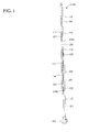
- Figure 1 is a plan view of an antenna 10A illustrated as one example.
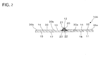
- Figure 2 is a cross-sectional diagram cut along line 2-2 in Figure 1
- Figure 3 is a cross-sectional diagram cut along line 3-3 in Figure 1.
- Figure 1 illustrates an axial direction with an arrow A, a width direction with an arrow B, forward in the axial direction i with an arrow A1, and backward in the axial direction with an arrow A2.
- Figure 1 illustrates a central axial line S1 with a dashed-dotted line.
- the antenna 10A is comprised of a dielectric substrate 11 (print circuit board) having predetermined permittivity and an unbalanced power supply member 12 (a coaxial cable or a semi-rigid cable), a resonance conductor 13 and a grounding conductor 14, and a radiation conductor 15.
- the dielectric substrate 11 is formed with glass epoxy having predetermined permittivity.
- the dielectric substrate 11 can be also formed with a thermoplastic synthetic resin or a thermosetting synthetic resin having predetermined permittivity, or a ceramic substrate, other than glass epoxy
- the dielectric substrate 11 which has a plate shape having predetermined thickness, is molded so that the planar shape of the dielectric substrate 11 is a rectangle which is elongated in the axial direction.
- the dielectric substrate 11 has an upper face 16 (one face) and a lower face 17 (the other face), and has a first region 18 and a second region 19 sectioned by the central axial line S1 which divides a width direction of the dielectric substrate 11.
- the dielectric substrate 11 serves as a capacitor in which electric charge is accumulated at the antenna 10A.
- a length dimension in the axial direction, a length dimension in the width direction, and a thickness dimension between the upper face 16 and the lower face 17 of the dielectric substrate 11 are not particularly limited and are freely designed, so that a frequency bandwidth can be freely adjusted.
- the unbalanced power supply member 12 is located on the central axial line S1 on the upper face 16 of the dielectric substrate 11, has predetermined length and extends in the axial direction. As illustrated in Figures 1 and 2 , the unbalanced power supply member 12 is comprised of a rod-like elongated first conductor 20 (central metal conductor), an insulating body 21 which has a circular cross section and which covers an outer periphery of the first conductor 20, and a second conductor 22 (external metal conductor) which has a cylindrical cross section and which covers an outer periphery of the insulating body 21.
- an outer periphery of the first conductor 20 is fixedly attached to an inner periphery of the insulating body 21, and an outer periphery of the insulating body 21 is fixedly attached to an inner periphery of the second conductor 22.
- the unbalanced power supply member 12 has a non-power supply unit 23 which is set to have predetermined length (approximately ⁇ /4) and which vertically extends in the axial direction, and a power supply unit 24 which extends forward in the axial direction from the non-power supply unit 23.
- a connector 25 is attached to a rear end of the unbalanced power supply member 12.
- the non-power supply unit 23 is comprised of the first conductor 20, the insulating body 21 and the second conductor 22.
- the power supply unit 24 is comprised of the first conductor 20.
- a conductive metal such as gold, nickel, copper and silver can be used as the first conductor 20 and the second conductor 22, and thermoplastic synthetic resin (particularly, polytetrafluoroethylene having plastic permittivity) which becomes a material for fixing impedance of the unbalanced power supply member 12 can be used as the insulating body 21.
- the resonance conductor 13 is formed with a conductive metal (such as gold, nickel, copper and silver) and is molded in a plate shape having a predetermined area.
- the resonance conductor 13 is fixed on the upper face of the dielectric substrate 11.
- the resonance conductor 13 has a connection area 26 electrically connected to the unbalanced power supply member 12, a first resonance area 27 located in the first region 18 of the dielectric substrate 11, and a second resonance area 28 located in the second region 19 of the dielectric substrate 11.
- connection area 26 extends in a width direction across the central axial line S1.
- a periphery of the second conductor 22 of the unbalanced power supply member 12 abuts on the connection area 26, and the second conductor 20 is electrically connected (fixed) to the connection area 26 through molding (such as soldering) (fixing means).
- the first resonance area 27 is coupled to the connection area 26, and extends in the axial direction while separating outward in the width direction from the central axial line S1 (first radiation area of a radiation conductor which will be described later) by a predetermined dimension.
- the second resonance area 28 is coupled to the connection area 26, and extends in the axial direction while separating outward in the width direction from the central axial line S1 (first radiation area of the radiation conductor) by a predetermined dimension.
- the connection area 26 and the first and the second resonance areas 27 and 28 are fixed on the upper face 16 of the dielectric substrate 11.
- the first resonance area 27 and the second resonance area 28 are shaped in a rectangle which has a predetermined width dimension and which is elongated in the axial direction, and have planar shapes of the same shape and the same size, which are symmetric with respect to the central axial line S1.
- the first resonance area 27 has a first front end portion 29a extending in the width direction, and a first inner portion 30a and a first outer portion 31 a extending in the axial direction
- the second resonance area 28 has a second front end portion 29b extending in the width direction, and a second inner portion 30b and a second outer portion 31b extending in the axial direction.
- the front end portions 29a and 29b have the same length dimension in the width direction
- the inner portions 30a and 30b have the same length dimension in the axial direction
- the outer portions 31a and 31b have the same length direction in the axial direction.
- the inner portions 30a and 30b have the same first separation dimension from the central axial line S1 (the first radiation area 37 of the radiation conductor 15), and the inner portions 30a and 30b are in parallel with respect to the central axial line S1 (the first radiation area 37).
- the grounding conductor 14 which is formed with a conductive metal (such as gold, nickel, copper and silver), is molded in a plate shape having a predetermined area, and continuously coupled to the resonance conductor 13 (integrally formed with the resonance conductor 13).
- the grounding conductor 14 is fixed on the upper face 16 of the dielectric substrate 11.
- the grounding conductor 14 has a first ground area 32 located in the first region 18 of the dielectric substrate 11, and a second ground area 33 located in the second region 19 of the dielectric substrate 11.
- the first ground area 32 is coupled to the first resonance area 27 and extends backward in the axial direction from the first resonance area 27 while separating outward in the width direction from the central axial line S1 (unbalanced power supply member 12) by a predetermined dimension.
- the second ground area 33 is coupled to the second resonance area 28 and extends backward in the axial direction from the second resonance area 28 while separating outward in the width direction from the central axial line S1 (unbalanced power supply member 12) by a predetermined dimension.
- the first ground area 32 and the second ground area 33 are fixed on the upper face 16 of the dielectric substrate 11.
- the first ground area 32 and the second ground area 33 are shaped in a rectangle which has a predetermined width dimension and which is elongated in the axial direction, and have planar shapes of the same shape and the same size, which are symmetric with respect to the central axial line S1.
- the first ground area 32 has a first rear end portion 34a extending in the width direction, and a first inner portion 35a and a first outer portion 36a extending in the axial direction
- the second ground area 33 has a second rear end portion 34b extending in the width direction, and a second inner portion 35b and a second outer portion 36b extending in the axial direction.
- the rear end portions 34a and 34b have the same length dimension in the width direction
- the inner portions 35a and 35b have the same length dimension in the axial direction
- the outer portions 36a and 36b have the same length dimension in the axial direction.
- the inner portions 35a and 35b have the same second separation dimension from the central axial line S1 (unbalanced power supply member 12), and the inner portions 35a and 35b are in parallel with respect to the central axial line S1 (unbalanced power supply member 12).
- the radiation conductor 15 which is formed with a conductive metal (such as gold, nickel, copper and silver), is molded in a plate shape having a predetermined area, and fixed on the upper face 16 of the dielectric substrate 11.
- the radiation conductor 15 has a first radiation area 37 which is located between the first and the second resonance areas 27 and 28 and which extends forward in the axial direction from the connection area 26, and a second radiation area 38 which extends forward in the axial direction from a front end portion 39 of the first radiation area 37.
- the first and the second radiation areas 37 and 38 are integrally formed.
- the first radiation area 37 is located between the first and the second resonance areas 27 and 28 of the resonance conductor 13.
- the first radiation area 37 has a rectangular shape which has a predetermined width dimension and which is elongated in the axial direction, and is fixed on the upper face 16 of the dielectric substrate 11.
- the area 37 located in the first region 18 of the dielectric substrate 11 and the area 37 located in the second region 19 of the dielectric substrate 11 are symmetric with respect to the central axial line S1.
- the rear end portion 40 of the first radiation area 37 is electrically connected to the power supply unit 24 of the unbalanced power supply member 12.
- the second radiation area 38 separates forward in the axial direction from the first and the second front end portions 29a and 29b of the first and the second resonance areas 27 and 28 by a predetermined dimension and is fixed on the upper face 16 of the dielectric substrate 11.
- the second radiation area 38 has a larger width dimension than a width dimension of the first radiation area 37.
- the area 38 located in the first region 18 of the dielectric substrate 11 and the area 38 located in the second region 19 of the dielectric substrate 11 are symmetric with respect to the central axial line S1.
- a plurality of radiation stepped portions 42 which dent stepwise forward in the axial direction toward outward of the width direction from the central axial line S1 (which distend stepwise backward in the axial direction toward the central axial line S1 from both side portions of the area 38) are formed.
- the radiation stepped portions 42 include a first radiation stepped portion 42a which is located at a side of the central axial line S1 and which dents forward in the axial direction from the first rear end portion 41, a second radiation stepped portion 42b which is located outward in a width direction of the first radiation stepped portion 42a and which dents forward in the axial direction from the first radiation stepped portion 42a, and a third radiation stepped portion 42c which is located outward in a width direction of the second radiation stepped portion 42b and which tilts so as to gradually separate from the central axial line S1. It should be noted that the number of radiation stepped portions 42 is not limited to three, and four or more stepped radiation portions 42 may be formed.
- a plurality of radiation stepped portions 44 which dent stepwise forward in the axial direction toward outward in the width direction from the central axial line S1 (which distend stepwise backward in the axial direction toward the central axial line S1 from both side portions of the area 38) are formed.
- the radiation stepped portions 44 include a first radiation stepped portion 44a which is located at a side of the central axial line S1 and which dents forward in the axial direction from the second rear end portion 43, a second radiation stepped portion 44b which is located outward in a width direction of the first radiation stepped portion 44a and which dents forward in the axial direction from the first radiation stepped portion 44a, and a third radiation stepped portion 44c which is located outward in a width direction of the second radiation stepped portion 44b and which tilts so as to gradually separate from the central axial line S1. It should be noted that the number of the radiation stepped portions 44 is not limited to three, and four or more radiation stepped portions 44 may be formed.
- a separation dimension in the axial direction between the first and the second front end portions 29a and 29b of the first and the second resonance areas 27 and 28 and the first radiation stepped portions 42a and 44a is greater than a separation dimension in the axial direction between the first and the second front end portions 29a and 29b of the first and the second resonance areas 27 and 28 and the first and the second rear end portions 41 and 43 of the second radiation area 38, and a separation dimension in the axial direction between the first and the second front end portions 29a and 29b and the second radiation stepped portions 42b and 44b is greater than a separation dimension in the axial direction between the first and the second front end portions 29a and 29b and the first radiation stepped portions 42a and 44a.
- a separation dimension in the axial direction between the first and the second front end portions 29a and 29b and the third radiation stepped portions 42c and 44c is greater than a separation dimension in the axial direction between the first and the second front end portions 29a and 29b and the second radiation stepped portions 42b and 44b.
- the dielectric substrate 11 having predetermined permittivity serves as a dielectric body, a high frequency current of substantially the same direction flows between the first to the third radiation stepped portions 42a to 42c of the first rear end portion 41 of the second radiation area 38 and the first front end portion 29a of the first resonance area 27, and the first to the third radiation stepped portions 42a to 42c and the first front end portion 29a resonate at a plurality of points via the high frequency current of substantially the same direction, while a high frequency current of substantially the same direction flows between the first to the third radiation stepped portions 44a to 44c of the second rear end portion 43 of the second radiation area 38 and the second front end portion 29b of the second resonance area 28, and the first to the third radiation stepped portions 44a to 44c and the second front end portion 29b resonate at a plurality of points via the high frequency current of substantially the same direction.
- a high frequency current induced at the first and the second front end portions 29a and 29b of the first and the second resonance areas 27 and 28 and a high frequency current induced at the first and the second rear end portions 41 and 43 of the second radiation area 38 resonate, while a high frequency current induced at the second resonance areas 27 and 28 (first and the second inner portions 30a and 30b) and a high frequency current induced at the first radiation area 37 resonate.
- the antenna 10A can obtain a plurality of resonance frequencies of different bands. Because the antenna 10A can obtain a plurality of resonance frequencies of different bands, and the obtained plurality of resonance frequencies are continuously adjacent to each other and partly overlap with each other, it is possible to drastically expand a use frequency band at the antenna 10A.
- the antenna 10A can achieve a VSWR of 2 or less, and can transmit or receive a radio wave in a full band among frequency bands (fractional bandwidths) which can be used, and the antenna can be used in a wide band, and can transmit or receive a radio wave of a wide band only with one antenna.
- a separation dimension between the first and the second inner portions 30a and 30b of the first and the second resonance areas 27 and 28, and the central axial line S1 falls within a range between 0.5 and 1.0 mm, while a separation dimension between the first and the second inner portions 35a and 35b of the first and the second ground areas 32 and 33, and the central axial line S1 falls within a range between 1.9 and 10 mm. If these separation dimensions exceed the above-described ranges, saturation occurs in a state where the antenna 10A can use the widest frequency band, and the frequency band of the antenna 10A cannot be expanded wider. By changing these separation dimensions within the above-described ranges, it is possible to adjust a use frequency band to be wider or narrower, so that it is possible to stabilize a resonance band.
- the antenna 10A can achieve optimal resonance efficiency of a radio wave by these separation dimensions being set to fall within the above-described ranges, so that it is possible to make the second radiation area 38 and the first and the second resonance areas 27 and 28 resonate efficiently at a plurality of points, while it is possible to make the first and the second resonance areas 27 and 28 and the first radiation area 37 resonate efficiently.
- a length dimension in the axial direction of the grounding conductor 14 falls within a range of 10 and 15 cm, and the length dimension is set to be length of approximately 1/4 wavelength (approximately ⁇ /4) of 700 MHz.
- the length dimension becomes length of approximately 1/4 wavelength of 700 MHz, so that it is possible to lower a lower limit frequency to 700 MHz while the size of the antenna 10A is kept small.
- Figure 4 is a plan view of an antenna 10B illustrated as another example
- Figure 5 is a plan view of an antenna 10C illustrated as another example.
- the antenna 10B in Figure 4 is different from the antenna 10A in Figure 1 in that first and second slits 45a and 45b which penetrate the dielectric substrate 11 (print circuit board) are formed at the dielectric substrate 11, and the antenna 10C in Figure 5 is different from the antenna 10A in Figure 1 in that a plurality of first and second through holes 46a and 46b which penetrate the dielectric substrate 11 (print circuit board) are formed at the dielectric substrate 11.
- antennas 10B and 10C are the same as those of the antenna 10A in Figure 1 , the same reference numerals as those of antenna 10A in Figure 1 are assigned, and explanation of other components of the antennas 10B and 10C will be omitted by using explanation of the antenna 10A.
- each of the antennas 10B and 10C is comprised of the dielectric substrate 11 and the unbalanced power supply member 12, the resonance conductor 13 and the grounding conductor 14, and the radiation conductor 15.
- the dielectric substrate 11, the unbalanced power supply member 12, the resonance conductor 13, the grounding conductor 14 and the radiation conductor 15 are the same as those of the antenna 10A in Figure 1 .
- a separation dimension between the first and the second inner portions 30a and 30b of the first and the second resonance areas 27 and 28 and the central axial line S1, and a separation dimension between the first and the second inner portions 35a and 35b of the first and the second ground areas 32 and 33 and the central axial line S1 are the same as those of the antenna 10A in Figure 1 .
- a total dimension of a length dimension in the axial direction of the resonance conductor 13 and a length dimension in the axial direction of the grounding conductor 14 are the same as that of the antenna 10A in Figure 1 .
- a first slit 45a which penetrates the substrate 11 is formed.
- a second slit 45b which penetrates the substrate 11 is formed.
- the first slit 45a which is located near the radiation stepped portions 42 (the first to the third radiation stepped portions 42a to 42c), extends while tilting so as to gradually separate from the central axial line S1 toward forward in the axial direction from the first rear end portion 41. In other words, the first slit 45a extends along the first to the third radiation stepped portions 42a to 42c.
- the second slit 45b which is located near the radiation stepped portions 44 (the first to the third radiation stepped portions 44a to 44c), extends while tilting so as to gradually separate from the central axial line S1 toward forward in the axial direction from the second rear end portion 43. In other words, the second slit 45b extends along the first to the third radiation stepped portions 44a to 44c.
- a plurality of first through holes 46a which penetrate the substrate 11 are formed.
- a plurality of second through holes 46b which penetrate the substrate 11 are formed.
- the first through holes 46a which are located near the radiation stepped portions 42 (the first to the third radiation stepped portions 42a to 42c), are aligned while tilting so as to gradually separated from the central axial line S1 toward forward in the axial direction from the first rear end portion 41. In other words, the first through holes 46a are aligned along the first to the third radiation stepped portions 42a to 42c.
- the second through holes 46b which are located near the radiation stepped portions 44 (the first to the third radiation stepped portions 44a to 44c), are aligned while tilting so as to gradually separate from the central axial line S1 toward forward in the axial direction from the second rear end portion 43. In other words, the second through holes 46b are aligned along the first to the third radiation stepped portions 44a to 44c.
- antennas 10B and 10C have the following advantageous effects in addition to the advantageous effects of the antenna 10A in Figure 1 .
- the first and the second slits 45a and 45b or the first and the second through holes 46a and 46b which are located near the first to the third radiation stepped portions 42a to 42c and 44a to 44c are formed on the dielectric substrate 11, coupling capacitance of the substrate 11 which extends between the first and the second front end portions 29a and 29b of the first and the second resonance areas 27 and 28 and the first and the second rear end portions 41 and 43 of the second radiation area 38 can be reduced, so that it is possible to drastically improve tan ⁇ as an element of radio wave conversion efficiency at the antennas 10B and 10C.
- the antennas 10B and 10C can increase radiation gains and can emit radio waves farther.
- Figure 6 is a plan view of an antenna 10d illustrated as another example.
- the antenna 10D in Figure 6 is different from the antennas in Figures 1 , 4 and 5 in that first and second void portions 47a and 47b are formed, and because other components of the antenna 10D are the same as those of the antennas 10A to 10C in Figures 1 , 4 and 5 , the same reference numerals as those of the antennas 10A to 10C in Figures 1 , 4 and 5 are assigned, and explanation of other components of the antenna 10D will be omitted by using explanation of the antennas 10A to 10C.
- a void portion 47a where the dielectric substrate 11 does not exist is formed between the first front end portion 29a of the first resonance area 27 and the first rear end potion 41 of the second radiation area 38.
- a void portion 47b where the dielectric substrate 11 does not exist is formed between the second front end portion 29b of the second resonance area 28 and the second rear end portion 43 of the second radiation area 38.
- void portions 47a and 47b have a triangular shape in which a dimension in the axial direction gradually increases toward outward in the width direction from the central axial line S1
- shape of the void portions 47a and 47b is not limited to a tringle, and may be any shape if a portion where the dielectric substrate 11 does not exist is formed between the first front end portion 29a and the first rear end portion 41, and between the second front end portion 29b and the second rear end portion 43.
- the antenna 10D has the following advantageous effects in addition to the advantageous effects of the antenna 10A in Figure 1 .
- the antenna 10D because the first and the second void portions 47a and 47b where the dielectric substrate 11 does not exist are formed between the first front end portion 29a of the first resonance area 27 and the first rear end portion 41 of the second radiation area 38 and between the second front end portion 29b of the second resonance area 28 and the second rear end portion 43 of the second radiation area 38, coupling capacitance between the first and the second front end portions 29a and 29b of the first and the second resonance areas 27 and 28 and the first and the second rear end portions 41 and 43 of the second radiation area 38 can be drastically reduced, so that it is possible to reduce a rate at which heat is dissipated instead of a radio wave being generated, and it is possible to drastically improve tan ⁇ as an element of radio wave conversion efficiency at the antenna 10D.
- the antenna 10D can increase a radiation gain and can emit a radio wave farther.
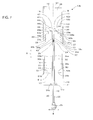
- Figure 7 is a plan view of an antenna 10E illustrated as another example.
- Figure 7 illustrates the axial direction with an arrow A, the width direction with an arrow B, and the central axial line S1 with a dashed-dotted line.
- the antenna 10E in Figure 7 is different from the antenna 10A in Figure 1 in that a plurality of resonance stepped portions 48 are formed at the first front end portion 29a of the first resonance area 27, a plurality of resonance stepped portions 49 are formed at the second front end portion 29b of the second resonance area 28, a plurality of attenuating stepped portions 50 are formed at the first rear end portion 34a of the first ground area 32, and a plurality of attenuating stepped portions 51 are formed at the second rear end portion 34b of the second ground area 33.
- the antenna 10E is comprised of the dielectric substrate 11 and the unbalanced power supply member 12, the resonance conductor 13 and the grounding conductor 14, and the radiation conductor 15.
- the dielectric substrate 11, the unbalanced power supply member 12, the resonance conductor 13, the grounding conductor 14 and the radiation conductor 15 are the same as those of the antenna 10A in Figure 1 .
- a separation dimension between the first and the second inner portions 30a and 30b of the first and the second resonance areas 27 and 28 and the central axial line S1, and a separation dimension between the first and the second inner portions 35a and 35b of the first and the second ground areas 32 and 33 are the same as those of the antenna 10A in Figure 1 .
- a total dimension of a length dimension in the axial direction of the resonance conductor 13 and a length dimension in the axial direction of the grounding conductor 14 is the same as that of the antenna 10A in Figure 1 .
- a plurality of resonance stepped portions 48 which dent stepwise backward in the axial direction toward outward in the width direction from the central axial line S1 (which distend stepwise forward in the axial direction toward the central axial line S1 from the first outer portion 31a of the area 27) are formed.
- the resonance stepped portions 48 include a first resonance stepped portion 48a which is located at a side of the central axial line S1 and which dents backward in the axial direction from the first front end portion 29a of the first resonance area 27, a second resonance stepped portion 48b which is located outward in a width direction of the first resonance stepped portion 48a and which dents backward in the axial direction from the first resonance stepped portion 48a, and a third resonance stepped portion 48c which is located outward in a width direction of the second resonance stepped portion 48b and which dents backward in the axial direction from the second resonance stepped portion 48b.
- the number of resonance stepped portions 48 is not limited to three, and four or more resonance stepped portions 48 may be formed.
- a plurality of resonance stepped portions 49 which dent stepwise backward in the axial direction toward outward in the width direction from the central axial line S1 (which distend stepwise forward in the axial direction toward the central axial line S from the second outer portion 31b of the area 28) are formed.
- the resonance stepped portions 49 include a first resonance stepped portion 49a which is located at a side of the central axial line S1 and which dents backward in the axial direction from the second front end portion 29b of the second resonance area 28, a second resonance stepped portion 49b which is located outward in a width direction of the first resonance stepped portion 49a and which dents backward in the axial direction from the first resonance stepped portion 49a, and a third resonance stepped portion 49c which is located outward in a width direction of the second resonance stepped portion 49b and which dents backward in the axial direction from the second resonance stepped portion 49b. It should be noted that the number of the resonance stepped portions 49 is not limited to three, and four or more resonance stepped portions 49 may be formed.
- a separation dimension in the axial direction between the first resonance stepped portions 48a and 49a of the first and the second resonance areas 27 and 18 and the first radiation stepped portions 42a and 44a of the second radiation area 38 is greater than a separation dimension in the axial direction between the first and the second front end portions 29a and 29b of the first and the second resonance areas 27 and 28 and the first and the second rear end portions 41 and 43 of the second radiation area 38, while a separation dimension in the axial direction between the second resonance stepped portions 48b and 49b and the second radiation stepped portions 42b and 44b is greater than a separation dimension in the axial direction between the first resonance stepped portions 48a and 49a and the first radiation stepped portions 42a and 44a.
- a separation dimension in the axial direction between the third resonance stepped portions 48c and 49c and the third radiation stepped portions 42c and 44c is greater than a separation dimension in the axial direction between the second resonance stepped portions 48b and 49b and the second radiation stepped portions 42b and 44b.
- a plurality of attenuating stepped portions 50 which dent stepwise forward in the axial direction toward outward in the width direction from the central axial line S1 (which distend stepwise backward in the axial direction toward the central axial line S1 from the first outer portion 36a of the area 32) are formed.
- the attenuating stepped portions 50 include a first attenuating stepped portion 50a which is located at a side of the central axial line S1 and which dents forward in the axial direction from the first rear end portion 34a of the first ground area 32, and a second attenuating stepped portion 50b which is located outward in a width direction of the first attenuating stepped portion 50a and which dents forward in the axial direction from the first attenuating stepped portion 50a. It should be noted that the number of the attenuating stepped portions 50 is not limited to two, and three or more attenuating stepped portions 50 may be formed.
- a plurality of attenuating stepped portions 51 which dent stepwise forward in the axial direction toward outward in the width direction from the central axial line S1 (which distend stepwise backward in the axial direction toward the central axial line S from the second outer portion 36b of the area 33) are formed.
- the attenuating stepped portions 51 include a first attenuating stepped portion 51a which is located at a side of the central axial line S1 and which dents forward in the axial direction from the second rear end portion 34b of the second ground area 33, and a second attenuating stepped portion 51b which is located outward in a width direction of the first attenuating stepped portion 51a and which dents forward in the axial direction from the first attenuating stepped portion 51 a. It should be noted that the number of attenuating stepped portions 51 is not limited to two, and three or more attenuating stepped portions 51 may be formed.
- a high frequency current of substantially the same direction flows between the first to the third radiation stepped portions 42a to 42c of the first rear end portion 41 of the second radiation area 38 and the first to the third resonance stepped portions 48a to 48c of the first front end portion 29a of the first resonance area 27, and the first to the third radiation stepped portions 42a to 42c and the first to the third resonance stepped portions 48a to 48c resonate at a plurality of points via the high frequency current of substantially the same direction, while a high frequency current of substantially the same direction flows between the first to the third radiation stepped portions 44a to 44c of the second rear end portion 43 of the second radiation area 38 and the first to the third resonance stepped portions 49a to 49c of the second front end portion 29b of the second resonance area 28, and the first to the third radiation stepped portions 44a to 44c and the first to the third resonance stepped portions 49a to 49c resonate at a plurality of points via the high frequency current of substantially the same direction.
- a high frequency current induced at the first and the second front end portions 29a and 29b of the first and the second resonance areas 27 and 28 and a high frequency current induced at the first and the second rear end portions 41 and 43 of the second radiation area 38 resonate, while a high frequency current induced at the first and the second resonance areas 27 and 28 (the first and the second inner portions 30a and 30b) and a high frequency current induced at the first radiation area 37 resonate.
- a radio is attenuated or blocked by the first and the second attenuating stepped portions 50a, 50b, 51a and 51b formed at the first and the second rear end portions 34a and 34b of the first and the second ground areas 32 and 33.
- the antenna 10E can obtain a plurality of resonance frequencies of different bands.
- the antenna 10E because a plurality of resonance frequencies of different bands can be obtained, and the obtained plurality of resonance frequencies are continuously adjacent to each other and partly overlap with each other, it is possible to drastically expand a use frequency band at the antenna 10E.
- the antenna 10E can achieve a VSWR of 2 or less, and can transmit or receive a radio wave in a full band among frequency bands (fractional bandwidths) which can be used, and the antenna 10E can be used in a wide band and can transmit or receive a radio wave of a wide band only with one antenna.
- the antenna 10E when a high frequency current flows at the first and the second rear end portions 34a and 34b of the first and the second ground areas 32 and 33, although the high frequency current flows through a chassis and a connection cable of a transceiver connected to the antenna 10E, which affects and changes a radiation pattern of a radio wave and a gain at the antenna 10E, because it is possible to attenuate or block the radio wave by the first and the second attenuating stepped portions 50a, 50b, 51a and 51b formed at the first and the second rear end portions 34a and 34b of the first and the second ground areas 32 and 33, the high frequency current does not flow through the chassis and the connection cable of the transceiver, so that it is possible to prevent change of the radiation pattern of the radio wave and the gain at the antenna 10E and secure a radiation pattern and a gain at the antenna 10E as designed.
- a length dimension in the axial direction of the grounding conductor 14 falls within a range between 10 and 15 cm, and the length dimension is set at length of approximately 1/4 (approximately ⁇ /4) of 700 MHz.
- the length dimension becomes length of approximately 1/4 wavelength of 700 MHz, it is possible to lower a lower limit frequency to 700 MHz while the size of the antenna 10E is kept small.
- Figure 8 is a plan view of an antenna 10F illustrated as another example
- Figure 9 is a plan view of an antenna 10G illustrated as another example.
- the antenna 10F in Figure 8 is different from the antennas in Figures 1 and 7 in that first to fourth slits 45a, 45b, 52a and 52b which penetrate the dielectric substrate 11 (print circuit board) are formed at the dielectric substrate 11, while the antenna 10G in Figure 9 is different from the antennas in Figures 1 and 7 in that a plurality of first to fourth through holes 46a, 46b, 53a and 53b which penetrate the dielectric substrate 11 (print circuit board) are formed at the dielectric substrate 11.
- a first slit 45a and a third slit 52a which penetrate the substrate 11 are formed.
- a second slit 45b and a fourth slit 52b which penetrate the substrate 11 are formed.
- the first slit 45a which is located near the radiation stepped portions 42 (the first to the third radiation stepped portions 42a to 42c), extends while tilting so as to gradually separate from the central axial line S1 toward forward in the axial direction from the first rear end portion 41.
- the second slit 45b which is located near the radiation stepped portions 44 (the first to the third radiation stepped portions 44a to 44c), extends while tilting so as to gradually separate from the central axial line S1 toward forward in the axial direction from the second rear end portion 43.
- the third slit 52a which is located near the resonance stepped portions 48 (the first to the third resonance stepped portions 48a to 48c), extends while tilting so as to gradually separate from the central axial line S1 toward backward in the axial direction from the first front end portion 29a. In other words, the third slit 52a extends along the first to the third resonance stepped portions 48a to 48c.
- the fourth slit 52b which is located near the resonance stepped portions 49 (the first to the third resonance stepped portions 49a to 49c), extends while tilting so as to gradually separate from the central axial line S1 toward backward in the axial direction from the second front end portion 29b. In other words, the fourth slit 52b extends along the first to the third resonance stepped portions 49a to 49c.
- a plurality of first through holes 46a and third through holes 53a which penetrate the substrate 11 are formed.
- a plurality of second through holes 46b and fourth through holes 53b which penetrate the substrate 11 are formed.
- the first through holes 36a which are located near the radiation stepped portions 42 (the first to the third radiation stepped portions 42a to 42c), are aligned while tilting so as to gradually separate from the central axial line S1 toward forward in the axial direction from the first rear end portion 41.
- the second through holes 46b which are located near the radiation stepped portions 44 (the first to the third radiation stepped portions 44a to 44c), are aligned while tilting so as to gradually separate from the central axial line S1 toward forward in the axial direction from the second rear end portion 43.
- the third through holes 53a which are located near the resonance stepped portions 48 (the first to the third resonance stepped portions 48a to 48c), are aligned while tilting so as to gradually separate from the central axial line S1 toward backward in the axial direction from the first front end portion 29a. In other words, the third through holes 53a are aligned along the first to the third resonance stepped portions 48a to 48c.
- the fourth through holes 53b which are located near the resonance stepped portions 49 (the first to the third resonance stepped portions 49a to 49c), are aligned while tilting so as to gradually separate from the central axial line S1 toward backward in the axial direction from the second front end portion 29b. In other words, the fourth through holes 53b are aligned along the first to the third resonance stepped portions 49a to 49c.
- the antennas 10F and 10G have the following advantageous effects in addition to the advantageous effects of the antennas 10A and 10E in Figures 1 and 7 .
- the first and the second slits 45a and 45b or the first and the second through holes 46a and 46b which are located near the first to the third radiation stepped portions 42a to 42c and 44a to 44c are formed at the dielectric substrate 11
- the third and the fourth slits 52a and 52b or the third and the fourth through holes 53a and 53b which are located near the first to the third resonance stepped portions 48a to 48c and 49a to 49c are formed at the dielectric substrate 11
- coupling capacitance of the substrate 11 which extends between the first and the second front end portions 29a and 29b of the first and the second resonance areas 27 and 28 and the first and the second rear end portions 41 and 43 of the second radiation area 38 can be reduced, so that it is possible to reduce a rate at which heat is dissipated instead of a radio wave being generated, and drastically
- the antennas 10F and 10G can increase radiation gains and can emit radio waves farther.
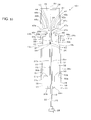
- Figure 10 is a plan view of an antenna 10H illustrated as another example.
- the antenna 10H in Figure 10 is different from the antennas in Figures 7 to 9 in that first and second void portions 47a and 47b are formed, and because other components of the antenna 10H are the same as those of the antennas 10E to 10G in Figures 7 to 9 , the same reference numerals as those of the antennas 10E to 10G in Figures 7 to 9 are assigned, and explanation of other components of the antenna 10H will be omitted by using explanation of the antennas 10E and 10G.
- the void portion 47a where the dielectric substrate 11 does not exist is formed between the first front end portion 29a of the first resonance area 27 and the first rear end portion 41 of the second radiation area 38.
- the void portion 47b where the dielectric substrate 121 does not exist is formed between the second front end portion 29b of the second resonance area 28 and the second rear end portion 43 of the second radiation area 38.
- the antenna 10H has the following advantageous effects in addition to the advantageous effects of the antennas 10A and 10E in Figures 1 and 7 .
- the antenna 10H because the first and the second void portions 47a and 47b where the dielectric substrate 11 does not exist are respectively formed between the first front end portion 29a of the first resonance area 27 and the first rear end portion 41 of the second radiation area 38 and between the second front end portion 29b of the second resonance area 28 and the second rear end portion 43 of the second radiation area 38, coupling capacitance between the first and the second front end portions 29a and 29b of the first and the second resonance areas 27 and 28 and the first and the second rear end portions 41 and 43 of the second radiation area 38 can be drastically reduced, so that it is possible to reduce a rate at which heat is dissipated instead of a radio wave being generated, and drastically improve tan ⁇ as an element of radio wave conversion efficiency at the antenna 10H.
- the antenna 10H can increase a radiation gain and can emit a radio
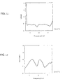
- Figure 11 illustrates correlation between a VSWR (voltage standing wave ratio) and a use frequency band of the antennas 10A to 10H
- Figure 12 illustrates gain characteristics of the antennas 10A to 10H
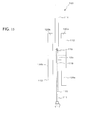
- Figures 13 and 14 illustrate radio field strength measured in a circumferential direction of three planes (an XY plane, a YZ plane and a ZX plane) of the antennas 10A to 10H.
- Figure 13 illustrates a measurement result of radio field strength of antenna characteristics of the XY plane in the circumferential direction (0° to 360°)
- Figure 14 illustrates a measurement result of radio field strength of antenna characteristics of the YZ plane or the ZX plane in the circumferential direction (0° to 360°).
- the antennas 10A to 10H has a VSWR (voltage standing wave ratio) of 2 or less in a use frequency of approximately 700 MHz to approximately 3.2 GHz, and it can be understood that the antennas 10A to 10H have a wide use frequency band while maintaining a low VSWR (voltage standing wave ratio). Further, as illustrated in Figure 12 , in the above-described use frequency band, the antennas 10A to 10H can obtain a gain of 2.5 dB or greater.
- radio field strength of the antenna characteristics of the XY plane in the circumferential direction (0° to 360°) are shaped in a substantially true circle
- radio field strength of the antenna characteristics of the YZ plane or the ZX plane in the circumferential direction (0° to 360°) are shaped in a butterfly, which indicates that the antennas 10A to 10H have favorable non-directional property.
Landscapes
- Details Of Aerials (AREA)
- Waveguide Aerials (AREA)
Abstract
Description
- The present invention relates to an antenna provided with an unbalanced power supply member, a resonance conductor, a grounding conductor and a radiation conductor.
- An
antenna 100 illustrated inFigure 15 is disclosed, theantenna 100 including an unbalanced power supply member having an outer conductor and an inner conductor as with a coaxial cable, and a plate like non-power supply element whose planar shape is molded in an H shape (see Patent Literature 1). As illustrated inFigure 15 , theantenna 100 ofPatent Literature 1 includes the unbalancedpower supply member 111, aresonance conductor 112, agrounding conductor 113 and apower supply element 114. Theresonance conductor 112 is formed with first andsecond resonance conductors power supply member 111 in parallel to apower supply unit 118. Thegrounding conductor 113 is formed with afixing portion 125 electrically connected to the unbalancedpower supply member 111, and first andsecond grounding conductors second resonance conductors non-power supply unit 119. Thepower supply element 114 has a predetermined area, extends forward in the axial direction, and is electrically connected to acentral conductor 115 of the unbalancedpower supply member 111 which constitutes thepower supply unit 118. - [Patent Literature 1]
Japanese Patent Laid-Open No.2012-195713 - The
antenna 100 disclosed inPatent Literature 1 can provide a wideband and high gain and can freely and finely adjusts a use frequency band. Specifically, in theantenna 100, a use frequency is approximately 2.0 GHz to approximately 4.0 GHz, and a VSWR (voltage standing wave ratio) is 2 or less. However, in theantenna 100 disclosed inPatent Literature 1, a lower limit frequency can neither be lowered to a lower frequency band (for example, 700 MHz) in a state where a wide band is maintained while a size of the antenna is kept small, nor the VSWR can be made 2 or less in a full band. - An object of the present invention is to provide an antenna which is capable of transmitting or receiving a radio wave in the full band among frequency bands (fractional bandwidth) which can be used, and the antenna which can be used in a wide band. Another object of the present invention is to provide an antenna which is capable of transmitting or receiving a radio wave in a wide frequency band, which can provide a high gain in a band between 700 MHz and 3.2 GHz, and which has a VSWR of 2 or less in a state where a size of the antenna is kept small.
- An antenna according to the present invention for solving the above-described problem includes a dielectric substrate having predetermined permittivity and having first and second regions sectioned by a central axial line dividing a width dimension, an unbalanced power supply member located on the central axial line and having a non-power supply unit and a power supply unit, the non-power supply unit extending in an axial direction and having predetermined length, and the power supply unit extending forward in the axial direction from the non-power supply unit, a resonance conductor molded into a plate shape having a predetermined area and fixed on one face of the dielectric substrate, a grounding conductor molded into a plate shape having a predetermined area, fixed on one face of the dielectric substrate and continuously coupled to the resonance conductor, and a radiation conductor molded into a plate shape having a predetermined area, fixed on one face of the dielectric substrate, and electrically connected to the power supply unit, and the resonance conductor has a connection area electrically connected to the unbalanced power supply member, a first resonance area coupled to the connection area, located in a first region of the dielectric substrate, and extending in the axial direction while separating outward in a width direction from the unbalanced power supply member by a predetermined dimension, and a second resonance area coupled to the connection area, located in a second region of the dielectric substrate, and extending in the axial direction while separating outward in the width direction from the unbalanced power supply member by a predetermined dimension, the grounding conductor has a first ground area located in the first region of the dielectric substrate, and extending backward in the axial direction from the first resonance area while separating outward in the width direction from the unbalanced power supply member by a predetermined dimension, and a second ground area located in the second region of the dielectric substrate, and extending backward in the axial direction from the second resonance area while separating outward in the width direction from the unbalanced power supply member by a predetermined dimension, the radiation conductor has a first radiation area located between the first and the second resonance areas and extending forward in the axial direction from the connection area of the resonance conductor, a rear end portion of the first radiation area being connected to the power supply unit, and a second radiation area extending forward in the axial direction from a front end portion of the first radiation area, a width dimension of the second radiation area being greater than a width dimension of the first radiation area, a plurality of radiation stepped portions denting stepwise forward in the axial direction toward outward in the width direction from the central axial line are formed at a first rear end portion of the second radiation area, facing the front end portion of the first resonance area, and a plurality of radiation stepped portions denting stepwise forward in the axial direction toward outward in the width direction from the central axial line are formed at a second rear end portion of the second radiation area, facing a front end portion of the second resonance area.
- As one example of the antenna according to the present invention, the radiation stepped portions formed at the first rear end portion of the second radiation area and the radiation stepped portions formed at the second rear end portion of the second radiation area have a first radiation stepped portion located at a side of the central axial line and denting forward in the axial direction from the first and second rear end portions, a second radiation stepped portion located outward in a width direction of the first radiation stepped portion and denting forward in the axial direction from the first radiation stepped portion, and a third radiation stepped portion located outward in a width direction of the second radiation stepped portion and tilting so as to gradually separate from the central axial line.
- As another one example of the antenna according to the present invention, a plurality of resonance stepped portions denting stepwise backward in the axial direction toward outward in the width direction from the central axial line are formed at the front end portion of the first resonance area, and a plurality of resonance stepped portions denting stepwise backward in the axial direction toward outward in the width direction from the central axial line are formed at the front end portion of the second resonance area.
- As another example of the antenna according to the present invention, the resonance stepped portions formed at the front end portion of the first resonance area and the resonance stepped portions formed at the front end portion of the second resonance area have a first resonance stepped portion located at a side of the central axial line and denting backward in the axial direction from the front end portions of the resonance areas, a second resonance stepped portion located outward in a width direction of the first resonance stepped portion and denting backward in the width direction from the first resonance stepped portion, and a third resonance stepped portion located outward in a width direction of the second resonance stepped portion and denting backward in the axial direction from the second resonance stepped portion.
- As another example of the antenna according to the present invention, a plurality of attenuating stepped portions denting stepwise forward in the axial direction toward outward in the width direction from the central axial line are formed at a rear end portion of the first ground area, and a plurality of attenuating stepped portions denting stepwise forward in the axial direction toward outward in the width direction from the central axial line are formed at the rear end portion of the second ground area.
- As another example of the antenna according to the present invention, the attenuating stepped portions formed at the rear end portion of the first ground area and the attenuating stepped portions formed at the rear end portion of the second ground area have a first attenuating stepped portion located at a side of the central axial line and denting forward in the axial direction from the rear end portions of the resonance areas and a second attenuating stepped portion located outward in a width direction of the first attenuating stepped portion and denting forward in the axial direction from the first attenuating stepped portion.
- As another example of the antenna according to the present invention, at the dielectric substrate extending between the front end portion of the first resonance area and the first rear end portion of the second radiation area, a first slit located near the radiation stepped portions and extending so as to gradually separate from the central axial line toward forward in the axial direction is formed, or a plurality of first through holes located near the radiation stepped portions and aligned so as to gradually separate from the central axial line toward forward in the axial direction are formed, and at the dielectric substrate extending between the front end portion of the second resonance area and the second rear end portion of the second radiation area, a second slit located near the radiation stepped portions and extending so as to gradually separate from the central axial line toward forward in the axial direction is formed, or a plurality of second through holes located near the radiation stepped portions and aligned so as to gradually separate from the central axial line toward forward in the axial direction are formed.
- As another example of the antenna according to the present invention, at the dielectric substrate extending between the front end portion of the first resonance area and the first rear end portion of the second radiation area, a third slit located near the resonance stepped portions and extending so as to gradually separate from the central axial line toward backward in the axial direction is formed, or a plurality of third through holes located near the resonance stepped portions and aligned so as to gradually separate from the central axial line toward backward in the axial direction are formed, and at the dielectric substrate extending between the front end potion of the second resonance area and the second rear end portion of the second radiation area, a fourth slit located near the resonance stepped portions and extending so as to gradually separate from the central axial line toward backward in the axial direction is formed, or a plurality of fourth through holes located near the resonance stepped portions and aligned so as to gradually separate from the central axial line toward backward in the axial direction are formed.
- As another example of the antenna according to the present invention, a first void portion where the dielectric substrate does not exist is formed between the front end portion of the first resonance area and the first rear end portion of the second radiation area, and a second void portion where the dielectric substrate does not exist is formed between the front end potion of the second resonance area and the second rear end portion of the second radiation area.
- As another example of the antenna according to the present invention, the first resonance area located in the first region and the second resonance area located in the second region are symmetric with respect to the central axial line, the first ground area located in the first region and the second ground area located in the second region are symmetric with respect to the central axial line, and the first and the second radiation areas located in the first region and the first and the second radiation areas located in the second region are symmetric with respect to the central axial line.
- As another example of the antenna according to the present invention, the unbalanced power supply member is formed with a first conductor extending in the axial direction, an insulator covering an outer periphery of the first conductor, and a second conductor covering an outer periphery of the insulator and extending in the axial direction, the non-power supply unit is formed with the first and the second conductors and the insulator, the power supply unit is formed with the first conductor, and the connection area of the resonance conductor is electrically connected to the second conductor.
- As another example of the antenna according to the present invention, a length dimension in the axial direction of the grounding conductor falls within a range between 10 and 15 cm, and is set at length of approximately 1/4 wavelength of 700 MHz.
- According to an antenna according to the present invention, because a plurality of radiation stepped portions which dent stepwise forward in the axial direction are formed at the first and the second rear end portions of the second radiation area, a high frequency current of substantially the same direction flows between the plurality of radiation stepped portions of the first and the second rear end portions of the second radiation area and the front end potions of first and second resonance areas of the resonance conductor, the radiation stepped portions of the second radiation area fixed at the dielectric substrate having predetermined permittivity and the front end portions of the first and the second resonance areas resonate at a plurality of points via the high frequency current of substantially the same direction, a high frequency current induced at the first radiation area fixed at the dielectric substrate and a high frequency current induced at the first and the second resonance areas resonate, while a high frequency current induced at the first and the second ground areas of the grounding conductor fixed at the dielectric substrate and a high frequency current induced at the non-power supply unit resonate, so that it is possible to obtain a plurality of resonance frequencies of different bands. The antenna can obtain a plurality of resonance frequencies of different bands, and because the obtained plurality of resonance frequencies are continuously adjacent to each other, and the resonance frequencies partly overlap with each other, it is possible to drastically expand a use frequency band at the antenna. The antenna can obtain a high gain whose VSWR (voltage standing wave ratio) is 2 or less, and can transmit or receive a radio wave in a full band among frequency bands (fractional bandwidths) which can be used, and the antenna can be used in a wide band, and can transmit or receive a radio wave of a wide band only with one antenna.
- In the antenna in which the first and the second rear end portions of the second radiation area have the first radiation stepped portion which is located at a side of the central axial line, the second radiation stepped portion which is located outward in a width direction of the first radiation stepped portion and a third radiation stepped portion which is located outward in a width direction of the second radiation stepped portion, a high frequency current of substantially the same direction flows between the first to the third radiation stepped portions of the first and the second rear end portions of the second radiation area and the front end portions of the first and the second resonance areas of the resonance conductor, the first to the third radiation stepped portions and the front end portions of the first and the second resonance areas resonate at a plurality of points via the high frequency current of substantially the same direction, a high frequency current induced at the first radiation area and a high frequency current induced at the first and the second resonance areas resonate, while a high frequency current induced at the first and the second ground areas and a high frequency current induced at the non-power supply unit resonate, so that it is possible to obtain a plurality of resonance frequencies of different bands. Because the resonance frequencies are continuously adjacent to each other and partly overlap with each other, the antenna can secure a wide use frequency band.
- In the antenna in which the plurality of resonance stepped portions are formed at the front end portion of the first resonance area, and the plurality of resonance stepped portions are formed at the front end portion of the second resonance area, a high frequency current of substantially the same direction flows between the plurality of radiation stepped portions of the second radiation area and the plurality of resonance stepped portions of the first and the second resonance areas, the radiation stepped portions and the resonance stepped portions resonate at a plurality of points via the high frequency current of substantially the same direction, a high frequency current induced at the first radiation area and a high frequency current induced at the first and the second resonance areas resonate, while a high frequency current induced at the first and the second ground areas and a high frequency current induced at the non-power supply unit resonate, so that it is possible to obtain a plurality of resonance frequencies of different bands. Because the resonance frequencies are continuously adjacent to each other and partly overlap with each other, the antenna can secure a wide use frequency band.
- In the antenna in which the resonance stepped portions of the first and the second resonance areas have the first resonance stepped portion located at a side of the central axial line, the second resonance stepped portion located outward in the width direction of the first resonance stepped portion, and the third resonance stepped portion located outward in the width direction of the second resonance stepped portion, a high frequency current of substantially the same direction flows between the first to the third radiation stepped portions of the first and the second rear end portions of the second radiation area and the first to the third resonance stepped portions of the front end portions of the first and the second resonance areas, the first to the third radiation stepped portions and the first to the third resonance stepped portions resonate at a plurality of points via the high frequency current of substantially the same direction, a high frequency current induced at the first radiation area and a high frequency current induced at the first and the second resonance areas resonate, while a high frequency current induced at the first and the second ground areas and a high frequency current induced at the non-power supply unit resonate, so that it is possible to obtain a plurality of resonance frequencies of different bands. Because the resonance frequencies are continuously adjacent to each other and partly overlap with each other, the antenna can secure a wide use frequency band.
- In the antenna in which the plurality of attenuating stepped portions are formed at the rear end portion of the first ground area and the plurality of attenuating stepped portions are formed at the rear end portion of the second ground area, when a high frequency current flows at the rear end portions of the first and the second ground areas, although the high frequency current flows through a chassis and a connection cable of a transceiver connected to the antenna, which affects and changes a radiation pattern of a radio wave and a gain at the antenna, because it is possible to attenuate or block the radio wave by the plurality of attenuating stepped portions formed at the rear end portions of the first and the second ground areas, the high frequency current does not flow through the chassis and the connection cable of the transceiver, so that it is possible to prevent change of the radiation pattern of the radio wave and the gain and secure a radiation pattern and a gain at the antenna as designed.
- In the antenna in which the attenuating stepped portions of the first and the second ground areas have the first attenuating stepped portion located at a side of the central axial line, and the second attenuating stepped portion located outward in the width direction of the first attenuating stepped portion, because it is possible to attenuate or block a radio wave by the first and the second attenuating stepped portions formed at the rear end portions of the first and the second ground areas, a high frequency current does not flow through the chassis and the connection cable of the transceiver, so that it is possible to prevent change of the radiation pattern of the radio wave and the gain at the antenna and secure a radiation pattern and a gain at the antenna as designed.
- In the antenna in which the first slit or the plurality of first through holes located near the radiation stepped portion is formed at the dielectric substrate which extends between the front end portion of the first resonance area and the first rear end portion of the second radiation area, and the second slit or the plurality of second through holes located near the radiation stepped portion is formed at the dielectric substrate which extends between the front end portion of the second resonance area and the second rear end portion of the second radiation area, because slits or through holes located near the radiation stepped portion are formed at the dielectric substrate, coupling capacitance of the dielectric substrate which extends between the front end portions of the first and the second resonance areas and the first and the second rear end portions of the second radiation area can be reduced, so that it is possible to reduce a rate at which heat is dissipated instead of a radio wave being generated, and drastically improve tanδ as an element of radio wave conversion efficiency at the antenna. As a result of slits or through holes being formed at the dielectric substrate near the radiation stepped portion, the antenna can increase a radiation gain and can emit a ratio wave farther.
- In the antenna in which the third slit or the plurality of third through holes located near the resonance stepped portion is formed at the dielectric substrate which extends between the front end potion of the first resonance area and the first rear end portion of the second radiation area, and the fourth slit or the plurality of fourth through holes located near the resonance stepped portion is formed at the dielectric substrate which extends between the front end portion of the second resonance area and the second rear end portion of the second radiation area, because slits or through holes located near the resonance stepped portion are formed at the dielectric substrate, coupling capacitance of the dielectric substrate which extends between the front end portions of the first and the second resonance areas and the first and the second rear end portions of the second radiation area can be reduced, so that it is possible to reduce a rate at which heat is dissipated instead of a radio wave being generated, and drastically improve tanδ as an element of radio wave conversion efficiency at the antenna. As a result of slits or through holes being formed at the dielectric substrate near the resonance stepped portion, the antenna can increase a radiation gain and can emit a radio wave farther.
- In the antenna in which the first void portion where the dielectric substrate does not exist is formed between the front end portion of the first resonance area and the first rear end portion of the second radiation area, and the second void portion where the dielectric substrate does not exist is formed between the front end portion of the second resonance area and the second rear end portion of the second radiation area, because the first and the second void portions where the dielectric substrate does not exist are respectively formed between the front end portion of the first resonance area and the first rear end portion of the second radiation area, and between the front end portion of the second resonance area and the second rear end portion of the second radiation area, coupling capacitance between the front end portions of the first and the second resonance areas and the first and the second rear end portions of the second radiation area can be drastically reduced, so that it is possible to reduce a rate at which heat is dissipated instead of a radio wave being generated, and drastically improve tanδ as an element of radio wave conversion efficiency at the antenna. As a result of the void portions being formed, the antenna can increase a radiation gain and can emit a radio wave farther.
- In the antenna in which the first resonance area located in the first region and the second resonance area located in the second region are symmetric with respect to the central axial line, the first ground area located in the first region and the second ground area located in the second region are symmetric with respect to the central axial line, and the first and the second radiation areas located in the first region and the first and the second radiation areas located in the second region are symmetric with respect to the central axial line, because the first and the second resonance areas, and the first and the second ground areas are made symmetric with respect to the central axial line, and the first and the second radiation areas located in the first region and the first and the second radiation areas located in the second region are made symmetric with respect to the central axial line, it is possible to prevent change of a radiation pattern of a radio wave which is caused by the first and the second resonance areas, the first and the second ground areas, and the first and the second radiation areas being asymmetric with respect to the central axial line, so that it is possible to secure a radiation pattern at the antenna as designed. As a result of the first and the second resonance areas, the first and the second ground areas, and the first and the second radiation areas being disposed so as to be symmetric with respect to the central axial line, the first and the second rear end portions of the second radiation area and the front end portions of the first and the second resonance areas of the resonance conductor resonate at a plurality of points at substantially the same coupling capacitance, the first radiation area and the first and the second resonance areas resonate, and the first and the second ground areas of the grounding conductor and the non-power supply unit resonate at substantially the same coupling capacitance, so that the antenna can obtain a plurality of resonance frequencies of different bands and secure a wide use frequency band.
- In the antenna in which the unbalanced power supply member is formed with the first conductor, the insulating body which covers the outer periphery of the first conductor, and the second conductor which covers the outer periphery of the insulating body and which extends in the axial direction, the non-power supply unit is formed with the first and the second conductors and the insulating body, and the connection area of the resonance conductor is electrically connected to the second conductor, the second radiation area and the first and the second resonance areas resonate at a plurality of points, and the first radiation area and the first and the second resonance areas resonate, so that the antenna can obtain a plurality of resonance frequencies of different bands and can secure a wide use frequency band. As a result of the insulating body being placed between the first conductor and the second conductor, the antenna can stably maintain impedance, can prevent a short circuit between the first conductor and the second conductor of the unbalanced power supply member, and can prevent breakage of a high frequency circuit of the transceiver due to a short circuit between the conductors.
- In the antenna in which the length dimension in the axial direction of the grounding conductor falls within a range between 10 and 15 cm and is set at length of approximately 1/4 wavelength of 700 MHz, because the length dimension in the axial direction of the grounding conductor falls within the above-described range, the length dimension becomes length of approximately 1/4 wavelength of 700 MHz, and a use frequency band at the antenna can be made to fall within a range of 700 MHz and 3.2 GHz, so that it is possible to lower a lower limit frequency to 700 MHz while the size of the antenna is kept small.
-
- [
Figure 1] Figure 1 is a plan view of an antenna illustrated as one example. - [
Figure 2] Figure 2 is a cross-sectional diagram cut along line 2-2 inFigure 1 . - [
Figure 3] Figure 3 is a cross-sectional diagram cut along line 3-3 inFigure 1 . - [
Figure 4] Figure 4 is a plan view of an antenna illustrated as another example. - [
Figure 5] Figure 5 is a plan view of an antenna illustrated as another example. - [
Figure 6] Figure 6 is a plan view of an antenna illustrated as another example. - [
Figure 7] Figure 7 is a plan view of an antenna illustrated as another example. - [
Figure 8] Figure 8 is a plan view of an antenna illustrated as another example. - [
Figure 9] Figure 9 is a plan view of an antenna illustrated as another example. - [
Figure 10] Figure 10 is a plan view of an antenna illustrated as another example. - [
Figure 11] Figure 11 is a diagram illustrating correlation between a VSWR (voltage standing wave ratio) and a use frequency band. - [
Figure 12] Figure 12 is a diagram illustrating gain characteristics of the antenna. - [
Figure 13] Figure 13 is a diagram illustrating radio field strength measured in a circumferential direction of three planes of the antenna. - [
Figure 14] Figure 14 is a diagram illustrating radio field strength measured in a circumferential direction of three planes of the antenna. - [
Figure 15] Figure 15 is a plane view of an antenna according to a conventional technique. - Details of an embodiment of an antenna according to the present invention will be described below with reference to the accompanying drawings such as
Figure 1 which is a plan view of anantenna 10A illustrated as one example. It should be noted thatFigure 2 is a cross-sectional diagram cut along line 2-2 inFigure 1 , andFigure 3 is a cross-sectional diagram cut along line 3-3 inFigure 1. Figure 1 illustrates an axial direction with an arrow A, a width direction with an arrow B, forward in the axial direction i with an arrow A1, and backward in the axial direction with an arrow A2.Figure 1 illustrates a central axial line S1 with a dashed-dotted line. - The
antenna 10A is comprised of a dielectric substrate 11 (print circuit board) having predetermined permittivity and an unbalanced power supply member 12 (a coaxial cable or a semi-rigid cable), aresonance conductor 13 and agrounding conductor 14, and aradiation conductor 15. Thedielectric substrate 11 is formed with glass epoxy having predetermined permittivity. Thedielectric substrate 11 can be also formed with a thermoplastic synthetic resin or a thermosetting synthetic resin having predetermined permittivity, or a ceramic substrate, other than glass epoxy - The
dielectric substrate 11 which has a plate shape having predetermined thickness, is molded so that the planar shape of thedielectric substrate 11 is a rectangle which is elongated in the axial direction. Thedielectric substrate 11 has an upper face 16 (one face) and a lower face 17 (the other face), and has afirst region 18 and asecond region 19 sectioned by the central axial line S1 which divides a width direction of thedielectric substrate 11. Thedielectric substrate 11 serves as a capacitor in which electric charge is accumulated at theantenna 10A. A length dimension in the axial direction, a length dimension in the width direction, and a thickness dimension between theupper face 16 and thelower face 17 of thedielectric substrate 11 are not particularly limited and are freely designed, so that a frequency bandwidth can be freely adjusted. - The unbalanced
power supply member 12 is located on the central axial line S1 on theupper face 16 of thedielectric substrate 11, has predetermined length and extends in the axial direction. As illustrated inFigures 1 and2 , the unbalancedpower supply member 12 is comprised of a rod-like elongated first conductor 20 (central metal conductor), an insulatingbody 21 which has a circular cross section and which covers an outer periphery of thefirst conductor 20, and a second conductor 22 (external metal conductor) which has a cylindrical cross section and which covers an outer periphery of the insulatingbody 21. At the unbalancedpower supply member 12, an outer periphery of thefirst conductor 20 is fixedly attached to an inner periphery of the insulatingbody 21, and an outer periphery of the insulatingbody 21 is fixedly attached to an inner periphery of thesecond conductor 22. The unbalancedpower supply member 12 has anon-power supply unit 23 which is set to have predetermined length (approximately λ/4) and which vertically extends in the axial direction, and apower supply unit 24 which extends forward in the axial direction from thenon-power supply unit 23. Aconnector 25 is attached to a rear end of the unbalancedpower supply member 12. - The
non-power supply unit 23 is comprised of thefirst conductor 20, the insulatingbody 21 and thesecond conductor 22. Thepower supply unit 24 is comprised of thefirst conductor 20. A conductive metal such as gold, nickel, copper and silver can be used as thefirst conductor 20 and thesecond conductor 22, and thermoplastic synthetic resin (particularly, polytetrafluoroethylene having plastic permittivity) which becomes a material for fixing impedance of the unbalancedpower supply member 12 can be used as the insulatingbody 21. - The
resonance conductor 13 is formed with a conductive metal (such as gold, nickel, copper and silver) and is molded in a plate shape having a predetermined area. Theresonance conductor 13 is fixed on the upper face of thedielectric substrate 11. Theresonance conductor 13 has aconnection area 26 electrically connected to the unbalancedpower supply member 12, afirst resonance area 27 located in thefirst region 18 of thedielectric substrate 11, and asecond resonance area 28 located in thesecond region 19 of thedielectric substrate 11. - The
connection area 26 extends in a width direction across the central axial line S1. A periphery of thesecond conductor 22 of the unbalancedpower supply member 12 abuts on theconnection area 26, and thesecond conductor 20 is electrically connected (fixed) to theconnection area 26 through molding (such as soldering) (fixing means). Thefirst resonance area 27 is coupled to theconnection area 26, and extends in the axial direction while separating outward in the width direction from the central axial line S1 (first radiation area of a radiation conductor which will be described later) by a predetermined dimension. Thesecond resonance area 28 is coupled to theconnection area 26, and extends in the axial direction while separating outward in the width direction from the central axial line S1 (first radiation area of the radiation conductor) by a predetermined dimension. Theconnection area 26 and the first and thesecond resonance areas upper face 16 of thedielectric substrate 11. Thefirst resonance area 27 and thesecond resonance area 28 are shaped in a rectangle which has a predetermined width dimension and which is elongated in the axial direction, and have planar shapes of the same shape and the same size, which are symmetric with respect to the central axial line S1. - The
first resonance area 27 has a firstfront end portion 29a extending in the width direction, and a firstinner portion 30a and a firstouter portion 31 a extending in the axial direction, and thesecond resonance area 28 has a secondfront end portion 29b extending in the width direction, and a secondinner portion 30b and a secondouter portion 31b extending in the axial direction. In the first and thesecond resonance areas front end portions inner portions outer portions inner portions first radiation area 37 of the radiation conductor 15), and theinner portions - The grounding
conductor 14 which is formed with a conductive metal (such as gold, nickel, copper and silver), is molded in a plate shape having a predetermined area, and continuously coupled to the resonance conductor 13 (integrally formed with the resonance conductor 13). The groundingconductor 14 is fixed on theupper face 16 of thedielectric substrate 11. The groundingconductor 14 has afirst ground area 32 located in thefirst region 18 of thedielectric substrate 11, and asecond ground area 33 located in thesecond region 19 of thedielectric substrate 11. - The
first ground area 32 is coupled to thefirst resonance area 27 and extends backward in the axial direction from thefirst resonance area 27 while separating outward in the width direction from the central axial line S1 (unbalanced power supply member 12) by a predetermined dimension. Thesecond ground area 33 is coupled to thesecond resonance area 28 and extends backward in the axial direction from thesecond resonance area 28 while separating outward in the width direction from the central axial line S1 (unbalanced power supply member 12) by a predetermined dimension. Thefirst ground area 32 and thesecond ground area 33 are fixed on theupper face 16 of thedielectric substrate 11. Thefirst ground area 32 and thesecond ground area 33 are shaped in a rectangle which has a predetermined width dimension and which is elongated in the axial direction, and have planar shapes of the same shape and the same size, which are symmetric with respect to the central axial line S1. - The
first ground area 32 has a firstrear end portion 34a extending in the width direction, and a firstinner portion 35a and a firstouter portion 36a extending in the axial direction, and thesecond ground area 33 has a secondrear end portion 34b extending in the width direction, and a secondinner portion 35b and a secondouter portion 36b extending in the axial direction. In the first and thesecond ground areas rear end portions inner portions outer portions inner portions inner portions - The
radiation conductor 15 which is formed with a conductive metal (such as gold, nickel, copper and silver), is molded in a plate shape having a predetermined area, and fixed on theupper face 16 of thedielectric substrate 11. Theradiation conductor 15 has afirst radiation area 37 which is located between the first and thesecond resonance areas connection area 26, and asecond radiation area 38 which extends forward in the axial direction from afront end portion 39 of thefirst radiation area 37. The first and thesecond radiation areas - The
first radiation area 37 is located between the first and thesecond resonance areas resonance conductor 13. Thefirst radiation area 37 has a rectangular shape which has a predetermined width dimension and which is elongated in the axial direction, and is fixed on theupper face 16 of thedielectric substrate 11. In thefirst radiation area 37, thearea 37 located in thefirst region 18 of thedielectric substrate 11 and thearea 37 located in thesecond region 19 of thedielectric substrate 11 are symmetric with respect to the central axial line S1. Therear end portion 40 of thefirst radiation area 37 is electrically connected to thepower supply unit 24 of the unbalancedpower supply member 12. - The
second radiation area 38 separates forward in the axial direction from the first and the secondfront end portions second resonance areas upper face 16 of thedielectric substrate 11. Thesecond radiation area 38 has a larger width dimension than a width dimension of thefirst radiation area 37. In thesecond radiation area 38, thearea 38 located in thefirst region 18 of thedielectric substrate 11 and thearea 38 located in thesecond region 19 of thedielectric substrate 11 are symmetric with respect to the central axial line S1. - At the first
rear end portion 41 of thesecond radiation area 38, facing the firstfront end portion 29a of thefirst resonance area 27, a plurality of radiation steppedportions 42 which dent stepwise forward in the axial direction toward outward of the width direction from the central axial line S1 (which distend stepwise backward in the axial direction toward the central axial line S1 from both side portions of the area 38) are formed. The radiation steppedportions 42 include a first radiation steppedportion 42a which is located at a side of the central axial line S1 and which dents forward in the axial direction from the firstrear end portion 41, a second radiation steppedportion 42b which is located outward in a width direction of the first radiation steppedportion 42a and which dents forward in the axial direction from the first radiation steppedportion 42a, and a third radiation steppedportion 42c which is located outward in a width direction of the second radiation steppedportion 42b and which tilts so as to gradually separate from the central axial line S1. It should be noted that the number of radiation steppedportions 42 is not limited to three, and four or more steppedradiation portions 42 may be formed. - At the second
rear end portion 43 of thesecond radiation area 38, facing the secondfront end portion 29b of thesecond resonance area 28, a plurality of radiation steppedportions 44 which dent stepwise forward in the axial direction toward outward in the width direction from the central axial line S1 (which distend stepwise backward in the axial direction toward the central axial line S1 from both side portions of the area 38) are formed. The radiation steppedportions 44 include a first radiation steppedportion 44a which is located at a side of the central axial line S1 and which dents forward in the axial direction from the secondrear end portion 43, a second radiation steppedportion 44b which is located outward in a width direction of the first radiation steppedportion 44a and which dents forward in the axial direction from the first radiation steppedportion 44a, and a third radiation steppedportion 44c which is located outward in a width direction of the second radiation steppedportion 44b and which tilts so as to gradually separate from the central axial line S1. It should be noted that the number of the radiation steppedportions 44 is not limited to three, and four or more radiation steppedportions 44 may be formed. - A separation dimension in the axial direction between the first and the second
front end portions second resonance areas portions front end portions second resonance areas rear end portions second radiation area 38, and a separation dimension in the axial direction between the first and the secondfront end portions portions front end portions portions front end portions portions front end portions portions - At the
antenna 10A, thedielectric substrate 11 having predetermined permittivity serves as a dielectric body, a high frequency current of substantially the same direction flows between the first to the third radiation steppedportions 42a to 42c of the firstrear end portion 41 of thesecond radiation area 38 and the firstfront end portion 29a of thefirst resonance area 27, and the first to the third radiation steppedportions 42a to 42c and the firstfront end portion 29a resonate at a plurality of points via the high frequency current of substantially the same direction, while a high frequency current of substantially the same direction flows between the first to the third radiation steppedportions 44a to 44c of the secondrear end portion 43 of thesecond radiation area 38 and the secondfront end portion 29b of thesecond resonance area 28, and the first to the third radiation steppedportions 44a to 44c and the secondfront end portion 29b resonate at a plurality of points via the high frequency current of substantially the same direction. - Further, at the
antenna 10A, a high frequency current induced at the first and the secondfront end portions second resonance areas rear end portions second radiation area 38 resonate, while a high frequency current induced at thesecond resonance areas 27 and 28 (first and the secondinner portions first radiation area 37 resonate. - Because the
second radiation area 38 and the first and thesecond resonance areas second resonance areas first radiation area 37 resonate, theantenna 10A can obtain a plurality of resonance frequencies of different bands. Because theantenna 10A can obtain a plurality of resonance frequencies of different bands, and the obtained plurality of resonance frequencies are continuously adjacent to each other and partly overlap with each other, it is possible to drastically expand a use frequency band at theantenna 10A. Theantenna 10A can achieve a VSWR of 2 or less, and can transmit or receive a radio wave in a full band among frequency bands (fractional bandwidths) which can be used, and the antenna can be used in a wide band, and can transmit or receive a radio wave of a wide band only with one antenna. - At the
antenna 10A, a separation dimension between the first and the secondinner portions second resonance areas inner portions second ground areas antenna 10A can use the widest frequency band, and the frequency band of theantenna 10A cannot be expanded wider. By changing these separation dimensions within the above-described ranges, it is possible to adjust a use frequency band to be wider or narrower, so that it is possible to stabilize a resonance band. - The
antenna 10A can achieve optimal resonance efficiency of a radio wave by these separation dimensions being set to fall within the above-described ranges, so that it is possible to make thesecond radiation area 38 and the first and thesecond resonance areas second resonance areas first radiation area 37 resonate efficiently. - At the
antenna 10A, a length dimension in the axial direction of the groundingconductor 14 falls within a range of 10 and 15 cm, and the length dimension is set to be length of approximately 1/4 wavelength (approximately λ/4) of 700 MHz. By setting the length dimension to fall within the above-described range, the length dimension becomes length of approximately 1/4 wavelength of 700 MHz, so that it is possible to lower a lower limit frequency to 700 MHz while the size of theantenna 10A is kept small. -
Figure 4 is a plan view of anantenna 10B illustrated as another example, andFigure 5 is a plan view of anantenna 10C illustrated as another example. Theantenna 10B inFigure 4 is different from theantenna 10A inFigure 1 in that first andsecond slits dielectric substrate 11, and theantenna 10C inFigure 5 is different from theantenna 10A inFigure 1 in that a plurality of first and second throughholes dielectric substrate 11. Because other components of theantennas antenna 10A inFigure 1 , the same reference numerals as those ofantenna 10A inFigure 1 are assigned, and explanation of other components of theantennas antenna 10A. - As with the
antenna 10A inFigure 1 , each of theantennas dielectric substrate 11 and the unbalancedpower supply member 12, theresonance conductor 13 and thegrounding conductor 14, and theradiation conductor 15. Thedielectric substrate 11, the unbalancedpower supply member 12, theresonance conductor 13, the groundingconductor 14 and theradiation conductor 15 are the same as those of theantenna 10A inFigure 1 . Further, a separation dimension between the first and the secondinner portions second resonance areas inner portions second ground areas antenna 10A inFigure 1 . A total dimension of a length dimension in the axial direction of theresonance conductor 13 and a length dimension in the axial direction of the groundingconductor 14 are the same as that of theantenna 10A inFigure 1 . - At the
dielectric substrate 11 which extends between the firstfront end portion 29a of thefirst resonance area 27 and the firstrear end portion 41 of thesecond radiation area 38 of theantenna 10B, afirst slit 45a which penetrates thesubstrate 11 is formed. At thedielectric substrate 11 which extends between the secondfront end portion 29b of thesecond resonance area 28 and the secondrear end portion 43 of thesecond radiation area 38 of theantenna 10B, asecond slit 45b which penetrates thesubstrate 11 is formed. - The
first slit 45a which is located near the radiation stepped portions 42 (the first to the third radiation steppedportions 42a to 42c), extends while tilting so as to gradually separate from the central axial line S1 toward forward in the axial direction from the firstrear end portion 41. In other words, thefirst slit 45a extends along the first to the third radiation steppedportions 42a to 42c. Thesecond slit 45b which is located near the radiation stepped portions 44 (the first to the third radiation steppedportions 44a to 44c), extends while tilting so as to gradually separate from the central axial line S1 toward forward in the axial direction from the secondrear end portion 43. In other words, thesecond slit 45b extends along the first to the third radiation steppedportions 44a to 44c. - At the
dielectric substrate 11 which extends between the firstfront end portion 29a of thefirst resonance area 27 and the firstrear end portion 41 of thesecond radiation area 38 of theantenna 10C, a plurality of first throughholes 46a which penetrate thesubstrate 11 are formed. At thedielectric substrate 11 which extends between the secondfront end portion 29b of thesecond resonance area 28 and the secondrear end portion 43 of thesecond radiation area 38 of theantenna 10C, a plurality of second throughholes 46b which penetrate thesubstrate 11 are formed. - The first through
holes 46a which are located near the radiation stepped portions 42 (the first to the third radiation steppedportions 42a to 42c), are aligned while tilting so as to gradually separated from the central axial line S1 toward forward in the axial direction from the firstrear end portion 41. In other words, the first throughholes 46a are aligned along the first to the third radiation steppedportions 42a to 42c. The second throughholes 46b which are located near the radiation stepped portions 44 (the first to the third radiation steppedportions 44a to 44c), are aligned while tilting so as to gradually separate from the central axial line S1 toward forward in the axial direction from the secondrear end portion 43. In other words, the second throughholes 46b are aligned along the first to the third radiation steppedportions 44a to 44c. - These
antennas antenna 10A inFigure 1 . In theantennas second slits holes portions 42a to 42c and 44a to 44c, are formed on thedielectric substrate 11, coupling capacitance of thesubstrate 11 which extends between the first and the secondfront end portions second resonance areas rear end portions second radiation area 38 can be reduced, so that it is possible to drastically improve tanδ as an element of radio wave conversion efficiency at theantennas slits holes dielectric substrate 11 near the radiation steppedportions 42a to 42c and 44a to 44c, theantennas -
Figure 6 is a plan view of an antenna 10d illustrated as another example. Theantenna 10D inFigure 6 is different from the antennas inFigures 1 ,4 and5 in that first andsecond void portions antenna 10D are the same as those of theantennas 10A to 10C inFigures 1 ,4 and5 , the same reference numerals as those of theantennas 10A to 10C inFigures 1 ,4 and5 are assigned, and explanation of other components of theantenna 10D will be omitted by using explanation of theantennas 10A to 10C. - A
void portion 47a where thedielectric substrate 11 does not exist is formed between the firstfront end portion 29a of thefirst resonance area 27 and the firstrear end potion 41 of thesecond radiation area 38. Avoid portion 47b where thedielectric substrate 11 does not exist is formed between the secondfront end portion 29b of thesecond resonance area 28 and the secondrear end portion 43 of thesecond radiation area 38. While thesevoid portions void portions dielectric substrate 11 does not exist is formed between the firstfront end portion 29a and the firstrear end portion 41, and between the secondfront end portion 29b and the secondrear end portion 43. - The
antenna 10D has the following advantageous effects in addition to the advantageous effects of theantenna 10A inFigure 1 . In theantenna 10D, because the first and thesecond void portions dielectric substrate 11 does not exist are formed between the firstfront end portion 29a of thefirst resonance area 27 and the firstrear end portion 41 of thesecond radiation area 38 and between the secondfront end portion 29b of thesecond resonance area 28 and the secondrear end portion 43 of thesecond radiation area 38, coupling capacitance between the first and the secondfront end portions second resonance areas rear end portions second radiation area 38 can be drastically reduced, so that it is possible to reduce a rate at which heat is dissipated instead of a radio wave being generated, and it is possible to drastically improve tanδ as an element of radio wave conversion efficiency at theantenna 10D. As a result of thevoid portions antenna 10D can increase a radiation gain and can emit a radio wave farther. -
Figure 7 is a plan view of anantenna 10E illustrated as another example.Figure 7 illustrates the axial direction with an arrow A, the width direction with an arrow B, and the central axial line S1 with a dashed-dotted line. Theantenna 10E inFigure 7 is different from theantenna 10A inFigure 1 in that a plurality of resonance steppedportions 48 are formed at the firstfront end portion 29a of thefirst resonance area 27, a plurality of resonance steppedportions 49 are formed at the secondfront end portion 29b of thesecond resonance area 28, a plurality of attenuating steppedportions 50 are formed at the firstrear end portion 34a of thefirst ground area 32, and a plurality of attenuating steppedportions 51 are formed at the secondrear end portion 34b of thesecond ground area 33. Because other components of theantenna 10E are the same as those of theantenna 10A inFigure 1 , the same reference numerals as those of theantenna 10A inFigure 1 are assigned, and explanation of other components of theantenna 10E will be omitted by using explanation of theantenna 10A. - As with the
antenna 10A inFigure 1 , theantenna 10E is comprised of thedielectric substrate 11 and the unbalancedpower supply member 12, theresonance conductor 13 and thegrounding conductor 14, and theradiation conductor 15. Thedielectric substrate 11, the unbalancedpower supply member 12, theresonance conductor 13, the groundingconductor 14 and theradiation conductor 15 are the same as those of theantenna 10A inFigure 1 . Further, a separation dimension between the first and the secondinner portions second resonance areas inner portions second ground areas antenna 10A inFigure 1 . A total dimension of a length dimension in the axial direction of theresonance conductor 13 and a length dimension in the axial direction of the groundingconductor 14 is the same as that of theantenna 10A inFigure 1 . - At the first
front end portion 29a of thefirst resonance area 27, a plurality of resonance steppedportions 48 which dent stepwise backward in the axial direction toward outward in the width direction from the central axial line S1 (which distend stepwise forward in the axial direction toward the central axial line S1 from the firstouter portion 31a of the area 27) are formed. The resonance steppedportions 48 include a first resonance steppedportion 48a which is located at a side of the central axial line S1 and which dents backward in the axial direction from the firstfront end portion 29a of thefirst resonance area 27, a second resonance steppedportion 48b which is located outward in a width direction of the first resonance steppedportion 48a and which dents backward in the axial direction from the first resonance steppedportion 48a, and a third resonance steppedportion 48c which is located outward in a width direction of the second resonance steppedportion 48b and which dents backward in the axial direction from the second resonance steppedportion 48b. It should be noted that the number of resonance steppedportions 48 is not limited to three, and four or more resonance steppedportions 48 may be formed. - At the second
front end portion 29b of thesecond resonance area 28, a plurality of resonance steppedportions 49 which dent stepwise backward in the axial direction toward outward in the width direction from the central axial line S1 (which distend stepwise forward in the axial direction toward the central axial line S from the secondouter portion 31b of the area 28) are formed. The resonance steppedportions 49 include a first resonance steppedportion 49a which is located at a side of the central axial line S1 and which dents backward in the axial direction from the secondfront end portion 29b of thesecond resonance area 28, a second resonance steppedportion 49b which is located outward in a width direction of the first resonance steppedportion 49a and which dents backward in the axial direction from the first resonance steppedportion 49a, and a third resonance steppedportion 49c which is located outward in a width direction of the second resonance steppedportion 49b and which dents backward in the axial direction from the second resonance steppedportion 49b. It should be noted that the number of the resonance steppedportions 49 is not limited to three, and four or more resonance steppedportions 49 may be formed. - A separation dimension in the axial direction between the first resonance stepped
portions second resonance areas portions second radiation area 38 is greater than a separation dimension in the axial direction between the first and the secondfront end portions second resonance areas rear end portions second radiation area 38, while a separation dimension in the axial direction between the second resonance steppedportions portions portions portions portions portions portions portions - At the first
rear end portion 34a of the first ground area, a plurality of attenuating steppedportions 50 which dent stepwise forward in the axial direction toward outward in the width direction from the central axial line S1 (which distend stepwise backward in the axial direction toward the central axial line S1 from the firstouter portion 36a of the area 32) are formed. The attenuating steppedportions 50 include a first attenuating steppedportion 50a which is located at a side of the central axial line S1 and which dents forward in the axial direction from the firstrear end portion 34a of thefirst ground area 32, and a second attenuating steppedportion 50b which is located outward in a width direction of the first attenuating steppedportion 50a and which dents forward in the axial direction from the first attenuating steppedportion 50a. It should be noted that the number of the attenuating steppedportions 50 is not limited to two, and three or more attenuating steppedportions 50 may be formed. - At the second
rear end portion 34b of thesecond ground area 33, a plurality of attenuating steppedportions 51 which dent stepwise forward in the axial direction toward outward in the width direction from the central axial line S1 (which distend stepwise backward in the axial direction toward the central axial line S from the secondouter portion 36b of the area 33) are formed. The attenuating steppedportions 51 include a first attenuating steppedportion 51a which is located at a side of the central axial line S1 and which dents forward in the axial direction from the secondrear end portion 34b of thesecond ground area 33, and a second attenuating steppedportion 51b which is located outward in a width direction of the first attenuating steppedportion 51a and which dents forward in the axial direction from the first attenuating steppedportion 51 a. It should be noted that the number of attenuating steppedportions 51 is not limited to two, and three or more attenuating steppedportions 51 may be formed. - At the
antenna 10E, a high frequency current of substantially the same direction flows between the first to the third radiation steppedportions 42a to 42c of the firstrear end portion 41 of thesecond radiation area 38 and the first to the third resonance steppedportions 48a to 48c of the firstfront end portion 29a of thefirst resonance area 27, and the first to the third radiation steppedportions 42a to 42c and the first to the third resonance steppedportions 48a to 48c resonate at a plurality of points via the high frequency current of substantially the same direction, while a high frequency current of substantially the same direction flows between the first to the third radiation steppedportions 44a to 44c of the secondrear end portion 43 of thesecond radiation area 38 and the first to the third resonance steppedportions 49a to 49c of the secondfront end portion 29b of thesecond resonance area 28, and the first to the third radiation steppedportions 44a to 44c and the first to the third resonance steppedportions 49a to 49c resonate at a plurality of points via the high frequency current of substantially the same direction. - Further, at the
antenna 10E, a high frequency current induced at the first and the secondfront end portions second resonance areas rear end portions second radiation area 38 resonate, while a high frequency current induced at the first and thesecond resonance areas 27 and 28 (the first and the secondinner portions first radiation area 37 resonate. At theantenna 10E, a radio is attenuated or blocked by the first and the second attenuating steppedportions rear end portions second ground areas - Because the
second radiation area 38 and the first and thesecond resonance areas second resonance areas first radiation area 37 resonate, theantenna 10E can obtain a plurality of resonance frequencies of different bands. At theantenna 10E, because a plurality of resonance frequencies of different bands can be obtained, and the obtained plurality of resonance frequencies are continuously adjacent to each other and partly overlap with each other, it is possible to drastically expand a use frequency band at theantenna 10E. Theantenna 10E can achieve a VSWR of 2 or less, and can transmit or receive a radio wave in a full band among frequency bands (fractional bandwidths) which can be used, and theantenna 10E can be used in a wide band and can transmit or receive a radio wave of a wide band only with one antenna. - At the
antenna 10E, when a high frequency current flows at the first and the secondrear end portions second ground areas antenna 10E, which affects and changes a radiation pattern of a radio wave and a gain at theantenna 10E, because it is possible to attenuate or block the radio wave by the first and the second attenuating steppedportions rear end portions second ground areas antenna 10E and secure a radiation pattern and a gain at theantenna 10E as designed. - At the
antenna 10E, by setting a separation dimension between the first and the secondinner portions second resonance areas inner portions second ground areas second radiation area 38 and the first and thesecond resonance areas second resonance areas first radiation area 37 efficiently resonate, and make thenon-power supply unit 22 and the first and thesecond ground areas - At the
antenna 10E, a length dimension in the axial direction of the groundingconductor 14 falls within a range between 10 and 15 cm, and the length dimension is set at length of approximately 1/4 (approximately λ/4) of 700 MHz. By setting the length dimension within the above-described range, because the length dimension becomes length of approximately 1/4 wavelength of 700 MHz, it is possible to lower a lower limit frequency to 700 MHz while the size of theantenna 10E is kept small. -
Figure 8 is a plan view of anantenna 10F illustrated as another example, andFigure 9 is a plan view of anantenna 10G illustrated as another example. Theantenna 10F inFigure 8 is different from the antennas inFigures 1 and7 in that first tofourth slits dielectric substrate 11, while theantenna 10G inFigure 9 is different from the antennas inFigures 1 and7 in that a plurality of first to fourth throughholes dielectric substrate 11. Because other components of theantennas antennas Figures 1 and7 , the same reference numerals as those of theantennas antennas antennas - At the
dielectric substrate 11 which extends between the firstfront end portion 29a of thefirst resonance area 27 and the firstrear end portion 41 of thesecond radiation area 38 of theantenna 10F, afirst slit 45a and athird slit 52a which penetrate thesubstrate 11 are formed. At thedielectric substrate 11 which extends between the secondfront end portion 29b of thesecond resonance area 28 and the secondrear end portion 43 of thesecond radiation area 38 of theantenna 10F, asecond slit 45b and afourth slit 52b which penetrate thesubstrate 11 are formed. - The
first slit 45a which is located near the radiation stepped portions 42 (the first to the third radiation steppedportions 42a to 42c), extends while tilting so as to gradually separate from the central axial line S1 toward forward in the axial direction from the firstrear end portion 41. Thesecond slit 45b which is located near the radiation stepped portions 44 (the first to the third radiation steppedportions 44a to 44c), extends while tilting so as to gradually separate from the central axial line S1 toward forward in the axial direction from the secondrear end portion 43. - The
third slit 52a which is located near the resonance stepped portions 48 (the first to the third resonance steppedportions 48a to 48c), extends while tilting so as to gradually separate from the central axial line S1 toward backward in the axial direction from the firstfront end portion 29a. In other words, thethird slit 52a extends along the first to the third resonance steppedportions 48a to 48c. Thefourth slit 52b which is located near the resonance stepped portions 49 (the first to the third resonance steppedportions 49a to 49c), extends while tilting so as to gradually separate from the central axial line S1 toward backward in the axial direction from the secondfront end portion 29b. In other words, thefourth slit 52b extends along the first to the third resonance steppedportions 49a to 49c. - At the
dielectric substrate 11 which extends between the firstfront end portion 29a of thefirst resonance area 27 and the firstrear end portion 41 of thesecond radiation area 38 of theantenna 10G, a plurality of first throughholes 46a and third throughholes 53a which penetrate thesubstrate 11 are formed. At thedielectric substrate 11 which extends between the secondfront end portion 29b of thesecond resonance area 28 and the secondrear end portion 43 of thesecond radiation area 38 of theantenna 10G, a plurality of second throughholes 46b and fourth throughholes 53b which penetrate thesubstrate 11 are formed. - The first through
holes 36a which are located near the radiation stepped portions 42 (the first to the third radiation steppedportions 42a to 42c), are aligned while tilting so as to gradually separate from the central axial line S1 toward forward in the axial direction from the firstrear end portion 41. The second throughholes 46b which are located near the radiation stepped portions 44 (the first to the third radiation steppedportions 44a to 44c), are aligned while tilting so as to gradually separate from the central axial line S1 toward forward in the axial direction from the secondrear end portion 43. - The third through
holes 53a which are located near the resonance stepped portions 48 (the first to the third resonance steppedportions 48a to 48c), are aligned while tilting so as to gradually separate from the central axial line S1 toward backward in the axial direction from the firstfront end portion 29a. In other words, the third throughholes 53a are aligned along the first to the third resonance steppedportions 48a to 48c. The fourth throughholes 53b which are located near the resonance stepped portions 49 (the first to the third resonance steppedportions 49a to 49c), are aligned while tilting so as to gradually separate from the central axial line S1 toward backward in the axial direction from the secondfront end portion 29b. In other words, the fourth throughholes 53b are aligned along the first to the third resonance steppedportions 49a to 49c. - The
antennas antennas Figures 1 and7 . At theantennas second slits holes portions 42a to 42c and 44a to 44c are formed at thedielectric substrate 11, and the third and thefourth slits holes portions 48a to 48c and 49a to 49c are formed at thedielectric substrate 11, coupling capacitance of thesubstrate 11 which extends between the first and the secondfront end portions second resonance areas rear end portions second radiation area 38 can be reduced, so that it is possible to reduce a rate at which heat is dissipated instead of a radio wave being generated, and drastically improve tanδ as an element of radio wave conversion efficiency at theantennas slits holes portions 42a to 42c, and 44a to 44c and the first to the third resonance steppedportions 48a to 48c and 49a to 49c at thedielectric substrate 11, theantennas -
Figure 10 is a plan view of anantenna 10H illustrated as another example. Theantenna 10H inFigure 10 is different from the antennas inFigures 7 to 9 in that first andsecond void portions antenna 10H are the same as those of theantennas 10E to 10G inFigures 7 to 9 , the same reference numerals as those of theantennas 10E to 10G inFigures 7 to 9 are assigned, and explanation of other components of theantenna 10H will be omitted by using explanation of theantennas void portion 47a where thedielectric substrate 11 does not exist is formed between the firstfront end portion 29a of thefirst resonance area 27 and the firstrear end portion 41 of thesecond radiation area 38. Thevoid portion 47b where the dielectric substrate 121 does not exist is formed between the secondfront end portion 29b of thesecond resonance area 28 and the secondrear end portion 43 of thesecond radiation area 38. - The
antenna 10H has the following advantageous effects in addition to the advantageous effects of theantennas Figures 1 and7 . At theantenna 10H, because the first and thesecond void portions dielectric substrate 11 does not exist are respectively formed between the firstfront end portion 29a of thefirst resonance area 27 and the firstrear end portion 41 of thesecond radiation area 38 and between the secondfront end portion 29b of thesecond resonance area 28 and the secondrear end portion 43 of thesecond radiation area 38, coupling capacitance between the first and the secondfront end portions second resonance areas rear end portions second radiation area 38 can be drastically reduced, so that it is possible to reduce a rate at which heat is dissipated instead of a radio wave being generated, and drastically improve tanδ as an element of radio wave conversion efficiency at theantenna 10H. As a result of thevoid portions antenna 10H can increase a radiation gain and can emit a radio wave farther. -
Figure 11 illustrates correlation between a VSWR (voltage standing wave ratio) and a use frequency band of theantennas 10A to 10H, andFigure 12 illustrates gain characteristics of theantennas 10A to 10H.Figures 13 and 14 illustrate radio field strength measured in a circumferential direction of three planes (an XY plane, a YZ plane and a ZX plane) of theantennas 10A to 10H.Figure 13 illustrates a measurement result of radio field strength of antenna characteristics of the XY plane in the circumferential direction (0° to 360°), andFigure 14 illustrates a measurement result of radio field strength of antenna characteristics of the YZ plane or the ZX plane in the circumferential direction (0° to 360°). - As illustrated in
Figure 11 , theantennas 10A to 10H has a VSWR (voltage standing wave ratio) of 2 or less in a use frequency of approximately 700 MHz to approximately 3.2 GHz, and it can be understood that theantennas 10A to 10H have a wide use frequency band while maintaining a low VSWR (voltage standing wave ratio). Further, as illustrated inFigure 12 , in the above-described use frequency band, theantennas 10A to 10H can obtain a gain of 2.5 dB or greater. Still further, as illustrated inFigure 13 , radio field strength of the antenna characteristics of the XY plane in the circumferential direction (0° to 360°) are shaped in a substantially true circle, and, as illustrated inFigure 14 , radio field strength of the antenna characteristics of the YZ plane or the ZX plane in the circumferential direction (0° to 360°) are shaped in a butterfly, which indicates that theantennas 10A to 10H have favorable non-directional property. -
- 10A
- Antenna
- 10B
- Antenna
- 10C
- Antenna
- 10D
- Antenna
- 10E
- Antenna
- 10F
- Antenna
- 10G
- Antenna
- 10H
- Antenna
- 11
- Dielectric substrate
- 12
- Unbalanced power supply member
- 13
- Resonance conductor
- 14
- Grounding conductor
- 15
- Radiation conductor
- 16
- Upper face (one face)
- 17
- Lower face
- 18
- First region
- 19
- Second region
- 20
- First conductor
- 21
- Insulating body
- 22
- Second conductor
- 23
- Non-power supply unit
- 24
- Power supply unit
- 26
- Connection area
- 27
- First resonance area
- 28
- Second resonance area
- 29a
- First front end portion (front end portion)
- 29b
- Second front end portion (front end portion)
- 30a
- First inner portion
- 30b
- Second inner portion
- 31a
- First outer portion
- 31b
- Second outer portion
- 32
- First ground area
- 33
- Second ground area
- 34a
- First rear end portion
- 34b
- Second rear end portion
- 35a
- First inner portion
- 35b
- Second inner portion
- 36a
- First outer portion
- 36b
- Second outer portion
- 37
- First radiation area
- 38
- Second radiation area
- 39
- Front end portion
- 40
- Rear end portion
- 41
- First rear end portion
- 42a
- First radiation stepped portion
- 42b
- Second radiation stepped portion
- 42c
- Third radiation stepped portion
- 43
- Second rear end portion
- 44a
- First radiation stepped portion
- 44b
- Second radiation stepped portion
- 44c
- Third radiation stepped portion
- 45a
- First slit
- 45b
- Second slit
- 47a
- Void portion
- 47n
- Void portion
- 46a
- First through hole
- 46B
- Second through hole
- 48a
- First resonance stepped portion
- 48b
- Second resonance stepped portion
- 48c
- Third resonance stepped portion
- 49a
- First resonance stepped portion
- 49b
- Second resonance stepped portion
- 49c
- Third resonance stepped portion
- 50a
- First attenuating stepped portion
- 50b
- Second attenuating stepped portion
- 51a
- First attenuating stepped portion
- 51b
- Second attenuating stepped portion
- 52a
- First slit
- 52b
- Second slit
- 53a
- First through hole
- 53b
- Second through hole
- S1
- Central axial line
Claims (12)
- An antenna comprising:a dielectric substrate having predetermined permittivity and having first and second regions sectioned by a central axial line dividing a width dimension;an unbalanced power supply member located on the central axial line and having a non-power supply unit and a power supply unit, the non-power supply unit extending in an axial direction and having predetermined length, and the power supply unit extending forward in the axial direction from the non-power supply unit;a resonance conductor molded into a plate shape having a predetermined area and fixed on one face of the dielectric substrate;a grounding conductor molded into a plate shape having a predetermined area, fixed on one face of the dielectric substrate and continuously coupled to the resonance conductor; anda radiation conductor molded into a plate shape having a predetermined area, fixed on one face of the dielectric substrate, and electrically connected to the power supply unit,wherein the resonance conductor comprises:a connection area electrically connected to the unbalanced power supply member;a first resonance area coupled to the connection area, located in a first region of the dielectric substrate, and extending in the axial direction while separating outward in a width direction from the unbalanced power supply member by a predetermined dimension; anda second resonance area coupled to the connection area, located in a second region of the dielectric substrate, and extending in the axial direction while separating outward in the width direction from the unbalanced power supply member by a predetermined dimension,the grounding conductor comprises:a first ground area located in the first region of the dielectric substrate, and extending backward in the axial direction from the first resonance area while separating outward in the width direction from the unbalanced power supply member by a predetermined dimension; anda second ground area located in the second region of the dielectric substrate, and extending backward in the axial direction from the second resonance area while separating outward in the width direction from the unbalanced power supply member by a predetermined dimension,the radiation conductor comprises:a first radiation area located between the first and the second resonance areas and extending forward in the axial direction from the connection area of the resonance conductor, a rear end portion of the first radiation area being connected to the power supply unit; anda second radiation area extending forward in the axial direction from a front end portion of the first radiation area, a width dimension of the second radiation area being greater than a width dimension of the first radiation area,a plurality of radiation stepped portions denting stepwise forward in the axial direction toward outward in the width direction from the central axial line are formed at a first rear end portion of the second radiation area, facing the front end portion of the first resonance area, anda plurality of radiation stepped portions denting stepwise forward in the axial direction toward outward in the width direction from the central axial line are formed at a second rear end portion of the second radiation area, facing a front end portion of the second resonance area.
- The antenna according to claim 1, wherein the radiation stepped portions formed at the first rear end portion of the second radiation area and the radiation stepped portions formed at the second rear end portion of the second radiation area comprise:a first radiation stepped portion located at a side of the central axial line and denting forward in the axial direction from the first and second rear end portions;a second radiation stepped portion located outward in a width direction of the first radiation stepped portion and denting forward in the axial direction from the first radiation stepped portion; anda third radiation stepped portion located outward in a width direction of the second radiation stepped portion and tilting so as to gradually separate from the central axial line.
- The antenna according to claim 1 or claim 2, wherein
a plurality of resonance stepped portions denting stepwise backward in the axial direction toward outward in the width direction from the central axial line are formed at the front end portion of the first resonance area, and
a plurality of resonance stepped portions denting stepwise backward in the axial direction toward outward in the width direction from the central axial line are formed at the front end portion of the second resonance area. - The antenna according to claim 3, wherein the resonance stepped portions formed at the front end portion of the first resonance area and the resonance stepped portions formed at the front end portion of the second resonance area comprise:a first resonance stepped portion located at a side of the central axial line and denting backward in the axial direction from the front end portions of the resonance areas;a second resonance stepped portion located outward in a width direction of the first resonance stepped portion and denting backward in the width direction from the first resonance stepped portion; anda third resonance stepped portion located outward in a width direction of the second resonance stepped portion and denting backward in the axial direction from the second resonance stepped portion.
- The antenna according to any of claim 1 to claim 4, wherein
a plurality of attenuating stepped portions denting stepwise forward in the axial direction toward outward in the width direction from the central axial line are formed at a rear end portion of the first ground area, and
a plurality of attenuating stepped portions denting stepwise forward in the axial direction toward outward in the width direction from the central axial line are formed at the rear end portion of the second ground area. - The antenna according to claim 5, wherein the attenuating stepped portions formed at the rear end portion of the first ground area and the attenuating stepped portions formed at the rear end portion of the second ground area comprise:a first attenuating stepped portion located at a side of the central axial line and denting forward in the axial direction from the rear end portions of the resonance areas; anda second attenuating stepped portion located outward in a width direction of the first attenuating stepped portion and denting forward in the axial direction from the first attenuating stepped portion.
- The antenna according to any of claim 1 to claim 6, wherein
at the dielectric substrate extending between the front end portion of the first resonance area and the first rear end portion of the second radiation area, a first slit located near the radiation stepped portions and extending so as to gradually separate from the central axial line toward forward in the axial direction is formed, or a plurality of first through holes located near the radiation stepped portions and aligned so as to gradually separate from the central axial line toward forward in the axial direction are formed, and
at the dielectric substrate extending between the front end portion of the second resonance area and the second rear end portion of the second radiation area, a second slit located near the radiation stepped portions and extending so as to gradually separate from the central axial line toward forward in the axial direction is formed, or a plurality of second through holes located near the radiation stepped portions and aligned so as to gradually separate from the central axial line toward forward in the axial direction are formed. - The antenna according to any of claim 3 to claim 7, wherein
at the dielectric substrate extending between the front end portion of the first resonance area and the first rear end portion of the second radiation area, a third slit located near the resonance stepped portions and extending so as to gradually separate from the central axial line toward backward in the axial direction is formed, or a plurality of third through holes located near the resonance stepped portions and aligned so as to gradually separate from the central axial line toward backward in the axial direction are formed, and
at the dielectric substrate extending between the front end potion of the second resonance area and the second rear end portion of the second radiation area, a fourth slit located near the resonance stepped portions and extending so as to gradually separate from the central axial line toward backward in the axial direction is formed, or a plurality of fourth through holes located near the resonance stepped portions and aligned so as to gradually separate from the central axial line toward backward in the axial direction are formed. - The antenna according to any of claim 1 to claim 6, wherein
a first void portion where the dielectric substrate does not exist is formed between the front end portion of the first resonance area and the first rear end portion of the second radiation area, and
a second void portion where the dielectric substrate does not exist is formed between the front end potion of the second resonance area and the second rear end portion of the second radiation area. - The antenna according to any of claim 1 to claim 9, wherein
the first resonance area located in the first region and the second resonance area located in the second region are symmetric with respect to the central axial line,
the first ground area located in the first region and the second ground area located in the second region are symmetric with respect to the central axial line, and
the first and the second radiation areas located in the first region and the first and the second radiation areas located in the second region are symmetric with respect to the central axial line. - The antenna according to any of claim 1 to claim 10, wherein
the unbalanced power supply member is formed with a first conductor extending in the axial direction, an insulator covering an outer periphery of the first conductor, and a second conductor covering an outer periphery of the insulator and extending in the axial direction,
the non-power supply unit is formed with the first and the second conductors and the insulator, the power supply unit is formed with the first conductor, and
the connection area of the resonance conductor is electrically connected to the second conductor. - The antenna according to any of claim 1 to claim 11, wherein a length dimension in the axial direction of the grounding conductor falls within a range between 10 and 15 cm, and is set at length of approximately 1/4 wavelength of 700 MHz.
Applications Claiming Priority (3)
| Application Number | Priority Date | Filing Date | Title |
|---|---|---|---|
| JP2013011365 | 2013-01-24 | ||
| JP2014009288A JP6258045B2 (en) | 2013-01-24 | 2014-01-22 | antenna |
| PCT/JP2014/051344 WO2014115796A1 (en) | 2013-01-24 | 2014-01-23 | Antenna |
Publications (3)
| Publication Number | Publication Date |
|---|---|
| EP2950391A1 true EP2950391A1 (en) | 2015-12-02 |
| EP2950391A4 EP2950391A4 (en) | 2016-09-07 |
| EP2950391B1 EP2950391B1 (en) | 2018-09-05 |
Family
ID=51227585
Family Applications (1)
| Application Number | Title | Priority Date | Filing Date |
|---|---|---|---|
| EP14743067.2A Active EP2950391B1 (en) | 2013-01-24 | 2014-01-23 | Antenna |
Country Status (5)
| Country | Link |
|---|---|
| US (1) | US9548530B2 (en) |
| EP (1) | EP2950391B1 (en) |
| JP (1) | JP6258045B2 (en) |
| CN (1) | CN104871368B (en) |
| WO (1) | WO2014115796A1 (en) |
Families Citing this family (10)
| Publication number | Priority date | Publication date | Assignee | Title |
|---|---|---|---|---|
| EP3267220A1 (en) * | 2016-07-08 | 2018-01-10 | Autoliv Development AB | A vehicle radar system |
| JP2019047328A (en) * | 2017-09-01 | 2019-03-22 | 富士通株式会社 | Antenna and communication device |
| JP2020145673A (en) * | 2019-03-01 | 2020-09-10 | 学校法人日本大学 | Antennas, array antennas and antenna devices for computer tomographic diagnostic equipment |
| JP6853857B2 (en) | 2019-07-29 | 2021-03-31 | 株式会社フジクラ | antenna |
| JP6712001B1 (en) * | 2019-10-18 | 2020-06-17 | 株式会社コムテック | Antenna device |
| JP7637971B2 (en) * | 2020-02-28 | 2025-03-03 | 株式会社サクマアンテナ | Wideband Antenna |
| WO2021172469A1 (en) * | 2020-02-28 | 2021-09-02 | 株式会社サクマアンテナ | Broadband antenna |
| WO2022190876A1 (en) * | 2021-03-08 | 2022-09-15 | 株式会社ヨコオ | Antenna |
| KR20230121526A (en) * | 2022-02-11 | 2023-08-18 | 동우 화인켐 주식회사 | Antenna structure |
| KR102636402B1 (en) * | 2022-06-27 | 2024-02-13 | 동우 화인켐 주식회사 | Antenna device |
Family Cites Families (10)
| Publication number | Priority date | Publication date | Assignee | Title |
|---|---|---|---|---|
| US6809687B2 (en) * | 2001-10-24 | 2004-10-26 | Alps Electric Co., Ltd. | Monopole antenna that can easily be reduced in height dimension |
| TWI253781B (en) * | 2005-08-03 | 2006-04-21 | Wistron Neweb Corp | Monopole antenna |
| TW200931716A (en) * | 2008-01-14 | 2009-07-16 | Asustek Comp Inc | Antenna module |
| CN101320840B (en) * | 2008-06-24 | 2012-02-22 | 东南大学 | Multi-stopband ultra-wideband antenna based on miniaturized dual-mode resonators and zero-order resonators |
| GB0816755D0 (en) * | 2008-09-12 | 2008-10-22 | Univ Birmingham | Multifunctional antenna |
| GB2476087A (en) * | 2009-12-10 | 2011-06-15 | Thales Holdings Uk Plc | Compact laminated ultra-wideband antenna array |
| US8242962B2 (en) * | 2010-05-18 | 2012-08-14 | Auden Techno Corp. | Supper-broadband antenna structure |
| JP5632207B2 (en) | 2010-06-15 | 2014-11-26 | 正雄 作間 | antenna |
| JP5250618B2 (en) * | 2010-12-13 | 2013-07-31 | 三菱電機株式会社 | Antenna device |
| JP5677150B2 (en) * | 2011-03-16 | 2015-02-25 | 株式会社サクマアンテナ | antenna |
-
2014
- 2014-01-22 JP JP2014009288A patent/JP6258045B2/en active Active
- 2014-01-23 CN CN201480003636.XA patent/CN104871368B/en active Active
- 2014-01-23 EP EP14743067.2A patent/EP2950391B1/en active Active
- 2014-01-23 WO PCT/JP2014/051344 patent/WO2014115796A1/en not_active Ceased
- 2014-01-23 US US14/760,006 patent/US9548530B2/en active Active
Also Published As
| Publication number | Publication date |
|---|---|
| CN104871368A (en) | 2015-08-26 |
| CN104871368B (en) | 2017-08-22 |
| WO2014115796A1 (en) | 2014-07-31 |
| US20150357706A1 (en) | 2015-12-10 |
| JP6258045B2 (en) | 2018-01-10 |
| EP2950391B1 (en) | 2018-09-05 |
| EP2950391A4 (en) | 2016-09-07 |
| US9548530B2 (en) | 2017-01-17 |
| JP2014161008A (en) | 2014-09-04 |
Similar Documents
| Publication | Publication Date | Title |
|---|---|---|
| EP2950391B1 (en) | Antenna | |
| TWI411160B (en) | Antenna and communication device having same | |
| TWI572095B (en) | Enhanced high efficiency 3g/4g/lte antennas, devices and associated processes | |
| US9812780B2 (en) | Techniques of tuning an antenna by weak coupling of a variable impedance component | |
| US8711039B2 (en) | Antenna module and wireless communication apparatus | |
| JP6421769B2 (en) | Antenna device | |
| US11005171B2 (en) | Antenna device | |
| US12482939B2 (en) | Multi-frequency band antenna | |
| TW201533981A (en) | Dual branch common conductor antenna | |
| US10014574B2 (en) | Antenna device | |
| CN111816996A (en) | Antenna device | |
| US12341245B2 (en) | Microstrip antenna | |
| US9484628B2 (en) | Multiband frequency antenna | |
| EP3154125B1 (en) | Eight-frequency band antenna | |
| JP2003347835A (en) | Antenna structure and communication device provided with the same | |
| JP6825429B2 (en) | Multi-band antenna and wireless communication device | |
| KR20120101956A (en) | Multi-band antenna | |
| JP2917316B2 (en) | antenna | |
| KR101491232B1 (en) | Antenna apparatus and feeding structure thereof | |
| US20250210871A1 (en) | Antenna element, antenna substrate, and antenna module | |
| US20260066544A1 (en) | Dual Band Tapered Slot and Loop Ground Edge Radiating Antenna Structure | |
| US20160079673A1 (en) | Chip Antenna Module | |
| US10804592B2 (en) | Antenna and window glass | |
| CN115714255A (en) | Omnidirectional antenna assembly including a broadband monopole antenna |
Legal Events
| Date | Code | Title | Description |
|---|---|---|---|
| PUAI | Public reference made under article 153(3) epc to a published international application that has entered the european phase |
Free format text: ORIGINAL CODE: 0009012 |
|
| 17P | Request for examination filed |
Effective date: 20150619 |
|
| AK | Designated contracting states |
Kind code of ref document: A1 Designated state(s): AL AT BE BG CH CY CZ DE DK EE ES FI FR GB GR HR HU IE IS IT LI LT LU LV MC MK MT NL NO PL PT RO RS SE SI SK SM TR |
|
| AX | Request for extension of the european patent |
Extension state: BA ME |
|
| DAX | Request for extension of the european patent (deleted) | ||
| RAP1 | Party data changed (applicant data changed or rights of an application transferred) |
Owner name: TOYOTA JIDOSHA KABUSHIKI KAISHA Owner name: NOISE LABORATORY CO. LTD. |
|
| RIN1 | Information on inventor provided before grant (corrected) |
Inventor name: UNO TORU Inventor name: NOJIMA AKIHIKO Inventor name: KUBO TAKAYUKI Inventor name: MORISHITA HISASHI Inventor name: YAMASAKI TARO Inventor name: YUBA KEIGO Inventor name: ISHIDA TAKESHI Inventor name: KEINO HIROKI Inventor name: SAKUMA MASAO |
|
| A4 | Supplementary search report drawn up and despatched |
Effective date: 20160805 |
|
| RIC1 | Information provided on ipc code assigned before grant |
Ipc: H01Q 9/18 20060101AFI20160801BHEP Ipc: H01Q 1/38 20060101ALI20160801BHEP Ipc: H01Q 1/48 20060101ALI20160801BHEP Ipc: H01Q 9/40 20060101ALI20160801BHEP Ipc: H01Q 9/28 20060101ALI20160801BHEP |
|
| STAA | Information on the status of an ep patent application or granted ep patent |
Free format text: STATUS: EXAMINATION IS IN PROGRESS |
|
| 17Q | First examination report despatched |
Effective date: 20170907 |
|
| GRAP | Despatch of communication of intention to grant a patent |
Free format text: ORIGINAL CODE: EPIDOSNIGR1 |
|
| STAA | Information on the status of an ep patent application or granted ep patent |
Free format text: STATUS: GRANT OF PATENT IS INTENDED |
|
| INTG | Intention to grant announced |
Effective date: 20180405 |
|
| GRAS | Grant fee paid |
Free format text: ORIGINAL CODE: EPIDOSNIGR3 |
|
| GRAA | (expected) grant |
Free format text: ORIGINAL CODE: 0009210 |
|
| STAA | Information on the status of an ep patent application or granted ep patent |
Free format text: STATUS: THE PATENT HAS BEEN GRANTED |
|
| AK | Designated contracting states |
Kind code of ref document: B1 Designated state(s): AL AT BE BG CH CY CZ DE DK EE ES FI FR GB GR HR HU IE IS IT LI LT LU LV MC MK MT NL NO PL PT RO RS SE SI SK SM TR |
|
| REG | Reference to a national code |
Ref country code: GB Ref legal event code: FG4D |
|
| REG | Reference to a national code |
Ref country code: CH Ref legal event code: EP |
|
| REG | Reference to a national code |
Ref country code: AT Ref legal event code: REF Ref document number: 1038931 Country of ref document: AT Kind code of ref document: T Effective date: 20180915 |
|
| REG | Reference to a national code |
Ref country code: IE Ref legal event code: FG4D |
|
| REG | Reference to a national code |
Ref country code: DE Ref legal event code: R096 Ref document number: 602014031786 Country of ref document: DE |
|
| REG | Reference to a national code |
Ref country code: NL Ref legal event code: MP Effective date: 20180905 |
|
| REG | Reference to a national code |
Ref country code: LT Ref legal event code: MG4D |
|
| PG25 | Lapsed in a contracting state [announced via postgrant information from national office to epo] |
Ref country code: FI Free format text: LAPSE BECAUSE OF FAILURE TO SUBMIT A TRANSLATION OF THE DESCRIPTION OR TO PAY THE FEE WITHIN THE PRESCRIBED TIME-LIMIT Effective date: 20180905 Ref country code: LT Free format text: LAPSE BECAUSE OF FAILURE TO SUBMIT A TRANSLATION OF THE DESCRIPTION OR TO PAY THE FEE WITHIN THE PRESCRIBED TIME-LIMIT Effective date: 20180905 Ref country code: BG Free format text: LAPSE BECAUSE OF FAILURE TO SUBMIT A TRANSLATION OF THE DESCRIPTION OR TO PAY THE FEE WITHIN THE PRESCRIBED TIME-LIMIT Effective date: 20181205 Ref country code: GR Free format text: LAPSE BECAUSE OF FAILURE TO SUBMIT A TRANSLATION OF THE DESCRIPTION OR TO PAY THE FEE WITHIN THE PRESCRIBED TIME-LIMIT Effective date: 20181206 Ref country code: NO Free format text: LAPSE BECAUSE OF FAILURE TO SUBMIT A TRANSLATION OF THE DESCRIPTION OR TO PAY THE FEE WITHIN THE PRESCRIBED TIME-LIMIT Effective date: 20181205 Ref country code: RS Free format text: LAPSE BECAUSE OF FAILURE TO SUBMIT A TRANSLATION OF THE DESCRIPTION OR TO PAY THE FEE WITHIN THE PRESCRIBED TIME-LIMIT Effective date: 20180905 Ref country code: SE Free format text: LAPSE BECAUSE OF FAILURE TO SUBMIT A TRANSLATION OF THE DESCRIPTION OR TO PAY THE FEE WITHIN THE PRESCRIBED TIME-LIMIT Effective date: 20180905 |
|
| REG | Reference to a national code |
Ref country code: AT Ref legal event code: MK05 Ref document number: 1038931 Country of ref document: AT Kind code of ref document: T Effective date: 20180905 |
|
| PG25 | Lapsed in a contracting state [announced via postgrant information from national office to epo] |
Ref country code: LV Free format text: LAPSE BECAUSE OF FAILURE TO SUBMIT A TRANSLATION OF THE DESCRIPTION OR TO PAY THE FEE WITHIN THE PRESCRIBED TIME-LIMIT Effective date: 20180905 Ref country code: AL Free format text: LAPSE BECAUSE OF FAILURE TO SUBMIT A TRANSLATION OF THE DESCRIPTION OR TO PAY THE FEE WITHIN THE PRESCRIBED TIME-LIMIT Effective date: 20180905 Ref country code: HR Free format text: LAPSE BECAUSE OF FAILURE TO SUBMIT A TRANSLATION OF THE DESCRIPTION OR TO PAY THE FEE WITHIN THE PRESCRIBED TIME-LIMIT Effective date: 20180905 |
|
| PG25 | Lapsed in a contracting state [announced via postgrant information from national office to epo] |
Ref country code: IS Free format text: LAPSE BECAUSE OF FAILURE TO SUBMIT A TRANSLATION OF THE DESCRIPTION OR TO PAY THE FEE WITHIN THE PRESCRIBED TIME-LIMIT Effective date: 20190105 Ref country code: AT Free format text: LAPSE BECAUSE OF FAILURE TO SUBMIT A TRANSLATION OF THE DESCRIPTION OR TO PAY THE FEE WITHIN THE PRESCRIBED TIME-LIMIT Effective date: 20180905 Ref country code: IT Free format text: LAPSE BECAUSE OF FAILURE TO SUBMIT A TRANSLATION OF THE DESCRIPTION OR TO PAY THE FEE WITHIN THE PRESCRIBED TIME-LIMIT Effective date: 20180905 Ref country code: EE Free format text: LAPSE BECAUSE OF FAILURE TO SUBMIT A TRANSLATION OF THE DESCRIPTION OR TO PAY THE FEE WITHIN THE PRESCRIBED TIME-LIMIT Effective date: 20180905 Ref country code: PL Free format text: LAPSE BECAUSE OF FAILURE TO SUBMIT A TRANSLATION OF THE DESCRIPTION OR TO PAY THE FEE WITHIN THE PRESCRIBED TIME-LIMIT Effective date: 20180905 Ref country code: CZ Free format text: LAPSE BECAUSE OF FAILURE TO SUBMIT A TRANSLATION OF THE DESCRIPTION OR TO PAY THE FEE WITHIN THE PRESCRIBED TIME-LIMIT Effective date: 20180905 Ref country code: NL Free format text: LAPSE BECAUSE OF FAILURE TO SUBMIT A TRANSLATION OF THE DESCRIPTION OR TO PAY THE FEE WITHIN THE PRESCRIBED TIME-LIMIT Effective date: 20180905 Ref country code: RO Free format text: LAPSE BECAUSE OF FAILURE TO SUBMIT A TRANSLATION OF THE DESCRIPTION OR TO PAY THE FEE WITHIN THE PRESCRIBED TIME-LIMIT Effective date: 20180905 Ref country code: ES Free format text: LAPSE BECAUSE OF FAILURE TO SUBMIT A TRANSLATION OF THE DESCRIPTION OR TO PAY THE FEE WITHIN THE PRESCRIBED TIME-LIMIT Effective date: 20180905 |
|
| PG25 | Lapsed in a contracting state [announced via postgrant information from national office to epo] |
Ref country code: SM Free format text: LAPSE BECAUSE OF FAILURE TO SUBMIT A TRANSLATION OF THE DESCRIPTION OR TO PAY THE FEE WITHIN THE PRESCRIBED TIME-LIMIT Effective date: 20180905 Ref country code: PT Free format text: LAPSE BECAUSE OF FAILURE TO SUBMIT A TRANSLATION OF THE DESCRIPTION OR TO PAY THE FEE WITHIN THE PRESCRIBED TIME-LIMIT Effective date: 20190105 Ref country code: SK Free format text: LAPSE BECAUSE OF FAILURE TO SUBMIT A TRANSLATION OF THE DESCRIPTION OR TO PAY THE FEE WITHIN THE PRESCRIBED TIME-LIMIT Effective date: 20180905 |
|
| REG | Reference to a national code |
Ref country code: DE Ref legal event code: R097 Ref document number: 602014031786 Country of ref document: DE |
|
| PLBE | No opposition filed within time limit |
Free format text: ORIGINAL CODE: 0009261 |
|
| STAA | Information on the status of an ep patent application or granted ep patent |
Free format text: STATUS: NO OPPOSITION FILED WITHIN TIME LIMIT |
|
| PG25 | Lapsed in a contracting state [announced via postgrant information from national office to epo] |
Ref country code: DK Free format text: LAPSE BECAUSE OF FAILURE TO SUBMIT A TRANSLATION OF THE DESCRIPTION OR TO PAY THE FEE WITHIN THE PRESCRIBED TIME-LIMIT Effective date: 20180905 |
|
| 26N | No opposition filed |
Effective date: 20190606 |
|
| PG25 | Lapsed in a contracting state [announced via postgrant information from national office to epo] |
Ref country code: MC Free format text: LAPSE BECAUSE OF FAILURE TO SUBMIT A TRANSLATION OF THE DESCRIPTION OR TO PAY THE FEE WITHIN THE PRESCRIBED TIME-LIMIT Effective date: 20180905 Ref country code: SI Free format text: LAPSE BECAUSE OF FAILURE TO SUBMIT A TRANSLATION OF THE DESCRIPTION OR TO PAY THE FEE WITHIN THE PRESCRIBED TIME-LIMIT Effective date: 20180905 |
|
| REG | Reference to a national code |
Ref country code: CH Ref legal event code: PL |
|
| GBPC | Gb: european patent ceased through non-payment of renewal fee |
Effective date: 20190123 |
|
| PG25 | Lapsed in a contracting state [announced via postgrant information from national office to epo] |
Ref country code: LU Free format text: LAPSE BECAUSE OF NON-PAYMENT OF DUE FEES Effective date: 20190123 |
|
| REG | Reference to a national code |
Ref country code: BE Ref legal event code: MM Effective date: 20190131 |
|
| REG | Reference to a national code |
Ref country code: IE Ref legal event code: MM4A |
|
| PG25 | Lapsed in a contracting state [announced via postgrant information from national office to epo] |
Ref country code: FR Free format text: LAPSE BECAUSE OF NON-PAYMENT OF DUE FEES Effective date: 20190131 |
|
| PG25 | Lapsed in a contracting state [announced via postgrant information from national office to epo] |
Ref country code: BE Free format text: LAPSE BECAUSE OF NON-PAYMENT OF DUE FEES Effective date: 20190131 |
|
| PG25 | Lapsed in a contracting state [announced via postgrant information from national office to epo] |
Ref country code: CH Free format text: LAPSE BECAUSE OF NON-PAYMENT OF DUE FEES Effective date: 20190131 Ref country code: GB Free format text: LAPSE BECAUSE OF NON-PAYMENT OF DUE FEES Effective date: 20190123 Ref country code: LI Free format text: LAPSE BECAUSE OF NON-PAYMENT OF DUE FEES Effective date: 20190131 |
|
| PG25 | Lapsed in a contracting state [announced via postgrant information from national office to epo] |
Ref country code: IE Free format text: LAPSE BECAUSE OF NON-PAYMENT OF DUE FEES Effective date: 20190123 |
|
| PG25 | Lapsed in a contracting state [announced via postgrant information from national office to epo] |
Ref country code: TR Free format text: LAPSE BECAUSE OF FAILURE TO SUBMIT A TRANSLATION OF THE DESCRIPTION OR TO PAY THE FEE WITHIN THE PRESCRIBED TIME-LIMIT Effective date: 20180905 |
|
| PG25 | Lapsed in a contracting state [announced via postgrant information from national office to epo] |
Ref country code: MT Free format text: LAPSE BECAUSE OF NON-PAYMENT OF DUE FEES Effective date: 20190123 |
|
| PG25 | Lapsed in a contracting state [announced via postgrant information from national office to epo] |
Ref country code: CY Free format text: LAPSE BECAUSE OF FAILURE TO SUBMIT A TRANSLATION OF THE DESCRIPTION OR TO PAY THE FEE WITHIN THE PRESCRIBED TIME-LIMIT Effective date: 20180905 |
|
| PG25 | Lapsed in a contracting state [announced via postgrant information from national office to epo] |
Ref country code: HU Free format text: LAPSE BECAUSE OF FAILURE TO SUBMIT A TRANSLATION OF THE DESCRIPTION OR TO PAY THE FEE WITHIN THE PRESCRIBED TIME-LIMIT; INVALID AB INITIO Effective date: 20140123 |
|
| PG25 | Lapsed in a contracting state [announced via postgrant information from national office to epo] |
Ref country code: MK Free format text: LAPSE BECAUSE OF FAILURE TO SUBMIT A TRANSLATION OF THE DESCRIPTION OR TO PAY THE FEE WITHIN THE PRESCRIBED TIME-LIMIT Effective date: 20180905 |
|
| REG | Reference to a national code |
Ref country code: DE Ref legal event code: R082 Ref document number: 602014031786 Country of ref document: DE Representative=s name: DR. RIEBLING & PARTNER PATENTANWAELTE MBB, DE |
|
| PGFP | Annual fee paid to national office [announced via postgrant information from national office to epo] |
Ref country code: DE Payment date: 20260121 Year of fee payment: 13 |