EP2947683A2 - Reconstituted interposer semiconductor package - Google Patents
Reconstituted interposer semiconductor package Download PDFInfo
- Publication number
- EP2947683A2 EP2947683A2 EP15164662.7A EP15164662A EP2947683A2 EP 2947683 A2 EP2947683 A2 EP 2947683A2 EP 15164662 A EP15164662 A EP 15164662A EP 2947683 A2 EP2947683 A2 EP 2947683A2
- Authority
- EP
- European Patent Office
- Prior art keywords
- die
- substrates
- attach
- interposer
- substrate
- Prior art date
- Legal status (The legal status is an assumption and is not a legal conclusion. Google has not performed a legal analysis and makes no representation as to the accuracy of the status listed.)
- Granted
Links
Images





Classifications
-
- H—ELECTRICITY
- H10—SEMICONDUCTOR DEVICES; ELECTRIC SOLID-STATE DEVICES NOT OTHERWISE PROVIDED FOR
- H10W—GENERIC PACKAGES, INTERCONNECTIONS, CONNECTORS OR OTHER CONSTRUCTIONAL DETAILS OF DEVICES COVERED BY CLASS H10
- H10W90/00—Package configurations
- H10W90/701—Package configurations characterised by the relative positions of pads or connectors relative to package parts
-
- H—ELECTRICITY
- H10—SEMICONDUCTOR DEVICES; ELECTRIC SOLID-STATE DEVICES NOT OTHERWISE PROVIDED FOR
- H10P—GENERIC PROCESSES OR APPARATUS FOR THE MANUFACTURE OR TREATMENT OF DEVICES COVERED BY CLASS H10
- H10P54/00—Cutting or separating of wafers, substrates or parts of devices
-
- H—ELECTRICITY
- H10—SEMICONDUCTOR DEVICES; ELECTRIC SOLID-STATE DEVICES NOT OTHERWISE PROVIDED FOR
- H10W—GENERIC PACKAGES, INTERCONNECTIONS, CONNECTORS OR OTHER CONSTRUCTIONAL DETAILS OF DEVICES COVERED BY CLASS H10
- H10W70/00—Package substrates; Interposers; Redistribution layers [RDL]
- H10W70/099—Connecting interconnections to insulating or insulated package substrates, interposers or redistribution layers
-
- H—ELECTRICITY
- H10—SEMICONDUCTOR DEVICES; ELECTRIC SOLID-STATE DEVICES NOT OTHERWISE PROVIDED FOR
- H10W—GENERIC PACKAGES, INTERCONNECTIONS, CONNECTORS OR OTHER CONSTRUCTIONAL DETAILS OF DEVICES COVERED BY CLASS H10
- H10W74/00—Encapsulations, e.g. protective coatings
- H10W74/01—Manufacture or treatment
- H10W74/014—Manufacture or treatment using batch processing
-
- H—ELECTRICITY
- H10—SEMICONDUCTOR DEVICES; ELECTRIC SOLID-STATE DEVICES NOT OTHERWISE PROVIDED FOR
- H10W—GENERIC PACKAGES, INTERCONNECTIONS, CONNECTORS OR OTHER CONSTRUCTIONAL DETAILS OF DEVICES COVERED BY CLASS H10
- H10W74/00—Encapsulations, e.g. protective coatings
- H10W74/01—Manufacture or treatment
- H10W74/016—Manufacture or treatment using moulds
-
- H—ELECTRICITY
- H10—SEMICONDUCTOR DEVICES; ELECTRIC SOLID-STATE DEVICES NOT OTHERWISE PROVIDED FOR
- H10W—GENERIC PACKAGES, INTERCONNECTIONS, CONNECTORS OR OTHER CONSTRUCTIONAL DETAILS OF DEVICES COVERED BY CLASS H10
- H10W74/00—Encapsulations, e.g. protective coatings
- H10W74/01—Manufacture or treatment
- H10W74/019—Manufacture or treatment using temporary auxiliary substrates
-
- H—ELECTRICITY
- H10—SEMICONDUCTOR DEVICES; ELECTRIC SOLID-STATE DEVICES NOT OTHERWISE PROVIDED FOR
- H10W—GENERIC PACKAGES, INTERCONNECTIONS, CONNECTORS OR OTHER CONSTRUCTIONAL DETAILS OF DEVICES COVERED BY CLASS H10
- H10W74/00—Encapsulations, e.g. protective coatings
- H10W74/10—Encapsulations, e.g. protective coatings characterised by their shape or disposition
- H10W74/111—Encapsulations, e.g. protective coatings characterised by their shape or disposition the semiconductor body being completely enclosed
- H10W74/114—Encapsulations, e.g. protective coatings characterised by their shape or disposition the semiconductor body being completely enclosed by a substrate and the encapsulations
-
- H—ELECTRICITY
- H10—SEMICONDUCTOR DEVICES; ELECTRIC SOLID-STATE DEVICES NOT OTHERWISE PROVIDED FOR
- H10W—GENERIC PACKAGES, INTERCONNECTIONS, CONNECTORS OR OTHER CONSTRUCTIONAL DETAILS OF DEVICES COVERED BY CLASS H10
- H10W90/00—Package configurations
- H10W90/401—Package configurations characterised by multiple insulating or insulated package substrates, interposers or RDLs
-
- H—ELECTRICITY
- H10—SEMICONDUCTOR DEVICES; ELECTRIC SOLID-STATE DEVICES NOT OTHERWISE PROVIDED FOR
- H10W—GENERIC PACKAGES, INTERCONNECTIONS, CONNECTORS OR OTHER CONSTRUCTIONAL DETAILS OF DEVICES COVERED BY CLASS H10
- H10W70/00—Package substrates; Interposers; Redistribution layers [RDL]
- H10W70/40—Leadframes
-
- H—ELECTRICITY
- H10—SEMICONDUCTOR DEVICES; ELECTRIC SOLID-STATE DEVICES NOT OTHERWISE PROVIDED FOR
- H10W—GENERIC PACKAGES, INTERCONNECTIONS, CONNECTORS OR OTHER CONSTRUCTIONAL DETAILS OF DEVICES COVERED BY CLASS H10
- H10W70/00—Package substrates; Interposers; Redistribution layers [RDL]
- H10W70/60—Insulating or insulated package substrates; Interposers; Redistribution layers
-
- H—ELECTRICITY
- H10—SEMICONDUCTOR DEVICES; ELECTRIC SOLID-STATE DEVICES NOT OTHERWISE PROVIDED FOR
- H10W—GENERIC PACKAGES, INTERCONNECTIONS, CONNECTORS OR OTHER CONSTRUCTIONAL DETAILS OF DEVICES COVERED BY CLASS H10
- H10W70/00—Package substrates; Interposers; Redistribution layers [RDL]
- H10W70/60—Insulating or insulated package substrates; Interposers; Redistribution layers
- H10W70/611—Insulating or insulated package substrates; Interposers; Redistribution layers for connecting multiple chips together
- H10W70/614—Insulating or insulated package substrates; Interposers; Redistribution layers for connecting multiple chips together the multiple chips being integrally enclosed
-
- H—ELECTRICITY
- H10—SEMICONDUCTOR DEVICES; ELECTRIC SOLID-STATE DEVICES NOT OTHERWISE PROVIDED FOR
- H10W—GENERIC PACKAGES, INTERCONNECTIONS, CONNECTORS OR OTHER CONSTRUCTIONAL DETAILS OF DEVICES COVERED BY CLASS H10
- H10W72/00—Interconnections or connectors in packages
- H10W72/01—Manufacture or treatment
- H10W72/0198—Manufacture or treatment batch processes
-
- H—ELECTRICITY
- H10—SEMICONDUCTOR DEVICES; ELECTRIC SOLID-STATE DEVICES NOT OTHERWISE PROVIDED FOR
- H10W—GENERIC PACKAGES, INTERCONNECTIONS, CONNECTORS OR OTHER CONSTRUCTIONAL DETAILS OF DEVICES COVERED BY CLASS H10
- H10W72/00—Interconnections or connectors in packages
- H10W72/071—Connecting or disconnecting
- H10W72/072—Connecting or disconnecting of bump connectors
-
- H—ELECTRICITY
- H10—SEMICONDUCTOR DEVICES; ELECTRIC SOLID-STATE DEVICES NOT OTHERWISE PROVIDED FOR
- H10W—GENERIC PACKAGES, INTERCONNECTIONS, CONNECTORS OR OTHER CONSTRUCTIONAL DETAILS OF DEVICES COVERED BY CLASS H10
- H10W72/00—Interconnections or connectors in packages
- H10W72/071—Connecting or disconnecting
- H10W72/072—Connecting or disconnecting of bump connectors
- H10W72/07231—Techniques
- H10W72/07236—Soldering or alloying
-
- H—ELECTRICITY
- H10—SEMICONDUCTOR DEVICES; ELECTRIC SOLID-STATE DEVICES NOT OTHERWISE PROVIDED FOR
- H10W—GENERIC PACKAGES, INTERCONNECTIONS, CONNECTORS OR OTHER CONSTRUCTIONAL DETAILS OF DEVICES COVERED BY CLASS H10
- H10W72/00—Interconnections or connectors in packages
- H10W72/071—Connecting or disconnecting
- H10W72/073—Connecting or disconnecting of die-attach connectors
-
- H—ELECTRICITY
- H10—SEMICONDUCTOR DEVICES; ELECTRIC SOLID-STATE DEVICES NOT OTHERWISE PROVIDED FOR
- H10W—GENERIC PACKAGES, INTERCONNECTIONS, CONNECTORS OR OTHER CONSTRUCTIONAL DETAILS OF DEVICES COVERED BY CLASS H10
- H10W72/00—Interconnections or connectors in packages
- H10W72/071—Connecting or disconnecting
- H10W72/073—Connecting or disconnecting of die-attach connectors
- H10W72/07331—Connecting techniques
- H10W72/07337—Connecting techniques using a polymer adhesive, e.g. an adhesive based on silicone or epoxy
- H10W72/07338—Connecting techniques using a polymer adhesive, e.g. an adhesive based on silicone or epoxy hardening the adhesive by curing, e.g. thermosetting
-
- H—ELECTRICITY
- H10—SEMICONDUCTOR DEVICES; ELECTRIC SOLID-STATE DEVICES NOT OTHERWISE PROVIDED FOR
- H10W—GENERIC PACKAGES, INTERCONNECTIONS, CONNECTORS OR OTHER CONSTRUCTIONAL DETAILS OF DEVICES COVERED BY CLASS H10
- H10W72/00—Interconnections or connectors in packages
- H10W72/071—Connecting or disconnecting
- H10W72/075—Connecting or disconnecting of bond wires
-
- H—ELECTRICITY
- H10—SEMICONDUCTOR DEVICES; ELECTRIC SOLID-STATE DEVICES NOT OTHERWISE PROVIDED FOR
- H10W—GENERIC PACKAGES, INTERCONNECTIONS, CONNECTORS OR OTHER CONSTRUCTIONAL DETAILS OF DEVICES COVERED BY CLASS H10
- H10W72/00—Interconnections or connectors in packages
- H10W72/20—Bump connectors, e.g. solder bumps or copper pillars; Dummy bumps; Thermal bumps
- H10W72/221—Structures or relative sizes
- H10W72/222—Multilayered bumps, e.g. a coating on top and side surfaces of a bump core
-
- H—ELECTRICITY
- H10—SEMICONDUCTOR DEVICES; ELECTRIC SOLID-STATE DEVICES NOT OTHERWISE PROVIDED FOR
- H10W—GENERIC PACKAGES, INTERCONNECTIONS, CONNECTORS OR OTHER CONSTRUCTIONAL DETAILS OF DEVICES COVERED BY CLASS H10
- H10W72/00—Interconnections or connectors in packages
- H10W72/20—Bump connectors, e.g. solder bumps or copper pillars; Dummy bumps; Thermal bumps
- H10W72/241—Dispositions, e.g. layouts
-
- H—ELECTRICITY
- H10—SEMICONDUCTOR DEVICES; ELECTRIC SOLID-STATE DEVICES NOT OTHERWISE PROVIDED FOR
- H10W—GENERIC PACKAGES, INTERCONNECTIONS, CONNECTORS OR OTHER CONSTRUCTIONAL DETAILS OF DEVICES COVERED BY CLASS H10
- H10W72/00—Interconnections or connectors in packages
- H10W72/20—Bump connectors, e.g. solder bumps or copper pillars; Dummy bumps; Thermal bumps
- H10W72/251—Materials
- H10W72/252—Materials comprising solid metals or solid metalloids, e.g. PbSn, Ag or Cu
-
- H—ELECTRICITY
- H10—SEMICONDUCTOR DEVICES; ELECTRIC SOLID-STATE DEVICES NOT OTHERWISE PROVIDED FOR
- H10W—GENERIC PACKAGES, INTERCONNECTIONS, CONNECTORS OR OTHER CONSTRUCTIONAL DETAILS OF DEVICES COVERED BY CLASS H10
- H10W72/00—Interconnections or connectors in packages
- H10W72/20—Bump connectors, e.g. solder bumps or copper pillars; Dummy bumps; Thermal bumps
- H10W72/29—Bond pads specially adapted therefor
-
- H—ELECTRICITY
- H10—SEMICONDUCTOR DEVICES; ELECTRIC SOLID-STATE DEVICES NOT OTHERWISE PROVIDED FOR
- H10W—GENERIC PACKAGES, INTERCONNECTIONS, CONNECTORS OR OTHER CONSTRUCTIONAL DETAILS OF DEVICES COVERED BY CLASS H10
- H10W72/00—Interconnections or connectors in packages
- H10W72/30—Die-attach connectors
- H10W72/331—Shapes of die-attach connectors
- H10W72/332—Plan-view shape, i.e. in top view
-
- H—ELECTRICITY
- H10—SEMICONDUCTOR DEVICES; ELECTRIC SOLID-STATE DEVICES NOT OTHERWISE PROVIDED FOR
- H10W—GENERIC PACKAGES, INTERCONNECTIONS, CONNECTORS OR OTHER CONSTRUCTIONAL DETAILS OF DEVICES COVERED BY CLASS H10
- H10W72/00—Interconnections or connectors in packages
- H10W72/30—Die-attach connectors
- H10W72/351—Materials of die-attach connectors
- H10W72/353—Materials of die-attach connectors not comprising solid metals or solid metalloids, e.g. ceramics
- H10W72/354—Materials of die-attach connectors not comprising solid metals or solid metalloids, e.g. ceramics comprising polymers
-
- H—ELECTRICITY
- H10—SEMICONDUCTOR DEVICES; ELECTRIC SOLID-STATE DEVICES NOT OTHERWISE PROVIDED FOR
- H10W—GENERIC PACKAGES, INTERCONNECTIONS, CONNECTORS OR OTHER CONSTRUCTIONAL DETAILS OF DEVICES COVERED BY CLASS H10
- H10W72/00—Interconnections or connectors in packages
- H10W72/50—Bond wires
- H10W72/521—Structures or relative sizes of bond wires
- H10W72/522—Multilayered bond wires, e.g. having a coating concentric around a core
-
- H—ELECTRICITY
- H10—SEMICONDUCTOR DEVICES; ELECTRIC SOLID-STATE DEVICES NOT OTHERWISE PROVIDED FOR
- H10W—GENERIC PACKAGES, INTERCONNECTIONS, CONNECTORS OR OTHER CONSTRUCTIONAL DETAILS OF DEVICES COVERED BY CLASS H10
- H10W72/00—Interconnections or connectors in packages
- H10W72/50—Bond wires
- H10W72/551—Materials of bond wires
- H10W72/552—Materials of bond wires comprising metals or metalloids, e.g. silver
-
- H—ELECTRICITY
- H10—SEMICONDUCTOR DEVICES; ELECTRIC SOLID-STATE DEVICES NOT OTHERWISE PROVIDED FOR
- H10W—GENERIC PACKAGES, INTERCONNECTIONS, CONNECTORS OR OTHER CONSTRUCTIONAL DETAILS OF DEVICES COVERED BY CLASS H10
- H10W72/00—Interconnections or connectors in packages
- H10W72/50—Bond wires
- H10W72/551—Materials of bond wires
- H10W72/552—Materials of bond wires comprising metals or metalloids, e.g. silver
- H10W72/5522—Materials of bond wires comprising metals or metalloids, e.g. silver comprising gold [Au]
-
- H—ELECTRICITY
- H10—SEMICONDUCTOR DEVICES; ELECTRIC SOLID-STATE DEVICES NOT OTHERWISE PROVIDED FOR
- H10W—GENERIC PACKAGES, INTERCONNECTIONS, CONNECTORS OR OTHER CONSTRUCTIONAL DETAILS OF DEVICES COVERED BY CLASS H10
- H10W72/00—Interconnections or connectors in packages
- H10W72/50—Bond wires
- H10W72/551—Materials of bond wires
- H10W72/552—Materials of bond wires comprising metals or metalloids, e.g. silver
- H10W72/5525—Materials of bond wires comprising metals or metalloids, e.g. silver comprising copper [Cu]
-
- H—ELECTRICITY
- H10—SEMICONDUCTOR DEVICES; ELECTRIC SOLID-STATE DEVICES NOT OTHERWISE PROVIDED FOR
- H10W—GENERIC PACKAGES, INTERCONNECTIONS, CONNECTORS OR OTHER CONSTRUCTIONAL DETAILS OF DEVICES COVERED BY CLASS H10
- H10W72/00—Interconnections or connectors in packages
- H10W72/50—Bond wires
- H10W72/551—Materials of bond wires
- H10W72/555—Materials of bond wires of outermost layers of multilayered bond wires, e.g. material of a coating
-
- H—ELECTRICITY
- H10—SEMICONDUCTOR DEVICES; ELECTRIC SOLID-STATE DEVICES NOT OTHERWISE PROVIDED FOR
- H10W—GENERIC PACKAGES, INTERCONNECTIONS, CONNECTORS OR OTHER CONSTRUCTIONAL DETAILS OF DEVICES COVERED BY CLASS H10
- H10W72/00—Interconnections or connectors in packages
- H10W72/50—Bond wires
- H10W72/59—Bond pads specially adapted therefor
-
- H—ELECTRICITY
- H10—SEMICONDUCTOR DEVICES; ELECTRIC SOLID-STATE DEVICES NOT OTHERWISE PROVIDED FOR
- H10W—GENERIC PACKAGES, INTERCONNECTIONS, CONNECTORS OR OTHER CONSTRUCTIONAL DETAILS OF DEVICES COVERED BY CLASS H10
- H10W72/00—Interconnections or connectors in packages
- H10W72/851—Dispositions of multiple connectors or interconnections
- H10W72/874—On different surfaces
- H10W72/877—Bump connectors and die-attach connectors
-
- H—ELECTRICITY
- H10—SEMICONDUCTOR DEVICES; ELECTRIC SOLID-STATE DEVICES NOT OTHERWISE PROVIDED FOR
- H10W—GENERIC PACKAGES, INTERCONNECTIONS, CONNECTORS OR OTHER CONSTRUCTIONAL DETAILS OF DEVICES COVERED BY CLASS H10
- H10W72/00—Interconnections or connectors in packages
- H10W72/851—Dispositions of multiple connectors or interconnections
- H10W72/874—On different surfaces
- H10W72/884—Die-attach connectors and bond wires
-
- H—ELECTRICITY
- H10—SEMICONDUCTOR DEVICES; ELECTRIC SOLID-STATE DEVICES NOT OTHERWISE PROVIDED FOR
- H10W—GENERIC PACKAGES, INTERCONNECTIONS, CONNECTORS OR OTHER CONSTRUCTIONAL DETAILS OF DEVICES COVERED BY CLASS H10
- H10W72/00—Interconnections or connectors in packages
- H10W72/90—Bond pads, in general
- H10W72/921—Structures or relative sizes of bond pads
- H10W72/923—Bond pads having multiple stacked layers
-
- H—ELECTRICITY
- H10—SEMICONDUCTOR DEVICES; ELECTRIC SOLID-STATE DEVICES NOT OTHERWISE PROVIDED FOR
- H10W—GENERIC PACKAGES, INTERCONNECTIONS, CONNECTORS OR OTHER CONSTRUCTIONAL DETAILS OF DEVICES COVERED BY CLASS H10
- H10W72/00—Interconnections or connectors in packages
- H10W72/90—Bond pads, in general
- H10W72/941—Dispositions of bond pads
- H10W72/944—Dispositions of multiple bond pads
- H10W72/9445—Top-view layouts, e.g. mirror arrays
-
- H—ELECTRICITY
- H10—SEMICONDUCTOR DEVICES; ELECTRIC SOLID-STATE DEVICES NOT OTHERWISE PROVIDED FOR
- H10W—GENERIC PACKAGES, INTERCONNECTIONS, CONNECTORS OR OTHER CONSTRUCTIONAL DETAILS OF DEVICES COVERED BY CLASS H10
- H10W72/00—Interconnections or connectors in packages
- H10W72/90—Bond pads, in general
- H10W72/951—Materials of bond pads
- H10W72/952—Materials of bond pads comprising metals or metalloids, e.g. PbSn, Ag or Cu
-
- H—ELECTRICITY
- H10—SEMICONDUCTOR DEVICES; ELECTRIC SOLID-STATE DEVICES NOT OTHERWISE PROVIDED FOR
- H10W—GENERIC PACKAGES, INTERCONNECTIONS, CONNECTORS OR OTHER CONSTRUCTIONAL DETAILS OF DEVICES COVERED BY CLASS H10
- H10W74/00—Encapsulations, e.g. protective coatings
-
- H—ELECTRICITY
- H10—SEMICONDUCTOR DEVICES; ELECTRIC SOLID-STATE DEVICES NOT OTHERWISE PROVIDED FOR
- H10W—GENERIC PACKAGES, INTERCONNECTIONS, CONNECTORS OR OTHER CONSTRUCTIONAL DETAILS OF DEVICES COVERED BY CLASS H10
- H10W74/00—Encapsulations, e.g. protective coatings
- H10W74/10—Encapsulations, e.g. protective coatings characterised by their shape or disposition
- H10W74/111—Encapsulations, e.g. protective coatings characterised by their shape or disposition the semiconductor body being completely enclosed
- H10W74/114—Encapsulations, e.g. protective coatings characterised by their shape or disposition the semiconductor body being completely enclosed by a substrate and the encapsulations
- H10W74/117—Encapsulations, e.g. protective coatings characterised by their shape or disposition the semiconductor body being completely enclosed by a substrate and the encapsulations the substrate having spherical bumps for external connection
-
- H—ELECTRICITY
- H10—SEMICONDUCTOR DEVICES; ELECTRIC SOLID-STATE DEVICES NOT OTHERWISE PROVIDED FOR
- H10W—GENERIC PACKAGES, INTERCONNECTIONS, CONNECTORS OR OTHER CONSTRUCTIONAL DETAILS OF DEVICES COVERED BY CLASS H10
- H10W74/00—Encapsulations, e.g. protective coatings
- H10W74/10—Encapsulations, e.g. protective coatings characterised by their shape or disposition
- H10W74/15—Encapsulations, e.g. protective coatings characterised by their shape or disposition on active surfaces of flip-chip devices, e.g. underfills
-
- H—ELECTRICITY
- H10—SEMICONDUCTOR DEVICES; ELECTRIC SOLID-STATE DEVICES NOT OTHERWISE PROVIDED FOR
- H10W—GENERIC PACKAGES, INTERCONNECTIONS, CONNECTORS OR OTHER CONSTRUCTIONAL DETAILS OF DEVICES COVERED BY CLASS H10
- H10W90/00—Package configurations
- H10W90/701—Package configurations characterised by the relative positions of pads or connectors relative to package parts
- H10W90/721—Package configurations characterised by the relative positions of pads or connectors relative to package parts of bump connectors
- H10W90/724—Package configurations characterised by the relative positions of pads or connectors relative to package parts of bump connectors between a chip and a stacked insulating package substrate, interposer or RDL
-
- H—ELECTRICITY
- H10—SEMICONDUCTOR DEVICES; ELECTRIC SOLID-STATE DEVICES NOT OTHERWISE PROVIDED FOR
- H10W—GENERIC PACKAGES, INTERCONNECTIONS, CONNECTORS OR OTHER CONSTRUCTIONAL DETAILS OF DEVICES COVERED BY CLASS H10
- H10W90/00—Package configurations
- H10W90/701—Package configurations characterised by the relative positions of pads or connectors relative to package parts
- H10W90/721—Package configurations characterised by the relative positions of pads or connectors relative to package parts of bump connectors
- H10W90/726—Package configurations characterised by the relative positions of pads or connectors relative to package parts of bump connectors between a chip and a stacked lead frame, conducting package substrate or heat sink
-
- H—ELECTRICITY
- H10—SEMICONDUCTOR DEVICES; ELECTRIC SOLID-STATE DEVICES NOT OTHERWISE PROVIDED FOR
- H10W—GENERIC PACKAGES, INTERCONNECTIONS, CONNECTORS OR OTHER CONSTRUCTIONAL DETAILS OF DEVICES COVERED BY CLASS H10
- H10W90/00—Package configurations
- H10W90/701—Package configurations characterised by the relative positions of pads or connectors relative to package parts
- H10W90/731—Package configurations characterised by the relative positions of pads or connectors relative to package parts of die-attach connectors
- H10W90/734—Package configurations characterised by the relative positions of pads or connectors relative to package parts of die-attach connectors between a chip and a stacked insulating package substrate, interposer or RDL
-
- H—ELECTRICITY
- H10—SEMICONDUCTOR DEVICES; ELECTRIC SOLID-STATE DEVICES NOT OTHERWISE PROVIDED FOR
- H10W—GENERIC PACKAGES, INTERCONNECTIONS, CONNECTORS OR OTHER CONSTRUCTIONAL DETAILS OF DEVICES COVERED BY CLASS H10
- H10W90/00—Package configurations
- H10W90/701—Package configurations characterised by the relative positions of pads or connectors relative to package parts
- H10W90/731—Package configurations characterised by the relative positions of pads or connectors relative to package parts of die-attach connectors
- H10W90/736—Package configurations characterised by the relative positions of pads or connectors relative to package parts of die-attach connectors between a chip and a stacked lead frame, conducting package substrate or heat sink
-
- H—ELECTRICITY
- H10—SEMICONDUCTOR DEVICES; ELECTRIC SOLID-STATE DEVICES NOT OTHERWISE PROVIDED FOR
- H10W—GENERIC PACKAGES, INTERCONNECTIONS, CONNECTORS OR OTHER CONSTRUCTIONAL DETAILS OF DEVICES COVERED BY CLASS H10
- H10W90/00—Package configurations
- H10W90/701—Package configurations characterised by the relative positions of pads or connectors relative to package parts
- H10W90/751—Package configurations characterised by the relative positions of pads or connectors relative to package parts of bond wires
- H10W90/754—Package configurations characterised by the relative positions of pads or connectors relative to package parts of bond wires between a chip and a stacked insulating package substrate, interposer or RDL
-
- H—ELECTRICITY
- H10—SEMICONDUCTOR DEVICES; ELECTRIC SOLID-STATE DEVICES NOT OTHERWISE PROVIDED FOR
- H10W—GENERIC PACKAGES, INTERCONNECTIONS, CONNECTORS OR OTHER CONSTRUCTIONAL DETAILS OF DEVICES COVERED BY CLASS H10
- H10W90/00—Package configurations
- H10W90/701—Package configurations characterised by the relative positions of pads or connectors relative to package parts
- H10W90/751—Package configurations characterised by the relative positions of pads or connectors relative to package parts of bond wires
- H10W90/756—Package configurations characterised by the relative positions of pads or connectors relative to package parts of bond wires between a chip and a stacked lead frame, conducting package substrate or heat sink
Definitions
- a semiconductor package can be a metal, plastic, glass, or ceramic casing containing one or more semiconductor electronic components, also referred to as dies or integrated circuits (ICs).
- the package provides protection against impact and corrosion, as well as environmental factors, such as moisture, oxidation, heat, and contaminants.
- the package may have as few as two leads or contacts for devices such as diodes, or have several hundred leads or contacts in the case of a microprocessor.
- the semiconductor package can be a special purpose self-contained device, which can be mounted to a printed circuit board (PCB) or a printed wiring board (PWB) of an end product.
- PCB printed circuit board
- PWB printed wiring board
- ICs can be connected to a substrate in a variety of layouts, as well as stacked in multiple layers.
- packages can be mounted upon other packages to form a package-on-package device.
- Embodiments include a reconstituted semiconductor package, which has an array of individual die-attach substrates on a carrier.
- the package also has a plurality of semiconductor devices, each mounted and electrically connected to a first surface of an associated die-attach substrate.
- the package also has a plurality of individual interposer substrates, each mounted over an associated semiconductor device and electrically connected to the first surface of the associated die-attach substrate.
- the package also has an encapsulation (for example, a molding compound) filled within open spaces between and around each of the interposer substrates mounted to its associated die-attach substrate to form a plurality of reconstituted semiconductor packages.
- the package has electrical connections mounted to a second surface of each of the die-attach substrates. Singulation of each of the reconstituted semiconductor packages cuts through the molding compound and between each of the die-attach substrates and respective mounted interposer substrates.
- Embodiments also include a method of forming a semiconductor package.
- the method includes forming an array of die-attach substrates onto a carrier, and mounting a semiconductor device onto a first surface of each of the die-attach substrates.
- the method also includes forming solder ball or conductive post connections to a plurality of interposer substrates, mounting each interposer substrate over a respective semiconductor device, and electrically connecting the interposer substrates to the first surface of the respective die-attach substrates, via the solder ball or conductive post connections.
- the method also includes filling a molding compound in open spaces within and between the interposer substrates mounted to their respective die-attach substrates to form an array of reconstituted semiconductor packages.
- the method also includes mounting electrical connections to a second surface of the die-attach substrates, and singulating the array of reconstituted semiconductor packages through the molding compound between each of the die-attach substrates and respective mounted interposer substrates.
- Embodiments also include a reconstituted interposer package.
- the reconstituted interposer package has an interposer substrate electrically mounted to a first surface of a reconstituted die-attach substrate and straddling over an integrated circuit mounted on the first surface of the reconstituted die-attach substrate.
- the interposer package also has a molding compound filled within open spaces between the interposer substrate and the first surface of the reconstituted die-attach substrate. Singulated surfaces of the molding compound also reside along edges of the interposer substrate mounted to the reconstituted die-attach substrate.
- the reconstituted interposer package has external electrical connections formed in a grid array on a second surface of the reconstituted die-attach substrate.
- ICs can be assembled on a substrate and be interconnected with wire bonds and/or a metal pattern to form a package.
- An example of a multi-chip IC package is an application microprocessor, which may include separate ICs for such things as memory within the same package.
- ICs can be manufactured in wafer level form, in which 10s, 100s, or 1000s of ICs are formed within a single semiconductor wafer.
- the wafer material may be silicon, gallium arsenide, or other semiconducting material.
- Fig. 1A illustrates a wafer 100 containing multiple ICs 110.
- the ICs 110 can be square or rectangular in shape, as well as other shapes suited to a particular manufacturing process.
- the ICs 110 are separated from one another in a singulation process, which can be implemented by scribing the boundaries between the individual ICs 110, then sawing, breaking, or cutting the ICs 110 apart.
- Fig. 1B illustrates a cross sectional area of an IC 110.
- the IC 110 has an inactive surface 120 and an active surface 130.
- the active surface 130 has a plurality of electrically conductive contact regions or contact pads 140, which are designed to interconnect the IC 110 with other devices or substrates.
- An IC contact pad can have multiple layers, referred to as under-bump metallization (UBM).
- UBM under-bump metallization
- the base conductive layer may contain aluminum. Since solder material does not adhere well to aluminum, another metallic or conductive layer can be patterned over the aluminum pad.
- An example UBM may include a combination of aluminum, nickel vanadium, and copper. However, several other UBM materials are contemplated by embodiments described herein.
- a contact pad, referred to herein may include a UBM layer.
- the contact pads 140 can be arranged in various configurations, depending upon the medium in which it will be connected to another device or substrate.
- Fig. 2A illustrates a top view of IC 110, showing multiple contact pads 140 arranged primarily in the center of the active surface 130 of the IC 110. This configuration can be used for a flip chip type of device, in which the device can have solder bumps or copper pillars connected to the contact pads 140. The flip chip device and connected solder bumps are "flipped over" and connected to contact pads of another device or substrate.
- Fig. 2B illustrates a top view of IC 110, showing multiple contact pads 140 arranged primarily around the perimeter of the active surface 130 of the IC 110. This configuration can be used for a wire bonded type of device. The wire bonded device is attached, such as stacked devices or side-by-side wire bonded devices. Bonding wires connect the contact pads 140 of the wire bonded device to contact pads of another device or substrate.
- Fig. 3A illustrates a substrate panel 300, which can be used to form multiple die-attach substrates, shown individually as 310.
- the substrate panel 300 can be made of a material, such as flex tape material, ceramic material, organic laminate material, resin-based material, lead frame, or other similar materials in which one or more ICs 110 can be supported.
- the substrate panel 300 is formed to include one or more routing layers and one or more electrically insulating layers. Electrically conductive vias are formed through the electrically insulating layers. Conductive contact pads on a first surface of the substrate panel 300 are connected through the substrate panel 300 by routing layers and vias to contact pads on a second surface of the substrate panel 300.
- the substrate panel 300 is separated into individual die-attach substrates 310, which can be singulated similar to the wafer 100 singulation described above.
- Fig. 3B illustrates a cross section of an exemplary individual die-attach substrate 310.
- the die-attach substrate 310 has metallization or contact pads 320 patterned on a first surface.
- Conductive vias 330 are formed through the die-attach substrate 310 and are electrically connected to contact pads 340 located on a second surface of the die-attach substrate 310.
- the die-attach substrate 310 provides an interface to connect one or more ICs 110 on an upper surface, having a particular pattern of interconnecting contact pads to a PCB, for example having a different pattern of interconnecting contact pads or metallization.
- the lower contact pads 340 can be patterned to match a standard or commonly used PCB pattern.
- the individual die-attach substrates 310 are tested and sorted into working substrates and failed substrates. Testing may include, but is not limited to functional tests by applying probes to conductive features of substrates to provide test signals and to measure test results. Environmental tests may also be performed, such as exposure to moisture, extreme temperatures, and shock. Die-attach substrates 310 that are determined to be non-working can be marked by an ink mark, a laser marking, or other type of mark for later identification as a non-working substrate. This provides the advantage of continued processing with only good working substrates. The failed substrates are removed early in the process before investing further materials and resources. The substrate testing may also be performed in panel 300 before singulation.
- Fig. 4A illustrates an IC 410 in an inverted position with solder bumps 430 facing downward towards a die-attach substrate 420.
- the IC 410 is a flip chip, in which solder bumps 430 have been attached to the active surface of the IC 410.
- the solder bumps 430 may contain a metal core, such as copper with an outside solder film.
- the solder bumps 430 may also contain a solder material throughout, such as a tin/silver solder with no metal core.
- the solder bumps 430 may also be a copper post with tips coated with tin/silver solder.
- FIG. 4B illustrates the solder bumps 430 on the IC 410 are attached to contact pads on an upper surface of the die-attach substrate 420.
- a tacking material can be used to temporarily hold the ICs 410 in place with their respective die-attach substrates 420.
- solder flux can be applied to the contact pads to hold the solder bumps 430 in place until reflowing is completed.
- Figs. 4A and 4B illustrate just one IC 410 and one mating die-attach substrate 420 for simplicity. However, ICs 410 are mated to each of the working die-attach substrates 420 on a reconstitution carrier.
- the entire reconstitution carrier of die-attach substrates 420 and mated ICs 410 is exposed to a reflow process, at a temperature above the reflow temperature of the solder bumps 430.
- the reflow process mechanically and electrically connects each IC 410 to its respective die-attach substrate 420.
- a capillary underfill material 440 can be used to encapsulate the solder bumps 430 between each IC 410 and its respective die-attach substrate 420.
- the capillary underfill material 440 is an insulative and non-conducting material used to protect the solder bump connections from oxidation and other environmental and physical elements.
- Fig. 4C illustrates an IC 410 connected to a die-attach substrate 420 in a face-up position.
- the inactive surface of the IC 410 is attached to the die-attach substrate 420 by an adhesive material.
- the active surface of the IC 410 contains contact pads 435, which are connected to contact pads 445 on the die-attach substrate 420 by bonding wires 450.
- the bonding wires 450 may be made of an oxidation-resistant material, such as gold, palladium-coated copper, or silver.
- an insulative encapsulation material 460 can be formed over the bonding wires 450 and contact pads 435 of the IC 410 and contact pads 445 of the die-attach substrate 420 to protect the bonding wires 450 and respective contact pads from physical and environmental elements.
- the optional encapsulation material 460 may be applied by means of a glob top process, as an example. Glob-top materials, such as silicone or an epoxy having high viscosity, such that it can be applied to a substantially planar surface without being laterally confined. However, other methods of encapsulating bonding wires and associated contact pads are contemplated by embodiments described herein.
- the encapsulation material 460 also provides an advantage of preventing wire sweep in a future molding process.
- Fig. 4C illustrates just one IC 410 and one mating die-attach substrate 420 for simplicity. However, ICs 410 are mated to each of the working die-attach substrates 420 on a reconstitution carrier.
- Figs. 5A-5F illustrate a process of forming and integrating an interposer substrate, as used in embodiments described herein.
- the materials and processing can be similar to the die-attach substrate processing discussed above with reference to Figs. 3A-3B .
- Fig. 5A illustrates a substrate panel 500, which can be used to form multiple interposer substrates, shown individually as 510.
- the substrate panel 500 can be made of a material, such as flex tape material, ceramic material, organic laminate material, resin-based material, lead frame, or other similar materials.
- the substrate panel 500 is separated into individual interposer substrates 510, which can be singulated in a similar process as the wafer 100 singulation process described above.
- Fig. 5B illustrates a cross section of an exemplary individual interposer substrate 510.
- the interposer substrate 510 has metallization or contact pads 520 patterned on a first surface.
- Conductive vias 530 are formed through the interposer substrate 510 and are electrically connected to contact pads 540 located on a second surface of the interposer substrate 510.
- the conductive vias 530 redirect the upper contact pads 520, patterned to receive additional devices or substrates to the lower contact pads 540, patterned to connect with a die-attach substrate, for example.
- Fig. 5C illustrates solder balls 550 being connected to contact pads 540 on the second surface of the interposer substrate 510.
- the solder balls 550 can be temporarily held in place by a tacking material, such as solder flux during processing.
- the solder balls 550 are mechanically and electrically connected to the contact pads 540 of the interposer substrate 510 by exposing the combined interposer substrate 510 and solder balls 550 to a temperature above the reflow temperature of the solder balls 550.
- Fig. 5D illustrates how the interposer substrate 510 will be mounted over an IC 410 to a die-attach substrate 420.
- the solder balls 550 straddle the IC 410 located in the center of the die-attach substrate 420.
- the solder balls 550 are of a sufficient size to hold the interposer substrate 510 above the IC 410 when mounted.
- Fig. 5D illustrates a flip chip IC 410, in which the inactive surface of the IC 410 will be connected to the second surface of the interposer substrate 510.
- An adhesive 560 has been applied to the inactive surface of the IC 410.
- the adhesive 560 may include, but is not limited to an adhesive paste, a die-attach film, an epoxy solder flux, or other adhesive materials with properties that are suited for the adjoining materials of the IC 410 and the interposer substrate 510, and are suited for the operating temperatures of the IC 410.
- the adhesive 560 can be applied to the inactive surface of the IC 410 and/or the second surface of the interposer substrate 510 in a variety of patterns, as illustrated in Fig. 6 . Other patterns of adhesive application are contemplated by embodiments described herein. The particular pattern may depend upon factors, such as but not limited to size of the IC 410, power level of the IC 410, heat dissipation of the IC 410, environmental exposure, intended use of the final semiconductor package, as well as other factors.
- Fig. 5E illustrates an interposer substrate 510 mounted to a die-attach substrate 420 with a flip chip IC 410 mounted thereon to form a reconstituted semiconductor package.
- a tacking material such as solder flux can be used to temporarily hold the solder balls 550 in place with contact pads of their respective die-attach substrates 420.
- the interposer substrate 510 is also adhered to the back side of the flip chip IC 410.
- the combined structure of Fig. 5E is exposed to a reflow process to mechanically and electrically connect the solder balls 550 to the contact pads of the die-attach substrate 420 (not shown in Fig. 5E ).
- the adhesive 560 can be cured during the reflow process, or an additional process can be implemented to cure the adhesive 560, preferably after the reflow process.
- the interposer substrate 510 and the IC 410 can be attached in one reflow process.
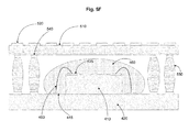
- Fig. 5F illustrates an assembled die-attach substrate 420 and interposer substrate 510 for a wire bonded IC 410 to form another type of reconstituted semiconductor package. Since the active surface of the IC 410 is facing the interposer substrate 510, the interposer substrate 510 is not connected or adhered to the IC 410.
- the solder ballss 550 are of a sufficient size to hold the interposer substrate 510 above the IC 410.
- An additional embodiment includes copper posts or solder columns in lieu of solder balls 550 to insure adequate height of the interposer substrate 510 above the IC 410.
- a tacking material can be used to temporarily hold the solder balls or copper posts 550 in place with their respective die-attach substrates 420 until a reflow process permanently connects the solder balls 550 to the two substrates.
- Fig. 5E for a flip chip IC and Fig. 5F for a wire bonded IC are given for exemplary purposes only.
- Another type of IC that can be used with embodiments described herein is an IC mounted to a lead frame, either with or without a die pad.
- MEMS micro-electro-mechanical system
- opto-electronic devices can be integrated into a reconstituted semiconductor package, according to embodiments described herein.
- solder bumps 430 are reflow connected to the die-attach substrate 420 (see Fig. 4A )
- the solder balls 550 are reflow connected to the interposer substrate 510 (see Fig. 5C )
- the solder balls 550 are reflow connected to the die-attach substrate 420 (see Fig. 5E ).
- Fig. 7A illustrates multiple assembled packages 710 affixed to a reconstitution carrier 720.
- Each assembled package 710 comprises an IC mounted to a die-attach substrate at a first surface of the IC, and an interposer substrate mounted over a second surface of the IC, wherein the interposer substrate is electrically and mechanically connected to the die-attach substrate.
- the assembled packages 710 may contain the same type of IC or different types of ICs.
- Fig. 7B illustrates a top view of the reconstitution carrier 720 in which individual assembled packages 710 are spaced apart in a rectangular array on the reconstitution carrier 720.
- a rectangular panel carrier is illustrated; however, other configured carriers are within the scope of the described embodiments, such as a square panel carrier or a long and narrow strip carrier.
- the reconstitution carrier 720 may have a variety of materials that is suitable for holding and transporting the array of assembled packages 710.
- Carrier materials may include, but are not limited to adhesion tape, ceramic, glass, plastic, semiconductor material, metal, or other material.
- An adhesive material can be applied to a surface of the carrier and/or to surfaces of the assembled packages 710.
- An adhesive material may include, but is not limited to epoxy or an adhesive film.
- an adhesive tape is used to maintain the positions of the assembled packages 710 during processing.
- the adhesive tape can be a panel configuration, such as the reconstitution carrier 720, or it can be a roll or strip of adhesive tape for receiving the array of assembled packages 710.
- Fig. 8A illustrates the assembled packages 710 attached to the reconstitution carrier 720.
- the reconstitution carrier 720 can be marked at positions where each assembled package 710 is to be placed. The markings can be optically located for correct placement of the assembled packages 710 onto the reconstitution carrier 720.
- a molding film 810 is pressed to the top surfaces of the assembled packages 710. Film 810 typically does not have cuts or openings.
- holes such as 820 can be made and spaced on the molding film 810 for the purpose of allowing a molding compound 830 to reach within the assembled packages 710, as well as reach in-between individual assembled packages 710. In an embodiment, holes 820 are placed at positions in-between the individual assembled packages 710.
- the molding compound 830 is under vacuum to facilitate movement of the molding compound 830 to reach all open spaces within and in-between the assembled packages 710.
- the molding film 810 on top of the assembled packages 710 keeps the contact pads on the upper surfaces of the interposer substrates clean and free from any molding compound 830.
- the reconstitution carrier 720 on the bottom of the assembled packages 710 keeps the contact pads on the lower surfaces of the die-attach substrates clean and free from any molding compound 830.
- Fig. 8B illustrates removal of the molding film 810 and the reconstitution carrier 720.
- An adhesive tape type of reconstitution carrier 720 can be removed by mechanical de-taping or applying UV light to reconstitution carrier 720 to deactivate the adhesive nature of the tape.
- Solder balls 840 are attached to the contact pads on the bottom surfaces of the die-attach substrates to form a ball grid array (BGA) of each assembled package 710. Solder flux can be applied to the contact pads of the die-attach substrate to hold the solder balls 840 in place until reflowing is completed.
- BGA ball grid array
- Embodiments for a reconstituted semiconductor package can be applied to most types of semiconductor packages, such as but not limited to fine-pitch ball grid arrays (FBGA), pin grid arrays (PGA), column grid arrays (CGA), land grid arrays (LGA), z-interconnect arrays, as well as others.
- FBGA fine-pitch ball grid arrays
- PGA pin grid arrays
- CGA column grid arrays
- LGA land grid arrays
- z-interconnect arrays as well as others.
- the reconstitution carrier 720 illustrated in Fig. 8A can be made of a polymer or photoimageable material, which can be patterned when exposed to ultraviolet (UV) light.
- a solder mask containing a plurality of openings that match the contact pads on the bottom surfaces of the die-attach substrates is placed over the reconstitution carrier 720. UV light exposes the reconstitution carrier 720 through the openings in the solder mask. The exposed areas of the reconstitution carrier 720 are removed. The solder balls are placed within the openings over the contact pads. A reflow process mechanically and electrically connects the solder balls to their respective contact pads.
- solder paste (a mixture of solder and flux) that is screen printed into the openings using a solder applicator.
- a reflow process causes the solder paste to reflow and connect the resulting solder balls or bumps to their respective contact pads.
- the reconstitution carrier 720 can be removed after the reflow process, or it can remain on the bottom side of the die-attach substrate.
- Fig. 8C illustrates the assembled and molded packages singulated into individual reconstitution semiconductor packages 800.
- the singulation can be implemented by cutting, sawing, laser slicing, or any other method of cutting through molding compound.
- singulation occurs only through the molding compound. There is no cutting through either the interposer substrate or the die-attach substrate when the interposer substrate and the die-attach substrate are approximately the same size and the molding compound extends beyond the perimeters of the substrates.
- the interposer substrates mounted to their respective die-attach substrates are separated from one another to form a gap between the packages (see Figs. 7A-8B ). Therefore, there is no cutting of either substrate, and as a result, there is no wasted substrate material from the singulation process. Also, the molding along the edges of the substrates will increase the protection of the final package.
- Fig. 9A illustrates a variation of the process illustrated in Fig. 5D , where an adhesive 560 was applied to the back side of the IC 410. The adhesive 560 was also adhered to the interposer substrate 510 when the interposer substrate 510 was mounted to the die-attach substrate 420.
- Fig. 9A illustrates an absence of adhesive between the IC and the interposer substrate. Instead, the molding compound 830 fills the gap between the IC and the interposer substrate. A vacuum molding process helps to insure that the molding compound reaches all open spaces within the package.
- Fig. 9B illustrates the same device and process illustrated in Fig. 9A , in addition to substituting molding compound 830 for the capillary underfill material between the IC and the die-attach substrate.
- a vacuum molding process helps to insure that the molding compound reaches all open spaces within the package.
- Fig. 10A is an illustration of an interposer package-on-package semiconductor device 1000 according to embodiments described herein.
- An interposer substrate 1090 is mounted to a die-attach substrate 1030 by means of solder balls 1270a.
- the solder balls 1270a are connected to the bottom surface 1120b of the interposer substrate 1090 by means of contact pads 1300b, and the solder balls 1270a are connected to the top surface 1060a of the die-attach substrate 1030 by means of contact pads 1300a.
- a flip chip integrated circuit 1150 is connected to the top surface 1060a of the die-attach substrate 1030 by means of contact pads 1300d.
- a molding compound 1240 is filled within all open spaces between the interposer substrate 1090 and the die-attach substrate 1030, as well as along the edges of the connected interposer substrate 1090 and the die-attach substrate 1030.
- External solder balls 1270b are attached to the bottom surface 1060b of the die-attach substrate 1030 by means of contact pads 1300c.
- Additional devices such as a surface mount device 1210 and a flip chip device 1180 are connected to the top surface 1120a of the interposer substrate 1090 by means of contact pads 1300.
- Fig. 10B is an illustration of a flip chip IC 1030 connected to a die-attach substrate 1020, and an interposer substrate 1010 connected to the die-attach substrate 1020 by solder balls 1040.
- Encapsulation 1050 is filled in between the interposer substrate 1010 and the die-attach substrate 1020 and around the IC. The encapsulation 1050 is also filled around the sides of both substrates. However, the interposer substrate 1010 is smaller than the die-attach substrate.
- Fig. 10C a similar flip chip package is illustrated, in which the interposer substrate 1010 is larger than the die-attach substrate 1020.
- the flip chip packages of Figs. 10B and 10C would have solder balls connected to the bottom surface of the die-attach substrate 1020, as illustrated in earlier figures.
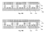
- Fig. 10D is an illustration of a plurality of die-attach substrates 1020, with associated flip chip ICs 1030 connected thereto, as well as associated interposer substrates 1010 connected to the die-attach substrates 1020 by solder columns or conductive posts 1040.
- Encapsulation 1050 is filled in between the interposer substrates 1010 and the die-attach substrates 1020.
- the die-attach substrates 1020 are abutted next to each other, so the encapsulation 1050 only resides along the sides of the interposer substrates 1010 and not along the sides of the die-attach substrates 1020.
- the die-attach substrates 1020 may be previously singulated, tested, and grouped together on a carrier, such as previously described.
- the die-attach substrate 1020 may be one whole substrate or wafer, which is singulated during the final singulation process to form the individual packages.
- Fig. 10E is similar to the packages illustrated in Fig. 10D , except the interposer substrates 1010 are abutted next to each other, so the encapsulation 1050 only resides along the sides of the die-attach substrates 1020 and not along the sides of the interposer substrates 1010.
- the interposer substrates 1010 may be previously singulated, tested, and grouped together on a carrier, such as previously described.
- the interposer substrate 1010 may be one whole substrate or wafer, which is singulated during the final singulation process to form the individual packages.
- Fig. 11 is a flowchart for a method of forming a semiconductor package 1100, such as a reconstituted interposer package-on-package.
- An array of die-attach substrates is formed onto a carrier in step S1110.
- the array of individual die-attach substrates may contain reconstituted working substrates, wherein the substrates were previously tested and only the working substrates are held for further processing.
- the carrier may be comprised of an adhesive carrier.
- a semiconductor device is mounted onto a first surface of each of the die-attach substrates in step S 1120.
- the semiconductor device is a flip chip device.
- the semiconductor device is a wire bonded device.
- Solder ball connections are formed to a plurality of interposer substrates in step S 1125.
- Each interposer substrate is mounted over a respective semiconductor device in step S 1130.
- the interposer substrates are electrically and mechanically connected to the first surface of the respective die-attach substrates, via the solder ball connections in step S1140.
- the die-attach substrate and the interposer substrate are approximately the same size.
- the die-attach substrate is larger than the interposer substrate.
- the die-attach substrate is smaller than the interposer substrate.
- a molding compound is filled in open spaces within and between the interposer substrates mounted to their respective die-attach substrates to form an array of reconstituted semiconductor packages in step S1150.
- the array of packages has a gap between each of the die-attach substrates and their respective mounted interposer substrates.
- the molding compound fills the gaps between each reconstituted semiconductor package of a die-attach substrate and mounted interposer substrate.
- Electrical connections are mounted to a second surface of the die-attach substrates in step S1160.
- the electrical connections are mounted in a grid array pattern.
- the array of reconstituted semiconductor packages are singulated through the molding compound between each of the die-attach substrates and respective mounted interposer substrates in step S1170. The singulation cuts through the molding compound only. Since there is a gap between each pair of die-attach substrates and respective mounted interposer substrates, neither substrate is cut by the singulation process.
- preparation of the interposer substrate and electrical connections could be executed before preparation of the IC and die-attach substrate connections.
- the interposer substrate processing could be con-current with the IC and die-attach substrate processing.
- Embodiments described herein for a reconstituted interposer semiconductor package can be used in many applications, including but not limited to the networking, mobile, wireless, wearable electronics, and broadband.
- the reconstituted interposer semiconductor package described herein can be used in multi-core processors, knowledge-based processors, server message block (SMB) processors, encryption coprocessors, and security processors.
- SMB server message block
- the reconstituted interposer semiconductor package described herein can be used in 3G baseband processors, LTE baseband processors, mobile video processors, mobile graphics processors, application processors, touch controllers, wireless power, Internet of things (IoT) and wearable system-on-chips (SoCs), wireless video, and antennas.
- 3G baseband processors LTE baseband processors
- mobile video processors mobile graphics processors
- application processors touch controllers
- wireless power Internet of things (IoT) and wearable system-on-chips (SoCs)
- IoT Internet of things
- the reconstituted interposer semiconductor package described herein can be used in cable set-top boxes (STBs), satellite STBs, Internet Protocol (IP) STBs, terrestrial STBs, ultra high definition (HD) processors, STB graphics processors, and STB security processors.
- STBs cable set-top boxes
- IP Internet Protocol
- HD ultra high definition
- STB graphics processors STB graphics processors
- STB security processors STB security processors.
- a reconstituted semiconductor package and a method of making a reconstituted semiconductor package are described.
- An array of die-attach substrates is formed onto a carrier.
- a semiconductor device is mounted onto a first surface of each of the die-attach substrates.
- An interposer substrate is mounted over each of the semiconductor devices.
- the interposer substrates are electrically connected to the first surface of the respective die-attach substrates.
- a molding compound is filled in open spaces within and between the interposer substrates mounted to their respective die-attach substrates to form an array of reconstituted semiconductor packages. Electrical connections are mounted to a second surface of the die-attach substrates.
- the array of reconstituted semiconductor packages is singulated through the molding compound between each of the die-attach substrates and respective mounted interposer substrates.
Landscapes
- Structures Or Materials For Encapsulating Or Coating Semiconductor Devices Or Solid State Devices (AREA)
- Wire Bonding (AREA)
- Engineering & Computer Science (AREA)
- Microelectronics & Electronic Packaging (AREA)
- Combinations Of Printed Boards (AREA)
- Encapsulation Of And Coatings For Semiconductor Or Solid State Devices (AREA)
Abstract
Description
- This application claims priority to
U.S. Provisional Application Number 62/001,367 filed May 21, 2014 - A semiconductor package can be a metal, plastic, glass, or ceramic casing containing one or more semiconductor electronic components, also referred to as dies or integrated circuits (ICs). The package provides protection against impact and corrosion, as well as environmental factors, such as moisture, oxidation, heat, and contaminants. Electrical contacts or leads emminate from the package and are connected to other devices and/or to an intermediary substrate, or directly to a circuit board. The package may have as few as two leads or contacts for devices such as diodes, or have several hundred leads or contacts in the case of a microprocessor.
- The semiconductor package can be a special purpose self-contained device, which can be mounted to a printed circuit board (PCB) or a printed wiring board (PWB) of an end product. ICs can be connected to a substrate in a variety of layouts, as well as stacked in multiple layers. In addition, packages can be mounted upon other packages to form a package-on-package device.
- User products are becoming more complicated with several features and functions. In addition, many user products are becoming smaller, especially wireless devices. As a result, manufacturers are utilizing packaging alternatives as a way of achieving more features and functions in a smaller area.
- Embodiments include a reconstituted semiconductor package, which has an array of individual die-attach substrates on a carrier. The package also has a plurality of semiconductor devices, each mounted and electrically connected to a first surface of an associated die-attach substrate. The package also has a plurality of individual interposer substrates, each mounted over an associated semiconductor device and electrically connected to the first surface of the associated die-attach substrate. The package also has an encapsulation (for example, a molding compound) filled within open spaces between and around each of the interposer substrates mounted to its associated die-attach substrate to form a plurality of reconstituted semiconductor packages. The package has electrical connections mounted to a second surface of each of the die-attach substrates. Singulation of each of the reconstituted semiconductor packages cuts through the molding compound and between each of the die-attach substrates and respective mounted interposer substrates.
- Embodiments also include a method of forming a semiconductor package. The method includes forming an array of die-attach substrates onto a carrier, and mounting a semiconductor device onto a first surface of each of the die-attach substrates. The method also includes forming solder ball or conductive post connections to a plurality of interposer substrates, mounting each interposer substrate over a respective semiconductor device, and electrically connecting the interposer substrates to the first surface of the respective die-attach substrates, via the solder ball or conductive post connections. The method also includes filling a molding compound in open spaces within and between the interposer substrates mounted to their respective die-attach substrates to form an array of reconstituted semiconductor packages. The method also includes mounting electrical connections to a second surface of the die-attach substrates, and singulating the array of reconstituted semiconductor packages through the molding compound between each of the die-attach substrates and respective mounted interposer substrates.
- Embodiments also include a reconstituted interposer package. The reconstituted interposer package has an interposer substrate electrically mounted to a first surface of a reconstituted die-attach substrate and straddling over an integrated circuit mounted on the first surface of the reconstituted die-attach substrate. The interposer package also has a molding compound filled within open spaces between the interposer substrate and the first surface of the reconstituted die-attach substrate. Singulated surfaces of the molding compound also reside along edges of the interposer substrate mounted to the reconstituted die-attach substrate. The reconstituted interposer package has external electrical connections formed in a grid array on a second surface of the reconstituted die-attach substrate.
- The foregoing paragraphs have been provided by way of general introduction, and are not intended to limit the scope of the following claims. The described embodiments, together with further advantages, will be best understood by reference to the following detailed description taken in conjunction with the accompanying drawings.
- A more complete appreciation of the disclosure and many of the attendant advantages thereof will be readily obtained as the same becomes better understood by reference to the following detailed description when considered in connection with the accompanying drawings, wherein:
-
Figs. 1A-1B are illustrations of an IC wafer and an individual singulated IC, according to an example; -
Figs. 2A-2B are illustrations of bonding pad patterns on an active surface of an IC according to an example; -
Figs. 3A-3B are illustrations of a substrate panel and an individual die-attach substrate according to an example; -
Figs. 4A-4B are illustrations of an IC solder-bump attached to a die-attach substrate according to an example; -
Fig. 4C is an illustration of an IC wire-bonded to a die-attach substrate according to an example; -
Figs. 5A-5B are illustrations of a substrate panel and an individual interposer substrate according to an example; -
Fig. 5C is an illustration of an interposer substrate formation according to an example; -
Figs. 5D-5E are illustrations of connecting an interposer substrate to a die-attach substrate containing a flip chip IC according to an example; -
Fig. 5F is an illustration of an interposer substrate connected to a die-attach substrate containing a wire-bonded IC according to an example; -
Fig. 6 contains illustrations of die-attach adhesive patterns according to an example; -
Figs. 7A-7B are illustrations of reconstituted packages mounted to a carrier according to an example; -
Fig. 8A illustrates a molding compound filled within and around the reconstituted packages according to an example; -
Fig. 8B illustrates removal of the molding film and carrier, and solder ball external connections according to an example; -
Fig. 8C illustrates singulation of the reconstituted packages according to an example; -
Fig. 9A illustrates molding compound in place of die-attach adhesive according to an example; -
Fig. 9B illustrates molding compound in place of die-attach adhesive and die underfill according to an example; -
Figs. 10A-10E illustrate reconstituted interposer semiconductor packages according to some examples; and -
Fig. 11 is a flowchart for a method of forming a semiconductor package according to an example. - Referring now to the drawings, wherein like reference numerals designate identical or corresponding parts throughout the several views.
- Multiple ICs can be assembled on a substrate and be interconnected with wire bonds and/or a metal pattern to form a package. An example of a multi-chip IC package is an application microprocessor, which may include separate ICs for such things as memory within the same package.
- ICs can be manufactured in wafer level form, in which 10s, 100s, or 1000s of ICs are formed within a single semiconductor wafer. The wafer material may be silicon, gallium arsenide, or other semiconducting material.
Fig. 1A illustrates awafer 100 containingmultiple ICs 110. TheICs 110 can be square or rectangular in shape, as well as other shapes suited to a particular manufacturing process. TheICs 110 are separated from one another in a singulation process, which can be implemented by scribing the boundaries between theindividual ICs 110, then sawing, breaking, or cutting theICs 110 apart. -
Fig. 1B illustrates a cross sectional area of anIC 110. TheIC 110 has aninactive surface 120 and anactive surface 130. Theactive surface 130 has a plurality of electrically conductive contact regions orcontact pads 140, which are designed to interconnect theIC 110 with other devices or substrates. An IC contact pad can have multiple layers, referred to as under-bump metallization (UBM). The base conductive layer may contain aluminum. Since solder material does not adhere well to aluminum, another metallic or conductive layer can be patterned over the aluminum pad. An example UBM may include a combination of aluminum, nickel vanadium, and copper. However, several other UBM materials are contemplated by embodiments described herein. A contact pad, referred to herein may include a UBM layer. - The
contact pads 140 can be arranged in various configurations, depending upon the medium in which it will be connected to another device or substrate.Fig. 2A illustrates a top view ofIC 110, showingmultiple contact pads 140 arranged primarily in the center of theactive surface 130 of theIC 110. This configuration can be used for a flip chip type of device, in which the device can have solder bumps or copper pillars connected to thecontact pads 140. The flip chip device and connected solder bumps are "flipped over" and connected to contact pads of another device or substrate.Fig. 2B illustrates a top view ofIC 110, showingmultiple contact pads 140 arranged primarily around the perimeter of theactive surface 130 of theIC 110. This configuration can be used for a wire bonded type of device. The wire bonded device is attached, such as stacked devices or side-by-side wire bonded devices. Bonding wires connect thecontact pads 140 of the wire bonded device to contact pads of another device or substrate. - Embodiments described herein include attaching individual ICs to a substrate.
Fig. 3A illustrates asubstrate panel 300, which can be used to form multiple die-attach substrates, shown individually as 310. Thesubstrate panel 300 can be made of a material, such as flex tape material, ceramic material, organic laminate material, resin-based material, lead frame, or other similar materials in which one ormore ICs 110 can be supported. Thesubstrate panel 300 is formed to include one or more routing layers and one or more electrically insulating layers. Electrically conductive vias are formed through the electrically insulating layers. Conductive contact pads on a first surface of thesubstrate panel 300 are connected through thesubstrate panel 300 by routing layers and vias to contact pads on a second surface of thesubstrate panel 300. - The
substrate panel 300 is separated into individual die-attachsubstrates 310, which can be singulated similar to thewafer 100 singulation described above.Fig. 3B illustrates a cross section of an exemplary individual die-attachsubstrate 310. The die-attachsubstrate 310 has metallization orcontact pads 320 patterned on a first surface.Conductive vias 330 are formed through the die-attachsubstrate 310 and are electrically connected to contactpads 340 located on a second surface of the die-attachsubstrate 310. The die-attachsubstrate 310 provides an interface to connect one ormore ICs 110 on an upper surface, having a particular pattern of interconnecting contact pads to a PCB, for example having a different pattern of interconnecting contact pads or metallization. In an example, thelower contact pads 340 can be patterned to match a standard or commonly used PCB pattern. - After singulating the
substrate panel 300 into individual die-attachsubstrates 310, the individual die-attachsubstrates 310 are tested and sorted into working substrates and failed substrates. Testing may include, but is not limited to functional tests by applying probes to conductive features of substrates to provide test signals and to measure test results. Environmental tests may also be performed, such as exposure to moisture, extreme temperatures, and shock. Die-attachsubstrates 310 that are determined to be non-working can be marked by an ink mark, a laser marking, or other type of mark for later identification as a non-working substrate. This provides the advantage of continued processing with only good working substrates. The failed substrates are removed early in the process before investing further materials and resources. The substrate testing may also be performed inpanel 300 before singulation. -
Fig. 4A illustrates anIC 410 in an inverted position withsolder bumps 430 facing downward towards a die-attachsubstrate 420. TheIC 410 is a flip chip, in which solder bumps 430 have been attached to the active surface of theIC 410. The solder bumps 430 may contain a metal core, such as copper with an outside solder film. The solder bumps 430 may also contain a solder material throughout, such as a tin/silver solder with no metal core. The solder bumps 430 may also be a copper post with tips coated with tin/silver solder.Fig. 4B illustrates the solder bumps 430 on theIC 410 are attached to contact pads on an upper surface of the die-attachsubstrate 420. A tacking material can be used to temporarily hold theICs 410 in place with their respective die-attachsubstrates 420. For instance, solder flux can be applied to the contact pads to hold the solder bumps 430 in place until reflowing is completed.Figs. 4A and 4B illustrate just oneIC 410 and one mating die-attachsubstrate 420 for simplicity. However,ICs 410 are mated to each of the working die-attachsubstrates 420 on a reconstitution carrier. The entire reconstitution carrier of die-attachsubstrates 420 and matedICs 410 is exposed to a reflow process, at a temperature above the reflow temperature of the solder bumps 430. The reflow process mechanically and electrically connects eachIC 410 to its respective die-attachsubstrate 420. In an embodiment, acapillary underfill material 440 can be used to encapsulate the solder bumps 430 between eachIC 410 and its respective die-attachsubstrate 420. Thecapillary underfill material 440 is an insulative and non-conducting material used to protect the solder bump connections from oxidation and other environmental and physical elements. -
Fig. 4C illustrates anIC 410 connected to a die-attachsubstrate 420 in a face-up position. The inactive surface of theIC 410 is attached to the die-attachsubstrate 420 by an adhesive material. The active surface of theIC 410 containscontact pads 435, which are connected to contactpads 445 on the die-attachsubstrate 420 by bondingwires 450. Thebonding wires 450 may be made of an oxidation-resistant material, such as gold, palladium-coated copper, or silver. In an embodiment, aninsulative encapsulation material 460 can be formed over thebonding wires 450 andcontact pads 435 of theIC 410 andcontact pads 445 of the die-attachsubstrate 420 to protect thebonding wires 450 and respective contact pads from physical and environmental elements. Theoptional encapsulation material 460 may be applied by means of a glob top process, as an example. Glob-top materials, such as silicone or an epoxy having high viscosity, such that it can be applied to a substantially planar surface without being laterally confined. However, other methods of encapsulating bonding wires and associated contact pads are contemplated by embodiments described herein. Theencapsulation material 460 also provides an advantage of preventing wire sweep in a future molding process. Theencapsulation material 460 over thebonding wires 450 prevents thebonding wires 450 from touching one another when a molding material flows over theIC 410.Fig. 4C illustrates just oneIC 410 and one mating die-attachsubstrate 420 for simplicity. However,ICs 410 are mated to each of the working die-attachsubstrates 420 on a reconstitution carrier. -
Figs. 5A-5F illustrate a process of forming and integrating an interposer substrate, as used in embodiments described herein. The materials and processing can be similar to the die-attach substrate processing discussed above with reference toFigs. 3A-3B .Fig. 5A illustrates asubstrate panel 500, which can be used to form multiple interposer substrates, shown individually as 510. Thesubstrate panel 500 can be made of a material, such as flex tape material, ceramic material, organic laminate material, resin-based material, lead frame, or other similar materials. Thesubstrate panel 500 is separated intoindividual interposer substrates 510, which can be singulated in a similar process as thewafer 100 singulation process described above. -
Fig. 5B illustrates a cross section of an exemplaryindividual interposer substrate 510. Theinterposer substrate 510 has metallization orcontact pads 520 patterned on a first surface.Conductive vias 530 are formed through theinterposer substrate 510 and are electrically connected to contactpads 540 located on a second surface of theinterposer substrate 510. Theconductive vias 530 redirect theupper contact pads 520, patterned to receive additional devices or substrates to thelower contact pads 540, patterned to connect with a die-attach substrate, for example. -
Fig. 5C illustratessolder balls 550 being connected to contactpads 540 on the second surface of theinterposer substrate 510. Thesolder balls 550 can be temporarily held in place by a tacking material, such as solder flux during processing. Thesolder balls 550 are mechanically and electrically connected to thecontact pads 540 of theinterposer substrate 510 by exposing the combinedinterposer substrate 510 andsolder balls 550 to a temperature above the reflow temperature of thesolder balls 550. -
Fig. 5D illustrates how theinterposer substrate 510 will be mounted over anIC 410 to a die-attachsubstrate 420. Thesolder balls 550 straddle theIC 410 located in the center of the die-attachsubstrate 420. Thesolder balls 550 are of a sufficient size to hold theinterposer substrate 510 above theIC 410 when mounted.Fig. 5D illustrates aflip chip IC 410, in which the inactive surface of theIC 410 will be connected to the second surface of theinterposer substrate 510. An adhesive 560 has been applied to the inactive surface of theIC 410. The adhesive 560 may include, but is not limited to an adhesive paste, a die-attach film, an epoxy solder flux, or other adhesive materials with properties that are suited for the adjoining materials of theIC 410 and theinterposer substrate 510, and are suited for the operating temperatures of theIC 410. The adhesive 560 can be applied to the inactive surface of theIC 410 and/or the second surface of theinterposer substrate 510 in a variety of patterns, as illustrated inFig. 6 . Other patterns of adhesive application are contemplated by embodiments described herein. The particular pattern may depend upon factors, such as but not limited to size of theIC 410, power level of theIC 410, heat dissipation of theIC 410, environmental exposure, intended use of the final semiconductor package, as well as other factors. -
Fig. 5E illustrates aninterposer substrate 510 mounted to a die-attachsubstrate 420 with aflip chip IC 410 mounted thereon to form a reconstituted semiconductor package. A tacking material, such as solder flux can be used to temporarily hold thesolder balls 550 in place with contact pads of their respective die-attachsubstrates 420. Theinterposer substrate 510 is also adhered to the back side of theflip chip IC 410. The combined structure ofFig. 5E is exposed to a reflow process to mechanically and electrically connect thesolder balls 550 to the contact pads of the die-attach substrate 420 (not shown inFig. 5E ). The adhesive 560 can be cured during the reflow process, or an additional process can be implemented to cure the adhesive 560, preferably after the reflow process. In an embodiment, theinterposer substrate 510 and theIC 410 can be attached in one reflow process. -
Fig. 5F illustrates an assembled die-attachsubstrate 420 andinterposer substrate 510 for a wire bondedIC 410 to form another type of reconstituted semiconductor package. Since the active surface of theIC 410 is facing theinterposer substrate 510, theinterposer substrate 510 is not connected or adhered to theIC 410. Thesolder ballss 550 are of a sufficient size to hold theinterposer substrate 510 above theIC 410. An additional embodiment includes copper posts or solder columns in lieu ofsolder balls 550 to insure adequate height of theinterposer substrate 510 above theIC 410. A tacking material can be used to temporarily hold the solder balls orcopper posts 550 in place with their respective die-attachsubstrates 420 until a reflow process permanently connects thesolder balls 550 to the two substrates. -
Fig. 5E for a flip chip IC andFig. 5F for a wire bonded IC are given for exemplary purposes only. Another type of IC that can be used with embodiments described herein is an IC mounted to a lead frame, either with or without a die pad. With some adjustments, micro-electro-mechanical system (MEMS) devices and opto-electronic devices can be integrated into a reconstituted semiconductor package, according to embodiments described herein. - In the assembly process illustrated in
Figs. 4A-5F , there are multiple reflow processes. For theflip chip IC 410, the solder bumps 430 are reflow connected to the die-attach substrate 420 (seeFig. 4A ), thesolder balls 550 are reflow connected to the interposer substrate 510 (seeFig. 5C ), and thesolder balls 550 are reflow connected to the die-attach substrate 420 (seeFig. 5E ). - The reconstituted semiconductor packages described above can be prepared for mold-injection, according to embodiments described herein.
Fig. 7A illustrates multiple assembledpackages 710 affixed to areconstitution carrier 720. Each assembledpackage 710 comprises an IC mounted to a die-attach substrate at a first surface of the IC, and an interposer substrate mounted over a second surface of the IC, wherein the interposer substrate is electrically and mechanically connected to the die-attach substrate. The assembled packages 710 may contain the same type of IC or different types of ICs. -
Fig. 7B illustrates a top view of thereconstitution carrier 720 in which individual assembledpackages 710 are spaced apart in a rectangular array on thereconstitution carrier 720. A rectangular panel carrier is illustrated; however, other configured carriers are within the scope of the described embodiments, such as a square panel carrier or a long and narrow strip carrier. Thereconstitution carrier 720 may have a variety of materials that is suitable for holding and transporting the array of assembledpackages 710. Carrier materials may include, but are not limited to adhesion tape, ceramic, glass, plastic, semiconductor material, metal, or other material. An adhesive material can be applied to a surface of the carrier and/or to surfaces of the assembled packages 710. An adhesive material may include, but is not limited to epoxy or an adhesive film. In an embodiment, an adhesive tape is used to maintain the positions of the assembledpackages 710 during processing. The adhesive tape can be a panel configuration, such as thereconstitution carrier 720, or it can be a roll or strip of adhesive tape for receiving the array of assembledpackages 710. -
Fig. 8A illustrates the assembledpackages 710 attached to thereconstitution carrier 720. Thereconstitution carrier 720 can be marked at positions where each assembledpackage 710 is to be placed. The markings can be optically located for correct placement of the assembledpackages 710 onto thereconstitution carrier 720. Amolding film 810 is pressed to the top surfaces of the assembled packages 710.Film 810 typically does not have cuts or openings. Alternatively, holes such as 820 can be made and spaced on themolding film 810 for the purpose of allowing amolding compound 830 to reach within the assembledpackages 710, as well as reach in-between individual assembled packages 710. In an embodiment, holes 820 are placed at positions in-between the individual assembled packages 710. In another embodiment, themolding compound 830 is under vacuum to facilitate movement of themolding compound 830 to reach all open spaces within and in-between the assembled packages 710. Themolding film 810 on top of the assembledpackages 710 keeps the contact pads on the upper surfaces of the interposer substrates clean and free from anymolding compound 830. Likewise, thereconstitution carrier 720 on the bottom of the assembledpackages 710 keeps the contact pads on the lower surfaces of the die-attach substrates clean and free from anymolding compound 830. -
Fig. 8B illustrates removal of themolding film 810 and thereconstitution carrier 720. An adhesive tape type ofreconstitution carrier 720 can be removed by mechanical de-taping or applying UV light toreconstitution carrier 720 to deactivate the adhesive nature of the tape.Solder balls 840 are attached to the contact pads on the bottom surfaces of the die-attach substrates to form a ball grid array (BGA) of each assembledpackage 710. Solder flux can be applied to the contact pads of the die-attach substrate to hold thesolder balls 840 in place until reflowing is completed. Embodiments for a reconstituted semiconductor package can be applied to most types of semiconductor packages, such as but not limited to fine-pitch ball grid arrays (FBGA), pin grid arrays (PGA), column grid arrays (CGA), land grid arrays (LGA), z-interconnect arrays, as well as others. - Another embodiment includes using the
reconstitution carrier 720 illustrated inFig. 8A as a solder stencil. Thereconstitution carrier 720 can be made of a polymer or photoimageable material, which can be patterned when exposed to ultraviolet (UV) light. A solder mask containing a plurality of openings that match the contact pads on the bottom surfaces of the die-attach substrates is placed over thereconstitution carrier 720. UV light exposes thereconstitution carrier 720 through the openings in the solder mask. The exposed areas of thereconstitution carrier 720 are removed. The solder balls are placed within the openings over the contact pads. A reflow process mechanically and electrically connects the solder balls to their respective contact pads. Another embodiment provides a solder paste (a mixture of solder and flux) that is screen printed into the openings using a solder applicator. A reflow process causes the solder paste to reflow and connect the resulting solder balls or bumps to their respective contact pads. Thereconstitution carrier 720 can be removed after the reflow process, or it can remain on the bottom side of the die-attach substrate. -
Fig. 8C illustrates the assembled and molded packages singulated into individual reconstitution semiconductor packages 800. The singulation can be implemented by cutting, sawing, laser slicing, or any other method of cutting through molding compound. By exercising embodiments described herein, singulation occurs only through the molding compound. There is no cutting through either the interposer substrate or the die-attach substrate when the interposer substrate and the die-attach substrate are approximately the same size and the molding compound extends beyond the perimeters of the substrates. The interposer substrates mounted to their respective die-attach substrates are separated from one another to form a gap between the packages (seeFigs. 7A-8B ). Therefore, there is no cutting of either substrate, and as a result, there is no wasted substrate material from the singulation process. Also, the molding along the edges of the substrates will increase the protection of the final package. -
Fig. 9A illustrates a variation of the process illustrated inFig. 5D , where an adhesive 560 was applied to the back side of theIC 410. The adhesive 560 was also adhered to theinterposer substrate 510 when theinterposer substrate 510 was mounted to the die-attachsubstrate 420.Fig. 9A illustrates an absence of adhesive between the IC and the interposer substrate. Instead, themolding compound 830 fills the gap between the IC and the interposer substrate. A vacuum molding process helps to insure that the molding compound reaches all open spaces within the package. -
Fig. 9B illustrates the same device and process illustrated inFig. 9A , in addition to substitutingmolding compound 830 for the capillary underfill material between the IC and the die-attach substrate. A vacuum molding process helps to insure that the molding compound reaches all open spaces within the package. -
Fig. 10A is an illustration of an interposer package-on-package semiconductor device 1000 according to embodiments described herein. Aninterposer substrate 1090 is mounted to a die-attachsubstrate 1030 by means ofsolder balls 1270a. Thesolder balls 1270a are connected to thebottom surface 1120b of theinterposer substrate 1090 by means ofcontact pads 1300b, and thesolder balls 1270a are connected to thetop surface 1060a of the die-attachsubstrate 1030 by means ofcontact pads 1300a. A flip chip integratedcircuit 1150 is connected to thetop surface 1060a of the die-attachsubstrate 1030 by means ofcontact pads 1300d. Amolding compound 1240 is filled within all open spaces between theinterposer substrate 1090 and the die-attachsubstrate 1030, as well as along the edges of the connectedinterposer substrate 1090 and the die-attachsubstrate 1030.External solder balls 1270b are attached to thebottom surface 1060b of the die-attachsubstrate 1030 by means ofcontact pads 1300c. Additional devices such as asurface mount device 1210 and aflip chip device 1180 are connected to thetop surface 1120a of theinterposer substrate 1090 by means ofcontact pads 1300. -
Fig. 10B is an illustration of aflip chip IC 1030 connected to a die-attachsubstrate 1020, and aninterposer substrate 1010 connected to the die-attachsubstrate 1020 bysolder balls 1040.Encapsulation 1050 is filled in between theinterposer substrate 1010 and the die-attachsubstrate 1020 and around the IC. Theencapsulation 1050 is also filled around the sides of both substrates. However, theinterposer substrate 1010 is smaller than the die-attach substrate. InFig. 10C , a similar flip chip package is illustrated, in which theinterposer substrate 1010 is larger than the die-attachsubstrate 1020. Although not illustrated, the flip chip packages ofFigs. 10B and 10C would have solder balls connected to the bottom surface of the die-attachsubstrate 1020, as illustrated in earlier figures. -
Fig. 10D is an illustration of a plurality of die-attachsubstrates 1020, with associatedflip chip ICs 1030 connected thereto, as well as associatedinterposer substrates 1010 connected to the die-attachsubstrates 1020 by solder columns orconductive posts 1040.Encapsulation 1050 is filled in between theinterposer substrates 1010 and the die-attachsubstrates 1020. The die-attachsubstrates 1020 are abutted next to each other, so theencapsulation 1050 only resides along the sides of theinterposer substrates 1010 and not along the sides of the die-attachsubstrates 1020. In an embodiment, the die-attachsubstrates 1020 may be previously singulated, tested, and grouped together on a carrier, such as previously described. In another embodiment, the die-attachsubstrate 1020 may be one whole substrate or wafer, which is singulated during the final singulation process to form the individual packages. -
Fig. 10E is similar to the packages illustrated inFig. 10D , except theinterposer substrates 1010 are abutted next to each other, so theencapsulation 1050 only resides along the sides of the die-attachsubstrates 1020 and not along the sides of theinterposer substrates 1010. In an embodiment, theinterposer substrates 1010 may be previously singulated, tested, and grouped together on a carrier, such as previously described. In another embodiment, theinterposer substrate 1010 may be one whole substrate or wafer, which is singulated during the final singulation process to form the individual packages. -
Fig. 11 is a flowchart for a method of forming asemiconductor package 1100, such as a reconstituted interposer package-on-package. An array of die-attach substrates is formed onto a carrier in step S1110. The array of individual die-attach substrates may contain reconstituted working substrates, wherein the substrates were previously tested and only the working substrates are held for further processing. The carrier may be comprised of an adhesive carrier. A semiconductor device is mounted onto a first surface of each of the die-attach substrates in step S 1120. In an embodiment, the semiconductor device is a flip chip device. In another embodiment, the semiconductor device is a wire bonded device. - Solder ball connections are formed to a plurality of interposer substrates in step S 1125. Each interposer substrate is mounted over a respective semiconductor device in
step S 1130. The interposer substrates are electrically and mechanically connected to the first surface of the respective die-attach substrates, via the solder ball connections in step S1140. In an embodiment, the die-attach substrate and the interposer substrate are approximately the same size. In another embodiment, the die-attach substrate is larger than the interposer substrate. In still another embodiment, the die-attach substrate is smaller than the interposer substrate. A molding compound is filled in open spaces within and between the interposer substrates mounted to their respective die-attach substrates to form an array of reconstituted semiconductor packages in step S1150. In an embodiment, the array of packages has a gap between each of the die-attach substrates and their respective mounted interposer substrates. As a result, the molding compound fills the gaps between each reconstituted semiconductor package of a die-attach substrate and mounted interposer substrate. - Electrical connections are mounted to a second surface of the die-attach substrates in step S1160. In an embodiment, the electrical connections are mounted in a grid array pattern. The array of reconstituted semiconductor packages are singulated through the molding compound between each of the die-attach substrates and respective mounted interposer substrates in step S1170. The singulation cuts through the molding compound only. Since there is a gap between each pair of die-attach substrates and respective mounted interposer substrates, neither substrate is cut by the singulation process.
- The methods and devices described herein are exemplary and are given to illustrate the features and processes of certain embodiments. Embodiments are not restricted to any particular order or to the exemplary order described herein. For example, preparation of the interposer substrate and electrical connections could be executed before preparation of the IC and die-attach substrate connections. As another example, the interposer substrate processing could be con-current with the IC and die-attach substrate processing.
- Embodiments described herein for a reconstituted interposer semiconductor package can be used in many applications, including but not limited to the networking, mobile, wireless, wearable electronics, and broadband. In the networking application, the reconstituted interposer semiconductor package described herein can be used in multi-core processors, knowledge-based processors, server message block (SMB) processors, encryption coprocessors, and security processors. In the mobile, wireless applications, and wearable applications, the reconstituted interposer semiconductor package described herein can be used in 3G baseband processors, LTE baseband processors, mobile video processors, mobile graphics processors, application processors, touch controllers, wireless power, Internet of things (IoT) and wearable system-on-chips (SoCs), wireless video, and antennas. In the broadband applications, the reconstituted interposer semiconductor package described herein can be used in cable set-top boxes (STBs), satellite STBs, Internet Protocol (IP) STBs, terrestrial STBs, ultra high definition (HD) processors, STB graphics processors, and STB security processors. These devices and systems can be used in products including but not limited to routers, smartphones, tablets, personal computers, and wearable devices such as watches, shoes, clothes, and glasses.
- The foregoing discussion discloses and describes merely exemplary embodiments of the present invention. As will be understood by those skilled in the art, the present invention may be embodied in other specific forms without departing from the spirit or essential characteristics thereof. Accordingly, the disclosure of the present embodiments is intended to be illustrative, but not limiting of the scope of the embodiments, as well as other claims. The disclosure, including any readily discernible variants of the teachings herein, define, in part, the scope of the foregoing claim terminology such that no subject matter is dedicated to the public.
- A reconstituted semiconductor package and a method of making a reconstituted semiconductor package are described. An array of die-attach substrates is formed onto a carrier. A semiconductor device is mounted onto a first surface of each of the die-attach substrates. An interposer substrate is mounted over each of the semiconductor devices. The interposer substrates are electrically connected to the first surface of the respective die-attach substrates. A molding compound is filled in open spaces within and between the interposer substrates mounted to their respective die-attach substrates to form an array of reconstituted semiconductor packages. Electrical connections are mounted to a second surface of the die-attach substrates. The array of reconstituted semiconductor packages is singulated through the molding compound between each of the die-attach substrates and respective mounted interposer substrates.
Claims (15)
- A reconstituted semiconductor package, comprising:an array of individual die-attach substrates on a carrier;a plurality of semiconductor devices, each mounted and electrically connected to a first surface of an associated die-attach substrate;a plurality of individual interposer substrates, each mounted over an associated semiconductor device and electrically connected to the first surface of the associated die-attach substrate;a molding compound filled within open spaces between and around each of the interposer substrates mounted to its associated die-attach substrate to form a plurality of reconstituted semiconductor packages; andelectrical connections mounted to a second surface of each of the die-attach substrates,wherein singulation of each of the reconstituted semiconductor packages traverses the molding compound between each of the die-attach substrates and respective mounted interposer substrates.
- The reconstituted semiconductor package of claim 1, wherein the array of individual die-attach substrates comprises reconstituted working substrates.
- The reconstituted semiconductor package of claim 1, wherein at least one of:the molding compound covers four side walls of the die-attach substrate and the interposer substrate;the semiconductor devices comprise flip chip devices;the semiconductor devices comprise wire bonded devices;
the electrical connections comprise a grid array of conductors;
the reconstituted semiconductor package comprises an interposer package-on-package; and
a size of the interposer substrates is different from a size of the die-attach substrates. - The reconstituted semiconductor package of claim 1, wherein neither the die-attach substrate nor the interposer substrate are traversed during the singulation.
- A reconstituted interposer package comprising:an interposer substrate electrically mounted to a first surface of a reconstituted die-attach substrate and straddling an integrated circuit mounted on the first surface of the reconstituted die-attach substrate;a molding compound filled within open spaces between the interposer substrate and the first surface of the reconstituted die-attach substrate, wherein singulated surfaces of the molding compound reside along edges of the interposer substrate and the reconstituted die-attach substrate; andexternal electrical connections formed in a grid array on a second surface of the reconstituted die-attach substrate.
- The reconstituted interposer package of claim 5, wherein one or more of the reconstituted interposer packages are assembled into one of a baseband microprocessor, a set-top-box microprocessor, a server message block microprocessor, or an encryption/security microprocessor.
- A method of forming a semiconductor package, comprising:forming an array of die-attach substrates;mounting a semiconductor device onto a first surface of each of the die-attach substrates;forming solder ball or conductor post connections to a plurality of interposer substrates;mounting each interposer substrate over a respective semiconductor device;electrically connecting the interposer substrates to the first surface of the respective die-attach substrates, via the solder ball or conductor post connections;filling a molding compound in open spaces within and between the interposer substrates mounted to their respective die-attach substrates to form an array of reconstituted semiconductor packages;mounting electrical connections to a second surface of the die-attach substrates; andsingulating the array of reconstituted semiconductor packages through the molding compound between each of the die-attach substrates and respective mounted interposer substrates.
- The method of claim 7, wherein the array of reconstituted semiconductor packages comprises a gap between each of the die-attach substrates and their respective mounted interposer substrates.
- The method of claim 8, wherein the singulation does not cut through either the die-attach substrates or the mounted interposer substrates.
- The reconstituted semiconductor package of claim 8, wherein the molding compound fills the gaps between each of the die-attach substrates and their respective mounted interposer substrates.
- The reconstituted semiconductor package of claim 7, wherein the singulation cuts through the die-attach substrates.
- The reconstituted semiconductor package of claim 7, wherein the singulation cuts through the interposer substrates.
- The method of claim 7, further comprising: forming the array of die-attach substrates onto an adhesive tape carrier.
- The method of claim 13, further comprising: exposing portions of the adhesive tape carrier through a solder mask to form a solder stencil.
- The method of claim 14, further comprising: forming solder electrical connections within the exposed portions of the solder stencil.
Applications Claiming Priority (2)
| Application Number | Priority Date | Filing Date | Title |
|---|---|---|---|
| US201462001367P | 2014-05-21 | 2014-05-21 | |
| US14/323,759 US20150340308A1 (en) | 2014-05-21 | 2014-07-03 | Reconstituted interposer semiconductor package |
Publications (3)
| Publication Number | Publication Date |
|---|---|
| EP2947683A2 true EP2947683A2 (en) | 2015-11-25 |
| EP2947683A3 EP2947683A3 (en) | 2015-12-30 |
| EP2947683B1 EP2947683B1 (en) | 2020-07-15 |
Family
ID=52997354
Family Applications (1)
| Application Number | Title | Priority Date | Filing Date |
|---|---|---|---|
| EP15164662.7A Active EP2947683B1 (en) | 2014-05-21 | 2015-04-22 | Semiconductor package, molded array of semiconductor packages and method of forming a semiconductor package |
Country Status (5)
| Country | Link |
|---|---|
| US (2) | US20150340308A1 (en) |
| EP (1) | EP2947683B1 (en) |
| CN (1) | CN105097725A (en) |
| HK (1) | HK1215100A1 (en) |
| TW (1) | TWI578412B (en) |
Cited By (1)
| Publication number | Priority date | Publication date | Assignee | Title |
|---|---|---|---|---|
| CN112151528A (en) * | 2019-06-28 | 2020-12-29 | 西部数据技术公司 | Semiconductor device including contact fingers on opposing surfaces |
Families Citing this family (9)
| Publication number | Priority date | Publication date | Assignee | Title |
|---|---|---|---|---|
| US9343434B2 (en) * | 2014-02-27 | 2016-05-17 | Taiwan Semiconductor Manufacturing Company, Ltd. | Laser marking in packages |
| US9666522B2 (en) | 2014-05-29 | 2017-05-30 | Taiwan Semiconductor Manufacturing Company, Ltd. | Alignment mark design for packages |
| CN111162397A (en) * | 2017-09-18 | 2020-05-15 | 富士康(昆山)电脑接插件有限公司 | Electrical connector |
| US10510633B1 (en) * | 2018-07-16 | 2019-12-17 | Taiwan Semiconductor Manufacturing Co., Ltd. | Package and printed circuit board attachment |
| CN111465312A (en) * | 2020-04-14 | 2020-07-28 | 杭州洛微科技有限公司 | Photoelectric product packaging production method based on periodic array arrangement |
| KR102712221B1 (en) | 2020-05-21 | 2024-09-30 | 삼성전자주식회사 | Semiconductor package |
| US12230562B2 (en) * | 2021-04-07 | 2025-02-18 | Mediatek Inc. | Three-dimensional pad structure and interconnection structure for electronic devices |
| US12553939B2 (en) * | 2021-11-19 | 2026-02-17 | Taiwan Semiconductor Manufacturing Company, Ltd. | Interconnect structures in integrated circuit chips |
| CN115860392B (en) * | 2022-12-07 | 2026-05-15 | 国电南瑞科技股份有限公司 | A method and system for optimizing and reconstructing the energy internet based on graph convolutional networks |
Family Cites Families (43)
| Publication number | Priority date | Publication date | Assignee | Title |
|---|---|---|---|---|
| US5222014A (en) * | 1992-03-02 | 1993-06-22 | Motorola, Inc. | Three-dimensional multi-chip pad array carrier |
| US5431332A (en) * | 1994-02-07 | 1995-07-11 | Motorola, Inc. | Method and apparatus for solder sphere placement using an air knife |
| US6486862B1 (en) * | 1996-10-31 | 2002-11-26 | Kopin Corporation | Card reader display system |
| US6137164A (en) * | 1998-03-16 | 2000-10-24 | Texas Instruments Incorporated | Thin stacked integrated circuit device |
| JP3277996B2 (en) * | 1999-06-07 | 2002-04-22 | 日本電気株式会社 | Circuit device and method of manufacturing the same |
| US7411281B2 (en) * | 2004-06-21 | 2008-08-12 | Broadcom Corporation | Integrated circuit device package having both wire bond and flip-chip interconnections and method of making the same |
| JP4810531B2 (en) * | 2005-04-06 | 2011-11-09 | 株式会社 ハリーズ | Electronic component manufacturing equipment |
| US20110024890A1 (en) * | 2007-06-29 | 2011-02-03 | Stats Chippac, Ltd. | Stackable Package By Using Internal Stacking Modules |
| KR100909322B1 (en) * | 2007-07-02 | 2009-07-24 | 주식회사 네패스 | Ultra-thin semiconductor package and manufacturing method thereof |
| US9330945B2 (en) * | 2007-09-18 | 2016-05-03 | Stats Chippac Ltd. | Integrated circuit package system with multi-chip module |
| US8124451B2 (en) * | 2007-09-21 | 2012-02-28 | Stats Chippac Ltd. | Integrated circuit packaging system with interposer |
| US20090108433A1 (en) * | 2007-10-30 | 2009-04-30 | Kenji Masumoto | Multilayer semiconductor device package assembly and method |
| US20090166831A1 (en) * | 2007-12-28 | 2009-07-02 | Siliconware Precision Industries Co., Ltd. | Sensor semiconductor package and method for fabricating the same |
| JP5043743B2 (en) * | 2008-04-18 | 2012-10-10 | ラピスセミコンダクタ株式会社 | Manufacturing method of semiconductor device |
| US7741567B2 (en) * | 2008-05-19 | 2010-06-22 | Texas Instruments Incorporated | Integrated circuit package having integrated faraday shield |
| US8384203B2 (en) * | 2008-07-18 | 2013-02-26 | United Test And Assembly Center Ltd. | Packaging structural member |
| US8710634B2 (en) * | 2009-03-25 | 2014-04-29 | Stats Chippac Ltd. | Integrated circuit packaging system with an integral-interposer-structure and method of manufacture thereof |
| KR101665556B1 (en) * | 2009-11-19 | 2016-10-13 | 삼성전자 주식회사 | Semiconductor package having multi pitch ball land |
| JP2011233854A (en) * | 2010-04-26 | 2011-11-17 | Nepes Corp | Wafer level semiconductor package and fabrication method thereof |
| US8895440B2 (en) * | 2010-08-06 | 2014-11-25 | Stats Chippac, Ltd. | Semiconductor die and method of forming Fo-WLCSP vertical interconnect using TSV and TMV |
| KR101712043B1 (en) * | 2010-10-14 | 2017-03-03 | 삼성전자주식회사 | Stacked semiconductor package, Semiconductor device including the stacked semiconductor package and Method of manufacturing the stacked semiconductor package |
| US8338945B2 (en) * | 2010-10-26 | 2012-12-25 | Taiwan Semiconductor Manufacturing Company, Ltd. | Molded chip interposer structure and methods |
| US8703534B2 (en) * | 2011-01-30 | 2014-04-22 | United Test And Assembly Center Ltd. | Semiconductor packages and methods of packaging semiconductor devices |
| US8466544B2 (en) * | 2011-02-25 | 2013-06-18 | Stats Chippac, Ltd. | Semiconductor device and method of forming interposer and opposing build-up interconnect structure with connecting conductive TMV for electrical interconnect of Fo-WLCSP |
| US8508045B2 (en) * | 2011-03-03 | 2013-08-13 | Broadcom Corporation | Package 3D interconnection and method of making same |
| KR101852601B1 (en) * | 2011-05-31 | 2018-04-27 | 삼성전자주식회사 | Semiconductor package apparatus |
| US8718550B2 (en) * | 2011-09-28 | 2014-05-06 | Broadcom Corporation | Interposer package structure for wireless communication element, thermal enhancement, and EMI shielding |
| US8823180B2 (en) * | 2011-12-28 | 2014-09-02 | Taiwan Semiconductor Manufacturing Company, Ltd. | Package on package devices and methods of packaging semiconductor dies |
| US9153507B2 (en) * | 2012-01-31 | 2015-10-06 | Broadcom Corporation | Semiconductor package with improved testability |
| US9508674B2 (en) * | 2012-11-14 | 2016-11-29 | Taiwan Semiconductor Manufacturing Company, Ltd. | Warpage control of semiconductor die package |
| US20140367854A1 (en) * | 2013-06-17 | 2014-12-18 | Broadcom Corporation | Interconnect structure for molded ic packages |
| TWI635585B (en) * | 2013-07-10 | 2018-09-11 | 矽品精密工業股份有限公司 | Semiconductor package and its manufacturing method |
| US10475732B2 (en) * | 2013-07-12 | 2019-11-12 | Taiwan Semiconductor Manufacturing Co., Ltd. | 3DIC package integration for high-frequency RF system |
| US9070627B2 (en) * | 2013-09-11 | 2015-06-30 | Broadcom Corporation | Interposer package-on-package structure |
| US9165877B2 (en) * | 2013-10-04 | 2015-10-20 | Mediatek Inc. | Fan-out semiconductor package with copper pillar bumps |
| US20150221570A1 (en) * | 2014-02-04 | 2015-08-06 | Amkor Technology, Inc. | Thin sandwich embedded package |
| US9711485B1 (en) * | 2014-02-04 | 2017-07-18 | Amkor Technology, Inc. | Thin bonded interposer package |
| KR102154830B1 (en) * | 2014-08-05 | 2020-09-11 | 삼성전자주식회사 | Semiconductor Package and methods for manufacturing the same |
| US9390993B2 (en) * | 2014-08-15 | 2016-07-12 | Broadcom Corporation | Semiconductor border protection sealant |
| KR101563909B1 (en) * | 2014-08-19 | 2015-10-28 | 앰코 테크놀로지 코리아 주식회사 | Method for manufacturing Package On Package |
| KR101640076B1 (en) * | 2014-11-05 | 2016-07-15 | 앰코 테크놀로지 코리아 주식회사 | Stacked chip package and method for manufacturing the same |
| US9443785B2 (en) * | 2014-12-19 | 2016-09-13 | Advanced Semiconductor Engineering, Inc. | Semiconductor package |
| TWI559419B (en) * | 2015-08-21 | 2016-11-21 | 力成科技股份有限公司 | Pear-type interconnect (PTI) type semiconductor package structure using die-bonded interconnect substrate process and method of fabricating the same |
-
2014
- 2014-07-03 US US14/323,759 patent/US20150340308A1/en not_active Abandoned
-
2015
- 2015-04-22 EP EP15164662.7A patent/EP2947683B1/en active Active
- 2015-04-23 TW TW104113158A patent/TWI578412B/en not_active IP Right Cessation
- 2015-04-23 CN CN201510197294.6A patent/CN105097725A/en active Pending
-
2016
- 2016-03-14 HK HK16102866.9A patent/HK1215100A1/en unknown
-
2018
- 2018-03-05 US US15/911,500 patent/US20180233440A1/en not_active Abandoned
Non-Patent Citations (1)
| Title |
|---|
| None |
Cited By (1)
| Publication number | Priority date | Publication date | Assignee | Title |
|---|---|---|---|---|
| CN112151528A (en) * | 2019-06-28 | 2020-12-29 | 西部数据技术公司 | Semiconductor device including contact fingers on opposing surfaces |
Also Published As
| Publication number | Publication date |
|---|---|
| US20180233440A1 (en) | 2018-08-16 |
| TW201545247A (en) | 2015-12-01 |
| EP2947683A3 (en) | 2015-12-30 |
| EP2947683B1 (en) | 2020-07-15 |
| HK1215100A1 (en) | 2016-08-12 |
| TWI578412B (en) | 2017-04-11 |
| CN105097725A (en) | 2015-11-25 |
| US20150340308A1 (en) | 2015-11-26 |
Similar Documents
| Publication | Publication Date | Title |
|---|---|---|
| EP2947683B1 (en) | Semiconductor package, molded array of semiconductor packages and method of forming a semiconductor package | |
| US20240387457A1 (en) | Package structure and method of manufacturing the same | |
| US9390993B2 (en) | Semiconductor border protection sealant | |
| US6689640B1 (en) | Chip scale pin array | |
| US7087460B2 (en) | Methods for assembly and packaging of flip chip configured dice with interposer | |
| US20030006494A1 (en) | Thin profile stackable semiconductor package and method for manufacturing | |
| US7161237B2 (en) | Flip chip packaging using recessed interposer terminals | |
| US9502390B2 (en) | BVA interposer | |
| US7750467B2 (en) | Chip scale package structure with metal pads exposed from an encapsulant | |
| US8669140B1 (en) | Method of forming stacked die package using redistributed chip packaging | |
| US10818637B2 (en) | Thin bonded interposer package | |
| US9899208B2 (en) | Molded leadframe substrate semiconductor package | |
| US11721654B2 (en) | Ultra-thin multichip power devices | |
| TW201436146A (en) | Lead frame array package with flip chip adhesion | |
| US8822267B2 (en) | System in package manufacturing method using wafer-to-wafer bonding | |
| US9761435B1 (en) | Flip chip cavity package | |
| CN203871315U (en) | Electronic equipment | |
| US20080290509A1 (en) | Chip Scale Package and Method of Assembling the Same | |
| US9947605B2 (en) | Flip chip cavity package | |
| KR100475338B1 (en) | Chip scale package using wire bonder and manufacture method for the same | |
| CN120033153A (en) | Electronic structure and manufacturing method thereof and electronic package and manufacturing method thereof | |
| KR20090081597A (en) | Wafer level chip scale package having a redistribution substrate and method of manufacturing the same | |
| KR20080048857A (en) | Semiconductor package and manufacturing method thereof |
Legal Events
| Date | Code | Title | Description |
|---|---|---|---|
| PUAI | Public reference made under article 153(3) epc to a published international application that has entered the european phase |
Free format text: ORIGINAL CODE: 0009012 |
|
| 17P | Request for examination filed |
Effective date: 20150422 |
|
| AK | Designated contracting states |
Kind code of ref document: A2 Designated state(s): AL AT BE BG CH CY CZ DE DK EE ES FI FR GB GR HR HU IE IS IT LI LT LU LV MC MK MT NL NO PL PT RO RS SE SI SK SM TR |
|
| AX | Request for extension of the european patent |
Extension state: BA ME |
|
| PUAL | Search report despatched |
Free format text: ORIGINAL CODE: 0009013 |
|
| AK | Designated contracting states |
Kind code of ref document: A3 Designated state(s): AL AT BE BG CH CY CZ DE DK EE ES FI FR GB GR HR HU IE IS IT LI LT LU LV MC MK MT NL NO PL PT RO RS SE SI SK SM TR |
|
| AX | Request for extension of the european patent |
Extension state: BA ME |
|
| RIC1 | Information provided on ipc code assigned before grant |
Ipc: H01L 21/56 20060101AFI20151120BHEP Ipc: H01L 23/31 20060101ALI20151120BHEP |
|
| STAA | Information on the status of an ep patent application or granted ep patent |
Free format text: STATUS: EXAMINATION IS IN PROGRESS |
|
| 17Q | First examination report despatched |
Effective date: 20170925 |
|
| RAP1 | Party data changed (applicant data changed or rights of an application transferred) |
Owner name: AVAGO TECHNOLOGIES GENERAL IP (SINGAPORE) PTE. LTD |
|
| RAP1 | Party data changed (applicant data changed or rights of an application transferred) |
Owner name: AVAGO TECHNOLOGIES INTERNATIONAL SALES PTE. LIMITE |
|
| GRAP | Despatch of communication of intention to grant a patent |
Free format text: ORIGINAL CODE: EPIDOSNIGR1 |
|
| STAA | Information on the status of an ep patent application or granted ep patent |
Free format text: STATUS: GRANT OF PATENT IS INTENDED |
|
| RIC1 | Information provided on ipc code assigned before grant |
Ipc: H01L 23/31 20060101ALI20200107BHEP Ipc: H01L 23/498 20060101ALI20200107BHEP Ipc: H01L 21/48 20060101ALI20200107BHEP Ipc: H01L 21/56 20060101AFI20200107BHEP Ipc: H01L 23/538 20060101ALN20200107BHEP |
|
| RIC1 | Information provided on ipc code assigned before grant |
Ipc: H01L 23/498 20060101ALI20200110BHEP Ipc: H01L 21/56 20060101AFI20200110BHEP Ipc: H01L 21/48 20060101ALI20200110BHEP Ipc: H01L 23/538 20060101ALN20200110BHEP Ipc: H01L 23/31 20060101ALI20200110BHEP |
|
| INTG | Intention to grant announced |
Effective date: 20200203 |
|
| GRAS | Grant fee paid |
Free format text: ORIGINAL CODE: EPIDOSNIGR3 |
|
| GRAA | (expected) grant |
Free format text: ORIGINAL CODE: 0009210 |
|
| STAA | Information on the status of an ep patent application or granted ep patent |
Free format text: STATUS: THE PATENT HAS BEEN GRANTED |
|
| AK | Designated contracting states |
Kind code of ref document: B1 Designated state(s): AL AT BE BG CH CY CZ DE DK EE ES FI FR GB GR HR HU IE IS IT LI LT LU LV MC MK MT NL NO PL PT RO RS SE SI SK SM TR |
|
| REG | Reference to a national code |
Ref country code: CH Ref legal event code: EP Ref country code: GB Ref legal event code: FG4D |
|
| REG | Reference to a national code |
Ref country code: IE Ref legal event code: FG4D |
|
| REG | Reference to a national code |
Ref country code: DE Ref legal event code: R096 Ref document number: 602015055658 Country of ref document: DE |
|
| REG | Reference to a national code |
Ref country code: AT Ref legal event code: REF Ref document number: 1291935 Country of ref document: AT Kind code of ref document: T Effective date: 20200815 |
|
| REG | Reference to a national code |
Ref country code: LT Ref legal event code: MG4D |
|
| REG | Reference to a national code |
Ref country code: AT Ref legal event code: MK05 Ref document number: 1291935 Country of ref document: AT Kind code of ref document: T Effective date: 20200715 |
|
| REG | Reference to a national code |
Ref country code: NL Ref legal event code: MP Effective date: 20200715 |
|
| PG25 | Lapsed in a contracting state [announced via postgrant information from national office to epo] |
Ref country code: FI Free format text: LAPSE BECAUSE OF FAILURE TO SUBMIT A TRANSLATION OF THE DESCRIPTION OR TO PAY THE FEE WITHIN THE PRESCRIBED TIME-LIMIT Effective date: 20200715 Ref country code: LT Free format text: LAPSE BECAUSE OF FAILURE TO SUBMIT A TRANSLATION OF THE DESCRIPTION OR TO PAY THE FEE WITHIN THE PRESCRIBED TIME-LIMIT Effective date: 20200715 Ref country code: HR Free format text: LAPSE BECAUSE OF FAILURE TO SUBMIT A TRANSLATION OF THE DESCRIPTION OR TO PAY THE FEE WITHIN THE PRESCRIBED TIME-LIMIT Effective date: 20200715 Ref country code: GR Free format text: LAPSE BECAUSE OF FAILURE TO SUBMIT A TRANSLATION OF THE DESCRIPTION OR TO PAY THE FEE WITHIN THE PRESCRIBED TIME-LIMIT Effective date: 20201016 Ref country code: SE Free format text: LAPSE BECAUSE OF FAILURE TO SUBMIT A TRANSLATION OF THE DESCRIPTION OR TO PAY THE FEE WITHIN THE PRESCRIBED TIME-LIMIT Effective date: 20200715 Ref country code: BG Free format text: LAPSE BECAUSE OF FAILURE TO SUBMIT A TRANSLATION OF THE DESCRIPTION OR TO PAY THE FEE WITHIN THE PRESCRIBED TIME-LIMIT Effective date: 20201015 Ref country code: NO Free format text: LAPSE BECAUSE OF FAILURE TO SUBMIT A TRANSLATION OF THE DESCRIPTION OR TO PAY THE FEE WITHIN THE PRESCRIBED TIME-LIMIT Effective date: 20201015 Ref country code: ES Free format text: LAPSE BECAUSE OF FAILURE TO SUBMIT A TRANSLATION OF THE DESCRIPTION OR TO PAY THE FEE WITHIN THE PRESCRIBED TIME-LIMIT Effective date: 20200715 Ref country code: PT Free format text: LAPSE BECAUSE OF FAILURE TO SUBMIT A TRANSLATION OF THE DESCRIPTION OR TO PAY THE FEE WITHIN THE PRESCRIBED TIME-LIMIT Effective date: 20201116 Ref country code: AT Free format text: LAPSE BECAUSE OF FAILURE TO SUBMIT A TRANSLATION OF THE DESCRIPTION OR TO PAY THE FEE WITHIN THE PRESCRIBED TIME-LIMIT Effective date: 20200715 |
|
| PG25 | Lapsed in a contracting state [announced via postgrant information from national office to epo] |
Ref country code: PL Free format text: LAPSE BECAUSE OF FAILURE TO SUBMIT A TRANSLATION OF THE DESCRIPTION OR TO PAY THE FEE WITHIN THE PRESCRIBED TIME-LIMIT Effective date: 20200715 Ref country code: RS Free format text: LAPSE BECAUSE OF FAILURE TO SUBMIT A TRANSLATION OF THE DESCRIPTION OR TO PAY THE FEE WITHIN THE PRESCRIBED TIME-LIMIT Effective date: 20200715 Ref country code: LV Free format text: LAPSE BECAUSE OF FAILURE TO SUBMIT A TRANSLATION OF THE DESCRIPTION OR TO PAY THE FEE WITHIN THE PRESCRIBED TIME-LIMIT Effective date: 20200715 Ref country code: IS Free format text: LAPSE BECAUSE OF FAILURE TO SUBMIT A TRANSLATION OF THE DESCRIPTION OR TO PAY THE FEE WITHIN THE PRESCRIBED TIME-LIMIT Effective date: 20201115 |
|
| PG25 | Lapsed in a contracting state [announced via postgrant information from national office to epo] |
Ref country code: NL Free format text: LAPSE BECAUSE OF FAILURE TO SUBMIT A TRANSLATION OF THE DESCRIPTION OR TO PAY THE FEE WITHIN THE PRESCRIBED TIME-LIMIT Effective date: 20200715 |
|
| REG | Reference to a national code |
Ref country code: DE Ref legal event code: R097 Ref document number: 602015055658 Country of ref document: DE |
|
| PG25 | Lapsed in a contracting state [announced via postgrant information from national office to epo] |
Ref country code: IT Free format text: LAPSE BECAUSE OF FAILURE TO SUBMIT A TRANSLATION OF THE DESCRIPTION OR TO PAY THE FEE WITHIN THE PRESCRIBED TIME-LIMIT Effective date: 20200715 Ref country code: DK Free format text: LAPSE BECAUSE OF FAILURE TO SUBMIT A TRANSLATION OF THE DESCRIPTION OR TO PAY THE FEE WITHIN THE PRESCRIBED TIME-LIMIT Effective date: 20200715 Ref country code: CZ Free format text: LAPSE BECAUSE OF FAILURE TO SUBMIT A TRANSLATION OF THE DESCRIPTION OR TO PAY THE FEE WITHIN THE PRESCRIBED TIME-LIMIT Effective date: 20200715 Ref country code: EE Free format text: LAPSE BECAUSE OF FAILURE TO SUBMIT A TRANSLATION OF THE DESCRIPTION OR TO PAY THE FEE WITHIN THE PRESCRIBED TIME-LIMIT Effective date: 20200715 Ref country code: RO Free format text: LAPSE BECAUSE OF FAILURE TO SUBMIT A TRANSLATION OF THE DESCRIPTION OR TO PAY THE FEE WITHIN THE PRESCRIBED TIME-LIMIT Effective date: 20200715 Ref country code: SM Free format text: LAPSE BECAUSE OF FAILURE TO SUBMIT A TRANSLATION OF THE DESCRIPTION OR TO PAY THE FEE WITHIN THE PRESCRIBED TIME-LIMIT Effective date: 20200715 |
|
| PLBE | No opposition filed within time limit |
Free format text: ORIGINAL CODE: 0009261 |
|
| STAA | Information on the status of an ep patent application or granted ep patent |
Free format text: STATUS: NO OPPOSITION FILED WITHIN TIME LIMIT |
|
| PG25 | Lapsed in a contracting state [announced via postgrant information from national office to epo] |
Ref country code: AL Free format text: LAPSE BECAUSE OF FAILURE TO SUBMIT A TRANSLATION OF THE DESCRIPTION OR TO PAY THE FEE WITHIN THE PRESCRIBED TIME-LIMIT Effective date: 20200715 |
|
| 26N | No opposition filed |
Effective date: 20210416 |
|
| PG25 | Lapsed in a contracting state [announced via postgrant information from national office to epo] |
Ref country code: SK Free format text: LAPSE BECAUSE OF FAILURE TO SUBMIT A TRANSLATION OF THE DESCRIPTION OR TO PAY THE FEE WITHIN THE PRESCRIBED TIME-LIMIT Effective date: 20200715 |
|
| PG25 | Lapsed in a contracting state [announced via postgrant information from national office to epo] |
Ref country code: SI Free format text: LAPSE BECAUSE OF FAILURE TO SUBMIT A TRANSLATION OF THE DESCRIPTION OR TO PAY THE FEE WITHIN THE PRESCRIBED TIME-LIMIT Effective date: 20200715 |
|
| PG25 | Lapsed in a contracting state [announced via postgrant information from national office to epo] |
Ref country code: MC Free format text: LAPSE BECAUSE OF FAILURE TO SUBMIT A TRANSLATION OF THE DESCRIPTION OR TO PAY THE FEE WITHIN THE PRESCRIBED TIME-LIMIT Effective date: 20200715 |
|
| GBPC | Gb: european patent ceased through non-payment of renewal fee |
Effective date: 20210422 |
|
| PG25 | Lapsed in a contracting state [announced via postgrant information from national office to epo] |
Ref country code: LU Free format text: LAPSE BECAUSE OF NON-PAYMENT OF DUE FEES Effective date: 20210422 |
|
| REG | Reference to a national code |
Ref country code: BE Ref legal event code: MM Effective date: 20210430 |
|
| PG25 | Lapsed in a contracting state [announced via postgrant information from national office to epo] |
Ref country code: GB Free format text: LAPSE BECAUSE OF NON-PAYMENT OF DUE FEES Effective date: 20210422 Ref country code: FR Free format text: LAPSE BECAUSE OF NON-PAYMENT OF DUE FEES Effective date: 20210430 Ref country code: LI Free format text: LAPSE BECAUSE OF NON-PAYMENT OF DUE FEES Effective date: 20210430 Ref country code: CH Free format text: LAPSE BECAUSE OF NON-PAYMENT OF DUE FEES Effective date: 20210430 |
|
| PG25 | Lapsed in a contracting state [announced via postgrant information from national office to epo] |
Ref country code: IE Free format text: LAPSE BECAUSE OF NON-PAYMENT OF DUE FEES Effective date: 20210422 |
|
| PG25 | Lapsed in a contracting state [announced via postgrant information from national office to epo] |
Ref country code: IS Free format text: LAPSE BECAUSE OF FAILURE TO SUBMIT A TRANSLATION OF THE DESCRIPTION OR TO PAY THE FEE WITHIN THE PRESCRIBED TIME-LIMIT Effective date: 20201115 |
|
| PG25 | Lapsed in a contracting state [announced via postgrant information from national office to epo] |
Ref country code: BE Free format text: LAPSE BECAUSE OF NON-PAYMENT OF DUE FEES Effective date: 20210430 |
|
| PG25 | Lapsed in a contracting state [announced via postgrant information from national office to epo] |
Ref country code: HU Free format text: LAPSE BECAUSE OF FAILURE TO SUBMIT A TRANSLATION OF THE DESCRIPTION OR TO PAY THE FEE WITHIN THE PRESCRIBED TIME-LIMIT; INVALID AB INITIO Effective date: 20150422 |
|
| PG25 | Lapsed in a contracting state [announced via postgrant information from national office to epo] |
Ref country code: CY Free format text: LAPSE BECAUSE OF FAILURE TO SUBMIT A TRANSLATION OF THE DESCRIPTION OR TO PAY THE FEE WITHIN THE PRESCRIBED TIME-LIMIT Effective date: 20200715 |
|
| PG25 | Lapsed in a contracting state [announced via postgrant information from national office to epo] |
Ref country code: MK Free format text: LAPSE BECAUSE OF FAILURE TO SUBMIT A TRANSLATION OF THE DESCRIPTION OR TO PAY THE FEE WITHIN THE PRESCRIBED TIME-LIMIT Effective date: 20200715 |
|
| PG25 | Lapsed in a contracting state [announced via postgrant information from national office to epo] |
Ref country code: TR Free format text: LAPSE BECAUSE OF FAILURE TO SUBMIT A TRANSLATION OF THE DESCRIPTION OR TO PAY THE FEE WITHIN THE PRESCRIBED TIME-LIMIT Effective date: 20200715 |
|
| PG25 | Lapsed in a contracting state [announced via postgrant information from national office to epo] |
Ref country code: MT Free format text: LAPSE BECAUSE OF FAILURE TO SUBMIT A TRANSLATION OF THE DESCRIPTION OR TO PAY THE FEE WITHIN THE PRESCRIBED TIME-LIMIT Effective date: 20200715 |
|
| REG | Reference to a national code |
Ref country code: DE Ref legal event code: R079 Ref document number: 602015055658 Country of ref document: DE Free format text: PREVIOUS MAIN CLASS: H01L0021560000 Ipc: H10W0074010000 |
|
| PGFP | Annual fee paid to national office [announced via postgrant information from national office to epo] |
Ref country code: DE Payment date: 20260410 Year of fee payment: 12 |