EP2947045A1 - Vertical nanowire semiconductor structures - Google Patents
Vertical nanowire semiconductor structures Download PDFInfo
- Publication number
- EP2947045A1 EP2947045A1 EP14168913.3A EP14168913A EP2947045A1 EP 2947045 A1 EP2947045 A1 EP 2947045A1 EP 14168913 A EP14168913 A EP 14168913A EP 2947045 A1 EP2947045 A1 EP 2947045A1
- Authority
- EP
- European Patent Office
- Prior art keywords
- nanowire
- semiconductor material
- cross
- section
- layer
- Prior art date
- Legal status (The legal status is an assumption and is not a legal conclusion. Google has not performed a legal analysis and makes no representation as to the accuracy of the status listed.)
- Granted
Links
Images



Classifications
-
- H—ELECTRICITY
- H10—SEMICONDUCTOR DEVICES; ELECTRIC SOLID-STATE DEVICES NOT OTHERWISE PROVIDED FOR
- H10D—INORGANIC ELECTRIC SEMICONDUCTOR DEVICES
- H10D62/00—Semiconductor bodies, or regions thereof, of devices having potential barriers
- H10D62/10—Shapes, relative sizes or dispositions of the regions of the semiconductor bodies; Shapes of the semiconductor bodies
- H10D62/117—Shapes of semiconductor bodies
- H10D62/118—Nanostructure semiconductor bodies
- H10D62/119—Nanowire, nanosheet or nanotube semiconductor bodies
- H10D62/122—Nanowire, nanosheet or nanotube semiconductor bodies oriented at angles to substrates, e.g. perpendicular to substrates
-
- B—PERFORMING OPERATIONS; TRANSPORTING
- B82—NANOTECHNOLOGY
- B82Y—SPECIFIC USES OR APPLICATIONS OF NANOSTRUCTURES; MEASUREMENT OR ANALYSIS OF NANOSTRUCTURES; MANUFACTURE OR TREATMENT OF NANOSTRUCTURES
- B82Y10/00—Nanotechnology for information processing, storage or transmission, e.g. quantum computing or single electron logic
-
- B—PERFORMING OPERATIONS; TRANSPORTING
- B82—NANOTECHNOLOGY
- B82Y—SPECIFIC USES OR APPLICATIONS OF NANOSTRUCTURES; MEASUREMENT OR ANALYSIS OF NANOSTRUCTURES; MANUFACTURE OR TREATMENT OF NANOSTRUCTURES
- B82Y40/00—Manufacture or treatment of nanostructures
-
- H—ELECTRICITY
- H10—SEMICONDUCTOR DEVICES; ELECTRIC SOLID-STATE DEVICES NOT OTHERWISE PROVIDED FOR
- H10D—INORGANIC ELECTRIC SEMICONDUCTOR DEVICES
- H10D30/00—Field-effect transistors [FET]
- H10D30/01—Manufacture or treatment
- H10D30/014—Manufacture or treatment of FETs having zero-dimensional [0D] or one-dimensional [1D] channels, e.g. quantum wire FETs, single-electron transistors [SET] or Coulomb blockade transistors
-
- H—ELECTRICITY
- H10—SEMICONDUCTOR DEVICES; ELECTRIC SOLID-STATE DEVICES NOT OTHERWISE PROVIDED FOR
- H10D—INORGANIC ELECTRIC SEMICONDUCTOR DEVICES
- H10D30/00—Field-effect transistors [FET]
- H10D30/40—FETs having zero-dimensional [0D], one-dimensional [1D] or two-dimensional [2D] charge carrier gas channels
- H10D30/43—FETs having zero-dimensional [0D], one-dimensional [1D] or two-dimensional [2D] charge carrier gas channels having one-dimensional [1D] charge carrier gas channels, e.g. quantum wire FETs or transistors having 1D quantum-confined channels
-
- H—ELECTRICITY
- H10—SEMICONDUCTOR DEVICES; ELECTRIC SOLID-STATE DEVICES NOT OTHERWISE PROVIDED FOR
- H10D—INORGANIC ELECTRIC SEMICONDUCTOR DEVICES
- H10D30/00—Field-effect transistors [FET]
- H10D30/60—Insulated-gate field-effect transistors [IGFET]
- H10D30/67—Thin-film transistors [TFT]
- H10D30/6728—Vertical TFTs
-
- H—ELECTRICITY
- H10—SEMICONDUCTOR DEVICES; ELECTRIC SOLID-STATE DEVICES NOT OTHERWISE PROVIDED FOR
- H10D—INORGANIC ELECTRIC SEMICONDUCTOR DEVICES
- H10D30/00—Field-effect transistors [FET]
- H10D30/60—Insulated-gate field-effect transistors [IGFET]
- H10D30/67—Thin-film transistors [TFT]
- H10D30/674—Thin-film transistors [TFT] characterised by the active materials
- H10D30/675—Group III-V materials, Group II-VI materials, Group IV-VI materials, selenium or tellurium
-
- H—ELECTRICITY
- H10—SEMICONDUCTOR DEVICES; ELECTRIC SOLID-STATE DEVICES NOT OTHERWISE PROVIDED FOR
- H10D—INORGANIC ELECTRIC SEMICONDUCTOR DEVICES
- H10D62/00—Semiconductor bodies, or regions thereof, of devices having potential barriers
- H10D62/10—Shapes, relative sizes or dispositions of the regions of the semiconductor bodies; Shapes of the semiconductor bodies
- H10D62/17—Semiconductor regions connected to electrodes not carrying current to be rectified, amplified or switched, e.g. channel regions
- H10D62/213—Channel regions of field-effect devices
- H10D62/221—Channel regions of field-effect devices of FETs
- H10D62/235—Channel regions of field-effect devices of FETs of IGFETs
- H10D62/292—Non-planar channels of IGFETs
-
- H—ELECTRICITY
- H10—SEMICONDUCTOR DEVICES; ELECTRIC SOLID-STATE DEVICES NOT OTHERWISE PROVIDED FOR
- H10D—INORGANIC ELECTRIC SEMICONDUCTOR DEVICES
- H10D62/00—Semiconductor bodies, or regions thereof, of devices having potential barriers
- H10D62/40—Crystalline structures
- H10D62/405—Orientations of crystalline planes
-
- H—ELECTRICITY
- H10—SEMICONDUCTOR DEVICES; ELECTRIC SOLID-STATE DEVICES NOT OTHERWISE PROVIDED FOR
- H10D—INORGANIC ELECTRIC SEMICONDUCTOR DEVICES
- H10D62/00—Semiconductor bodies, or regions thereof, of devices having potential barriers
- H10D62/50—Physical imperfections
- H10D62/57—Physical imperfections the imperfections being on the surface of the semiconductor body, e.g. the body having a roughened surface
-
- H—ELECTRICITY
- H10—SEMICONDUCTOR DEVICES; ELECTRIC SOLID-STATE DEVICES NOT OTHERWISE PROVIDED FOR
- H10D—INORGANIC ELECTRIC SEMICONDUCTOR DEVICES
- H10D62/00—Semiconductor bodies, or regions thereof, of devices having potential barriers
- H10D62/80—Semiconductor bodies, or regions thereof, of devices having potential barriers characterised by the materials
- H10D62/85—Semiconductor bodies, or regions thereof, of devices having potential barriers characterised by the materials being Group III-V materials, e.g. GaAs
-
- H—ELECTRICITY
- H10—SEMICONDUCTOR DEVICES; ELECTRIC SOLID-STATE DEVICES NOT OTHERWISE PROVIDED FOR
- H10D—INORGANIC ELECTRIC SEMICONDUCTOR DEVICES
- H10D64/00—Electrodes of devices having potential barriers
- H10D64/20—Electrodes characterised by their shapes, relative sizes or dispositions
- H10D64/205—Nanosized electrodes, e.g. nanowire electrodes
-
- H—ELECTRICITY
- H10—SEMICONDUCTOR DEVICES; ELECTRIC SOLID-STATE DEVICES NOT OTHERWISE PROVIDED FOR
- H10P—GENERIC PROCESSES OR APPARATUS FOR THE MANUFACTURE OR TREATMENT OF DEVICES COVERED BY CLASS H10
- H10P14/00—Formation of materials, e.g. in the shape of layers or pillars
- H10P14/20—Formation of materials, e.g. in the shape of layers or pillars of semiconductor materials
- H10P14/34—Deposited materials, e.g. layers
- H10P14/3402—Deposited materials, e.g. layers characterised by the chemical composition
- H10P14/3414—Deposited materials, e.g. layers characterised by the chemical composition being group IIIA-VIA materials
-
- H—ELECTRICITY
- H10—SEMICONDUCTOR DEVICES; ELECTRIC SOLID-STATE DEVICES NOT OTHERWISE PROVIDED FOR
- H10P—GENERIC PROCESSES OR APPARATUS FOR THE MANUFACTURE OR TREATMENT OF DEVICES COVERED BY CLASS H10
- H10P14/00—Formation of materials, e.g. in the shape of layers or pillars
- H10P14/20—Formation of materials, e.g. in the shape of layers or pillars of semiconductor materials
- H10P14/34—Deposited materials, e.g. layers
- H10P14/3451—Structure
- H10P14/3452—Microstructure
- H10P14/3462—Nanowires
Definitions
- the invention relates to the field of vertical nanowire semiconductor structures. More specifically it relates to a field-effect transistor (FET) based on one or more vertical nanowire channels and to methods to make and implement the same.
- FET field-effect transistor
- CMOS scaling In the context of CMOS scaling, it is established that below 7-nm CMOS generation, ie. sub N7, the standard planar/FinFET architecture need to switch to a vertical type of integration in order to continue scaling. Furthermore, electrostatic control needs to be improved. The best solution is to develop an architecture based on gate-all-around (GAA) vertical nanowires. Furthermore, in order to boost the drive current performances of the device, the use of a high mobility channel such as a III-V based channel is required.
- GAA gate-all-around
- the channel diameter should be smaller than 10 nm and more than one channel will need to be used in the device to increase drive current capabilities. Also, the channels will need to be as defect-free as possible in order to assure good electrical performances.
- Another problem of the vertical architecture is the source/drain regions for contacts that need to be highly doped (n-type or p-type), preferably in-situ , whilst limiting dopant diffusion in the channel which would degrade the carrier mobility.
- US Patent application 2013/0240983A1 discloses a process for fabricating a field-effect transistor device implemented on a network of vertical nanowires, including a plurality of elementary transistors, each elementary transistor comprising a source electrode and a drain electrode each positioned at one end of a vertical nanowire and connected by a channel, with a gate electrode surrounding each vertical nanowire.
- US Patent application 2013/0240983A1 discloses that these nanowires may be made from a group IV or group III-V materials and that these nanowires may be made preferably top-down (e.g. via etching). Alternatively, they may be made bottom-up (e.g. growth).
- the present invention relates to a semiconductor structure comprising a first surface and at least one nanowire, the at least one nanowire forming an angle with said first surface (and preferably being perpendicular to said first surface), wherein the first surface has a low density of threading dislocations and is made of a doped (>1e19 at/cm 3 ) semiconductor material, wherein the at least one nanowire is made of an undoped ( ⁇ 1e17 at/cm 3 ) semiconductor material having a lattice mismatch with the material of the first surface of from 0% to 1%, and wherein the doped (>1e19 at/cm 3 ) semiconductor material and the undoped ( ⁇ 1e17 at/cm 3 ) semiconductor material have each an electron mobility of at least 2000 cm 2 /(V.S) and/or a hole mobility of at least 500 cm 2 /(V.S).
- the at least one nanowire is abutting said first surface.
- One preferred way to obtain de facto a sufficiently low density of threading dislocations (and of crystal defects in general) in the first surface is to provide the first surface by growing a nanowire having a cross section larger than the cross section of the at least one nanowire.
- the top surface of this wider nanowire is in that embodiment the " first surface ". This embodiment as well as alternatives are detailed in a later section of the present description.
- the invention originates from the realization by the inventors that the lattice mismatch between the ubiquitous Si substrate and the high mobility III-V material typically used for the channel of vertical FETs (such as GaAs (4% mismatch), In 0.5 Ga 0.5 As (8% mismatch), InAs (12% mismatch), GaSb (12% mismatch), In 0.5 Ga 0.5 Sb (16% mismatch) and InSb (20% mismatch)) generates high defect density in the channel that negatively impact the electrical performance of the device.
- the lattice mismatch between the ubiquitous Si substrate and the high mobility III-V material typically used for the channel of vertical FETs such as GaAs (4% mismatch), In 0.5 Ga 0.5 As (8% mismatch), InAs (12% mismatch), GaSb (12% mismatch), In 0.5 Ga 0.5 Sb (16% mismatch) and InSb (20% mismatch)
- the present invention relates to a transistor comprising a semiconductor structure according to the first aspect.
- the present invention relates to a device comprising a transistor according to the second aspect.
- the present invention relates to a method for forming a semiconductor structure, said method comprising the steps of:
- nanowire relates to a nanostructure having the shape of a rod, an aspect ratio of at least 2, preferably at least 3 and more preferably at least 5, and a width of at most 100 nm.
- a " threading dislocation" is a crystallographic defect, or irregularity, within a first crystalline structure, which is typically formed when said first crystalline structure is grown on a second mismatched crystalline structure.
- Growing a first crystalline structure on a second crystalline structure typically leads to the appearance of misfit dislocations to accommodate the lattice parameter difference at the substrate/layer interface. These misfits propagate as a threading dislocation in the above first crystalline structure.
- the presence and density of such threading dislocations can be measured by X-ray diffraction (XRD) or by Transmission Electrons Microscopy (TEM).
- XRD X-ray diffraction
- TEM Transmission Electrons Microscopy
- III-V when characterizing a material, refers to a material made of compounds consisting of at least one group-III (IUPAC group 13) element and at least one group-V element (IUPAC group 15). This includes binary compounds but also higher order compounds such as ternary compounds. Examples include but are not limited to GaAs, In x Ga 1-x As, InAs, GaSb, In x Ga 1-x Sb, and InSb. Binary compounds are preferred because their stoechiometry is easier to control.
- a first aspect of the present invention relates to a semiconductor structure.
- This semiconductor structure is particularly useful in the fabrication of FETs but also in the fabrication of other devices in other fields such as sensors, NEMS, solar cells,...
- the semiconductor structure may be a FET or an intermediated structure in the fabrication of an FET.
- the semiconductor structure comprises a first surface and at least one nanowire abutting thereto.
- the at least one nanowire can consist in a set of from 1 up to 20 nanowires.
- each of the at least one nanowire may have a length of from 2 nm to 100 nm.
- at least 50%, preferably at least 70% and more preferably at least 90% of all the at least one nanowires have the same length.
- Most preferably, all of the at least one nanowires have the same length.
- the shape of the cross-section of each of the at least one nanowire is typically and preferably hexagonal.
- a hexagonal cross-section is typically indicative of a less defective crystalline structure than a non-hexagonal cross section.
- Each of the at least one nanowire is at an angle with the first surface and is preferably perpendicular thereto.
- Each of the at least one nanowire has one of its extremity abutting the first surface.
- the provided first surface has a low density of threading dislocations. In an embodiment, the first surface has at most 10 6 threading dislocation/cm 2 . In another embodiment, the first surface is substantially free of threading dislocations.
- the provided first surface also typically has a low density of stacking faults and twin boundaries. In an embodiment, the first surface has at most 10 6 stacking faults and twin boundaries combined/cm 2 .
- a stacking fault is a change in the stacking sequence over a few atomic spacings.
- a twin boundary is a change over many atomic spacings.
- a sufficient aspect ratio is 2 or more, preferably 5 or more, more preferably 10 or more, most preferably 20 or more.
- the first surface is made of a highly doped semiconductor material (above 1e19 at/cm 3 ).
- the semiconductor material has an electron mobility of at least 2000 cm 2 /(V.s) and/or a hole mobility of at least 500 cm 2 /(V.S).
- Preferred semiconductor materials are groups III-V semiconductor materials.
- the first surface preferably has Miller indices (1, 1, 1).
- the cross section of each of the at least one nanowire, averaged over the length of that nanowire has a threading dislocation density of less than 10 6 /cm 2 .
- the cross section of each of the at least one nanowire, averaged over the length of that nanowire has at most 10 6 stacking faults and twin boundaries combined/cm 2 .
- the at least one nanowire is made of an undoped semiconductor material (doping density ⁇ 1e17 at/cm 3 ) having a mobility of at least 2000 cm 2 /(V.s) and having a lattice mismatch with the material of the first surface of from 0% to 1%.
- the lattice mismatch is from 0.0% to 0.5%.
- One way to avoid lattice mismatch is to use the same semiconductor material for the doped (>10 19 at/cm 3 ) first surface and for the undoped ( ⁇ 10 17 at/cm 3 ) nanowire (e.g. for the channel).
- Preferred semiconductor materials are groups III-V semiconductor materials.
- Another way to avoid lattice mismatch is to adapt the composition of a III-V material in order to match the lattice parameters of the first surface. For instance a ternary III-V material can have its composition fine-tuned for that purpose. This approach is however less preferred than simply using the same semiconductor material for the first surface and the one or more nanowires.
- the at least one nanowire may have a width of from 1 to 50 nm, preferably from 1 to 10 nm and a length of from 2 to 100 nm, preferably 5 to 50 nm, more preferably from 10 to 30 nm.
- said at least one nanowire may have a first cross section, and the first surface may be a first extremity of a nanowire having a second cross section, larger than said first cross section.
- the second cross-section is sufficient for supporting said at least one nanowire having a first cross section. This should be construed as allowing all the bases of the at least one nanowire having a first cross-section to fit in their entirety on the first surface.
- the second cross-section may be from 2 to 100 nm, preferably from 3 to 40 nm, more preferably from 4 to 30 nm.
- the length (or height) of the nanowire providing the first surface may be from 10 to 200 nm, preferably 15 to 80 nm.
- the first surface since a nanowire is used to provide the first surface, the first surface will de facto have a sufficiently low density of defects (threading dislocations, stacking faults and twin boundaries) for the performance of the present invention. In particular, there is no need to measure the density of defects of that first surface. This is typically already the case for a first surface provided by a nanowire having an aspect ratio of 2 or more and a height (length) of 10 nm or more.
- said at least one nanowire is a set of seven nanowires having each a first cross-section having a width (or diameter) of 10 nm
- the nanowire having a second cross-section could have a cross-section having a width of at least 30 nm to allow the seven bases to fit in their entirety on the first surface.
- said nanowire having a second cross section possess said first extremity and a second extremity and the second extremity is abutting a surface of a substrate.
- said surface of a substrate may have Miller indices (1,1,1).
- Using such a substrate surface is advantageous as it permits growing thereon a nanowire comprising said first surface sharing the same Miller indices (1, 1, 1), thereby permitting the growth of the at least one nanowire vertically on said first surface.
- the substrate is preferably a silicon or germanium substrate, most preferably a silicon substrate.
- One of the major advantages of the present invention is that it permits the use of the ubiquitous Si substrate despite its lattice mismatch with semiconductor materials having high electrons or holes mobilities such as III-V materials.
- embodiments of the present invention permit obtaining at least one nanowire that is defect-poor and that can be used as channels for an FET.
- CMOS complementary metal-oxide-semiconductor
- a typical substrate such as a Si substrate
- a first doped III-V surface on which at least one III-V nanowire can be grown.
- the present invention may relate to a semiconductor structure comprising:
- the semiconductor structure may further comprise a second surface made of a doped (>1e19 at/cm 3 ) III-V semiconductor material, wherein said at least one nanowire is sandwiched between said first surface and said second surface.
- said second surface may be an extremity of a nanowire having a cross section sufficient for allowing the cross section (and therefore the top surfaces) of the at least one nanowire having a first cross-section to fit in their entirety on the second surface.
- the present invention relates to a field-effect transistor comprising a semiconductor structure according to the first aspect.
- the at least one nanowire may comprise a channel or may form a corresponding number of channels of the field-effect transistor.
- the first surface may belong to a source (or a drain) of the transistor and the second surface may belong to a drain (or a source) of the transistor.
- the transistor typically comprises a gate electrode.
- a gate electrode may either i) comprise a layer of dielectric material embedding all of said at least one nanowire, and a layer of conducting material around said layer of dielectric material, or ii) comprise a number of layers of dielectric material, said number corresponding to the number of nanowires composing said "at least one nanowire", each of said layer surrounding one of said nanowires.
- a gate electrode may comprise:
- the layer of conducting material is unique for all of the at least one nanowire.
- the thickness of the layer of conducting material (in case i) )corresponds to the length of the gate of the transistor.
- contacts between the source and the gate and between the drain and the gate may be insulated.
- the field-effect transistor of the second aspect is implemented on at least one nanowire forming a corresponding number of channels sharing a same source and a same drain.
- the source is typically abutting at one end of the at least one nanowire and the drain is typically abutting at another end of the at least one nanowire, with the at least one nanowire forming the channel(s) connecting the source and the drain.
- the field-effect transistor may comprise a dielectric material so as to insulate the source and the drain to form the contacts between the source and gate and between the drain and gate.
- the conductive material forming the gate electrode can for instance be made from metal (e.g. TiN), silicide, amorphous silicon or polysilicon.
- the dielectric material may be selected from oxides of silicon (e.g. silicon dioxide) and high-K dielectrics such as oxides of Al, Zr, Hf, Gd or La.
- the present invention relates to a device comprising a field-effect transistor according to the second aspect.
- the device may comprise a plurality of field-effect transistors according to the second aspect.
- Examples of such electronic devices are bio-sensors, chemo-sensors, volatile memory, non-volatile memory, CMOS inverter, multiplexers, and logic circuits.
- the present invention relates to a method for forming a semiconductor structure, said method comprising the steps of:
- the doped (>1e19 at/cm 3 ) semiconductor material may be a doped (>1e19 at/cm 3 ) III-V semiconductor material.
- the undoped ( ⁇ 1e17 at/cm 3 ) semiconductor material may be a undoped ( ⁇ 1e17 at/cm 3 ) III-V semiconductor material.
- the step of providing a first surface having a low density of threading dislocations may comprise growing a semiconductor structure to a height sufficient for its top surface to have said low density of threading dislocations.
- a defect-poor first surface (e.g. having less than 10 6 threading dislocation defects/cm 2 , and/or having at most 10 6 stacking faults and twin boundaries combined/cm 2 ) may be a full wafer of semiconductor material serving as the substrate, or it can be a portion of a full wafer that has been etched to any desirable dimension or that has been separated from the wafer and that is used as the substrate or that is attached (e.g. glued) on a substrate.
- said at least one nanowire may have a first cross-section
- the step of providing a first surface having a low amount of defects (e.g. having less than 10 6 threading dislocation defects/cm 2 ) may comprise growing a nanowire having a cross-section larger than said first cross-section and sufficient for supporting said at least one nanowire having a first cross-section.
- providing a first defect-poor surface may comprise the following steps:
- providing a patterned oxide layer on said substrate may comprise the following steps:
- providing a patterned hard mask may comprise the following steps:
- the method may further comprise the following steps aiming at planarizing said defect-poor first surface:
- the method may further comprise the following steps:
- providing a patterned protective layer on the first surface may comprise the following steps:
- the step of overlaying said first surface with a protective layer is illustrated for an embodiment in Fig. 6 .
- the protective layer bears number 120 (top).
- the patterned protective layer will be provided on the first surface but will also typically extend beyond that surface (see Fig. 6 where the top layer 120 also extends on the barrier layer 130).
- the holes are vertically aligned with portions of the first surface that will be exposed in the etching step.
- the end result of the step of providing a patterned mask on said protective layer is illustrated for an embodiment in Fig. 10 where the patterned mask is made of polystyrene.
- the end result of the etching step is illustrated in an embodiment in Fig. 11 .
- providing a patterned mask on the protective layer may comprise the following steps:
- the exposed portions are typically vertically aligned with portions of the first surface on which the one or more nanowire will be grown.
- the substrate may be as defined in any embodiment of the first aspect.
- the oxide layer is preferably SiO 2 and preferably has a thickness equal to the height of the at least one nanowire.
- the thickness may be from 1 to 20 nm, preferably from 1 to 10 nm.
- the hard mask can be any material that can:
- the hard mask is typically harder than the photoresist.
- the hard mask can for instance be a silicon oxycarbide (SiOC)/amorphous carbon stack, a spin-on-glass (SoG)/ spun on carbon (SoC) stack, a SiO 2 /Si 3 N 4 /SiO 2 stack, or a Si 3 N 4 /amorphous silicon (a-Si) stack.
- SiOC silicon oxycarbide
- SoG spin-on-glass
- SoC spun on carbon
- SiO 2 /Si 3 N 4 /SiO 2 stack a Si 3 N 4 /amorphous silicon stack.
- the amorphous carbon can for instance be a PECVD ashable amorphous carbon film of the Advanced Patterning Film TM (APF TM ) type.
- APF TM Advanced Patterning Film
- the block-copolymer may be a polymer having two or more chemically different polymer blocks, for example a di-block, tri-block, star, comb or other polymer with controlled structure.
- the blocks may typically have different chemical properties, such as the degree of hydrophilicity or hydrophobicity.
- the blocks may typically be mutually immiscible, or only partially miscible, (at least) over a range of temperatures, e.g. to allow formation of separate micro-phase domains, thus enabling self-assembly.
- Self-assembly may be based on chemical differences between the different polymer blocks, e.g. a hydrophilicity/hydrophobicity imbalance.
- block-copolymers may be obtained by methods known in the art, for example by atom transfer radical polymerization, reversible addition fragmentation chain transfer polymerization, nitroxide-mediated polymerization, boron-mediated polymerization or catalytic chain transfer polymerization.
- Annealing relates to a process that allows self-assembly of structures by micro-phase separation in a block-copolymer material.
- This process may for instance comprise heating up the block-copolymer or contacting the block-copolymer with a solvent, or both. Typically, it consists in heating up the block-copolymer.
- the chemically different polymer blocks undergo a microphase separation, which is driven by repulsion between the dissimilar polymer chains, such that homogenous domains in a periodic nanostructure are formed after annealing.
- such periodic structures may comprise hexagonally packed cylinders.
- the type of structure which is formed is furthermore controllable by tuning the ratios of the different polymer block lengths.
- the block-copolymer may be a block-copolymer comprising at least two polymer components having mutually different etching resistances and forming a pattern structure by micro-phase separation of the at least two polymer components upon annealing.
- the block-copolymer may comprise at least two polymer components having mutually different etching resistances.
- a polymeric composition consisting of two or more chemically different homopolymer blocks connected by covalent bonds at their chain ends may be coated onto the portion, e.g. by brushing, rolling, spraying, inkjet application or spin-coating.
- the polymeric composition may furthermore comprise additives, e.g. adhesives, adhesion promoters and/or solvents.
- the block-copolymer may be formed from a di-block copolymer composition comprising two types of polymer chains covalently bonded to each other.
- such di-block copolymer may comprise polystyrene-polyisobutene, polystyrene-isoprene, polydimethylsiloxane-polyisobutene, polystyrene-polyethylene oxide, polystyrene-polypropylene oxide, polyethyleneoxide-poly(cyanobiphenyloxy)hexyl methacrylate, polystyrene-polymethacrylic acid, polyethylene oxide-polyvinylpyridine, polystyrene-polyvinylpyridine, or polyisoprene-polyhydroxystyrene.
- such di-block copolymer may comprise polystyrene (PS) chains covalently bonded to polymethyl methacrylate (PMMA) chains, in which the polystyrene and PMMA have an advantageous etch resistance ratio for dry etching with argon plasma.
- the self-organizing block-copolymer layer may be formed from a tri-block copolymer composition, for example in which two types of polymer chains A,B are bonded in an A-B-A form or in which three types of polymer chains A,B,C are bonded in an A-B-C form.
- one of said polymer component e.g. said second polymer component
- one of said polymer component (e.g. said first polymer component) may be PMMA.
- the self-organizing block-copolymer layer furthermore has a copolymer pattern structure which can be formed by micro-phase separation of the at least two polymer components upon annealing.
- the block-copolymer coated onto the portion may be annealed, e.g. at a temperature higher than the glass-transition or melting temperature, during which the components of the block-copolymer may self-assemble into structured domains, thus forming the copolymer pattern structure.
- thermal annealing may be used at a temperature above the lowest value of the glass transition or melting temperature of at least one polymeric component of the composition.
- Annealing time may be selected to allow self-assembly, and may be in the range of 0.01 hours to 300 hours, preferably between 0.1 hours and 24 hours.
- a pre-bake may be performed in order to remove any residual solvent after block-copolymer deposition (e.g. by spin-casting).
- this pre-bake may for instance be performed at a temperature within the range 70°C-130°C (e.g. 100°C) for 30-120 seconds (e.g. 60 seconds). It is advantageous to choose pre-bake conditions that lead to a uniform film across the substrate.
- the actual annealing of the block-copolymer may for instance be performed at a temperature of from 200°C-300°C (e.g. 250°C) for a time span of from 100 to 500 seconds (e.g. 300 seconds) in an oven under inert (e.g. N 2 ) atmosphere.
- the morphology of this copolymer pattern structure may be tuned in order to create e.g. cylinders in the block-copolymer layer.
- the molecular weight of the block-copolymer may be, for example, selected such that the end-to-end distance of the blocks is commensurate with the smallest feature of the intended pattern.
- Preferred molecular weights may range, for example, from 200 to 1000000 g/mol, e.g. from 2000 to 100000 g/mol.
- the protective layer is preferably an oxide layer.
- this oxide layer can be a silicon oxide layer such as SiO 2 .
- SiO 2 is advantageous because it can be etched very selectively compared to III-V materials. The etching method used therefore is typically a wet etch.
- the step of providing a patterned mask on said protective layer can for instance comprise:
- the step of growing undoped ( ⁇ 1e17 at/cm 3 ) semiconductor nanowires may be performed by epitaxial growth, i.e. by exposing the first surface to gaseous or liquid precursors of semiconductor nanowires (e.g. of III-V semiconductor nanowires), thereby using the first surface as a seed for growing the nanowire.
- semiconductor nanowires e.g. of III-V semiconductor nanowires
- an oxide e.g. SiO 2
- chemical mechanical planarization may be performed to planarize the top of the undoped ( ⁇ 1e17 at/cm 3 ) nanowires (126).
- the method may further comprise providing a second surface made of a doped (>1e19 at/cm 3 ) III-V semiconductor material, so that said at least one nanowire is sandwiched between said first surface and said second surface.
- providing a second surface may comprise the following steps:
- the second surface is abutting the top of the at least one nanowire.
- providing a patterned oxide layer on the first surface may comprise the following steps:
- providing a patterned hard mask on said oxide layer may comprise the following steps:
- the doped (>1e19 at/cm 3 ) semiconductor material grown on said exposed parts may be as described for the doped (>1e19 at/cm 3 ) semiconductor used to obtain the first surface.
- the step of growing the undoped ( ⁇ 1e17 at/cm 3 ) semiconductor may also be as described for the growing of the doped (>1e19 at/cm 3 ) semiconductor used to obtain the first surface.
- the resulting structure comprises a first surface, at least one nanowire and a second surface.
- This structure can be an intermediate in the construction of an FET wherein the at least one nanowire may be at least one channel, the first surface belongs to a source (or a drain) and the second surface belongs to a drain (or a source).
- the following steps may be performed:
- any element mentioned in the fourth aspect may be as described for the same element mentioned in the first aspect.
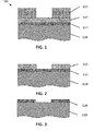
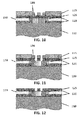
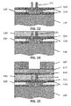
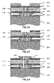
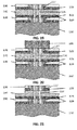
- FIG. 1 - 24 are schematic representations of various process steps in order, as used in embodiments of the present invention.
- FIGS. 1 to 24 illustrate an embodiment of a method according to the fourth aspect of the present invention.
- a field-effect transistor is produced.
- Each figure represents an intermediate stage of the method.
- FIG. 1 shows a semiconductor substrate (110) having a surface of Miller indices (1, 1, 1).
- Providing a semiconductor substrate having a surface of Miller indices (1,1,1) is advantageous because it allows, if the doped (>1e19 at/cm 3 ) III-V semiconductor material grown is a nanowire, for this nanowire to grow perpendicular to the substrate.
- An oxide layer (120) is provided on top of said substrate (110).
- This oxide layer (120) may for instance be a SiO 2 layer (120).
- a suitable thickness for this layer (120) is typically less than 20 nm and for instance 10 nm or less.
- a hard mask (115) is then provided on top of said oxide layer (120).
- a intermediate metal layer (not shown, e.g. 10 nm TiN) can be present between the oxide layer (120) and the hard mask (115).
- This hard mask (115) can for instance be a multilayer structure (not represented) such as a 70 nm amorphous carbon film (APF TM ), covered by a 20 nm SiOC layer.
- APF TM a patterned photoresist
- the pattern of the photoresist (105) is transferred to the hard mask (115). If the hard mask (115) was the multilayer described above, this pattern can be transferred by etching the SiOC through the patterned photoresist (105), followed by etching the amorphous carbon film thereby also consuming and therefore removing the photoresist (105) and then removing the remaining SiOC by wet (HF) or dry etch, followed by etching the TiN layer, and removing the amorphous carbon film by ashing.
- HF wet
- dry etch wet
- the pattern of the hard mask (115) is transferred to the oxide layer (120), thereby forming an oxide template (120) and exposing a portion of the semiconductor substrate (110).
- the exposed portion is not crucial and may for instance have an elliptic or a rounded square shape.
- the etching of the oxide layer (120) is preferably performed by a wet etching step for reasons detailed hereafter.
- this transfer can be performed by wet etching the SiO 2 layer (120) with diluted HF by using the patterned TiN layer as a mask.
- the use of such a wet etching permits to have a better selectivity toward the SiO 2 and therefore to spare the semiconductor substrate (e.g. a Si substrate) (110).
- the resulting undamaged substrate (110) surface is such as to promote the growth of a structure (125) of high crystalline quality on top of which high quality nanowires (126) will be grown in a subsequent step.
- the rest of the TiN is then etched.
- a structure (125) made of a doped (>1e19 at/cm 3 ) III-V semiconductor material is grown on said portion of the semiconductor substrate (110).
- This structure (125) will form the source (or drain) of the transistor and is preferably a nanowire (125).
- the structure represented in FIGs. 4-24 is not depicted as a nanowire (125) but as a more general structure (125) which height and/or aspect ratio is such as to provide a top surface having a threading dislocation defect density lower than 10 6 defects/cm 2 .
- This structure (125) is preferably a nanowire (125). When this structure (125) is a nanowire (125), the thickness of this nanowire (125) can for instance be in the range 20-30 nm.
- the base (128) i.e. the bottom layer of the structure (125) which is at the interface with the substrate 110 of this structure (125) is far from being defect-free due to lattice and/or material mismatch between the material of the substrate (110) and the III-V material of the structure (125).
- the base of the structure e.g. a nanowire
- the top of the structure (125) however has less than 10 6 threading dislocations/cm 2 because the structure (125) (preferably a nanowire) is grown to a sufficient height, permitting the tensions due to the lattice and/or material mismatch to relax.
- the top of the nanowire (125) will serve as the first surface on which one or more nanowires (126) of smaller cross sections (e.g. 10 nm diameter) will be grown.
- a barrier layer (130) is provided on the first surface.
- This barrier layer (130) can for instance be a Si 3 N 4 layer (130). It is then planarized via chemical mechanical planarization until the first surface becomes exposed and is made planar.
- steps analog to the steps performed in FIG. 1 are performed: an oxide layer (120) is provided on the structure (125) and the barrier layer (130). A hard mask (115) is then provided on the oxide layer (120). Then, a patterned photoresist (105) is provided on the hard mask (115).
- steps analog to the steps performed in FIG. 2 are performed: the pattern of the photoresist (105) is transferred to the hard mask (115), thereby exposing a portion of the oxide layer (120).
- a layer (135) of block-copolymer is provided on said portion of the oxide layer (120), said block-copolymer being formed of at least two block types, wherein one of said block types is suitable for forming vertical structures spanning the thickness of the layer (135) upon annealing.
- This block-copolymer can be for instance a PS-b-PMMA block co-polymer.
- the vertical structures (137) are typically cylinders of small diameters. For instance, cylinders of 15 nm diameter could be achieved with a PS-b-PMMA block co-polymer (with a pitch of 37 nm). Diameters of less than 15 nm can however be achieved with high-chi block-copolymers.
- the size of the vertical structures (137) can be controlled by varying the characteristics (e.g. the molecular weight) of the block-copolymer.
- the block-copolymer layer (135) is annealed, thereby creating the vertical structures (137) (in the case of a PS-PMMA block co-polymer, these vertical structures are made from the PMMA blocks (137) which are phase separated from the PS blocks (136)).
- these vertical structures are removed by wet etching, thereby forming a hole pattern in a PS layer where the block-copolymer layer was previously present.
- the hole pattern is transferred to the oxide layer (120) thereby exposing part of the first surface (129). This can be performed by etching, for instance wet etching.
- the PS blocks (136) are removed and then the hard mask (115) is removed (e.g. by a wet process), thereby exposing part of the first surface (129).
- the exposed part is composed of one or more holes of small dimensions (e.g. 30 nm diameter).
- undoped ( ⁇ 1e17 at/cm 3 ) III-V nanowires (126) are grown on said part of the first surface.
- the lattice mismatch between the first surface and the undoped ( ⁇ 1e17 at/cm 3 ) III-V nanowires (126) is minimal or not existing.
- the undoped ( ⁇ 1e17 at/cm 3 ) III-V nanowires (126) will serve as channels for the transistor.
- an oxide e.g. SiO 2
- a chemical mechanical planarization is performed to planarize until the top of the undoped ( ⁇ 1e17 at/cm 3 ) nanowires are exposed (126).
- steps analog to the steps performed in FIG. 1 or 6 are performed: an oxide layer (120) is provided on top of the undoped ( ⁇ 1e17 at/cm 3 ) nanowires (126) (and on top of oxide (140)) and a hard mask (115) is provided on top of said oxide layer (120). Finally, a patterned photoresist (105) is provided on top of the hard mask (115).
- steps analog to the steps performed in FIG. 2 or 7 are performed: the pattern of the photoresist (105) is transferred to the hard mask (115).
- the pattern of the hard mask (115) is transferred to the oxide layer (120), thereby forming an oxide template (120) and exposing the top of the undoped ( ⁇ 1e17 at/cm 3 ) nanowires (126) (as well as exposing a portion of the oxide (140)).
- a second structure (127) made of a doped (>1e19 at/cm 3 ) III-V semiconductor material is grown on said portion.
- the base of the second structure (127) tends to expand beyond the area defined by the top of the undoped nanowires (126) and the exposed portion of the oxide (140) (e.g. by 12%) to form a hexagonal base shape.
- This second structure (127) will form the drain (or source) of the transistor and is preferably a nanowire (127).
- a barrier layer (130) is provided on the second structure (127).
- This barrier layer (130) can for instance be a Si 3 N 4 layer. It is then planarized until the top of the second structure (127) becomes exposed and is planarized.
- an antireflective layer (not shown) is optionally provided on the second structure (127) and the barrier layer (130).
- a photoresist (105) is then provided on the antireflective layer (if present) or directly on part of the barrier layer (130) and on the second structure (127). If an antireflective layer was present, the photoresist can then be used to plasma etch part of the antireflective layer.
- a partial etching into the oxide layer (140) e.g. SiO 2 layer
- the antireflective coating is plasma etched, then the photoresist (105) is removed by ashing.
- a wet etch is performed in diluted HF to remove the rest of the oxide layer (140) and to remove the upper oxide material (120). This removal is selective toward the oxide (120) (e.g. SiO 2 ) and does not remove the barrier layer (130) (e.g. Si 3 N 4 ).
- a dielectric layer (145) is conformally deposited by ALD.
- a SiO 2 layer (145) is conformally deposited by ALD, followed by a high-K (145) deposition, also by ALD.
- a SiO 2 layer (145) or only a High-K layer (145) could be deposited.
- Metalization with TiN is performed thereby generating a gate metal coating (150) on the undoped ( ⁇ 1e17 at/cm 3 ) nanowires (126), followed by a chemical mechanical planarization.
Landscapes
- Engineering & Computer Science (AREA)
- Chemical & Material Sciences (AREA)
- Nanotechnology (AREA)
- Physics & Mathematics (AREA)
- Crystallography & Structural Chemistry (AREA)
- Condensed Matter Physics & Semiconductors (AREA)
- General Physics & Mathematics (AREA)
- Manufacturing & Machinery (AREA)
- Mathematical Physics (AREA)
- Theoretical Computer Science (AREA)
- Thin Film Transistor (AREA)
- Materials Engineering (AREA)
Abstract
Description
- The invention relates to the field of vertical nanowire semiconductor structures. More specifically it relates to a field-effect transistor (FET) based on one or more vertical nanowire channels and to methods to make and implement the same.
- In the context of CMOS scaling, it is established that below 7-nm CMOS generation, ie. sub N7, the standard planar/FinFET architecture need to switch to a vertical type of integration in order to continue scaling. Furthermore, electrostatic control needs to be improved. The best solution is to develop an architecture based on gate-all-around (GAA) vertical nanowires. Furthermore, in order to boost the drive current performances of the device, the use of a high mobility channel such as a III-V based channel is required.
- Based on the scaling predictions for N5 CMOS generation, the channel diameter should be smaller than 10 nm and more than one channel will need to be used in the device to increase drive current capabilities. Also, the channels will need to be as defect-free as possible in order to assure good electrical performances. Another problem of the vertical architecture is the source/drain regions for contacts that need to be highly doped (n-type or p-type), preferably in-situ, whilst limiting dopant diffusion in the channel which would degrade the carrier mobility. These issues represent key engineering challenges.
-
US Patent application 2013/0240983A1 discloses a process for fabricating a field-effect transistor device implemented on a network of vertical nanowires, including a plurality of elementary transistors, each elementary transistor comprising a source electrode and a drain electrode each positioned at one end of a vertical nanowire and connected by a channel, with a gate electrode surrounding each vertical nanowire.US Patent application 2013/0240983A1 discloses that these nanowires may be made from a group IV or group III-V materials and that these nanowires may be made preferably top-down (e.g. via etching). Alternatively, they may be made bottom-up (e.g. growth). It does not disclose a way to grow nanowires and therefore do not address the problem of how to grow nanowire-based channels with high crystalline quality. As having a low defect density vertical nanowire is important for device performance (e.g. for nanowire-based channels of FETs), there is still a need in the art for reducing the amount of defects in vertical nanowires and for methods to obtain the same. - It is an object of the present invention to provide vertical semiconductor nanowires having a low defect density in the channel of the device.
- It is another object of the present invention to provide methods to obtain the same.
- In a first aspect, the present invention relates to a semiconductor structure comprising a first surface and at least one nanowire, the at least one nanowire forming an angle with said first surface (and preferably being perpendicular to said first surface), wherein the first surface has a low density of threading dislocations and is made of a doped (>1e19 at/cm3) semiconductor material, wherein the at least one nanowire is made of an undoped (<1e17 at/cm3) semiconductor material having a lattice mismatch with the material of the first surface of from 0% to 1%, and wherein the doped (>1e19 at/cm3) semiconductor material and the undoped (<1e17 at/cm3) semiconductor material have each an electron mobility of at least 2000 cm2/(V.S) and/or a hole mobility of at least 500 cm2/(V.S). The at least one nanowire is abutting said first surface. One preferred way to obtain de facto a sufficiently low density of threading dislocations (and of crystal defects in general) in the first surface is to provide the first surface by growing a nanowire having a cross section larger than the cross section of the at least one nanowire. The top surface of this wider nanowire is in that embodiment the "first surface". This embodiment as well as alternatives are detailed in a later section of the present description.
- The invention originates from the realization by the inventors that the lattice mismatch between the ubiquitous Si substrate and the high mobility III-V material typically used for the channel of vertical FETs (such as GaAs (4% mismatch), In0.5Ga0.5As (8% mismatch), InAs (12% mismatch), GaSb (12% mismatch), In0.5Ga0.5Sb (16% mismatch) and InSb (20% mismatch)) generates high defect density in the channel that negatively impact the electrical performance of the device.
- In a second aspect, the present invention relates to a transistor comprising a semiconductor structure according to the first aspect.
- In a third aspect, the present invention relates to a device comprising a transistor according to the second aspect.
- In a fourth aspect, the present invention relates to a method for forming a semiconductor structure, said method comprising the steps of:
- Providing a first surface made of a doped (>1e19 at/cm3) semiconductor material and having a low density of threading dislocations (e.g. of less than 106/cm2), and
- Growing at least one nanowire on said first surface and at an angle thereto, said at least one nanowire being made of undoped (<1e17 at/cm3) semiconductor material having a lattice mismatch with the material of the first surface of from 0% to 1% and wherein the doped (>1e19 at/cm3) semiconductor material and the undoped (<1e17 at/cm3) semiconductor material have each an electron mobility of at least 2000 cm2/(V.S) and/or a hole mobility of at least 500 cm2/(V.S).
- It is an advantage of embodiments of the present invention that good group III-V-based vertical gate-all-around field-effect transistors comprising at least one defect-poor nanowire of high crystalline quality as the channel can be obtained.
- It is an advantage of embodiments of the present invention that the electrostatic control in the channel of the transistor is good, thereby leading to low leakage current density.
- It is an advantage of embodiments of the present invention that it may reduce the area needed by the transistor on a wafer (due to the vertical architecture), thereby improving the density in electronic components.
- It is an advantage of embodiments of methods of the fourth aspect of present invention that they can be CMOS compatible.
- The above objective is accomplished by a method and device according to the present invention.
- Particular and preferred aspects of the invention are set out in the accompanying independent and dependent claims. Features from the dependent claims may be combined with features of the independent claims and with features of other dependent claims as appropriate and not merely as explicitly set out in the claims.
- These and other aspects of the invention will be exposed from and elucidated with reference to the embodiment(s) described hereinafter.
- As used herein and unless provided otherwise, the term "nanowire" relates to a nanostructure having the shape of a rod, an aspect ratio of at least 2, preferably at least 3 and more preferably at least 5, and a width of at most 100 nm.
- A "lattice mismatch" (f) of a material A with a material B is calculated with the formula f=Δα/α, wherein Δα is the lattice parameter of material A minus the lattice parameter of material B, and wherein a is the lattice parameter of material B.
- A "threading dislocation" is a crystallographic defect, or irregularity, within a first crystalline structure, which is typically formed when said first crystalline structure is grown on a second mismatched crystalline structure. Growing a first crystalline structure on a second crystalline structure typically leads to the appearance of misfit dislocations to accommodate the lattice parameter difference at the substrate/layer interface. These misfits propagate as a threading dislocation in the above first crystalline structure.
- The presence and density of such threading dislocations can be measured by X-ray diffraction (XRD) or by Transmission Electrons Microscopy (TEM).
- As used herein and unless provided otherwise, the term "III-V" when characterizing a material, refers to a material made of compounds consisting of at least one group-III (IUPAC group 13) element and at least one group-V element (IUPAC group 15). This includes binary compounds but also higher order compounds such as ternary compounds. Examples include but are not limited to GaAs, InxGa1-xAs, InAs, GaSb, InxGa1-xSb, and InSb. Binary compounds are preferred because their stoechiometry is easier to control.
- A first aspect of the present invention relates to a semiconductor structure. This semiconductor structure is particularly useful in the fabrication of FETs but also in the fabrication of other devices in other fields such as sensors, NEMS, solar cells,...
- In embodiments, the semiconductor structure may be a FET or an intermediated structure in the fabrication of an FET. The semiconductor structure comprises a first surface and at least one nanowire abutting thereto. The at least one nanowire can consist in a set of from 1 up to 20 nanowires. In embodiments, each of the at least one nanowire may have a length of from 2 nm to 100 nm. Typically, at least 50%, preferably at least 70% and more preferably at least 90% of all the at least one nanowires have the same length. Most preferably, all of the at least one nanowires have the same length. The shape of the cross-section of each of the at least one nanowire is typically and preferably hexagonal. A hexagonal cross-section is typically indicative of a less defective crystalline structure than a non-hexagonal cross section. Each of the at least one nanowire is at an angle with the first surface and is preferably perpendicular thereto. Each of the at least one nanowire has one of its extremity abutting the first surface. The provided first surface has a low density of threading dislocations. In an embodiment, the first surface has at most 106 threading dislocation/cm2. In another embodiment, the first surface is substantially free of threading dislocations. The provided first surface also typically has a low density of stacking faults and twin boundaries. In an embodiment, the first surface has at most 106 stacking faults and twin boundaries combined/cm2. Methods to obtain such defect-poor first surfaces are provided in the fourth aspect of the present invention. A stacking fault is a change in the stacking sequence over a few atomic spacings. A twin boundary is a change over many atomic spacings. These stacking faults and twin boundaries defects are parallel to the (1, 1, 1) orientation of a crystalline material. During the growth of the structure comprising the first surface, the number of defects gradually but relatively rapidly decreases with the increasing height of the structure. This is due to the accompanying relaxation of the crystal lattice for each new crystal layer grown on top of the preceding one. This way, the number of stacking faults and twin boundaries decreases to very low level once a sufficient height, and therefore a sufficient aspect ratio, has been achieved for the structure. In embodiment, a sufficient aspect ratio is 2 or more, preferably 5 or more, more preferably 10 or more, most preferably 20 or more. An advantage of using a (1, 1, 1) first surface is that it permits the growth of the at least one nanowire vertically thereon. Another advantage is that since the stacking faults and twin boundaries defects are parallel to the (1, 1, 1) orientation, a defect poor first surface is more easily and rapidly achieved.
- The first surface is made of a highly doped semiconductor material (above 1e19 at/cm3). The semiconductor material has an electron mobility of at least 2000 cm2/(V.s) and/or a hole mobility of at least 500 cm2/(V.S).Preferred semiconductor materials are groups III-V semiconductor materials. The first surface preferably has Miller indices (1, 1, 1).
- In an embodiment, the cross section of each of the at least one nanowire, averaged over the length of that nanowire, has a threading dislocation density of less than 106/cm2. In an embodiment, the cross section of each of the at least one nanowire, averaged over the length of that nanowire, has at most 106 stacking faults and twin boundaries combined/cm2. The at least one nanowire is made of an undoped semiconductor material (doping density <1e17 at/cm3) having a mobility of at least 2000 cm2/(V.s) and having a lattice mismatch with the material of the first surface of from 0% to 1%. Preferably, the lattice mismatch is from 0.0% to 0.5%. More preferably, it is from 0.0 to 0.2%. Most preferably, there is no lattice mismatch. One way to avoid lattice mismatch is to use the same semiconductor material for the doped (>1019 at/cm3) first surface and for the undoped (<1017 at/cm3) nanowire (e.g. for the channel). Preferred semiconductor materials are groups III-V semiconductor materials. Another way to avoid lattice mismatch is to adapt the composition of a III-V material in order to match the lattice parameters of the first surface. For instance a ternary III-V material can have its composition fine-tuned for that purpose. This approach is however less preferred than simply using the same semiconductor material for the first surface and the one or more nanowires. Low lattice mismatch is advantageous because it minimize strain in the nanowire and therefore strain-induced defects. The at least one nanowire may have a width of from 1 to 50 nm, preferably from 1 to 10 nm and a length of from 2 to 100 nm, preferably 5 to 50 nm, more preferably from 10 to 30 nm.
- In embodiments, said at least one nanowire may have a first cross section, and the first surface may be a first extremity of a nanowire having a second cross section, larger than said first cross section. The second cross-section is sufficient for supporting said at least one nanowire having a first cross section. This should be construed as allowing all the bases of the at least one nanowire having a first cross-section to fit in their entirety on the first surface.
- In embodiments, the second cross-section may be from 2 to 100 nm, preferably from 3 to 40 nm, more preferably from 4 to 30 nm.
- In embodiments, the length (or height) of the nanowire providing the first surface may be from 10 to 200 nm, preferably 15 to 80 nm.
- In this embodiment, since a nanowire is used to provide the first surface, the first surface will de facto have a sufficiently low density of defects (threading dislocations, stacking faults and twin boundaries) for the performance of the present invention. In particular, there is no need to measure the density of defects of that first surface. This is typically already the case for a first surface provided by a nanowire having an aspect ratio of 2 or more and a height (length) of 10 nm or more.
- As a non-limiting example, if said at least one nanowire is a set of seven nanowires having each a first cross-section having a width (or diameter) of 10 nm, the nanowire having a second cross-section could have a cross-section having a width of at least 30 nm to allow the seven bases to fit in their entirety on the first surface.
- In embodiments, said nanowire having a second cross section possess said first extremity and a second extremity and the second extremity is abutting a surface of a substrate.
- In embodiments, said surface of a substrate may have Miller indices (1,1,1). Using such a substrate surface is advantageous as it permits growing thereon a nanowire comprising said first surface sharing the same Miller indices (1, 1, 1), thereby permitting the growth of the at least one nanowire vertically on said first surface. In embodiments, the substrate is preferably a silicon or germanium substrate, most preferably a silicon substrate. One of the major advantages of the present invention is that it permits the use of the ubiquitous Si substrate despite its lattice mismatch with semiconductor materials having high electrons or holes mobilities such as III-V materials. Despite the use of Si as the substrate, embodiments of the present invention permit obtaining at least one nanowire that is defect-poor and that can be used as channels for an FET. Although starting from a III-V substrate is possible and remains within the broadest definition of the present invention, it is hardly compatible with CMOS processes. Various embodiments of the present invention show how to remain CMOS compatible by providing locally on a typical substrate (such as a Si substrate) a first doped (>1e19 at/cm3) III-V surface on which at least one III-V nanowire can be grown.
- In a preferred embodiment, the present invention may relate to a semiconductor structure comprising:
- at least one nanowire made of an undoped (<1e17 at/cm3) III-V material having a first cross-section, a base surface and a top surface,
- a nanowire made of a doped (>1e19 at/cm3) III-V material and having a second cross-section, a base surface and a first surface opposite to the base surface, whereby the second cross-section is larger than said first cross-section and sufficient for allowing the base surfaces of the at least one nanowire having a first cross-section to fit in their entirety on the top surface of the nanowire having a second cross-section,
- In any embodiments, the semiconductor structure may further comprise a second surface made of a doped (>1e19 at/cm3) III-V semiconductor material, wherein said at least one nanowire is sandwiched between said first surface and said second surface.
- In embodiments, said second surface may be an extremity of a nanowire having a cross section sufficient for allowing the cross section (and therefore the top surfaces) of the at least one nanowire having a first cross-section to fit in their entirety on the second surface.
- In a second aspect, the present invention relates to a field-effect transistor comprising a semiconductor structure according to the first aspect. In this second aspect, the at least one nanowire may comprise a channel or may form a corresponding number of channels of the field-effect transistor.
- The first surface may belong to a source (or a drain) of the transistor and the second surface may belong to a drain (or a source) of the transistor. The transistor typically comprises a gate electrode.
- A gate electrode may either i) comprise a layer of dielectric material embedding all of said at least one nanowire, and a layer of conducting material around said layer of dielectric material, or ii) comprise a number of layers of dielectric material, said number corresponding to the number of nanowires composing said "at least one nanowire", each of said layer surrounding one of said nanowires.
- A gate electrode may comprise:
- a layer of dielectric material surrounding a portion or the entirety of each of said at least one nanowire, and
- a layer of conductive material around (each of) said layer of dielectric material.
- Preferably, the layer of conducting material is unique for all of the at least one nanowire. The thickness of the layer of conducting material (in case i) )corresponds to the length of the gate of the transistor.
- In embodiments, contacts between the source and the gate and between the drain and the gate may be insulated.
- Typically, the field-effect transistor of the second aspect is implemented on at least one nanowire forming a corresponding number of channels sharing a same source and a same drain. The source is typically abutting at one end of the at least one nanowire and the drain is typically abutting at another end of the at least one nanowire, with the at least one nanowire forming the channel(s) connecting the source and the drain.
- The field-effect transistor may comprise a dielectric material so as to insulate the source and the drain to form the contacts between the source and gate and between the drain and gate.
- The conductive material forming the gate electrode can for instance be made from metal (e.g. TiN), silicide, amorphous silicon or polysilicon.
- The dielectric material may be selected from oxides of silicon (e.g. silicon dioxide) and high-K dielectrics such as oxides of Al, Zr, Hf, Gd or La.
- In a third aspect, the present invention relates to a device comprising a field-effect transistor according to the second aspect. In embodiments, the device may comprise a plurality of field-effect transistors according to the second aspect. Examples of such electronic devices are bio-sensors, chemo-sensors, volatile memory, non-volatile memory, CMOS inverter, multiplexers, and logic circuits.
- In a fourth aspect, the present invention relates to a method for forming a semiconductor structure, said method comprising the steps of:
- Providing a first surface made of a doped (>1e19 at/cm3) semiconductor material, said first surface having a low density of threading dislocations (e.g. less than 106 per cm2), and
- Growing at least one nanowire on said first surface and at an angle thereto, said at least one nanowire being made of undoped (<1e17 at/cm3) semiconductor material having a lattice mismatch with the material of the first surface of from 0% to 1% and wherein the doped (>1e19 at/cm3) semiconductor material and the undoped (<1e17 at/cm3) semiconductor material have each an electrons mobility of at least 2000 cm2/(V.S) and/or an holes mobility of at least 500 cm2/(V.S).
- In embodiments, the doped (>1e19 at/cm3) semiconductor material may be a doped (>1e19 at/cm3) III-V semiconductor material.
- In embodiments, the undoped (<1e17 at/cm3) semiconductor material may be a undoped (<1e17 at/cm3) III-V semiconductor material.
- In embodiments, the step of providing a first surface having a low density of threading dislocations (e.g. less than 106 threading dislocation defects/cm2) may comprise growing a semiconductor structure to a height sufficient for its top surface to have said low density of threading dislocations.
- Alternatively, a defect-poor first surface (e.g. having less than 106 threading dislocation defects/cm2, and/or having at most 106 stacking faults and twin boundaries combined/cm2) may be a full wafer of semiconductor material serving as the substrate, or it can be a portion of a full wafer that has been etched to any desirable dimension or that has been separated from the wafer and that is used as the substrate or that is attached (e.g. glued) on a substrate. Preferably however, said at least one nanowire may have a first cross-section, and the step of providing a first surface having a low amount of defects (e.g. having less than 106 threading dislocation defects/cm2) may comprise growing a nanowire having a cross-section larger than said first cross-section and sufficient for supporting said at least one nanowire having a first cross-section.
- In embodiments, providing a first defect-poor surface (e.g. having less than 106 threading dislocations/cm2) may comprise the following steps:
- Providing a substrate,
- Providing a patterned oxide layer on said substrate, thereby leaving exposed a portion of the substrate,
- Growing a doped (>1e19 at/cm3) semiconductor material on said portion, wherein said material is grown either
- ∘ to a height sufficient for the top surface of said material to have less than 106 threading dislocations/cm2, and/or
- ∘ to a height of at least 10 nm and sufficient for providing an aspect ratio of 2 to the grown doped semiconductor material (this correspond to growing on said portion a nanowire having a length of at least 10 nm said length being at least twice the width of this nanowire)
- In embodiments, providing a patterned oxide layer on said substrate may comprise the following steps:
- Providing an oxide layer on said substrate,
- Providing a patterned hard mask on said oxide layer, and
- Transferring the pattern of the hard mask to the oxide layer, thereby leaving exposed a portion of the substrate.
- In embodiments, providing a patterned hard mask may comprise the following steps:
- Providing a hard mask on said oxide layer,
- Providing a patterned photoresist on said hard mask, and
- Transferring the pattern of the photoresist to the hard mask.
- In embodiments, after the step of growing a doped (>1e19 at/cm3) semiconductor material on said portion, the method may further comprise the following steps aiming at planarizing said defect-poor first surface:
- Providing a barrier layer on said first surface (and in practice also typically on part of the patterned oxide layer), and
- Planarizing said barrier layer until said first surface is exposed and is itself planarized.
- In embodiments, after the step of growing a doped (>1e19 at/cm3) semiconductor material on said portion, and after planarization is performed, the method may further comprise the following steps:
- Providing a patterned protective layer on the first surface, wherein said pattern comprises holes having a width of from 1 to 20 nm and wherein said protective layer is made of a material that can be etched selectively with respect to the first surface. The holes are exposing portions of the first surface.
Figure 12 is an illustration of the end result of this embodiment where thetop layer 120 is the patterned protective layer. In practice, the patterned protective layer will be provided on the first surface but will also typically extend beyond that surface (seeFig. 12 where thetop layer 120 also extends on the barrier layer 130). The holes will typically have a length of from 1 to 20 nm. The width and the length of the holes are typically within 50% or one another and more typically equal. - In embodiments, providing a patterned protective layer on the first surface may comprise the following steps:
- Overlaying said first surface with a protective layer,
- Providing a patterned mask on said protective layer, wherein said pattern comprises holes of width of from 1 to 20 nm, and
- Etching said protective layer through said holes and selectively with respect to the first surface.
- The step of overlaying said first surface with a protective layer is illustrated for an embodiment in
Fig. 6 . In that figure, the protective layer bears number 120 (top). In practice, the patterned protective layer will be provided on the first surface but will also typically extend beyond that surface (seeFig. 6 where thetop layer 120 also extends on the barrier layer 130). In the step of providing a patterned mask, the holes are vertically aligned with portions of the first surface that will be exposed in the etching step. The end result of the step of providing a patterned mask on said protective layer is illustrated for an embodiment inFig. 10 where the patterned mask is made of polystyrene. The end result of the etching step is illustrated in an embodiment inFig. 11 . - In embodiments, providing a patterned mask on the protective layer may comprise the following steps:
- Providing a patterned hard mask on said protective layer, leaving portions of the protective layer exposed (this is illustrated for an embodiment in
Fig. 7 where the exposed portions are above the first surface so that a vertical projection of the exposed portions is comprised in the first surface), - Providing a layer of a block-copolymer on said portions, said block-copolymer being formed of at least two block types, wherein one of said block types is suitable for forming vertical structures spanning the thickness of the layer upon annealing (this is illustrated for an embodiment in
Fig. 8 ), - Annealing said block-copolymer, thereby generating said vertical structures (this is illustrated for an embodiment in
Fig. 9 ), and - Removing said vertical structures by etching (e.g. plasma etching or preferably wet etching), thereby forming a hole pattern in said block-copolymer, thereby forming the patterned mask (this is illustrated for an embodiment in
Fig. 10 ). - In the step of providing a patterned hard mask, the exposed portions are typically vertically aligned with portions of the first surface on which the one or more nanowire will be grown.
- The substrate may be as defined in any embodiment of the first aspect.
- The oxide layer is preferably SiO2 and preferably has a thickness equal to the height of the at least one nanowire. For instance, the thickness may be from 1 to 20 nm, preferably from 1 to 10 nm.
- The hard mask can be any material that can:
- be patterned and which pattern can be transferred into an oxide layer such as e.g. SiO2, and
- be remove easily (e.g. by plasma or wet etch).
- The hard mask is typically harder than the photoresist.
- The hard mask can for instance be a silicon oxycarbide (SiOC)/amorphous carbon stack, a spin-on-glass (SoG)/ spun on carbon (SoC) stack, a SiO2/Si3N4/SiO2 stack, or a Si3N4/amorphous silicon (a-Si) stack.
- The amorphous carbon can for instance be a PECVD ashable amorphous carbon film of the Advanced Patterning Film™ (APF™) type.
- The block-copolymer may be a polymer having two or more chemically different polymer blocks, for example a di-block, tri-block, star, comb or other polymer with controlled structure. The blocks may typically have different chemical properties, such as the degree of hydrophilicity or hydrophobicity. The blocks may typically be mutually immiscible, or only partially miscible, (at least) over a range of temperatures, e.g. to allow formation of separate micro-phase domains, thus enabling self-assembly. Self-assembly may be based on chemical differences between the different polymer blocks, e.g. a hydrophilicity/hydrophobicity imbalance. Such block-copolymers may be obtained by methods known in the art, for example by atom transfer radical polymerization, reversible addition fragmentation chain transfer polymerization, nitroxide-mediated polymerization, boron-mediated polymerization or catalytic chain transfer polymerization.
- Annealing relates to a process that allows self-assembly of structures by micro-phase separation in a block-copolymer material. This process may for instance comprise heating up the block-copolymer or contacting the block-copolymer with a solvent, or both. Typically, it consists in heating up the block-copolymer. Upon annealing, the chemically different polymer blocks undergo a microphase separation, which is driven by repulsion between the dissimilar polymer chains, such that homogenous domains in a periodic nanostructure are formed after annealing. For example, such periodic structures may comprise hexagonally packed cylinders. The type of structure which is formed is furthermore controllable by tuning the ratios of the different polymer block lengths.
- In embodiments, the block-copolymer may be a block-copolymer comprising at least two polymer components having mutually different etching resistances and forming a pattern structure by micro-phase separation of the at least two polymer components upon annealing. The block-copolymer may comprise at least two polymer components having mutually different etching resistances. For example, a polymeric composition consisting of two or more chemically different homopolymer blocks connected by covalent bonds at their chain ends may be coated onto the portion, e.g. by brushing, rolling, spraying, inkjet application or spin-coating. The polymeric composition may furthermore comprise additives, e.g. adhesives, adhesion promoters and/or solvents. For example, the block-copolymer may be formed from a di-block copolymer composition comprising two types of polymer chains covalently bonded to each other. For example, such di-block copolymer may comprise polystyrene-polyisobutene, polystyrene-isoprene, polydimethylsiloxane-polyisobutene, polystyrene-polyethylene oxide, polystyrene-polypropylene oxide, polyethyleneoxide-poly(cyanobiphenyloxy)hexyl methacrylate, polystyrene-polymethacrylic acid, polyethylene oxide-polyvinylpyridine, polystyrene-polyvinylpyridine, or polyisoprene-polyhydroxystyrene. Preferably, such di-block copolymer may comprise polystyrene (PS) chains covalently bonded to polymethyl methacrylate (PMMA) chains, in which the polystyrene and PMMA have an advantageous etch resistance ratio for dry etching with argon plasma. Alternatively, the self-organizing block-copolymer layer may be formed from a tri-block copolymer composition, for example in which two types of polymer chains A,B are bonded in an A-B-A form or in which three types of polymer chains A,B,C are bonded in an A-B-C form. In an embodiment, one of said polymer component (e.g. said second polymer component) may be polystyrene.
- In an embodiment, one of said polymer component (e.g. said first polymer component) may be PMMA.
- The self-organizing block-copolymer layer furthermore has a copolymer pattern structure which can be formed by micro-phase separation of the at least two polymer components upon annealing. For example, the block-copolymer coated onto the portion may be annealed, e.g. at a temperature higher than the glass-transition or melting temperature, during which the components of the block-copolymer may self-assemble into structured domains, thus forming the copolymer pattern structure. For example, thermal annealing may be used at a temperature above the lowest value of the glass transition or melting temperature of at least one polymeric component of the composition. Annealing time may be selected to allow self-assembly, and may be in the range of 0.01 hours to 300 hours, preferably between 0.1 hours and 24 hours. Prior to the annealing, a pre-bake may be performed in order to remove any residual solvent after block-copolymer deposition (e.g. by spin-casting). In the case of a PS-PMMA block co-polymer, this pre-bake may for instance be performed at a temperature within the range 70°C-130°C (e.g. 100°C) for 30-120 seconds (e.g. 60 seconds). It is advantageous to choose pre-bake conditions that lead to a uniform film across the substrate. In the case of a PS-PMMA block co-polymer, the actual annealing of the block-copolymer may for instance be performed at a temperature of from 200°C-300°C (e.g. 250°C) for a time span of from 100 to 500 seconds (e.g. 300 seconds) in an oven under inert (e.g. N2) atmosphere.
- By selecting an appropriate total chain length and molecular weight of each block in the block-copolymer, e.g. selecting an appropriate Flory Huggins parameter, as known in the art, the morphology of this copolymer pattern structure may be tuned in order to create e.g. cylinders in the block-copolymer layer. The molecular weight of the block-copolymer may be, for example, selected such that the end-to-end distance of the blocks is commensurate with the smallest feature of the intended pattern. Preferred molecular weights may range, for example, from 200 to 1000000 g/mol, e.g. from 2000 to 100000 g/mol.
- The protective layer is preferably an oxide layer. In embodiments, this oxide layer can be a silicon oxide layer such as SiO2. SiO2 is advantageous because it can be etched very selectively compared to III-V materials. The etching method used therefore is typically a wet etch.
- The step of providing a patterned mask on said protective layer can for instance comprise:
- providing a hard mask on said protective layer,
- providing a patterned photoresist on said hard mask, and
- transferring the pattern of the photoresist to the hard mask, thereby exposing a portion of the protective layer.
- The step of growing undoped (<1e17 at/cm3) semiconductor nanowires may be performed by epitaxial growth, i.e. by exposing the first surface to gaseous or liquid precursors of semiconductor nanowires (e.g. of III-V semiconductor nanowires), thereby using the first surface as a seed for growing the nanowire.
- In order for the length of the nanowires to be made uniform and for their top surface to be made planar, an oxide (e.g. SiO2) may be deposited to cover (and embed) the undoped (<1e17 at/cm3) nanowires, then chemical mechanical planarization may be performed to planarize the top of the undoped (<1e17 at/cm3) nanowires (126).
- In embodiments, the method may further comprise providing a second surface made of a doped (>1e19 at/cm3) III-V semiconductor material, so that said at least one nanowire is sandwiched between said first surface and said second surface.
- In embodiments, providing a second surface may comprise the following steps:
- providing an oxide to cover (entirely) the at least one undoped (<1e17 at/cm3) semiconductor nanowire,
- planarizing the top of the at least one nanowire,
- providing a patterned oxide layer (at least) on top of the at least one nanowire in such a way as to at least leave the top of the at least one nanowire exposed, and
- growing a doped (>1e19 at/cm3) semiconductor material at least on said exposed tops parts, thereby providing said second surface.
- The second surface is abutting the top of the at least one nanowire.
- In embodiments, providing a patterned oxide layer on the first surface may comprise the following steps:
- providing an oxide layer on top of the at least one nanowires,
- providing a patterned hard mask on said oxide layer,
- transferring the pattern of the hard mask to said oxide layer.
- In embodiments, providing a patterned hard mask on said oxide layer may comprise the following steps:
- providing a hard mask on said oxide layer,
- providing a patterned photoresist on said hard mask, and
- transferring the pattern of the photoresist to the hard mask.
- In embodiments, the doped (>1e19 at/cm3) semiconductor material grown on said exposed parts may be as described for the doped (>1e19 at/cm3) semiconductor used to obtain the first surface. The step of growing the undoped (<1e17 at/cm3) semiconductor may also be as described for the growing of the doped (>1e19 at/cm3) semiconductor used to obtain the first surface.
- Once the second surface has been provided, the resulting structure comprises a first surface, at least one nanowire and a second surface. This structure can be an intermediate in the construction of an FET wherein the at least one nanowire may be at least one channel, the first surface belongs to a source (or a drain) and the second surface belongs to a drain (or a source). In order to complete the FET, the following steps may be performed:
- providing a barrier layer on the doped (>1e19 at/cm3) semiconductor material providing said second surface,
- planarizing the barrier layer until the top of the doped (>1e19 at/cm3) semiconductor material becomes exposed and is planarized,
- optionally providing an antireflective coating layer on the doped (>1e19 at/cm3) semiconductor material and the barrier layer,
- providing a photoresist on the antireflective layer (if present) or directly on part of the barrier layer and on the doped (>1e19 at/cm3) semiconductor material,
- etching the antireflective coating if present,
- etching partially into the oxide layer,
- removing the photoresist,
- selectively removing the remaining oxide material without removing the barrier layer,
- depositing conformally a dielectric layer on the at least one nanowire, and
- providing a metal coating on the dielectric layer
- In general, any element mentioned in the fourth aspect may be as described for the same element mentioned in the first aspect.
-
FIG. 1 - 24 are schematic representations of various process steps in order, as used in embodiments of the present invention. - The drawings are only schematic and are non-limiting. In the drawings, the size of some of the elements may be exaggerated and not drawn on scale for illustrative purposes. Any reference signs in the claims shall not be construed as limiting the scope. In the different drawings, the same reference signs refer to the same or analogous elements.
- The present invention will be described with respect to particular embodiments and with reference to certain drawings but the invention is not limited thereto but only by the claims. The drawings described are only schematic and are non-limiting. In the drawings, the size of some of the elements may be exaggerated and not drawn on scale for illustrative purposes. The dimensions and the relative dimensions do not correspond to actual reductions to practice of the invention.
- Furthermore, the terms first, second and the like in the description and in the claims, are used for distinguishing between similar elements and not necessarily for describing a sequence, either temporally, spatially, in ranking or in any other manner. It is to be understood that the terms so used are interchangeable under appropriate circumstances and that the embodiments of the invention described herein are capable of operation in other sequences than described or illustrated herein.
- Moreover, the terms top, under and the like in the description and the claims are used for descriptive purposes and not necessarily for describing relative positions. It is to be understood that the terms so used are interchangeable under appropriate circumstances and that the embodiments of the invention described herein are capable of operation in other orientations than described or illustrated herein.
- It is to be noticed that the term "comprising", used in the claims, should not be interpreted as being restricted to the means listed thereafter; it does not exclude other elements or steps. It is thus to be interpreted as specifying the presence of the stated features, integers, steps or components as referred to, but does not preclude the presence or addition of one or more other features, integers, steps or components, or groups thereof. Thus, the scope of the expression "a device comprising means A and B" should not be limited to devices consisting only of components A and B. It means that with respect to the present invention, the only relevant components of the device are A and B.
- Reference throughout this specification to "one embodiment" or "an embodiment" means that a particular feature, structure or characteristic described in connection with the embodiment is included in at least one embodiment of the present invention. Thus, appearances of the phrases "in one embodiment" or "in an embodiment" in various places throughout this specification are not necessarily all referring to the same embodiment, but may. Furthermore, the particular features, structures or characteristics may be combined in any suitable manner, as would be exposed to one of ordinary skill in the art from this disclosure, in one or more embodiments.
- Similarly it should be appreciated that in the description of exemplary embodiments of the invention, various features of the invention are sometimes grouped together in a single embodiment, figure, or description thereof for the purpose of streamlining the disclosure and aiding in the understanding of one or more of the various inventive aspects. This method of disclosure, however, is not to be interpreted as reflecting an intention that the claimed invention requires more features than are expressly recited in each claim. Rather, as the following claims reflect, inventive aspects lie in less than all features of a single foregoing disclosed embodiment. Thus, the claims following the detailed description are hereby expressly incorporated into this detailed description, with each claim standing on its own as a separate embodiment of this invention.
- Furthermore, while some embodiments described herein include some but not other features included in other embodiments, combinations of features of different embodiments are meant to be within the scope of the invention, and form different embodiments, as would be understood by those in the art. For example, in the following claims, any of the claimed embodiments can be used in any combination.
- In the description provided herein, numerous specific details are set forth. However, it is understood that embodiments of the invention may be practiced without these specific details. In other instances, well-known methods, structures and techniques have not been shown in detail in order not to obscure an understanding of this description.
-
Figures 1 to 24 illustrate an embodiment of a method according to the fourth aspect of the present invention. In this embodiment, a field-effect transistor is produced. Each figure represents an intermediate stage of the method. -
FIG. 1 shows a semiconductor substrate (110) having a surface of Miller indices (1, 1, 1). Providing a semiconductor substrate having a surface of Miller indices (1,1,1) is advantageous because it allows, if the doped (>1e19 at/cm3) III-V semiconductor material grown is a nanowire, for this nanowire to grow perpendicular to the substrate. - An oxide layer (120) is provided on top of said substrate (110). This oxide layer (120) may for instance be a SiO2 layer (120). A suitable thickness for this layer (120) is typically less than 20 nm and for instance 10 nm or less. A hard mask (115) is then provided on top of said oxide layer (120). A intermediate metal layer (not shown, e.g. 10 nm TiN) can be present between the oxide layer (120) and the hard mask (115). This hard mask (115) can for instance be a multilayer structure (not represented) such as a 70 nm amorphous carbon film (APF™), covered by a 20 nm SiOC layer. Finally, a patterned photoresist (105) is provided on top of the hard mask (115).
- In
FIG. 2 , the pattern of the photoresist (105) is transferred to the hard mask (115). If the hard mask (115) was the multilayer described above, this pattern can be transferred by etching the SiOC through the patterned photoresist (105), followed by etching the amorphous carbon film thereby also consuming and therefore removing the photoresist (105) and then removing the remaining SiOC by wet (HF) or dry etch, followed by etching the TiN layer, and removing the amorphous carbon film by ashing. - In
FIG. 3 , the pattern of the hard mask (115) is transferred to the oxide layer (120), thereby forming an oxide template (120) and exposing a portion of the semiconductor substrate (110). The exposed portion is not crucial and may for instance have an elliptic or a rounded square shape. The etching of the oxide layer (120) is preferably performed by a wet etching step for reasons detailed hereafter. In the case of an SiO2 oxide layer (120) and of the multilayer hard mask (115) exemplified above, this transfer can be performed by wet etching the SiO2 layer (120) with diluted HF by using the patterned TiN layer as a mask. The use of such a wet etching permits to have a better selectivity toward the SiO2 and therefore to spare the semiconductor substrate (e.g. a Si substrate) (110). The resulting undamaged substrate (110) surface is such as to promote the growth of a structure (125) of high crystalline quality on top of which high quality nanowires (126) will be grown in a subsequent step. The rest of the TiN is then etched. - In
FIG. 4 , a structure (125) made of a doped (>1e19 at/cm3) III-V semiconductor material is grown on said portion of the semiconductor substrate (110). This structure (125) will form the source (or drain) of the transistor and is preferably a nanowire (125). The structure represented inFIGs. 4-24 however is not depicted as a nanowire (125) but as a more general structure (125) which height and/or aspect ratio is such as to provide a top surface having a threading dislocation defect density lower than 106 defects/cm2. This structure (125) is preferably a nanowire (125). When this structure (125) is a nanowire (125), the thickness of this nanowire (125) can for instance be in the range 20-30 nm. The base (128) (i.e. the bottom layer of the structure (125) which is at the interface with the substrate 110) of this structure (125) is far from being defect-free due to lattice and/or material mismatch between the material of the substrate (110) and the III-V material of the structure (125). Also, the base of the structure (e.g. a nanowire) (125) tend to expand beyond the actual area of said portion of the semiconductor substrate (110) (e.g. by 12%) to form a hexagonal base shape. The top of the structure (125) however has less than 106 threading dislocations/cm2 because the structure (125) (preferably a nanowire) is grown to a sufficient height, permitting the tensions due to the lattice and/or material mismatch to relax. The top of the nanowire (125) will serve as the first surface on which one or more nanowires (126) of smaller cross sections (e.g. 10 nm diameter) will be grown. - In
FIG. 5 , a barrier layer (130) is provided on the first surface. This barrier layer (130) can for instance be a Si3N4 layer (130). It is then planarized via chemical mechanical planarization until the first surface becomes exposed and is made planar. - In
FIG. 6 , steps analog to the steps performed inFIG. 1 are performed: an oxide layer (120) is provided on the structure (125) and the barrier layer (130). A hard mask (115) is then provided on the oxide layer (120). Then, a patterned photoresist (105) is provided on the hard mask (115). - In
FIG. 7 , steps analog to the steps performed inFIG. 2 are performed: the pattern of the photoresist (105) is transferred to the hard mask (115), thereby exposing a portion of the oxide layer (120). - In
FIG. 8 , a layer (135) of block-copolymer is provided on said portion of the oxide layer (120), said block-copolymer being formed of at least two block types, wherein one of said block types is suitable for forming vertical structures spanning the thickness of the layer (135) upon annealing. This block-copolymer can be for instance a PS-b-PMMA block co-polymer. The vertical structures (137) are typically cylinders of small diameters. For instance, cylinders of 15 nm diameter could be achieved with a PS-b-PMMA block co-polymer (with a pitch of 37 nm). Diameters of less than 15 nm can however be achieved with high-chi block-copolymers. The size of the vertical structures (137) can be controlled by varying the characteristics (e.g. the molecular weight) of the block-copolymer. - In
FIG. 9 , the block-copolymer layer (135) is annealed, thereby creating the vertical structures (137) (in the case of a PS-PMMA block co-polymer, these vertical structures are made from the PMMA blocks (137) which are phase separated from the PS blocks (136)). - In
FIG. 10 , these vertical structures (e.g. PMMA) are removed by wet etching, thereby forming a hole pattern in a PS layer where the block-copolymer layer was previously present. - In
FIG. 11 , the hole pattern is transferred to the oxide layer (120) thereby exposing part of the first surface (129). This can be performed by etching, for instance wet etching. - In
FIG. 12 , the PS blocks (136) are removed and then the hard mask (115) is removed (e.g. by a wet process), thereby exposing part of the first surface (129). The exposed part is composed of one or more holes of small dimensions (e.g. 30 nm diameter). - In
FIG. 13 , undoped (<1e17 at/cm3) III-V nanowires (126) are grown on said part of the first surface. The lattice mismatch between the first surface and the undoped (<1e17 at/cm3) III-V nanowires (126) is minimal or not existing. The undoped (<1e17 at/cm3) III-V nanowires (126) will serve as channels for the transistor. - In
FIG. 14 , an oxide (e.g. SiO2) (140) is deposited to cover (and embed) the undoped (<1e17 at/cm3) nanowires (126), then chemical mechanical planarization is performed to planarize until the top of the undoped (<1e17 at/cm3) nanowires are exposed (126). - In
FIG. 15 , steps analog to the steps performed inFIG. 1 or6 are performed: an oxide layer (120) is provided on top of the undoped (<1e17 at/cm3) nanowires (126) (and on top of oxide (140)) and a hard mask (115) is provided on top of said oxide layer (120). Finally, a patterned photoresist (105) is provided on top of the hard mask (115). - In
FIG. 16 , steps analog to the steps performed inFIG. 2 or7 are performed: the pattern of the photoresist (105) is transferred to the hard mask (115). - In
FIG. 17 , the pattern of the hard mask (115) is transferred to the oxide layer (120), thereby forming an oxide template (120) and exposing the top of the undoped (<1e17 at/cm3) nanowires (126) (as well as exposing a portion of the oxide (140)). - In
FIG. 18 , a second structure (127) made of a doped (>1e19 at/cm3) III-V semiconductor material is grown on said portion. Similarly toFig. 4 , the base of the second structure (127) tends to expand beyond the area defined by the top of the undoped nanowires (126) and the exposed portion of the oxide (140) (e.g. by 12%) to form a hexagonal base shape. This second structure (127) will form the drain (or source) of the transistor and is preferably a nanowire (127). - In
FIG. 19 , a barrier layer (130) is provided on the second structure (127). This barrier layer (130) can for instance be a Si3N4 layer. It is then planarized until the top of the second structure (127) becomes exposed and is planarized. - In
Fig. 20 , an antireflective layer (not shown) is optionally provided on the second structure (127) and the barrier layer (130). A photoresist (105) is then provided on the antireflective layer (if present) or directly on part of the barrier layer (130) and on the second structure (127). If an antireflective layer was present, the photoresist can then be used to plasma etch part of the antireflective layer. - In
FIG. 21 , a partial etching into the oxide layer (140) (e.g. SiO2 layer) is performed, then, if present, the antireflective coating is plasma etched, then the photoresist (105) is removed by ashing. - In
FIG. 22 , a wet etch is performed in diluted HF to remove the rest of the oxide layer (140) and to remove the upper oxide material (120). This removal is selective toward the oxide (120) (e.g. SiO2) and does not remove the barrier layer (130) (e.g. Si3N4). - In
FIG. 23 , a dielectric layer (145) is conformally deposited by ALD. For instance, a SiO2 layer (145) is conformally deposited by ALD, followed by a high-K (145) deposition, also by ALD. Alternatively, only a SiO2 layer (145) or only a High-K layer (145) could be deposited. - In
FIG. 24 , Metalization with TiN (150) is performed thereby generating a gate metal coating (150) on the undoped (<1e17 at/cm3) nanowires (126), followed by a chemical mechanical planarization.
Nanowires see their amount of defects rapidly decreasing along the direction of their growth due to stress relaxation. Using a nanowire's top extremity as the first surface assures that the first surface will have a low density of defects if it is grown to a sufficient height. This in turn will assure that the at least one nanowire grown on this first surface will have a low density of defects. In embodiments, a sufficient height may be more than 10 nm. The high aspect ratio of nanowires is particularly favorable to quickly reach a sufficiently low density of defects.
Claims (16)
- A semiconductor structure (100) comprising a first surface (129) and at least one nanowire (126), the at least one nanowire (126) abutting said first surface (129) and forming an angle therewith, wherein the first surface (129) has less than 106 threading dislocations per cm2 and is made of a doped semiconductor material having a doping level of more than 1019 at/cm3, wherein the at least one nanowire (126) is made of an undoped semiconductor material having a doping level of less than 1017 at/cm3 and having a lattice mismatch with the material of the first surface (129) of from 0% to 1% and wherein the doped semiconductor material and the undoped semiconductor material have each an electron mobility of at least 2000 cm2/(V.S) and/or a hole mobility of at least 500 cm2/(V.S).
- The semiconductor structure (100) according to claim 1 wherein said first surface (129) has Miller indices (1, 1, 1).
- The semiconductor structure (100) according to claim 1 or claim 2, wherein there is no lattice mismatch between the material of the first surface (129) and the material of the nanowire (126).
- The semiconductor structure (100) according to any one of the preceding claims, wherein the semiconductor material is the same for the doped semiconductor material of the first surface (129) and for the undoped semiconductor material of the nanowire (126).
- The semiconductor structure (100) according to any one of the preceding claims, wherein said at least one nanowire (126) has a width of from 1 to 20 nm, preferably from 1 to 10 nm.
- The semiconductor structure (100) according to any one of the preceding claims, wherein said at least one nanowire (126) has a first cross section, wherein the first surface (129) is a first extremity (129) of a nanowire (125) having a second cross section, larger than said first cross section, and sufficient for supporting said at least one nanowire (126).
- The semiconductor structure (100) according to claim 6, wherein said nanowire (125) having a second cross section possess said first extremity (129) and a second extremity (128) and wherein the second extremity (128) is abutting a silicon substrate (110) surface having Miller indices (1,1,1).
- The semiconductor structure (100) according to any one of the preceding claims, further comprising a second surface (103) made of a doped semiconductor material having a doping level higher than 1019 at/cm3, wherein said at least one nanowire (126) is sandwiched between said first surface (129) and said second surface (103).
- The semiconductor structure (100) according to claim 8, wherein said second surface (103) is an extremity (103) of a nanowire (127) having a cross section sufficient for supporting said at least one nanowire (126) having a first cross-section.
- The semiconductor structure (100) according to any one of the preceding claims, wherein said doped and/or said undoped semiconductor materials having each an electrons mobility of at least 2000 cm2/(V.S) and/or an holes mobility of at least 500 cm2/(V.S) are III-V semiconductor materials.
- A transistor (100) comprising a semiconductor structure (100) according to any one of claims 1 to 10, wherein said at least one nanowire (126) comprises a channel of said transistor (100).
- A device comprising a transistor (100) according to claim 11.
- A method for forming a semiconductor structure (100), said method comprising the steps of:- Providing a first surface (129) made of a doped semiconductor material having a doping level of more than 1019 at/cm3, said first surface having less than 106 threading dislocations/cm2, and- Growing at least one nanowire (126) on said first surface (129) and at an angle thereof, said nanowire (126) being made of undoped semiconductor material having a doping level lower than 1017 at/cm3 and having a lattice mismatch with the material of the first surface (129) of from 0% to 1% and wherein the doped semiconductor material and the undoped semiconductor material have each an electron mobility of at least 2000 cm2/(V.S) and/or an holes mobility of at least 500 cm2/(V.S).
- The method according to claim 13, wherein said at least one nanowire (126) has a first cross-section, wherein the step of providing a first surface (129) having less than 106 threading dislocations/cm2 comprises growing a nanowire (125) having a second cross-section larger than said first cross-section and sufficient for supporting said at least one nanowire (126).
- The method according to claim 14, wherein providing a first surface (129) having less than 106 threading dislocations/cm2 comprises the steps of:• Overlaying the nanowire (125) having a second cross-section with a protective layer (120),• Providing a patterned hard mask (105) on said protective layer (120), leaving a portion of the protective layer (120) exposed,• Providing a layer (135) of a block-copolymer on said portion, said block-copolymer being formed of at least two block types, wherein one of said block types is suitable for forming vertical structures spanning the thickness of the layer (135) upon annealing,• Annealing said block-copolymer, thereby generating said vertical structures,• Removing said vertical structures by etching, thereby forming a hole pattern in said block-copolymer, and• Etching said protective layer (120) through said holes and selectively with respect to the first surface.
- The method according to any one of claims 13 to 15, further comprising providing a second surface (103) made of a doped semiconductor material having a doping level higher than 1019 at/cm3, so that said at least one nanowire (126) is sandwiched between said first surface (129) and said second surface (103).
Priority Applications (2)
| Application Number | Priority Date | Filing Date | Title |
|---|---|---|---|
| EP14168913.3A EP2947045B1 (en) | 2014-05-19 | 2014-05-19 | Low defect-density vertical nanowire semiconductor structures and method for making such structures |
| US14/715,041 US9478611B2 (en) | 2014-05-19 | 2015-05-18 | Vertical nanowire semiconductor structures |
Applications Claiming Priority (1)
| Application Number | Priority Date | Filing Date | Title |
|---|---|---|---|
| EP14168913.3A EP2947045B1 (en) | 2014-05-19 | 2014-05-19 | Low defect-density vertical nanowire semiconductor structures and method for making such structures |
Publications (2)
| Publication Number | Publication Date |
|---|---|
| EP2947045A1 true EP2947045A1 (en) | 2015-11-25 |
| EP2947045B1 EP2947045B1 (en) | 2019-08-28 |
Family
ID=50732019
Family Applications (1)
| Application Number | Title | Priority Date | Filing Date |
|---|---|---|---|
| EP14168913.3A Active EP2947045B1 (en) | 2014-05-19 | 2014-05-19 | Low defect-density vertical nanowire semiconductor structures and method for making such structures |
Country Status (2)
| Country | Link |
|---|---|
| US (1) | US9478611B2 (en) |
| EP (1) | EP2947045B1 (en) |
Cited By (1)
| Publication number | Priority date | Publication date | Assignee | Title |
|---|---|---|---|---|
| EP3185299A1 (en) * | 2015-12-21 | 2017-06-28 | IMEC vzw | Self-alligned nanostructures for semi-conductor device |
Families Citing this family (7)
| Publication number | Priority date | Publication date | Assignee | Title |
|---|---|---|---|---|
| US9490331B2 (en) * | 2014-06-30 | 2016-11-08 | Taiwan Semiconductor Manufacturing Company Limited | Formation of semiconductor arrangement comprising buffer layer and semiconductor column overlying buffer layer |
| US9349860B1 (en) | 2015-03-31 | 2016-05-24 | Taiwan Semiconductor Manufacturing Company, Ltd. | Field effect transistors and methods of forming same |
| US9515179B2 (en) * | 2015-04-20 | 2016-12-06 | Semiconductor Components Industries, Llc | Electronic devices including a III-V transistor having a homostructure and a process of forming the same |
| US9484405B1 (en) | 2015-09-29 | 2016-11-01 | International Business Machines Corporation | Stacked nanowire devices formed using lateral aspect ratio trapping |
| WO2018236355A1 (en) * | 2017-06-20 | 2018-12-27 | Intel Corporation | Passivating silicide-based approaches for conductive via fabrication and structures resulting therefrom |
| CN109801960B (en) * | 2019-02-03 | 2022-04-01 | 中国科学院微电子研究所 | Semiconductor device, method of manufacturing the same, and electronic apparatus including the same |
| CN112397571B (en) * | 2021-01-18 | 2021-04-23 | 苏州纳维科技有限公司 | Gallium nitride substrate and semiconductor composite substrate |
Citations (6)
| Publication number | Priority date | Publication date | Assignee | Title |
|---|---|---|---|---|
| EP0951047A2 (en) * | 1998-03-27 | 1999-10-20 | Canon Kabushiki Kaisha | Nanostructure, electron emitting device, carbon nanotube device, and method of producing the same |
| US20030010971A1 (en) * | 2001-06-25 | 2003-01-16 | Zhibo Zhang | Methods of forming nano-scale electronic and optoelectronic devices using non-photolithographically defined nano-channel templates and devices formed thereby |
| WO2010062644A2 (en) * | 2008-10-28 | 2010-06-03 | The Regents Of The University Of California | Vertical group iii-v nanowires on si, heterostructures, flexible arrays and fabrication |
| US20110012085A1 (en) * | 2007-09-24 | 2011-01-20 | International Business Machines Corporation | Methods of manufacture of vertical nanowire fet devices |
| US20110049568A1 (en) * | 2005-05-17 | 2011-03-03 | Taiwan Semiconductor Manufacturing Company, Ltd. | Lattice-Mismatched Semiconductor Structures with Reduced Dislocation Defect Densities and Related Methods for Device Fabrication |
| WO2012069606A2 (en) * | 2010-11-26 | 2012-05-31 | Centre National De La Recherche Scientifique (C.N.R.S) | Process for fabricating a field-effect transistor device implemented on a network of vertical nanowires, the resulting transistor device, an electronic device comprising such transistor devices and a processor comprising at least one such device |
Family Cites Families (7)
| Publication number | Priority date | Publication date | Assignee | Title |
|---|---|---|---|---|
| KR100360476B1 (en) | 2000-06-27 | 2002-11-08 | 삼성전자 주식회사 | Vertical nano-size transistor using carbon nanotubes and manufacturing method thereof |
| DE10036897C1 (en) | 2000-07-28 | 2002-01-03 | Infineon Technologies Ag | Field effect transistor used in a switching arrangement comprises a gate region between a source region and a drain region |
| WO2005064664A1 (en) | 2003-12-23 | 2005-07-14 | Koninklijke Philips Electronics N.V. | Semiconductor device comprising a heterojunction |
| US7230286B2 (en) | 2005-05-23 | 2007-06-12 | International Business Machines Corporation | Vertical FET with nanowire channels and a silicided bottom contact |
| KR100820174B1 (en) | 2006-12-05 | 2008-04-08 | 한국전자통신연구원 | Electronic Devices Using Vertical Carbon Nanotubes and Manufacturing Method Thereof |
| SE533090C2 (en) * | 2008-07-09 | 2010-06-22 | Qunano Ab | Nanostructured LED |
| US8785905B1 (en) * | 2012-01-19 | 2014-07-22 | Sandia Corporation | Amber light-emitting diode comprising a group III-nitride nanowire active region |
-
2014
- 2014-05-19 EP EP14168913.3A patent/EP2947045B1/en active Active
-
2015
- 2015-05-18 US US14/715,041 patent/US9478611B2/en active Active
Patent Citations (7)
| Publication number | Priority date | Publication date | Assignee | Title |
|---|---|---|---|---|
| EP0951047A2 (en) * | 1998-03-27 | 1999-10-20 | Canon Kabushiki Kaisha | Nanostructure, electron emitting device, carbon nanotube device, and method of producing the same |
| US20030010971A1 (en) * | 2001-06-25 | 2003-01-16 | Zhibo Zhang | Methods of forming nano-scale electronic and optoelectronic devices using non-photolithographically defined nano-channel templates and devices formed thereby |
| US20110049568A1 (en) * | 2005-05-17 | 2011-03-03 | Taiwan Semiconductor Manufacturing Company, Ltd. | Lattice-Mismatched Semiconductor Structures with Reduced Dislocation Defect Densities and Related Methods for Device Fabrication |
| US20110012085A1 (en) * | 2007-09-24 | 2011-01-20 | International Business Machines Corporation | Methods of manufacture of vertical nanowire fet devices |
| WO2010062644A2 (en) * | 2008-10-28 | 2010-06-03 | The Regents Of The University Of California | Vertical group iii-v nanowires on si, heterostructures, flexible arrays and fabrication |
| WO2012069606A2 (en) * | 2010-11-26 | 2012-05-31 | Centre National De La Recherche Scientifique (C.N.R.S) | Process for fabricating a field-effect transistor device implemented on a network of vertical nanowires, the resulting transistor device, an electronic device comprising such transistor devices and a processor comprising at least one such device |
| US20130240983A1 (en) | 2010-11-26 | 2013-09-19 | Centre National De La Recherche Scientifique (C.N.R.S.) | Process for fabricating a field-effect transistor device implemented on a network of vertical nanowires, the resulting transistor device, an electronic device comprising such transistor devices and a processor comprising at least one such device |
Cited By (2)
| Publication number | Priority date | Publication date | Assignee | Title |
|---|---|---|---|---|
| EP3185299A1 (en) * | 2015-12-21 | 2017-06-28 | IMEC vzw | Self-alligned nanostructures for semi-conductor device |
| US10128371B2 (en) | 2015-12-21 | 2018-11-13 | Imec Vzw | Self-aligned nanostructures for semiconductor devices |
Also Published As
| Publication number | Publication date |
|---|---|
| US20150333122A1 (en) | 2015-11-19 |
| US9478611B2 (en) | 2016-10-25 |
| EP2947045B1 (en) | 2019-08-28 |
Similar Documents
| Publication | Publication Date | Title |
|---|---|---|
| EP2947045B1 (en) | Low defect-density vertical nanowire semiconductor structures and method for making such structures | |
| US10256341B2 (en) | Self-aligned silicon germanium FinFET with relaxed channel region | |
| US8580624B2 (en) | Nanowire FET and finFET hybrid technology | |
| US8883573B2 (en) | Isolation for nanowire devices | |
| US8466012B1 (en) | Bulk FinFET and SOI FinFET hybrid technology | |
| US9812530B2 (en) | High germanium content silicon germanium fins | |
| KR20160047409A (en) | Strained stacked nanosheet fets and/or quantum well stacked nanosheet | |
| US20140099774A1 (en) | Method for Producing Strained Ge Fin Structures | |
| EP3076433B1 (en) | Dual width finfet | |
| US9929238B2 (en) | Graphene-containing device having graphene nanopatterns separated by narrow dead zone distance | |
| KR20170046560A (en) | Strained stacked Nanosheet FETs and/OR quantum well stacked nanosheet | |
| TW201515116A (en) | Forming fins by epitaxial deposition | |
| US20180108526A1 (en) | Method of forming nanowires | |
| KR20130007364A (en) | Semiconductor device and method for fabricating the device | |
| EP3153463A1 (en) | Method for producing a pillar structure in a semiconductor layer | |
| US10790382B2 (en) | Method for forming horizontal nanowires and devices manufactured thereof | |
| US10128371B2 (en) | Self-aligned nanostructures for semiconductor devices | |
| CN108807279B (en) | Semiconductor structure and method of making the same | |
| US10615178B2 (en) | Dual-material mandrel for epitaxial crystal growth on silicon | |
| US20180076092A1 (en) | Selective Fin Cut | |
| US20160308031A1 (en) | Semiconductor device and method for fabricating the same | |
| Chan et al. | des brevets (11) GG 0 000 000 GGS (12) LLLLGGG GGGGGGG GGG LLL GGGGGG (43) Date of publication | |
| US10170620B2 (en) | Substantially defect free relaxed heterogeneous semiconductor fins on bulk substrates | |
| US10263068B2 (en) | Field effect transistor device | |
| TWI451494B (en) | Bridge structure and method of fabricating the same |
Legal Events
| Date | Code | Title | Description |
|---|---|---|---|
| PUAI | Public reference made under article 153(3) epc to a published international application that has entered the european phase |
Free format text: ORIGINAL CODE: 0009012 |
|
| AK | Designated contracting states |
Kind code of ref document: A1 Designated state(s): AL AT BE BG CH CY CZ DE DK EE ES FI FR GB GR HR HU IE IS IT LI LT LU LV MC MK MT NL NO PL PT RO RS SE SI SK SM TR |
|
| AX | Request for extension of the european patent |
Extension state: BA ME |
|
| 17P | Request for examination filed |
Effective date: 20160428 |
|
| RBV | Designated contracting states (corrected) |
Designated state(s): AL AT BE BG CH CY CZ DE DK EE ES FI FR GB GR HR HU IE IS IT LI LT LU LV MC MK MT NL NO PL PT RO RS SE SI SK SM TR |
|
| STAA | Information on the status of an ep patent application or granted ep patent |
Free format text: STATUS: EXAMINATION IS IN PROGRESS |
|
| 17Q | First examination report despatched |
Effective date: 20180719 |
|
| REG | Reference to a national code |
Ref country code: DE Ref legal event code: R079 Ref document number: 602014052409 Country of ref document: DE Free format text: PREVIOUS MAIN CLASS: B82Y0010000000 Ipc: H01L0029775000 |
|
| GRAP | Despatch of communication of intention to grant a patent |
Free format text: ORIGINAL CODE: EPIDOSNIGR1 |
|
| STAA | Information on the status of an ep patent application or granted ep patent |
Free format text: STATUS: GRANT OF PATENT IS INTENDED |
|
| RIC1 | Information provided on ipc code assigned before grant |
Ipc: H01L 29/04 20060101ALI20181011BHEP Ipc: H01L 29/06 20060101ALI20181011BHEP Ipc: B82Y 10/00 20110101AFI20181011BHEP Ipc: H01L 29/775 20060101ALI20181011BHEP Ipc: H01L 29/41 20060101ALI20181011BHEP Ipc: B82Y 40/00 20110101ALI20181011BHEP Ipc: H01L 29/66 20060101ALI20181011BHEP |
|
| RIC1 | Information provided on ipc code assigned before grant |
Ipc: H01L 29/04 20060101ALI20181015BHEP Ipc: B82Y 40/00 20110101ALI20181015BHEP Ipc: B82Y 10/00 20110101ALI20181015BHEP Ipc: H01L 29/06 20060101ALI20181015BHEP Ipc: H01L 29/775 20060101AFI20181015BHEP Ipc: H01L 29/41 20060101ALI20181015BHEP Ipc: H01L 21/336 20060101ALI20181015BHEP |
|
| INTG | Intention to grant announced |
Effective date: 20181108 |
|
| RIN1 | Information on inventor provided before grant (corrected) |
Inventor name: MERCKLING, CLEMENT Inventor name: CHAN, BOON TEIK |
|
| GRAJ | Information related to disapproval of communication of intention to grant by the applicant or resumption of examination proceedings by the epo deleted |
Free format text: ORIGINAL CODE: EPIDOSDIGR1 |
|
| STAA | Information on the status of an ep patent application or granted ep patent |
Free format text: STATUS: EXAMINATION IS IN PROGRESS |
|
| GRAP | Despatch of communication of intention to grant a patent |
Free format text: ORIGINAL CODE: EPIDOSNIGR1 |
|
| INTC | Intention to grant announced (deleted) | ||
| STAA | Information on the status of an ep patent application or granted ep patent |
Free format text: STATUS: GRANT OF PATENT IS INTENDED |
|
| INTG | Intention to grant announced |
Effective date: 20190425 |
|
| GRAS | Grant fee paid |
Free format text: ORIGINAL CODE: EPIDOSNIGR3 |
|
| GRAA | (expected) grant |
Free format text: ORIGINAL CODE: 0009210 |
|
| STAA | Information on the status of an ep patent application or granted ep patent |
Free format text: STATUS: THE PATENT HAS BEEN GRANTED |
|
| AK | Designated contracting states |
Kind code of ref document: B1 Designated state(s): AL AT BE BG CH CY CZ DE DK EE ES FI FR GB GR HR HU IE IS IT LI LT LU LV MC MK MT NL NO PL PT RO RS SE SI SK SM TR |
|
| REG | Reference to a national code |
Ref country code: GB Ref legal event code: FG4D |
|
| REG | Reference to a national code |
Ref country code: CH Ref legal event code: EP |
|
| REG | Reference to a national code |
Ref country code: AT Ref legal event code: REF Ref document number: 1173468 Country of ref document: AT Kind code of ref document: T Effective date: 20190915 |
|
| REG | Reference to a national code |
Ref country code: IE Ref legal event code: FG4D |
|
| REG | Reference to a national code |
Ref country code: DE Ref legal event code: R096 Ref document number: 602014052409 Country of ref document: DE |
|
| REG | Reference to a national code |
Ref country code: NL Ref legal event code: MP Effective date: 20190828 |
|
| REG | Reference to a national code |
Ref country code: LT Ref legal event code: MG4D |
|
| PG25 | Lapsed in a contracting state [announced via postgrant information from national office to epo] |
Ref country code: LT Free format text: LAPSE BECAUSE OF FAILURE TO SUBMIT A TRANSLATION OF THE DESCRIPTION OR TO PAY THE FEE WITHIN THE PRESCRIBED TIME-LIMIT Effective date: 20190828 Ref country code: PT Free format text: LAPSE BECAUSE OF FAILURE TO SUBMIT A TRANSLATION OF THE DESCRIPTION OR TO PAY THE FEE WITHIN THE PRESCRIBED TIME-LIMIT Effective date: 20191230 Ref country code: HR Free format text: LAPSE BECAUSE OF FAILURE TO SUBMIT A TRANSLATION OF THE DESCRIPTION OR TO PAY THE FEE WITHIN THE PRESCRIBED TIME-LIMIT Effective date: 20190828 Ref country code: BG Free format text: LAPSE BECAUSE OF FAILURE TO SUBMIT A TRANSLATION OF THE DESCRIPTION OR TO PAY THE FEE WITHIN THE PRESCRIBED TIME-LIMIT Effective date: 20191128 Ref country code: NL Free format text: LAPSE BECAUSE OF FAILURE TO SUBMIT A TRANSLATION OF THE DESCRIPTION OR TO PAY THE FEE WITHIN THE PRESCRIBED TIME-LIMIT Effective date: 20190828 Ref country code: NO Free format text: LAPSE BECAUSE OF FAILURE TO SUBMIT A TRANSLATION OF THE DESCRIPTION OR TO PAY THE FEE WITHIN THE PRESCRIBED TIME-LIMIT Effective date: 20191128 Ref country code: SE Free format text: LAPSE BECAUSE OF FAILURE TO SUBMIT A TRANSLATION OF THE DESCRIPTION OR TO PAY THE FEE WITHIN THE PRESCRIBED TIME-LIMIT Effective date: 20190828 Ref country code: FI Free format text: LAPSE BECAUSE OF FAILURE TO SUBMIT A TRANSLATION OF THE DESCRIPTION OR TO PAY THE FEE WITHIN THE PRESCRIBED TIME-LIMIT Effective date: 20190828 |
|
| PG25 | Lapsed in a contracting state [announced via postgrant information from national office to epo] |
Ref country code: IS Free format text: LAPSE BECAUSE OF FAILURE TO SUBMIT A TRANSLATION OF THE DESCRIPTION OR TO PAY THE FEE WITHIN THE PRESCRIBED TIME-LIMIT Effective date: 20191228 Ref country code: GR Free format text: LAPSE BECAUSE OF FAILURE TO SUBMIT A TRANSLATION OF THE DESCRIPTION OR TO PAY THE FEE WITHIN THE PRESCRIBED TIME-LIMIT Effective date: 20191129 Ref country code: RS Free format text: LAPSE BECAUSE OF FAILURE TO SUBMIT A TRANSLATION OF THE DESCRIPTION OR TO PAY THE FEE WITHIN THE PRESCRIBED TIME-LIMIT Effective date: 20190828 Ref country code: ES Free format text: LAPSE BECAUSE OF FAILURE TO SUBMIT A TRANSLATION OF THE DESCRIPTION OR TO PAY THE FEE WITHIN THE PRESCRIBED TIME-LIMIT Effective date: 20190828 Ref country code: AL Free format text: LAPSE BECAUSE OF FAILURE TO SUBMIT A TRANSLATION OF THE DESCRIPTION OR TO PAY THE FEE WITHIN THE PRESCRIBED TIME-LIMIT Effective date: 20190828 Ref country code: LV Free format text: LAPSE BECAUSE OF FAILURE TO SUBMIT A TRANSLATION OF THE DESCRIPTION OR TO PAY THE FEE WITHIN THE PRESCRIBED TIME-LIMIT Effective date: 20190828 |
|
| REG | Reference to a national code |
Ref country code: AT Ref legal event code: MK05 Ref document number: 1173468 Country of ref document: AT Kind code of ref document: T Effective date: 20190828 |
|
| PG25 | Lapsed in a contracting state [announced via postgrant information from national office to epo] |
Ref country code: TR Free format text: LAPSE BECAUSE OF FAILURE TO SUBMIT A TRANSLATION OF THE DESCRIPTION OR TO PAY THE FEE WITHIN THE PRESCRIBED TIME-LIMIT Effective date: 20190828 |
|
| PG25 | Lapsed in a contracting state [announced via postgrant information from national office to epo] |
Ref country code: AT Free format text: LAPSE BECAUSE OF FAILURE TO SUBMIT A TRANSLATION OF THE DESCRIPTION OR TO PAY THE FEE WITHIN THE PRESCRIBED TIME-LIMIT Effective date: 20190828 Ref country code: DK Free format text: LAPSE BECAUSE OF FAILURE TO SUBMIT A TRANSLATION OF THE DESCRIPTION OR TO PAY THE FEE WITHIN THE PRESCRIBED TIME-LIMIT Effective date: 20190828 Ref country code: EE Free format text: LAPSE BECAUSE OF FAILURE TO SUBMIT A TRANSLATION OF THE DESCRIPTION OR TO PAY THE FEE WITHIN THE PRESCRIBED TIME-LIMIT Effective date: 20190828 Ref country code: IT Free format text: LAPSE BECAUSE OF FAILURE TO SUBMIT A TRANSLATION OF THE DESCRIPTION OR TO PAY THE FEE WITHIN THE PRESCRIBED TIME-LIMIT Effective date: 20190828 Ref country code: RO Free format text: LAPSE BECAUSE OF FAILURE TO SUBMIT A TRANSLATION OF THE DESCRIPTION OR TO PAY THE FEE WITHIN THE PRESCRIBED TIME-LIMIT Effective date: 20190828 Ref country code: PL Free format text: LAPSE BECAUSE OF FAILURE TO SUBMIT A TRANSLATION OF THE DESCRIPTION OR TO PAY THE FEE WITHIN THE PRESCRIBED TIME-LIMIT Effective date: 20190828 |
|
| PG25 | Lapsed in a contracting state [announced via postgrant information from national office to epo] |
Ref country code: SM Free format text: LAPSE BECAUSE OF FAILURE TO SUBMIT A TRANSLATION OF THE DESCRIPTION OR TO PAY THE FEE WITHIN THE PRESCRIBED TIME-LIMIT Effective date: 20190828 Ref country code: SK Free format text: LAPSE BECAUSE OF FAILURE TO SUBMIT A TRANSLATION OF THE DESCRIPTION OR TO PAY THE FEE WITHIN THE PRESCRIBED TIME-LIMIT Effective date: 20190828 Ref country code: IS Free format text: LAPSE BECAUSE OF FAILURE TO SUBMIT A TRANSLATION OF THE DESCRIPTION OR TO PAY THE FEE WITHIN THE PRESCRIBED TIME-LIMIT Effective date: 20200224 Ref country code: CZ Free format text: LAPSE BECAUSE OF FAILURE TO SUBMIT A TRANSLATION OF THE DESCRIPTION OR TO PAY THE FEE WITHIN THE PRESCRIBED TIME-LIMIT Effective date: 20190828 |
|
| REG | Reference to a national code |
Ref country code: DE Ref legal event code: R097 Ref document number: 602014052409 Country of ref document: DE |
|
| PLBE | No opposition filed within time limit |
Free format text: ORIGINAL CODE: 0009261 |
|
| STAA | Information on the status of an ep patent application or granted ep patent |
Free format text: STATUS: NO OPPOSITION FILED WITHIN TIME LIMIT |
|
| PG2D | Information on lapse in contracting state deleted |
Ref country code: IS |
|
| 26N | No opposition filed |
Effective date: 20200603 |
|
| PG25 | Lapsed in a contracting state [announced via postgrant information from national office to epo] |
Ref country code: SI Free format text: LAPSE BECAUSE OF FAILURE TO SUBMIT A TRANSLATION OF THE DESCRIPTION OR TO PAY THE FEE WITHIN THE PRESCRIBED TIME-LIMIT Effective date: 20190828 |
|
| PG25 | Lapsed in a contracting state [announced via postgrant information from national office to epo] |
Ref country code: LI Free format text: LAPSE BECAUSE OF NON-PAYMENT OF DUE FEES Effective date: 20200531 Ref country code: CH Free format text: LAPSE BECAUSE OF NON-PAYMENT OF DUE FEES Effective date: 20200531 Ref country code: MC Free format text: LAPSE BECAUSE OF FAILURE TO SUBMIT A TRANSLATION OF THE DESCRIPTION OR TO PAY THE FEE WITHIN THE PRESCRIBED TIME-LIMIT Effective date: 20190828 |
|
| REG | Reference to a national code |
Ref country code: BE Ref legal event code: MM Effective date: 20200531 |
|
| GBPC | Gb: european patent ceased through non-payment of renewal fee |
Effective date: 20200519 |
|
| PG25 | Lapsed in a contracting state [announced via postgrant information from national office to epo] |
Ref country code: LU Free format text: LAPSE BECAUSE OF NON-PAYMENT OF DUE FEES Effective date: 20200519 |
|
| PG25 | Lapsed in a contracting state [announced via postgrant information from national office to epo] |
Ref country code: GB Free format text: LAPSE BECAUSE OF NON-PAYMENT OF DUE FEES Effective date: 20200519 Ref country code: IE Free format text: LAPSE BECAUSE OF NON-PAYMENT OF DUE FEES Effective date: 20200519 |
|
| PG25 | Lapsed in a contracting state [announced via postgrant information from national office to epo] |
Ref country code: BE Free format text: LAPSE BECAUSE OF NON-PAYMENT OF DUE FEES Effective date: 20200531 |
|
| PG25 | Lapsed in a contracting state [announced via postgrant information from national office to epo] |
Ref country code: MT Free format text: LAPSE BECAUSE OF FAILURE TO SUBMIT A TRANSLATION OF THE DESCRIPTION OR TO PAY THE FEE WITHIN THE PRESCRIBED TIME-LIMIT Effective date: 20190828 Ref country code: CY Free format text: LAPSE BECAUSE OF FAILURE TO SUBMIT A TRANSLATION OF THE DESCRIPTION OR TO PAY THE FEE WITHIN THE PRESCRIBED TIME-LIMIT Effective date: 20190828 |
|
| PG25 | Lapsed in a contracting state [announced via postgrant information from national office to epo] |
Ref country code: MK Free format text: LAPSE BECAUSE OF FAILURE TO SUBMIT A TRANSLATION OF THE DESCRIPTION OR TO PAY THE FEE WITHIN THE PRESCRIBED TIME-LIMIT Effective date: 20190828 |
|
| P01 | Opt-out of the competence of the unified patent court (upc) registered |
Effective date: 20230513 |
|
| REG | Reference to a national code |
Ref country code: DE Ref legal event code: R079 Ref document number: 602014052409 Country of ref document: DE Free format text: PREVIOUS MAIN CLASS: H01L0029775000 Ipc: H10D0030430000 |
|
| PGFP | Annual fee paid to national office [announced via postgrant information from national office to epo] |
Ref country code: DE Payment date: 20250423 Year of fee payment: 12 |
|
| PGFP | Annual fee paid to national office [announced via postgrant information from national office to epo] |
Ref country code: FR Payment date: 20250423 Year of fee payment: 12 |