EP2941861B1 - Gehäusewand - Google Patents
Gehäusewand Download PDFInfo
- Publication number
- EP2941861B1 EP2941861B1 EP14747291.4A EP14747291A EP2941861B1 EP 2941861 B1 EP2941861 B1 EP 2941861B1 EP 14747291 A EP14747291 A EP 14747291A EP 2941861 B1 EP2941861 B1 EP 2941861B1
- Authority
- EP
- European Patent Office
- Prior art keywords
- housing wall
- slots
- layer
- housing
- region
- Prior art date
- Legal status (The legal status is an assumption and is not a legal conclusion. Google has not performed a legal analysis and makes no representation as to the accuracy of the status listed.)
- Not-in-force
Links
Images


Classifications
-
- H—ELECTRICITY
- H04—ELECTRIC COMMUNICATION TECHNIQUE
- H04M—TELEPHONIC COMMUNICATION
- H04M1/00—Substation equipment, e.g. for use by subscribers
- H04M1/02—Constructional features of telephone sets
-
- H—ELECTRICITY
- H05—ELECTRIC TECHNIQUES NOT OTHERWISE PROVIDED FOR
- H05K—PRINTED CIRCUITS; CASINGS OR CONSTRUCTIONAL DETAILS OF ELECTRIC APPARATUS; MANUFACTURE OF ASSEMBLAGES OF ELECTRICAL COMPONENTS
- H05K5/00—Casings, cabinets or drawers for electric apparatus
- H05K5/02—Details
- H05K5/0256—Details of interchangeable modules or receptacles therefor, e.g. cartridge mechanisms
- H05K5/026—Details of interchangeable modules or receptacles therefor, e.g. cartridge mechanisms having standardized interfaces
- H05K5/0265—Details of interchangeable modules or receptacles therefor, e.g. cartridge mechanisms having standardized interfaces of PCMCIA type
- H05K5/0273—Details of interchangeable modules or receptacles therefor, e.g. cartridge mechanisms having standardized interfaces of PCMCIA type having extensions for peripherals, e.g. LAN, antennas
-
- G—PHYSICS
- G06—COMPUTING OR CALCULATING; COUNTING
- G06K—GRAPHICAL DATA READING; PRESENTATION OF DATA; RECORD CARRIERS; HANDLING RECORD CARRIERS
- G06K19/00—Record carriers for use with machines and with at least a part designed to carry digital markings
- G06K19/06—Record carriers for use with machines and with at least a part designed to carry digital markings characterised by the kind of the digital marking, e.g. shape, nature, code
- G06K19/063—Record carriers for use with machines and with at least a part designed to carry digital markings characterised by the kind of the digital marking, e.g. shape, nature, code the carrier being marginally punched or notched, e.g. having elongated slots
-
- G—PHYSICS
- G06—COMPUTING OR CALCULATING; COUNTING
- G06K—GRAPHICAL DATA READING; PRESENTATION OF DATA; RECORD CARRIERS; HANDLING RECORD CARRIERS
- G06K19/00—Record carriers for use with machines and with at least a part designed to carry digital markings
- G06K19/06—Record carriers for use with machines and with at least a part designed to carry digital markings characterised by the kind of the digital marking, e.g. shape, nature, code
- G06K19/067—Record carriers with conductive marks, printed circuits or semiconductor circuit elements, e.g. credit or identity cards also with resonating or responding marks without active components
- G06K19/07—Record carriers with conductive marks, printed circuits or semiconductor circuit elements, e.g. credit or identity cards also with resonating or responding marks without active components with integrated circuit chips
- G06K19/077—Constructional details, e.g. mounting of circuits in the carrier
- G06K19/07749—Constructional details, e.g. mounting of circuits in the carrier the record carrier being capable of non-contact communication, e.g. constructional details of the antenna of a non-contact smart card
-
- G—PHYSICS
- G06—COMPUTING OR CALCULATING; COUNTING
- G06K—GRAPHICAL DATA READING; PRESENTATION OF DATA; RECORD CARRIERS; HANDLING RECORD CARRIERS
- G06K19/00—Record carriers for use with machines and with at least a part designed to carry digital markings
- G06K19/06—Record carriers for use with machines and with at least a part designed to carry digital markings characterised by the kind of the digital marking, e.g. shape, nature, code
- G06K19/067—Record carriers with conductive marks, printed circuits or semiconductor circuit elements, e.g. credit or identity cards also with resonating or responding marks without active components
- G06K19/07—Record carriers with conductive marks, printed circuits or semiconductor circuit elements, e.g. credit or identity cards also with resonating or responding marks without active components with integrated circuit chips
- G06K19/077—Constructional details, e.g. mounting of circuits in the carrier
- G06K19/07749—Constructional details, e.g. mounting of circuits in the carrier the record carrier being capable of non-contact communication, e.g. constructional details of the antenna of a non-contact smart card
- G06K19/07758—Constructional details, e.g. mounting of circuits in the carrier the record carrier being capable of non-contact communication, e.g. constructional details of the antenna of a non-contact smart card arrangements for adhering the record carrier to further objects or living beings, functioning as an identification tag
-
- G—PHYSICS
- G06—COMPUTING OR CALCULATING; COUNTING
- G06K—GRAPHICAL DATA READING; PRESENTATION OF DATA; RECORD CARRIERS; HANDLING RECORD CARRIERS
- G06K19/00—Record carriers for use with machines and with at least a part designed to carry digital markings
- G06K19/06—Record carriers for use with machines and with at least a part designed to carry digital markings characterised by the kind of the digital marking, e.g. shape, nature, code
- G06K19/067—Record carriers with conductive marks, printed circuits or semiconductor circuit elements, e.g. credit or identity cards also with resonating or responding marks without active components
- G06K19/07—Record carriers with conductive marks, printed circuits or semiconductor circuit elements, e.g. credit or identity cards also with resonating or responding marks without active components with integrated circuit chips
- G06K19/077—Constructional details, e.g. mounting of circuits in the carrier
- G06K19/07749—Constructional details, e.g. mounting of circuits in the carrier the record carrier being capable of non-contact communication, e.g. constructional details of the antenna of a non-contact smart card
- G06K19/07773—Antenna details
- G06K19/07777—Antenna details the antenna being of the inductive type
- G06K19/07779—Antenna details the antenna being of the inductive type the inductive antenna being a coil
-
- H—ELECTRICITY
- H01—ELECTRIC ELEMENTS
- H01Q—ANTENNAS, i.e. RADIO AERIALS
- H01Q1/00—Details of, or arrangements associated with, antennas
- H01Q1/12—Supports; Mounting means
- H01Q1/22—Supports; Mounting means by structural association with other equipment or articles
- H01Q1/24—Supports; Mounting means by structural association with other equipment or articles with receiving set
- H01Q1/241—Supports; Mounting means by structural association with other equipment or articles with receiving set used in mobile communications, e.g. GSM
- H01Q1/242—Supports; Mounting means by structural association with other equipment or articles with receiving set used in mobile communications, e.g. GSM specially adapted for hand-held use
- H01Q1/243—Supports; Mounting means by structural association with other equipment or articles with receiving set used in mobile communications, e.g. GSM specially adapted for hand-held use with built-in antennas
-
- H—ELECTRICITY
- H01—ELECTRIC ELEMENTS
- H01Q—ANTENNAS, i.e. RADIO AERIALS
- H01Q1/00—Details of, or arrangements associated with, antennas
- H01Q1/40—Radiating elements coated with or embedded in protective material
-
- H—ELECTRICITY
- H01—ELECTRIC ELEMENTS
- H01Q—ANTENNAS, i.e. RADIO AERIALS
- H01Q1/00—Details of, or arrangements associated with, antennas
- H01Q1/42—Housings not intimately mechanically associated with radiating elements, e.g. radome
-
- H—ELECTRICITY
- H01—ELECTRIC ELEMENTS
- H01Q—ANTENNAS, i.e. RADIO AERIALS
- H01Q1/00—Details of, or arrangements associated with, antennas
- H01Q1/42—Housings not intimately mechanically associated with radiating elements, e.g. radome
- H01Q1/425—Housings not intimately mechanically associated with radiating elements, e.g. radome comprising a metallic grid
-
- H—ELECTRICITY
- H01—ELECTRIC ELEMENTS
- H01Q—ANTENNAS, i.e. RADIO AERIALS
- H01Q7/00—Loop antennas with a substantially uniform current distribution around the loop and having a directional radiation pattern in a plane perpendicular to the plane of the loop
-
- H—ELECTRICITY
- H04—ELECTRIC COMMUNICATION TECHNIQUE
- H04B—TRANSMISSION
- H04B1/00—Details of transmission systems, not covered by a single one of groups H04B3/00 - H04B13/00; Details of transmission systems not characterised by the medium used for transmission
- H04B1/38—Transceivers, i.e. devices in which transmitter and receiver form a structural unit and in which at least one part is used for functions of transmitting and receiving
- H04B1/3827—Portable transceivers
- H04B1/3833—Hand-held transceivers
-
- H—ELECTRICITY
- H04—ELECTRIC COMMUNICATION TECHNIQUE
- H04B—TRANSMISSION
- H04B5/00—Near-field transmission systems, e.g. inductive or capacitive transmission systems
- H04B5/20—Near-field transmission systems, e.g. inductive or capacitive transmission systems characterised by the transmission technique; characterised by the transmission medium
- H04B5/24—Inductive coupling
- H04B5/26—Inductive coupling using coils
-
- H—ELECTRICITY
- H04—ELECTRIC COMMUNICATION TECHNIQUE
- H04R—LOUDSPEAKERS, MICROPHONES, GRAMOPHONE PICK-UPS OR LIKE ACOUSTIC ELECTROMECHANICAL TRANSDUCERS; ELECTRIC HEARING AIDS; PUBLIC ADDRESS SYSTEMS
- H04R1/00—Details of transducers, loudspeakers or microphones
- H04R1/02—Casings; Cabinets ; Supports therefor; Mountings therein
- H04R1/021—Casings; Cabinets ; Supports therefor; Mountings therein incorporating only one transducer
-
- H—ELECTRICITY
- H05—ELECTRIC TECHNIQUES NOT OTHERWISE PROVIDED FOR
- H05K—PRINTED CIRCUITS; CASINGS OR CONSTRUCTIONAL DETAILS OF ELECTRIC APPARATUS; MANUFACTURE OF ASSEMBLAGES OF ELECTRICAL COMPONENTS
- H05K5/00—Casings, cabinets or drawers for electric apparatus
- H05K5/04—Metal casings
-
- G—PHYSICS
- G04—HOROLOGY
- G04R—RADIO-CONTROLLED TIME-PIECES
- G04R60/00—Constructional details
- G04R60/06—Antennas attached to or integrated in clock or watch bodies
- G04R60/10—Antennas attached to or integrated in clock or watch bodies inside cases
- G04R60/12—Antennas attached to or integrated in clock or watch bodies inside cases inside metal cases
-
- H—ELECTRICITY
- H04—ELECTRIC COMMUNICATION TECHNIQUE
- H04M—TELEPHONIC COMMUNICATION
- H04M2250/00—Details of telephonic subscriber devices
- H04M2250/04—Details of telephonic subscriber devices including near field communication means, e.g. RFID
-
- H—ELECTRICITY
- H04—ELECTRIC COMMUNICATION TECHNIQUE
- H04R—LOUDSPEAKERS, MICROPHONES, GRAMOPHONE PICK-UPS OR LIKE ACOUSTIC ELECTROMECHANICAL TRANSDUCERS; ELECTRIC HEARING AIDS; PUBLIC ADDRESS SYSTEMS
- H04R2499/00—Aspects covered by H04R or H04S not otherwise provided for in their subgroups
- H04R2499/10—General applications
- H04R2499/11—Transducers incorporated or for use in hand-held devices, e.g. mobile phones, PDA's, camera's
Definitions
- the invention relates to a housing wall for a data communication device and to a housing for a data communication device and to a housing equipped with a data communication device according to the preamble of patent claims 1, 10 and 11.
- data communication devices such as e.g. Mobile telephones or RFID readers that provide wireless data transmission based on inductive coupling between the data communication device and an external device, such as a mobile device.
- an NFC device or a transponder make possible the problem that such data transmission by means of inductive coupling does not work through metallic or electrically highly conductive housings or objects or surfaces.
- data communication devices such as mobile phones with metallic housings are generally not suitable to perform data transmission by means of inductive coupling with an external data communication device. This is due to counterinduction effects due to eddy currents induced in the metallic objects or areas of the data communication device.
- the electromagnetic alternating field generated by the transmitter induces eddy currents in the metallic housing of the data communication device which are directed counter to their cause and thus weaken the resulting magnetic field necessary for the data communication in such a way that data communication is not possible.
- Modern smartphones with an NFC interface therefore have a non-metallic housing or a non-metallic cover in the area of the NFC antenna, which is normally located on the back of the device.
- metallic housings for data communication devices in particular mobile phones, has many positive aspects and advantages over non-shielding plastic housings, especially with regard to stability and thermal conductivity. With regard to the inductive coupling based RFID and NFC communication, but there is the problem that the magnetic fields used for this can not penetrate.
- the US 2009278757 A1 [AHN JUNG HO, et al .; 2009 ] shows a mobile terminal with a metal housing and a lying inside the housing antenna structure.
- the antenna structure includes an antenna for transmitting and receiving high-frequency electromagnetic waves.
- the housing wall comprises, in the region of the antenna structure, slots directed specifically to the antenna, the slots, due to their special orientation with respect to the antenna, causing the electromagnetic waves emitted by the antenna to recede through the housing wall can penetrate the outside, and penetrate from the outside electromagnetic waves through the housing wall inside to the antenna and thus can be received by the antenna.
- the slots are tuned to the transmission and reception frequencies with respect to their geometry.
- US 2012268343 A1 discloses an antenna device comprising a housing of a conductive material. In the surface of the housing, a slot or slot array is formed. Far is an antenna arranged in the housing. The longitudinal direction of the slot is aligned at a predetermined angle with respect to the longitudinal direction of the antenna.
- an implantable medical device which comprises a housing in which the components of the device are housed.
- a slot antenna is arranged, which can be connected to an external device through the recess for data exchange.
- the object of the invention is to provide a housing wall for a data communication device, in particular a mobile phone, which is substantially metallic and has the stability and thermal conductivity of metal, but at the same time is permeable to inductive coupling based data transmission.
- the invention solves this problem in a housing wall of the type mentioned above with the characterizing features of claim 1.
- a slot array with a number of slots is provided in one area of the housing wall, so that the housing wall in the area of the slot field is permeable to magnetic fields for inductive signal coupling for wireless communication .
- An increased mechanical stability of the device according to the invention is achieved when the housing wall is constructed at least two layers and at least a first layer and a second layer, each having overlapping slot portions with slots, wherein the slots are arranged offset from one another in the slot area.
- an insulating layer is formed, which spaced the two layers to each other and electrically insulated from each other.
- the housing wall is closed in the region of the slot array with electrically non-conductive material, and in particular has an insulating layer which covers and closes the slots, in particular the slot field of Housing wall is impermeable to air or water.
- the slot field projects beyond the coil antenna.
- the mechanical stability can be further improved by including the slots of the first layer and the slots of the second layer at angles of more than 45 °, in particular more than 85 °.
- the invention further relates to a housing for a data communication device comprising a housing wall according to one of the preceding claims and a coil antenna arranged in the interior of the housing in the region of the slot field.
- the invention relates to a data communication device, in particular a mobile telephone, with a housing according to claim 10.
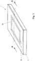
- Fig. 1 shows a mobile phone with a metallic housing according to the prior art.
- Fig. 2 is a cut through the in Fig. 1 illustrated mobile phone shown.
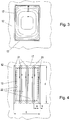
- Fig. 3 shows the formation of eddy currents in a fully metallic housing wall.
- Fig. 4 shows the formation of eddy currents in a preferred housing wall according to the invention.
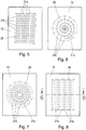
- Fig. 5 to 7 show preferred two-layer housing walls.
- Fig. 8 and 9 show a further two-layer embodiment of a housing wall in front view and in section.
- Fig. 10 shows a further advantageous embodiment of a housing wall, in which the slot field is used as a design element.
- Fig. 1 shows a mobile phone with a metallic housing according to the prior art.
- the mobile phone 1 has two housing parts 11, 12, namely a trough-like housing part 11 and a flat housing part 12, which assembled the electronics 14 (FIG. Fig. 2 ) of the mobile phone and shield.
- FIG. 1 an NFC antenna 13, which is connected to the electronics 14 of the mobile device and located inside the housing formed by the two housing parts 11, 12 of the mobile phone 1.
- an electromagnetic field is generated by the antenna 13.
- the dashed arrows 15 represent that electromagnetic field that arises without the metallic shielding of the housing wall 12.
- the dotted arrows 16 show the electromagnetic field produced by eddy currents 17, which are induced in the housing wall 12.
- 16 results in a resulting magnetic field 18, which is greatly attenuated compared to the original magnetic field 15.
- the range and strength of the magnetic field or data transmission, which is possible by means of NFC starting from the mobile phone 1, is therefore significantly reduced.
- Fig. 3 is the effect of current displacement in the housing wall 12 of the in Fig. 1 and 2 illustrated mobile phones 1 shown in more detail. It should be noted that, due to the effect of current displacement, the eddy currents that form are concentrated along the edge of the metal surface interspersed with the magnetic field.
- a sufficient suppression of eddy current induction can be achieved, however, if the flat structure of the metallic housing 11, 12, at least in the region of the inductive antenna 13 is designed so that eddy currents 17 can no longer or only to a very limited extent form therein.
- the easiest way is by the design of slots 21 in the metallic housing wall 11 in the region of the antenna 13, as in Fig. 4 shown, possible. These slots 21 can be arbitrarily thin, it only needs to come to a sufficient increase in the ohmic resistance in the transverse direction to the slots, as in Fig. 4 is shown schematically.
- the induced eddy currents 17 can not propagate unhindered ( 3 and 4 ). Of course, it comes in the individual webs 22 between the slots 21 for eddy current induction. Due to the comparatively small web width a, current paths through which flow is in the opposite direction are close to one another and compensate each other with regard to the mutual induction effect of the eddy currents. By selecting a small web width a, the mutual induction effect is further weakened. The housing wall 12 is all the more permeable to the magnetic field generated by the antenna 13, the smaller the land width a is selected.
- the portion of a metallic device housing covering the coil antenna 13 is provided with slots 21 as shown above, the magnetic field generated by the coil antenna 13 is no longer attenuated, so that wireless communication through inductive coupling through the metal housing 12 is possible through.
- the slot width b can be made very small without reducing the desired effect, it is also possible, for example by coating the Housing wall 12 with electrically non-electrically conductive materials to achieve a waterproof, or substantially airtight cover despite the slots 21. In this case, an electrically non-conductive material applied to the housing wall 12 bridges the slots 21, which each have only a very small slot width b.
- Fig. 5 to 7 show examples of housing walls 12 with arrangements of two over each other, but electrically isolated from each other arranged metal layers sufficiently suppress a mutual induction effect and thus allow inductive communication through the housing wall 12 therethrough.
- housing walls 12 are shown with two-layer slot fields, wherein in the first layer 23 (FIG. Fig. 9 ) the slits 21a shown in dashed lines and in the second layer 24 (FIG. Fig. 9 ) the dotted slots 21b are present.
- Fig. 8 shows such an embodiment, wherein Fig. 9 a cut CC in Fig. 8 shows.
- an insulating layer 25 is shown, which isolates the two layers 23, 24 to each other and prevents the ingress of liquids through the housing wall 12.
- Typical antennas 13 are designed for inductive data transmission in the frequency range between 10 kHz and 100 MHz, in particular 120-135 kHz, 13-14 MHz, 25-30 MHz.
- the mutual induction effect is locally influenced above all by the web widths a or slot spacings.
- web widths a with at most 3 mm make sense.
- the dimensions of the slot array 26, in particular the rectangular area of slot array length x slot array width, become larger than that Outside dimensions of the coil antenna 13 set.
- the slot array 26 projects beyond the coil antenna 13. Is the slot array 26 smaller than the outer dimensions the coil antenna 13 of the mobile phone, so at least one more communication with transponders is possible, the transponder antenna is smaller than the slot array 26.
- slot field 26 it is also possible to design the slot field 26 in such a way that it simultaneously fulfills advertising or brand identity or marketing purposes ( Fig. 10 ).
Landscapes
- Engineering & Computer Science (AREA)
- Signal Processing (AREA)
- Computer Networks & Wireless Communication (AREA)
- Physics & Mathematics (AREA)
- Microelectronics & Electronic Packaging (AREA)
- General Physics & Mathematics (AREA)
- Theoretical Computer Science (AREA)
- Computer Hardware Design (AREA)
- Acoustics & Sound (AREA)
- Near-Field Transmission Systems (AREA)
- Support Of Aerials (AREA)
Description
- Die Erfindung betrifft eine Gehäusewand für ein Datenkommunikationsgerät sowie ein Gehäuse für ein Datenkommunikationsgerät sowie ein mit einem Gehäuse ausgestattetes Datenkommunikationsgerät gemäß dem Oberbegriff des Patentanspruchs 1, 10 und 11.
- Grundsätzlich besteht bei Datenkommunikationsgeräten, wie z.B. Mobiltelefonen oder RFID-Lesegeräten, die eine drahtlose Datenübertragung basierend auf induktiver Kopplung zwischen dem Datenkommunikationsgerät und einem externen Gerät, wie z.B. einem NFC-Gerät oder einem Transponder, ermöglichen, das Problem, dass eine solche Datenübertragung mittels induktiver Kopplung nicht durch metallische bzw. elektrisch gut leitfähige Gehäuse, bzw. Objekte, bzw. Flächen hindurch funktioniert. Aus diesem Grund sind Datenkommunikationsgeräte wie beispielsweise Mobiltelefone mit metallischen Gehäusen in der Regel nicht geeignet, Datenübertragung mittels induktiver Kopplung mit einem externen Datenkommunikationsgerät durchzuführen. Grund dafür sind Gegeninduktionseffekte aufgrund von Wirbelströmen, die in den metallischen Objekten bzw. Flächen des Datenkommunikationsgerätes induziert werden. Das vom Sender erzeugte elektromagnetische Wechselfeld induziert im metallischen Gehäuse des Datenkommunikationsgeräts Wirbelströme, die ihrer Ursache entgegengerichtet sind und damit das resultierende für die Datenkommunikation notwendige Magnetfeld derart abschwächen, dass eine Datenkommunikation nicht möglich ist. Moderne Smartphones mit einer NFC-Schnittstelle haben daher im Bereich der NFC-Antenne, die sich normalerweise auf der Rückseite des Geräts befindet, ein nichtmetallisches Gehäuse bzw. eine nichtmetallische Abdeckung. Die Verwendung metallischer Gehäuse für Datenkommunikationsgeräte, insbesondere Mobiltelefone, hat jedoch gegenüber von nicht abschirmenden Kunststoffgehäusen vielerlei positive Aspekte und Vorteile, insbesondere im Hinblick auf Stabilität und Wärmeleitfähigkeit. Im Hinblick auf die auf induktiver Kopplung beruhende RFID- und NFC-Kommunikation, besteht dabei aber das Problem, dass die dafür verwendeten Magnetfelder nicht durchdringen können.
- Die
US 2009278757 A1 [AHN JUNG HO, et al.; 2009 ] zeigt ein mobiles Endgerät mit einem Metallgehäuse und einer im Inneren des Gehäuse liegenden Antennenstruktur. Die Antennenstruktur enthält eine Antenne zum Senden und zum Empfangen von hochfrequenten elektromagnetischen Wellen. Die Gehäusewand umfasst im Bereich der Antennenstruktur speziell zur Antenne ausgerichtete Schlitze , wobei die Schlitze, aufgrund ihrer speziellen Ausrichtung in Bezug auf die Antenne, bewirken, dass die von der Antenne ausgesendeten elektromagnetischen Wellen durch die Gehäusewand nach außen dringen können, und von außen elektromagnetische Wellen durch die Gehäusewand hindurch nach Innen zur Antenne dringen und damit von der Antenne empfangen werden können. Zur Realisierung dieser Eigenschaft, sind die Schlitze bezüglich Ihrer Geometrie auf die Sende- und Empfangsfrequenzen abgestimmt. - In ähnlicher Weise wird in
US 2012268343 A1 [YANAGI MASAHIRO, et al.; 2012 ] eine Antennenvorrichtung offenbart, die ein Gehäuse aus einem leitenden Material umfasst. In der Oberfläche des Gehäuses ist ein Schlitz- oder Schlitzfeld ausgebildet. Weites ist eine Antenne im Gehäuse angeordnet. Die Längsrichtung des Schlitzes ist in einem vorbestimmten Winkel in Bezug auf die Längsrichtung der Antenne ausgerichtet. - Aus der
US 2012276854 A1 [JOSHI HIMANSHU, et al.; 2012 ] ist eine implantierbare medizinische Vorrichtung bekannt die ein Gehäuse umfasst in der die Komponenten der Vorrichtung untergebracht sind. Im Gehäuse der Vorrichtung ist eine Schlitzantenne angeordnet, die mit einem externen Gerät durch die Aussparung hindurch zum Datenaustausch verbunden werden kann. - In der
EP 1027818 A1 [BOEHNKE GERD; 2000 ] wird eine Vorrichtung offenbart, die eine magnetische Abdeckung aufweist, die im wesentlichen undurchlässig für statische Magnetfelder ist. Die Abdeckung wird durch eine Anzahl von Öffnungen durchdrungen. Die Öffnungen begrenzen räumlich die durch dynamische Magnetfelder eines Wandlers hervorgerufenen Wirbelströme, welche sich dadurch nicht in voller Stärke ausbilden können. - Die Aufgabe der Erfindung ist es, eine Gehäusewand für ein Datenkommunikationsgerät insbesondere ein Mobiltelefon zu schaffen, die im Wesentlichen metallisch ist und die Stabilität und Wärmeleitfähigkeit von Metall aufweist, aber gleichzeitig für auf induktiver Kopplung basierende Datenübertragung durchlässig ist.
- Die Erfindung löst diese Aufgabe bei einer Gehäusewand der eingangs genannten Art mit den kennzeichnenden Merkmalen des Patentanspruchs 1.
- Erfindungsgemäß ist bei einer Gehäusewand für ein Datenkommunikationsgerät mit einem metallischen und elektrisch leitfähigen Grundkörper vorgesehen, dass in einem Bereich der Gehäusewand ein Schlitzfeld mit einer Anzahl von Schlitzen vorgesehen ist, sodass die Gehäusewand im Bereich des Schlitzfelds für Magnetfelder zur induktiven Signaleinkopplung zur drahtlosen Kommunikation durchlässig ist. Hierdurch wird eine einfache Möglichkeit geschaffen, eine Datenkommunikation zwischen einer im Bereich der Gehäusewand angeordneten Antenne und einem auf der gegenüberliegenden Seite angeordneten Datenkommunikationsgerät wie beispielsweise einem Transponder zu schaffen, wobei gleichzeitig die Vorteile eines metallischen Gehäuses wie beispielsweise die hohe Stabilität oder die geringe Störanfälligkeit weiter bestehen.
- Eine erhöhte mechanische Stabilität der erfindungsgemäßen Vorrichtung wird erreicht, wenn die Gehäusewand zumindest zweilagig aufgebaut ist und zumindest eine erste Lage und eine zweite Lage aufweist, die jeweils überlappende Schlitzbereiche mit Schlitzen aufweisen, wobei die Schlitze im Schlitzbereich gegeneinander versetzt angeordnet sind. Um gleichzeitig eine hohe mechanische Stabilität und eine geringe Unterdrückung des abgegebenen Magnetfelds zu erreichen, kann vorgesehen werden, dass zwischen der ersten Lage und der zweiten Lage eine Isolierschicht ausgebildet ist, die die beiden Lagen zueinander beabstandet und gegeneinander elektrisch isoliert.
- Um zusätzlich einen Wasser- oder Gaseintritt bzw. -durchtritt zu vermeiden, kann vorgesehen sein, dass die Gehäusewand im Bereich des Schlitzfeldes mit elektrisch nichtleitendem Material verschlossen ist, und insbesondere eine Isolierschicht aufweist, welche die Schlitze abdeckt und verschließt, wobei insbesondere das Schlitzfeld der Gehäusewand luft- oder wasserundurchlässig ist.
- Eine vorteilhafte Datenkommunikation durch die Gehäusewand hindurch wird erreicht, wenn an einer ihrer Seiten im Bereich des Schlitzfelds eine Spulenantenne angeordnet ist
- Um eine Abschirmung des von einer Antenne abgegebenen Magnetfelds weiter zu verhindern, kann vorgesehen sein, dass das Schlitzfeld die Spulenantenne überragt.
- Eine vorteilhafte Unterdrückung der Gegeninduktion wird erreicht, wenn die zwischen den Schlitzen ausgebildeten Stege eine Breite von höchstens 3 mm aufweisen.
- Die Mechanische Stabilität kann weiter verbessert werden, indem die Schlitze der ersten Lage und die Schlitze der zweiten Lage zueinander Winkel von mehr als 45°, insbesondere von mehr als 85°, einschließen.
- Die Erfindung betrifft ferner ein Gehäuse für ein Datenkommunikationsgerät umfassend eine Gehäusewand nach einem der vorangehenden Ansprüche sowie eine im Inneren des Gehäuses, im Bereich des Schlitzfelds angeordnete Spulenantenne.
- Weiters betrifft die Erfindung ein Datenkommunikationsgerät, insbesondere Mobiltelefon, mit einem Gehäuse nach Anspruch 10.
- Mehrere Ausführungsbeispiele der Erfindung sind anhand der folgenden Zeichnungsfiguren dargestellt.
-
Fig. 1 zeigt ein Mobiltelefon mit einem metallischen Gehäuse gemäß dem Stand der Technik. InFig. 2 ist ein Schnitt durch das inFig. 1 dargestellte Mobiltelefon dargestellt.Fig. 3 zeigt die Ausbildung von Wirbelströmen in einer vollmetallischen Gehäusewand.Fig. 4 zeigt die Ausbildung von Wirbelströmen in einer bevorzugten erfindungsgemäßen Gehäusewand.Fig. 5 bis 7 zeigen bevorzugte zweilagige Gehäusewände.Fig. 8 und9 zeigen eine weitere zweilagige Ausführungsform einer Gehäusewand in Vorderansicht sowie im Schnitt.Fig. 10 zeigt eine weitere vorteilhafte Ausbildung einer Gehäusewand, bei der das Schlitzfeld als Designelement verwendet wird. -
Fig. 1 zeigt ein Mobiltelefon mit einem metallischen Gehäuse gemäß dem Stand der Technik. Im vorliegenden Beispiel weist das Mobiltelefon 1 zwei Gehäuseteile 11, 12, nämlich einen wannenartigen Gehäuseteil 11 und einen flachen Gehäuseteil 12 auf, die zusammengesetzt die Elektronik 14 (Fig. 2 ) des Mobiltelefons umschließen und abschirmen. - Weiters zeigt
Fig. 1 eine NFC-Antenne 13, die mit der Elektronik 14 des Mobilfunkgeräts verbunden ist und im Inneren des durch die beiden Gehäuseteile 11, 12 gebildeten Gehäuses des Mobiltelefons 1 liegt. - Wie in
Fig. 2 dargestellt, wird durch die Antenne 13 ein elektromagnetisches Feld erzeugt. Die strichlierten Pfeile 15 stellen dasjenige elektromagnetische Feld dar, das ohne die metallische Abschirmung der Gehäusewand 12 entsteht. Die punktierten Pfeile 16 zeigen das elektromagnetische Feld, das durch Wirbelströme 17 entsteht, die in der Gehäusewand 12 induziert werden. Als Resultat der Überlagerung der beiden Magnetfelder 15, 16 ergibt sich ein resultierendes Magnetfeld 18, das gegenüber dem ursprünglichen Magnetfeld 15 stark abgeschwächt ist. Die Reichweite und Stärke des Magnetfelds bzw. der Datenübertragung, die mittels NFC ausgehend von dem Mobiltelefon 1 möglich ist, ist daher deutlich reduziert. - Um das Ziel eines für eine induktive Kommunikation ausreichenden resultierenden Magnetfeldes außerhalb des Mobiltelefongehäuses zu erreichen, kann die Ausbildung der Wirbelstrominduktion unterdrückt werden. Eine Verminderung der elektrischen Leitfähigkeit des Materials der Gerätegehäuse-Rückwand ist mit gegenwärtig technisch verfügbaren Materialien nicht möglich ohne gleichzeitig auch viele (thermische) Vorteile einer metallischen Gerätegehäuse-Rückwand zu verlieren.
- In
Fig. 3 ist der Effekt der Stromverdrängung in der Gehäusewand 12 des inFig. 1 und2 dargestellten Mobiltelefons 1 näher dargestellt. Zu beachten ist, dass die sich ausbildenden Wirbelströme zufolge des Effekts der Stromverdrängung, sich entlang des Randes der vom Magnetfeld durchsetzten Metallfläche konzentrieren. - Eine ausreichende Unterdrückung der Wirbelstrominduktion kann jedoch erreicht werden, wenn die flächige Struktur des metallischen Gehäuses 11, 12, zumindest im Bereich der induktiven Antenne 13 so gestaltet wird, dass sich Wirbelströme 17 nicht mehr oder nur mehr in sehr eingeschränktem Ausmaß darin ausbilden können. Am einfachsten ist dies durch die Ausgestaltung von Schlitzen 21 in der metallischen Gehäusewand 11 im Bereich der Antenne 13, wie in
Fig. 4 dargestellt, möglich. Diese Schlitze 21 können beliebig dünn sein, es braucht nur zu einer ausreichenden Erhöhung des ohmschen Widerstandes in Querrichtung zu den Schlitzen kommen, wie dies inFig. 4 schematisch dargestellt ist. - Aufgrund der Schlitze im Metall können sich die induzierten Wirbelströme 17 nicht ungehindert ausbreiten (
Fig. 3 und 4 ). Natürlich kommt es in den einzelnen Stegen 22 zwischen den Schlitzen 21 zur Wirbelstrominduktion. Aufgrund der vergleichsweise geringen Stegbreite a liegen gegensinnig durchflossene Strompfade nah beieinander und kompensieren einander hinsichtlich der Gegeninduktionswirkung der Wirbelströme. Durch Auswahl einer geringen Stegbreite a wird die Gegeninduktionswirkung weiter abgeschwächt. Die Gehäusewand 12 wird umso durchlässiger für das von der Antenne 13 erzeugte Magnetfeld, je kleiner die Stegbreite a gewählt wird. - Wird jener Bereich eines metallischen Gerätegehäuses der die Spulenantenne 13 abdeckt, wie oben gezeigt mit Schlitzen 21 versehen, wird auch das von der Spulenantenne 13 erzeugte Magnetfeld nicht mehr, bzw. nur mehr geringfügig abgeschwächt, so dass eine drahtlose Kommunikation durch induktive Kopplung durch das Metallgehäuse 12 hindurch möglich ist.
- Da die Schlitzbreite b sehr klein ausgeführt sein kann ohne den gewünschten Effekt zu mindern, besteht auch die Möglichkeit, beispielsweise durch Beschichtung der Gehäusewand 12 mit elektrisch nicht-elektrisch leitfähigen Materialien, eine wasserdichte, bzw. weitgehend luftdichte Abdeckung trotz der Schlitze 21 zu erzielen. Hierbei überbrückt ein auf die Gehäusewand 12 aufgebrachtes elektrisch nicht-leitfähiges Material die Schlitze 21, die jeweils nur eine sehr geringe Schlitzbreite b aufweisen.
-
Fig. 5 bis 7 zeigen Beispiele von Gehäusewänden 12 mit Anordnungen zweier übereinander, jedoch elektrisch voneinander isoliert angeordneter Metallschichten, die eine Gegeninduktionswirkung ausreichend unterdrücken und damit eine induktive Kommunikation durch die Gehäusewand 12 hindurch ermöglichen. - In den
Fig. 5 bis 7 sind mehrere Ausführungsformen von Gehäusewänden 12 mit zweilagigen Schlitzfeldern dargestellt, wobei in der ersten Lage 23 (Fig. 9 ) die strichliert dargestellten Schlitze 21a und in der zweiten Lage 24 (Fig. 9 ) die punktiert dargestellten Schlitze 21b vorhanden sind. - Die durch Schlitze 21 verursachte Antennenwirkung kann insbesondere im UHF und Mikrowellenbereich auch mit zwei Lagen 23, 24 geschlitzter, gegeneinander elektrisch isolierter Metallschichten in einer Anordnung gemäß
Fig. 8 und9 unterdrückt werden.Fig. 8 zeigt eine solche Ausführungsform, wobeiFig. 9 einen Schnitt C-C inFig. 8 zeigt. Hier ist eine Isolierschicht 25 dargestellt, die die beiden Lagen 23, 24 zueinander isoliert und das Eindringen von Flüssigkeiten durch die Gehäusewand 12 verhindert. - Typische Antennen 13 sind für induktive Datenübertragung im Frequenzbereich zwischen 10 kHz und 100 MHz, insbesondere 120-135 kHz, 13-14 MHz, 25-30 MHz ausgebildet.
- Die Gegeninduktionswirkung wird lokal vor allem durch die Stegbreiten a bzw. Schlitzabstände beeinflusst. Je kleiner die Stegbreiten a, desto besser wird die Gegeninduktionswirkung unterdrückt. In der Praxis erscheinen Stegbreiten a mit höchstens 3 mm sinnvoll.
- Für uneingeschränkten Betrieb der induktiven Datenkommunikation, wobei Kommunikation mit allen Transpondergrößen möglich ist, so wie es auch im Fall eines nicht-metallischen Gehäuses der Fall wäre, werden die Abmessungen des Schlitzfeldes 26, insbesondere die rechteckige Fläche der Größe Schlitzfeldlänge x Schlitzfeldbreite, größer als die Außenabmessungen der Spulenantenne 13 festgelegt. Das Schlitzfeld 26 überragt die Spulenantenne 13. Ist das Schlitzfeld 26 kleiner als die Außenabmessungen der Spulenantenne 13 des Mobiltelefons, so ist zumindest noch eine Kommunikation mit Transpondern möglich, deren Transponderantenne kleiner als das Schlitzfeld 26 ist.
- Es ist natürlich auch möglich, das Schlitzfeld 26 so zu gestalten, dass es gleichzeitig auch Werbe- bzw. Markenidentitäts- bzw. Marketingzwecke erfüllt (
Fig. 10 ).
Claims (11)
- Gehäusewand (12) für ein Datenkommunikationsgerät (1) mit einem metallischen und elektrisch leitfähigen Grundkörper,
wobei in einem Bereich der Gehäusewand (12) ein Schlitzfeld (26) mit einer Anzahl von Schlitzen (21) vorgesehen ist, sodass die Gehäusewand (12) im Bereich des Schlitzfelds (26) für Magnetfelder zur induktiven Signaleinkopplung zur drahtlosen Kommunikation durchlässig ist,
wobei die Gehäusewand zumindest zweilagig aufgebaut ist und zumindest eine erste Lage (23) und eine zweite Lage (24) aufweist bei denen jeweils innerhalb eines gemeinsamen Schlitzbereichs (26) Schlitze (21a, 21b) vorhanden sind
dadurch gekennzeichnet,- dass im Schlitzbereich (26) die Schlitze (21a) der ersten Lage (23) zu den Schlitzen (21b) der zweiten Lage (24) versetzt angeordnet sind, und- dass zwischen der ersten Lage (23) und der zweiten Lage (24) eine Isolierschicht (25) ausgebildet ist, die die beiden Lagen (23, 24) zueinander beabstandet und gegeneinander elektrisch isoliert. - Gehäusewand (12) nach Anspruch 1, dadurch gekennzeichnet, dass die Gehäusewand (12) im Bereich des Schlitzfeldes (26) mit elektrisch nichtleitendem Material verschlossen ist.
- Gehäusewand (12) nach Anspruch 1 oder 2, dadurch gekennzeichnet, dass die Gehäusewand (12) eine Isolierschicht (25) aufweist, welche die Schlitze (21) abdeckt und verschließt.
- Gehäusewand (12) Anspruch 3, dadurch gekennzeichnet, dass das Schlitzfeld (26) der Gehäusewand (12) luft- oder wasserundurchlässig ist.
- Gehäusewand (12) nach einem der vorangehenden Ansprüche, dadurch gekennzeichnet, dass an einer ihrer Seiten im Bereich des Schlitzfelds (26) eine Spulenantenne (13) angeordnet ist.
- Gehäusewand (12) nach einem der vorangehenden Ansprüche, dadurch gekennzeichnet, dass das Schlitzfeld (26) die Spulenantenne (13) überragt.
- Gehäusewand (12) nach einem der vorangehenden Ansprüche, dadurch gekennzeichnet, dass die zwischen den Schlitzen (21) ausgebildeten Stege (22) eine Breite von höchstens 3 mm aufweisen.
- Gehäusewand (12) nach einem der vorangehenden Ansprüche, dadurch gekennzeichnet, dass die Schlitze (21a) der ersten Lage (23) und die Schlitze (21b) der zweiten Lage (21b) zueinander Winkel von mehr als 45° einschließen.
- Gehäusewand (12) nach einem der vorangehenden Ansprüche, dadurch gekennzeichnet, dass die Schlitze (21a) der ersten Lage (23) und die Schlitze (21b) der zweiten Lage (21b) zueinander Winkel von mehr als 85° einschließen.
- Gehäuse (11, 12) für ein Datenkommunikationsgerät (1) umfassend eine Gehäusewand (12) nach einem der vorangehenden Ansprüche sowie eine im Inneren des Gehäuses (11, 12) angeordnete, im Bereich des Schlitzfelds (26) angeordnete Spulenantenne (13).
- Datenkommunikationsgerät, insbesondere Mobiltelefon (1), mit einem Gehäuse (11, 12) nach Anspruch 10.
Applications Claiming Priority (2)
| Application Number | Priority Date | Filing Date | Title |
|---|---|---|---|
| ATA50467/2013A AT514622B1 (de) | 2013-07-24 | 2013-07-24 | Gehäusewand |
| PCT/AT2014/050154 WO2015010147A1 (de) | 2013-07-24 | 2014-07-04 | Gehäusewand |
Publications (2)
| Publication Number | Publication Date |
|---|---|
| EP2941861A1 EP2941861A1 (de) | 2015-11-11 |
| EP2941861B1 true EP2941861B1 (de) | 2018-02-28 |
Family
ID=51265440
Family Applications (1)
| Application Number | Title | Priority Date | Filing Date |
|---|---|---|---|
| EP14747291.4A Not-in-force EP2941861B1 (de) | 2013-07-24 | 2014-07-04 | Gehäusewand |
Country Status (4)
| Country | Link |
|---|---|
| US (1) | US9756155B2 (de) |
| EP (1) | EP2941861B1 (de) |
| AT (1) | AT514622B1 (de) |
| WO (1) | WO2015010147A1 (de) |
Families Citing this family (7)
| Publication number | Priority date | Publication date | Assignee | Title |
|---|---|---|---|---|
| US9083073B2 (en) | 2012-06-28 | 2015-07-14 | Intel Corporation | Thin chassis near field communication (NFC) antenna integration |
| WO2014167812A1 (ja) * | 2013-04-12 | 2014-10-16 | パナソニック株式会社 | アンテナ、アンテナ装置および通信装置 |
| DE102015221281A1 (de) * | 2015-10-30 | 2017-05-04 | Osram Gmbh | Drahtlos programmierbares elektronisches Betriebsgerät |
| KR101887891B1 (ko) * | 2016-02-17 | 2018-08-13 | 주식회사 아모센스 | 휴대단말기용 백커버 및 이를 포함하는 백커버 일체형 안테나모듈 |
| WO2018028486A1 (en) * | 2016-08-08 | 2018-02-15 | Guangdong Oppo Mobile Telecommunications Corp., Ltd. | Housing, method for manufacturing housing, and mobile terminal having housing |
| AT519728A1 (de) * | 2017-03-09 | 2018-09-15 | Seibersdorf Labor Gmbh | Deaktivierbares Abschirmelement |
| IT202000017464A1 (it) * | 2020-07-17 | 2022-01-17 | Vimar Spa | Dispositivo di intercomunicazione comprendente un dispositivo di ausilio per audiolesi |
Family Cites Families (10)
| Publication number | Priority date | Publication date | Assignee | Title |
|---|---|---|---|---|
| DE19747562C2 (de) * | 1997-10-28 | 2000-09-28 | Siemens Ag | Verfahren und Anordnung zum Steuern der Ausbreitung von Magnetfeldern durch elektrodynamische/-magnetische Wandler, insbesondere in Telekommunikationsgeräten |
| FR2803482B1 (fr) * | 2000-01-05 | 2002-02-15 | Diffusion Vente Internationale | Lecteur pour cle electronique |
| JP2003035786A (ja) * | 2001-07-25 | 2003-02-07 | Mitsubishi Materials Corp | タグ内蔵腕時計 |
| ATE365982T1 (de) * | 2002-11-13 | 2007-07-15 | Mitsubishi Materials Corp | Armbanduhr mit einem rfid-etikett |
| KR101501921B1 (ko) * | 2008-05-06 | 2015-03-13 | 삼성전자주식회사 | 금속 케이스를 갖는 휴대 단말기 및 그의 안테나 구조 |
| JP2012231266A (ja) * | 2011-04-25 | 2012-11-22 | Fujitsu Component Ltd | アンテナ装置 |
| US9259582B2 (en) * | 2011-04-29 | 2016-02-16 | Cyberonics, Inc. | Slot antenna for an implantable device |
| EP2562868A1 (de) * | 2011-08-22 | 2013-02-27 | Laird Technologies AB | Mehrschleifige Rahmenantennenanordnung und tragbare Funkkommunikationsvorrichtung mit solch einer Anordnung |
| EP2587638A1 (de) * | 2011-10-26 | 2013-05-01 | Siemens Aktiengesellschaft | Außenglimmschutz für eine elektrische Maschine |
| CN202748817U (zh) * | 2011-11-30 | 2013-02-20 | 北京物资学院 | 一种螺旋式定向接收的无线射频标签 |
-
2013
- 2013-07-24 AT ATA50467/2013A patent/AT514622B1/de not_active IP Right Cessation
-
2014
- 2014-07-04 US US14/907,194 patent/US9756155B2/en not_active Expired - Fee Related
- 2014-07-04 WO PCT/AT2014/050154 patent/WO2015010147A1/de not_active Ceased
- 2014-07-04 EP EP14747291.4A patent/EP2941861B1/de not_active Not-in-force
Also Published As
| Publication number | Publication date |
|---|---|
| WO2015010147A1 (de) | 2015-01-29 |
| AT514622B1 (de) | 2015-08-15 |
| AT514622A1 (de) | 2015-02-15 |
| US20160165018A1 (en) | 2016-06-09 |
| EP2941861A1 (de) | 2015-11-11 |
| US9756155B2 (en) | 2017-09-05 |
Similar Documents
| Publication | Publication Date | Title |
|---|---|---|
| AT514622B1 (de) | Gehäusewand | |
| DE102013209763B4 (de) | Berührungsbedienfeld-Aufbau, Berührungs- und Anzeigebedienfeld-Aufbau und Antennenstruktur aufweisender integrierter Berührungsanzeigebedienfeld-Aufbau und Verfahren zur Bildung eines Antennenstruktur aufweisenden Berührungsbedienfeldes | |
| EP0594809B1 (de) | Funkantennenanordnung in der nähe von fahrzeug-fensterscheiben | |
| DE69220344T2 (de) | Tragbare Funk- und Funktelefongeräte mit Schlitzen darin | |
| DE102010028992B4 (de) | Antennenvorrichtung, Transponderlesegerät, Induktionsherd | |
| DE112017008372B4 (de) | Antennenvorrichtung | |
| DE10353686A1 (de) | Symmetrische Antenne in Schichtbauweise | |
| DE112018007422T5 (de) | Wellenleiter-schlitzgruppenantenne | |
| DE112013002000T5 (de) | Antennenvorrichtung | |
| DE202017104142U1 (de) | Miniatur-Breitbandantenne mit parasitärem Element | |
| DE112004002040T5 (de) | Antennenelement sowie das Antennenelement verwendende Schleifenantenne und Kommunikations-Steuervorrichtung für ein drahtloses Kommunikationsmedium | |
| DE112014006598T5 (de) | Antennenvorrichtung und Herstellungsverfahren für die Antennenvorrichtung | |
| DE102021206859A1 (de) | Radarvorrichtung | |
| EP2529338B1 (de) | Tragbarer datenträger mit funkbasierter datenkommunikationseinrichtung | |
| DE102013201222A1 (de) | Antennenvorrichtung | |
| EP2367233A1 (de) | Planares Antennensystem | |
| EP3036793B1 (de) | Vorrichtung und verfahren zur kombinierten signalübertragung oder zur kombinierten signal- und energieübertragung | |
| DE112016000113T5 (de) | NFC-Antenne des Oberflächenmontagetyps und Antennensystem | |
| WO2007131879A1 (de) | Testvorrichtung mit hf-/uhf-dualbandantenne zum testen von rfid-transpondern in einem fertigungsgerät | |
| EP2618425B1 (de) | Antennenabdeckung | |
| DE102010033996A1 (de) | Tragbarer Datenträger mit über Spulenkopplung arbeitender Datenkommunikationseinrichtung | |
| EP2738715B1 (de) | Tube Tag | |
| DE102011090139A1 (de) | Sendeanordnung für eine Funkstation und Funkstation | |
| DE112021002461T5 (de) | Antennenvorrichtung, und drahtlose kommunikationsvorrichtung | |
| EP2907945B1 (de) | Kommunikationseinrichtungen |
Legal Events
| Date | Code | Title | Description |
|---|---|---|---|
| PUAI | Public reference made under article 153(3) epc to a published international application that has entered the european phase |
Free format text: ORIGINAL CODE: 0009012 |
|
| 17P | Request for examination filed |
Effective date: 20150805 |
|
| AK | Designated contracting states |
Kind code of ref document: A1 Designated state(s): AL AT BE BG CH CY CZ DE DK EE ES FI FR GB GR HR HU IE IS IT LI LT LU LV MC MK MT NL NO PL PT RO RS SE SI SK SM TR |
|
| AX | Request for extension of the european patent |
Extension state: BA ME |
|
| 17Q | First examination report despatched |
Effective date: 20160204 |
|
| DAX | Request for extension of the european patent (deleted) | ||
| GRAP | Despatch of communication of intention to grant a patent |
Free format text: ORIGINAL CODE: EPIDOSNIGR1 |
|
| STAA | Information on the status of an ep patent application or granted ep patent |
Free format text: STATUS: GRANT OF PATENT IS INTENDED |
|
| INTG | Intention to grant announced |
Effective date: 20170601 |
|
| GRAJ | Information related to disapproval of communication of intention to grant by the applicant or resumption of examination proceedings by the epo deleted |
Free format text: ORIGINAL CODE: EPIDOSDIGR1 |
|
| STAA | Information on the status of an ep patent application or granted ep patent |
Free format text: STATUS: EXAMINATION IS IN PROGRESS |
|
| INTC | Intention to grant announced (deleted) | ||
| GRAP | Despatch of communication of intention to grant a patent |
Free format text: ORIGINAL CODE: EPIDOSNIGR1 |
|
| STAA | Information on the status of an ep patent application or granted ep patent |
Free format text: STATUS: GRANT OF PATENT IS INTENDED |
|
| INTG | Intention to grant announced |
Effective date: 20170918 |
|
| GRAS | Grant fee paid |
Free format text: ORIGINAL CODE: EPIDOSNIGR3 |
|
| GRAA | (expected) grant |
Free format text: ORIGINAL CODE: 0009210 |
|
| STAA | Information on the status of an ep patent application or granted ep patent |
Free format text: STATUS: THE PATENT HAS BEEN GRANTED |
|
| AK | Designated contracting states |
Kind code of ref document: B1 Designated state(s): AL AT BE BG CH CY CZ DE DK EE ES FI FR GB GR HR HU IE IS IT LI LT LU LV MC MK MT NL NO PL PT RO RS SE SI SK SM TR |
|
| REG | Reference to a national code |
Ref country code: GB Ref legal event code: FG4D Free format text: NOT ENGLISH Ref country code: CH Ref legal event code: EP |
|
| REG | Reference to a national code |
Ref country code: AT Ref legal event code: REF Ref document number: 975340 Country of ref document: AT Kind code of ref document: T Effective date: 20180315 |
|
| REG | Reference to a national code |
Ref country code: IE Ref legal event code: FG4D Free format text: LANGUAGE OF EP DOCUMENT: GERMAN |
|
| REG | Reference to a national code |
Ref country code: DE Ref legal event code: R096 Ref document number: 502014007452 Country of ref document: DE |
|
| REG | Reference to a national code |
Ref country code: NL Ref legal event code: MP Effective date: 20180228 |
|
| REG | Reference to a national code |
Ref country code: LT Ref legal event code: MG4D |
|
| REG | Reference to a national code |
Ref country code: FR Ref legal event code: PLFP Year of fee payment: 5 |
|
| PG25 | Lapsed in a contracting state [announced via postgrant information from national office to epo] |
Ref country code: ES Free format text: LAPSE BECAUSE OF FAILURE TO SUBMIT A TRANSLATION OF THE DESCRIPTION OR TO PAY THE FEE WITHIN THE PRESCRIBED TIME-LIMIT Effective date: 20180228 Ref country code: HR Free format text: LAPSE BECAUSE OF FAILURE TO SUBMIT A TRANSLATION OF THE DESCRIPTION OR TO PAY THE FEE WITHIN THE PRESCRIBED TIME-LIMIT Effective date: 20180228 Ref country code: NO Free format text: LAPSE BECAUSE OF FAILURE TO SUBMIT A TRANSLATION OF THE DESCRIPTION OR TO PAY THE FEE WITHIN THE PRESCRIBED TIME-LIMIT Effective date: 20180528 Ref country code: FI Free format text: LAPSE BECAUSE OF FAILURE TO SUBMIT A TRANSLATION OF THE DESCRIPTION OR TO PAY THE FEE WITHIN THE PRESCRIBED TIME-LIMIT Effective date: 20180228 Ref country code: CY Free format text: LAPSE BECAUSE OF FAILURE TO SUBMIT A TRANSLATION OF THE DESCRIPTION OR TO PAY THE FEE WITHIN THE PRESCRIBED TIME-LIMIT Effective date: 20180228 Ref country code: LT Free format text: LAPSE BECAUSE OF FAILURE TO SUBMIT A TRANSLATION OF THE DESCRIPTION OR TO PAY THE FEE WITHIN THE PRESCRIBED TIME-LIMIT Effective date: 20180228 Ref country code: NL Free format text: LAPSE BECAUSE OF FAILURE TO SUBMIT A TRANSLATION OF THE DESCRIPTION OR TO PAY THE FEE WITHIN THE PRESCRIBED TIME-LIMIT Effective date: 20180228 |
|
| PG25 | Lapsed in a contracting state [announced via postgrant information from national office to epo] |
Ref country code: RS Free format text: LAPSE BECAUSE OF FAILURE TO SUBMIT A TRANSLATION OF THE DESCRIPTION OR TO PAY THE FEE WITHIN THE PRESCRIBED TIME-LIMIT Effective date: 20180228 Ref country code: LV Free format text: LAPSE BECAUSE OF FAILURE TO SUBMIT A TRANSLATION OF THE DESCRIPTION OR TO PAY THE FEE WITHIN THE PRESCRIBED TIME-LIMIT Effective date: 20180228 Ref country code: SE Free format text: LAPSE BECAUSE OF FAILURE TO SUBMIT A TRANSLATION OF THE DESCRIPTION OR TO PAY THE FEE WITHIN THE PRESCRIBED TIME-LIMIT Effective date: 20180228 Ref country code: GR Free format text: LAPSE BECAUSE OF FAILURE TO SUBMIT A TRANSLATION OF THE DESCRIPTION OR TO PAY THE FEE WITHIN THE PRESCRIBED TIME-LIMIT Effective date: 20180529 Ref country code: BG Free format text: LAPSE BECAUSE OF FAILURE TO SUBMIT A TRANSLATION OF THE DESCRIPTION OR TO PAY THE FEE WITHIN THE PRESCRIBED TIME-LIMIT Effective date: 20180528 |
|
| PG25 | Lapsed in a contracting state [announced via postgrant information from national office to epo] |
Ref country code: MT Free format text: LAPSE BECAUSE OF FAILURE TO SUBMIT A TRANSLATION OF THE DESCRIPTION OR TO PAY THE FEE WITHIN THE PRESCRIBED TIME-LIMIT Effective date: 20180228 |
|
| PG25 | Lapsed in a contracting state [announced via postgrant information from national office to epo] |
Ref country code: AL Free format text: LAPSE BECAUSE OF FAILURE TO SUBMIT A TRANSLATION OF THE DESCRIPTION OR TO PAY THE FEE WITHIN THE PRESCRIBED TIME-LIMIT Effective date: 20180228 Ref country code: RO Free format text: LAPSE BECAUSE OF FAILURE TO SUBMIT A TRANSLATION OF THE DESCRIPTION OR TO PAY THE FEE WITHIN THE PRESCRIBED TIME-LIMIT Effective date: 20180228 Ref country code: IT Free format text: LAPSE BECAUSE OF FAILURE TO SUBMIT A TRANSLATION OF THE DESCRIPTION OR TO PAY THE FEE WITHIN THE PRESCRIBED TIME-LIMIT Effective date: 20180228 Ref country code: EE Free format text: LAPSE BECAUSE OF FAILURE TO SUBMIT A TRANSLATION OF THE DESCRIPTION OR TO PAY THE FEE WITHIN THE PRESCRIBED TIME-LIMIT Effective date: 20180228 Ref country code: PL Free format text: LAPSE BECAUSE OF FAILURE TO SUBMIT A TRANSLATION OF THE DESCRIPTION OR TO PAY THE FEE WITHIN THE PRESCRIBED TIME-LIMIT Effective date: 20180228 |
|
| REG | Reference to a national code |
Ref country code: DE Ref legal event code: R097 Ref document number: 502014007452 Country of ref document: DE |
|
| PG25 | Lapsed in a contracting state [announced via postgrant information from national office to epo] |
Ref country code: SK Free format text: LAPSE BECAUSE OF FAILURE TO SUBMIT A TRANSLATION OF THE DESCRIPTION OR TO PAY THE FEE WITHIN THE PRESCRIBED TIME-LIMIT Effective date: 20180228 Ref country code: CZ Free format text: LAPSE BECAUSE OF FAILURE TO SUBMIT A TRANSLATION OF THE DESCRIPTION OR TO PAY THE FEE WITHIN THE PRESCRIBED TIME-LIMIT Effective date: 20180228 Ref country code: DK Free format text: LAPSE BECAUSE OF FAILURE TO SUBMIT A TRANSLATION OF THE DESCRIPTION OR TO PAY THE FEE WITHIN THE PRESCRIBED TIME-LIMIT Effective date: 20180228 Ref country code: SM Free format text: LAPSE BECAUSE OF FAILURE TO SUBMIT A TRANSLATION OF THE DESCRIPTION OR TO PAY THE FEE WITHIN THE PRESCRIBED TIME-LIMIT Effective date: 20180228 |
|
| PLBE | No opposition filed within time limit |
Free format text: ORIGINAL CODE: 0009261 |
|
| STAA | Information on the status of an ep patent application or granted ep patent |
Free format text: STATUS: NO OPPOSITION FILED WITHIN TIME LIMIT |
|
| 26N | No opposition filed |
Effective date: 20181129 |
|
| PG25 | Lapsed in a contracting state [announced via postgrant information from national office to epo] |
Ref country code: SI Free format text: LAPSE BECAUSE OF FAILURE TO SUBMIT A TRANSLATION OF THE DESCRIPTION OR TO PAY THE FEE WITHIN THE PRESCRIBED TIME-LIMIT Effective date: 20180228 |
|
| REG | Reference to a national code |
Ref country code: CH Ref legal event code: PL |
|
| PG25 | Lapsed in a contracting state [announced via postgrant information from national office to epo] |
Ref country code: MC Free format text: LAPSE BECAUSE OF FAILURE TO SUBMIT A TRANSLATION OF THE DESCRIPTION OR TO PAY THE FEE WITHIN THE PRESCRIBED TIME-LIMIT Effective date: 20180228 Ref country code: LU Free format text: LAPSE BECAUSE OF NON-PAYMENT OF DUE FEES Effective date: 20180704 |
|
| REG | Reference to a national code |
Ref country code: BE Ref legal event code: MM Effective date: 20180731 |
|
| REG | Reference to a national code |
Ref country code: IE Ref legal event code: MM4A |
|
| PG25 | Lapsed in a contracting state [announced via postgrant information from national office to epo] |
Ref country code: CH Free format text: LAPSE BECAUSE OF NON-PAYMENT OF DUE FEES Effective date: 20180731 Ref country code: LI Free format text: LAPSE BECAUSE OF NON-PAYMENT OF DUE FEES Effective date: 20180731 Ref country code: IE Free format text: LAPSE BECAUSE OF NON-PAYMENT OF DUE FEES Effective date: 20180704 |
|
| PG25 | Lapsed in a contracting state [announced via postgrant information from national office to epo] |
Ref country code: BE Free format text: LAPSE BECAUSE OF NON-PAYMENT OF DUE FEES Effective date: 20180731 |
|
| PGFP | Annual fee paid to national office [announced via postgrant information from national office to epo] |
Ref country code: FR Payment date: 20190719 Year of fee payment: 6 Ref country code: DE Payment date: 20190719 Year of fee payment: 6 |
|
| PGFP | Annual fee paid to national office [announced via postgrant information from national office to epo] |
Ref country code: GB Payment date: 20190719 Year of fee payment: 6 |
|
| PG25 | Lapsed in a contracting state [announced via postgrant information from national office to epo] |
Ref country code: TR Free format text: LAPSE BECAUSE OF FAILURE TO SUBMIT A TRANSLATION OF THE DESCRIPTION OR TO PAY THE FEE WITHIN THE PRESCRIBED TIME-LIMIT Effective date: 20180228 |
|
| PG25 | Lapsed in a contracting state [announced via postgrant information from national office to epo] |
Ref country code: PT Free format text: LAPSE BECAUSE OF FAILURE TO SUBMIT A TRANSLATION OF THE DESCRIPTION OR TO PAY THE FEE WITHIN THE PRESCRIBED TIME-LIMIT Effective date: 20180228 |
|
| PG25 | Lapsed in a contracting state [announced via postgrant information from national office to epo] |
Ref country code: HU Free format text: LAPSE BECAUSE OF FAILURE TO SUBMIT A TRANSLATION OF THE DESCRIPTION OR TO PAY THE FEE WITHIN THE PRESCRIBED TIME-LIMIT; INVALID AB INITIO Effective date: 20140704 Ref country code: MK Free format text: LAPSE BECAUSE OF NON-PAYMENT OF DUE FEES Effective date: 20180228 |
|
| PG25 | Lapsed in a contracting state [announced via postgrant information from national office to epo] |
Ref country code: IS Free format text: LAPSE BECAUSE OF FAILURE TO SUBMIT A TRANSLATION OF THE DESCRIPTION OR TO PAY THE FEE WITHIN THE PRESCRIBED TIME-LIMIT Effective date: 20180628 |
|
| REG | Reference to a national code |
Ref country code: AT Ref legal event code: MM01 Ref document number: 975340 Country of ref document: AT Kind code of ref document: T Effective date: 20190704 |
|
| PG25 | Lapsed in a contracting state [announced via postgrant information from national office to epo] |
Ref country code: AT Free format text: LAPSE BECAUSE OF NON-PAYMENT OF DUE FEES Effective date: 20190704 |
|
| REG | Reference to a national code |
Ref country code: DE Ref legal event code: R119 Ref document number: 502014007452 Country of ref document: DE |
|
| GBPC | Gb: european patent ceased through non-payment of renewal fee |
Effective date: 20200704 |
|
| PG25 | Lapsed in a contracting state [announced via postgrant information from national office to epo] |
Ref country code: FR Free format text: LAPSE BECAUSE OF NON-PAYMENT OF DUE FEES Effective date: 20200731 Ref country code: GB Free format text: LAPSE BECAUSE OF NON-PAYMENT OF DUE FEES Effective date: 20200704 |
|
| PG25 | Lapsed in a contracting state [announced via postgrant information from national office to epo] |
Ref country code: DE Free format text: LAPSE BECAUSE OF NON-PAYMENT OF DUE FEES Effective date: 20210202 |