EP2941094A1 - An apparatus and method for stabilizing an average current of an LED lamp - Google Patents
An apparatus and method for stabilizing an average current of an LED lamp Download PDFInfo
- Publication number
- EP2941094A1 EP2941094A1 EP14166656.0A EP14166656A EP2941094A1 EP 2941094 A1 EP2941094 A1 EP 2941094A1 EP 14166656 A EP14166656 A EP 14166656A EP 2941094 A1 EP2941094 A1 EP 2941094A1
- Authority
- EP
- European Patent Office
- Prior art keywords
- flyback
- coil
- peak
- charging
- led driver
- Prior art date
- Legal status (The legal status is an assumption and is not a legal conclusion. Google has not performed a legal analysis and makes no representation as to the accuracy of the status listed.)
- Granted
Links
- 230000000087 stabilizing effect Effects 0.000 title claims abstract description 14
- 238000000034 method Methods 0.000 title claims description 16
- 230000004044 response Effects 0.000 claims abstract description 26
- 238000007599 discharging Methods 0.000 claims description 67
- 238000001514 detection method Methods 0.000 claims description 33
- 230000010355 oscillation Effects 0.000 claims description 12
- 230000007423 decrease Effects 0.000 claims description 4
- 238000010586 diagram Methods 0.000 description 9
- 230000008859 change Effects 0.000 description 5
- 239000003990 capacitor Substances 0.000 description 3
- 238000004519 manufacturing process Methods 0.000 description 3
- 101100129500 Caenorhabditis elegans max-2 gene Proteins 0.000 description 2
- 230000008901 benefit Effects 0.000 description 2
- 230000006378 damage Effects 0.000 description 1
- 230000007246 mechanism Effects 0.000 description 1
- 230000003071 parasitic effect Effects 0.000 description 1
- 230000000737 periodic effect Effects 0.000 description 1
- 230000009467 reduction Effects 0.000 description 1
- 230000000630 rising effect Effects 0.000 description 1
- 230000035945 sensitivity Effects 0.000 description 1
- 230000003068 static effect Effects 0.000 description 1
- 230000001360 synchronised effect Effects 0.000 description 1
- 230000001960 triggered effect Effects 0.000 description 1
Images



Classifications
-
- H—ELECTRICITY
- H05—ELECTRIC TECHNIQUES NOT OTHERWISE PROVIDED FOR
- H05B—ELECTRIC HEATING; ELECTRIC LIGHT SOURCES NOT OTHERWISE PROVIDED FOR; CIRCUIT ARRANGEMENTS FOR ELECTRIC LIGHT SOURCES, IN GENERAL
- H05B45/00—Circuit arrangements for operating light-emitting diodes [LED]
- H05B45/30—Driver circuits
- H05B45/37—Converter circuits
- H05B45/3725—Switched mode power supply [SMPS]
- H05B45/382—Switched mode power supply [SMPS] with galvanic isolation between input and output
-
- H—ELECTRICITY
- H05—ELECTRIC TECHNIQUES NOT OTHERWISE PROVIDED FOR
- H05B—ELECTRIC HEATING; ELECTRIC LIGHT SOURCES NOT OTHERWISE PROVIDED FOR; CIRCUIT ARRANGEMENTS FOR ELECTRIC LIGHT SOURCES, IN GENERAL
- H05B45/00—Circuit arrangements for operating light-emitting diodes [LED]
- H05B45/30—Driver circuits
- H05B45/37—Converter circuits
- H05B45/3725—Switched mode power supply [SMPS]
- H05B45/385—Switched mode power supply [SMPS] using flyback topology
-
- H—ELECTRICITY
- H02—GENERATION; CONVERSION OR DISTRIBUTION OF ELECTRIC POWER
- H02M—APPARATUS FOR CONVERSION BETWEEN AC AND AC, BETWEEN AC AND DC, OR BETWEEN DC AND DC, AND FOR USE WITH MAINS OR SIMILAR POWER SUPPLY SYSTEMS; CONVERSION OF DC OR AC INPUT POWER INTO SURGE OUTPUT POWER; CONTROL OR REGULATION THEREOF
- H02M3/00—Conversion of DC power input into DC power output
- H02M3/02—Conversion of DC power input into DC power output without intermediate conversion into AC
- H02M3/04—Conversion of DC power input into DC power output without intermediate conversion into AC by static converters
- H02M3/10—Conversion of DC power input into DC power output without intermediate conversion into AC by static converters using discharge tubes with control electrode or semiconductor devices with control electrode
- H02M3/145—Conversion of DC power input into DC power output without intermediate conversion into AC by static converters using discharge tubes with control electrode or semiconductor devices with control electrode using devices of a triode or transistor type requiring continuous application of a control signal
- H02M3/155—Conversion of DC power input into DC power output without intermediate conversion into AC by static converters using discharge tubes with control electrode or semiconductor devices with control electrode using devices of a triode or transistor type requiring continuous application of a control signal using semiconductor devices only
- H02M3/156—Conversion of DC power input into DC power output without intermediate conversion into AC by static converters using discharge tubes with control electrode or semiconductor devices with control electrode using devices of a triode or transistor type requiring continuous application of a control signal using semiconductor devices only with automatic control of output voltage or current, e.g. switching regulators
Definitions
- the invention relates to a method and an apparatus for stabilizing an average current of at least one LED lamp within a flyback converter and in particular to a flyback light-emitting diode driver for stabilizing an average current flowing through at least one LED lamp.
- LED lamps are rapidly replacing conventional incandescent lamps, fluorescent lamps and other types of light sources due to its high efficiency, high reliability, small size and long operation lifetime.
- the brightness of the LED lamp depends on the average current that flows through the LED lamp. Consequently, there is a need for a method and apparatus for stabilizing an average current flowing through the LED lamp.
- a mains isolated topology where the peak current is controlled by a circuitry with a flyback topology.
- the flyback topology allows the LED driver to operate at a larger input voltage range which makes it suitable to connect the LED driver directly to a rectified mains input voltage. Providing a Quasi Resonance operation of the flyback LED driver increases the efficiency of the LED driver.
- a flyback light-emitting diode driver has low manufacturing costs due to a relatively simple current detection, a simple mains isolated casing and lower EMI power due to simpler input filters.
- a problem of a light-emitting diode driver comprising a Q R flyback topology is that its operation frequency can vary abruptly and can create an overshoot in the LED current flowing through the LED lamp of more than 400%.
- the invention provides according to a first aspect of the present invention a flyback light-emitting diode driver for stabilizing an average current flowing through at least one LED lamp comprising the features of claim 1.
- the invention provides a flyback light-emitting diode driver for stabilizing an average current flowing through at least one LED lamp, said flyback LED driver comprising a peak current correction control circuit adapted to compensate dynamically a variation of an operation time period of said flyback LED driver by adjusting a peak current of a coil connected in parallel with the at least one LED lamp in response to the changing operation time period.
- the flyback light-emitting diode driver accord-ing to the first aspect of the present invention has the advantage that it does reduce overshoot currents flowing through the LED lamp.
- a charging/discharging transistor is connected to the coil and is adapted to charge the coil when the charging/discharging transistor is turned on and to discharge the coil through the at least one LED lamp when the charging/discharging transistor is turned off.
- the charging/discharging transistor is a NMOS transistor having a gate terminal controlled by the peak current correction control circuit, a drain terminal connected to said coil, and a source terminal connected via a sense resistor to ground.
- the coil is a primary coil of a transformer, wherein a supply voltage is applied to a first terminal of the coil and a second terminal of the coil is connected via a flyback diode to the at least one LED lamp and is connected to the drain terminal of the charging/discharging NMOS transistor.
- the transformer comprises a secondary coil connected to a first detection circuit adapted to detect a time when the primary coil of the transformer is discharged and to generate a corresponding first trigger signal applied to the peak current correction control circuit to start the compensation of the variation of the operation time period.
- the secondary coil of the transformer is connected to a second detection circuit adapted to detect a time when a ringing amplitude of a drain voltage at the drain terminal of the charging/discharging NMOS transistor reaches a minimum value and to generate a corresponding second trigger signal to turn the NMOS charging/discharging transistor on such that the primary coil of the transformer is discharged.
- the peak current correction control circuit outputs an adjustable set voltage which is compared by a comparator circuit with a voltage across the sense resistor connected to the source terminal of the charging/discharging NMOS transistor.
- the comparator circuit detects that the voltage across the sense resistor reaches the set voltage, output by the peak current correction control circuit, it generates a reset control signal to turn off the charging/discharging NMOS transistor such that the primary coil of the transformer is discharged through the at least one LED lamp.
- the operation time period of the flyback LED driver comprises a first charging time phase during which the coil is charged until the charging/discharging transistor is turned off by the comparator circuit, a second flyback time phase during which the coil is discharged through the at least one LED lamp with the charging/discharging transistor being turned off, and a third time phase until the charging/discharging transistor is turned on again in response to the second trigger signal generated by the second detection circuit.
- the average current I avg flowing through the at least one LED lamp depends on the peak current of the coil and the second flyback time phase, wherein the average current I avg is given by: I avg ⁇ 0.5 ⁇ I peak ⁇ ⁇ ⁇ t 2 T , wherein the peak current correction control circuit is configured to compensate dynamically in real time a variation of the operation time period T by adjusting the peak current I peak of the coil.
- the peak current control circuit is configured to adjust the peak current by adapting the amplitude of the output set voltage V set depending on a ratio between the second flyback ⁇ t 2 time phase and the operation time period T.
- the peak current control circuit is configured to increase the set voltage V set when the ratio between the second flyback time phase ⁇ t 2 and the operation time period T decreases.
- the gate terminal of the charging/discharging NMOS transistor is connected to an output of a control flip-flop set in response to a set control signal and reset in response to the reset control signal generated by the comparator circuit.
- the set control signal is generated by a logic circuit during an operation time window between a predetermined minimum time period T min and a predetermined maximum time period T max in response to the second trigger signal generated by the second detection circuit.
- the peak current correction control circuit is configured to perform a linear slope compensation, wherein the set voltage V set is increased linear over time.
- the peak current correction control circuit is configured to adjust the set voltage V set in a linear slope over time in response to the first trigger signal generated by the first detection circuit.
- the invention further provides a method for stabilizing an average current of at least one LED lamp within a flyback converter comprising the features of claim 18.
- the invention provides according to a second aspect a method for stabilizing an average current of at least one LED lamp within a flyback converter, wherein a variation of an operation time of the flyback converter is compensated dynamically in real time by increasing a peak current of a coil connected in parallel with the at least one LED lamp in response to the changing operation time period.
- an electrical current flowing through the coil is measured and the compensation is started when the electrical current of the coil discharged through the LED lamp becomes zero.
- the invention further provides according to a third aspect an LED lamp having the features of claim 20.
- the invention provides according to the third aspect an LED lamp comprising a flyback LED driver for stabilizing an average current flowing through the LED lamp, said flyback LED driver having a peak current correction control circuit adapted to compensate dynamically a variation of an operation time period of the flyback LED driver by adjusting a peak current of a coil connected in parallel with the LED lamp in response to the changing operation time period.
- Fig. 1 shows a specific exemplary embodiment of a flyback light-emitting diode (LED) driver 1 for stabilizing an average current I avg flowing through at least one LED lamp.
- the flyback light-emitting diode driver circuit 1, as illustrated in Fig. 1 is connected to one or more LED lamps 2-1, 2-2, ... 2-n, as shown in Fig. 1 .
- the numbers of LED lamps 2-i connected in series can vary.
- a capacitor 3 is connected in parallel to the LED lamps 2-i.
- the driver is supplied with a supply voltage V HV provided by a supply voltage source 4.
- the flyback light-emitting diode driver 1 as shown in Fig.
- the flyback LED driver 1 comprises a coil 5 which is connected in parallel with the at least one LED lamp 2-i, as illustrated in Fig. 1 .
- the coil 5 comprises a first terminal to which the supply voltage V HV is applied.
- the coil 5 further comprises a second terminal which is connected via a flyback diode 6 to the LED lamps 2-i.
- the coil 5 forms a primary coil of a transformer 7 comprising the primary coil 5 and a secondary coil 8.
- a charging/discharging transistor 9 is provided in the flyback LED driver circuit 1 as illustrated in Fig. 1 .
- the charging/discharging transistor 9 is a NMOS transistor comprising a gate terminal G, a drain terminal D and a source terminal S.
- the drain terminal D of the charging/discharging transistor 9 is connected to the second terminal of the primary coil 5 and the flyback diode 6 at a circuit node 10.
- the charging/discharging transistor 9 being connected to the coil 5 is adapted to charge the coil 5 when the charging/discharging transistor 9 is turned on and to discharge the coil 5 to the at least one LED lamp 2-i when the charging/discharging transistor 9 is turned off.
- the flyback light-emitting diode driver 1 comprises a peak current correction control circuit which is adapted to compensate dynamically a variation of an operation time period T of the flyback LED driver 1 by adjusting a peak current I peak of the coil 5 connected in parallel with the at least one LED lamp 2-i to response to the changing operation time period T.
- the secondary coil 8 of the transformer 7 is connected via a signal line 12 to a voltage dividing circuit 13 comprising a first resistor 14 and a second resistor 15 to a first detection circuit 16.
- the first detection circuit 16 is adapted to detect a time t z when the primary coil 5 of the transformer 7 is discharged and generates a corresponding first trigger signal TS1 applied to the peak current correction control circuit 17 to start a compensation of a variation of the operation time period T.
- the secondary coil 8 of the transformer 7 is further connected via the signal line 12 and the voltage dividing circuit 13 to a second detection circuit 18 adapted to detect a time t v when a ringing amplitude of a drain voltage V D at the drain terminal D and the node 10 reaches a minimum value to generate a corresponding second trigger signal TS2 to turn the NMOS charging/discharging transistor 9 directly or indirectly on such that the primary coil 5 of the transformer 7 is charged.
- the peak current correction control circuit 17 receiving the first trigger signal TS1 starts the compensation of the variation of the operation time period T to output an adjustable set voltage V set which is compared by a comparator circuit 19 with a voltage across the sense resistor 11 connected to the source terminal S of the charging/discharging NMOS transistor 9.
- the comparator circuit 19 is formed by an operation amplifier having a non-inverted input connected via a line 20 to a circuit node 21 between the source terminal S of the charging/discharging transistor 9 and the sense resistor 11.
- the inverting input of the operation amplifier 19 receives the adjustable set voltage V set from the peak current correction control circuit 17.
- the comparator circuit 19 detects that the voltage across the sense resistor 11 reaches the set voltage V set output by the peak current correction control circuit 17, the comparator circuit 19 generates a reset control signal R applied to an RS flip-flop 22 to turn off the charging/discharging NMOS transistor 9 such that the primary coil 5 of the transformer 7 is discharged through the at least one LED lamp 2-i.
- the RS flip-flop 22 comprises a data output Q connected via a control signal line 23 to the gate terminal G of the charging/ discharging NMOS transistor 9.
- the RS flip-flop 22 comprises a set input S which receives a logical control signal ON_NMOST via signal line 24 to turn the charging/discharging transistor 9 on wherein the control signal is generated directly or indirectly by the second trigger signal TS2 output by the second detection circuit 18.
- the operation time period T of the flyback LED driver 1 does comprise different phases.
- the operation time period T comprises a first charging time period ⁇ t 1 during which the coil 5 is charged until the charging/discharging transistor 9 is turned off by the comparator circuit 19.
- the operation time period T further comprises a second flyback time phase ⁇ t 2 during which the coil 5 is discharged through the at least one LED lamp 2-i with the charging/discharging transistor 9 being turned off.
- the operation time period T further comprises a third time phase ⁇ t 3 until the charging/discharging transistor 9 is turned on again in response to the second trigger signal TS2 generated by the second detection circuit 18.
- the average current I avg flowing through the at least one LED lamp depends on the peak current I peak of the coil 5 and the second flyback time phase ⁇ t 2 , wherein the average current I avg is given by: I avg ⁇ 0.5 ⁇ I peak ⁇ ⁇ ⁇ t 2 T .
- the peak current correction control circuit 17 is configured to compensate dynamically in real time a variation of the operation time period (T) by adjusting the peak current I peak of the coil 5.
- the peak current control circuit 17 is configured in a possible embodiment to adjust the peak current I peak by adapting the amplitude of the output set voltage V set applied to the comparator circuit 19 depending on a ratio between the second flyback time phase ⁇ t 2 and the operation time period T.
- the peak current control circuit 17 is configured to increase the set voltage V set when the ratio between the second flyback time phase ⁇ t 2 and the operation time period T does decrease.
- the gate terminal G of the charging/discharging NMOS transistor 9 is connected to the output Q of the control flip-flop 22 set in response to a set control signal S and reset in response to the reset control signal R generated by the comparator circuit 19.
- the set control signal S is generated by a logic circuit 25 during an operation time window between a predetermined minimum time period T min and a predetermined maximum time period T max in response to the second trigger signal TS2 generated by the second detection circuit 18.
- Fig. 1 shows a specific exemplary embodiment of the logic circuit 25 generating the set control signal S applied via the control line 24 to the set input of the RS flip-flop 22 in response to the second trigger signal TS2 generated by the second detection circuit 18.
- the peak current correction control circuit 17 is configured in a possible embodiment to perform a linear slope compensation, wherein the set voltage V set output by the peak current correction control circuit 17 via a signal control line 26 is increased linear over time.
- the peak current correction control circuit 17 is configured to adjust the set voltage V set in a linear slope over time in response to the first trigger signal TS1 generated by the first detection circuit 16.
- the flyback light-emitting diode driver 1 as illustrated in Fig. 1 provides a real time dynamic peak current control to suppress LED current variation created through supply voltage variation and so-called valley hopping.
- Real time peak current correction provided by the real time correction control circuit 17 is performed through adding a periodic rising slope of the set voltage.
- the linear implementation of the slope correction curve can reduce the overshoot error of the overshooting LED current from more than 300% back to less than 11%.
- the flyback light-emitting driver circuit 1 as illustrated in Fig. 1 can be integrated in an LED lamp.
- the real time dynamic peak current correction control for the QR flyback LED driver system provides a more stable QR operation and does suppress automatically a LED current variation caused by supply voltage variation and valley hopping. With the real time dynamic peak current correction control it is possible to provide a more accurate LED current dimming. Accordingly, the circuit 1 as illustrated in Fig. 1 provides a real time current correction for the QR flyback peak current system. As a key benefit it does suppress LED current variations due to input voltage variations suppresses LED current variations due to valley hopping in the QR mode and makes it possible to provide a stable LED dimming for a QR flyback peak current system.
- the coil current i.e. the current flowing through the coil 5
- a predetermined value i.e. the peak current I peak .
- the charging/discharging transistor 9 is turned on until the voltage across the sense resistor 11 reaches a preset voltage. The voltage across the coil 5 approximates the supply voltage V HV .
- the charging/discharging transistor 9 is turned off and the coil 5 is discharged through the LED lamp 2-i.
- the voltage across the coil 5 is approximately the forward voltage of the LED lamp and the drain voltage V D is pushed to V HV + V LED .
- a damped oscillation voltage at the drain terminal D of the charging/discharging transistor 9 occurs having an initial amplitude of the LED forward voltage V LED and an oscillation frequency f depending mainly on the inductivity L of the coil 5 and the drain source capacitance C DS of the charging/discharging transistor 9.
- the next cycle is started when the drain voltage V D reaches the lowest value during the oscillation phase. This does reduce switching losses in the charging/discharging transistor 9 and reduces EMI.
- the system does operate in a Quasi-Resonance QR mode.
- the operation time period T is inversely proportional to the switching frequency f of the QR system and does depend on the charging time of the coil 5, the discharging time of the coil 5 and on the time until the lowest value of the ringing is detected by the second detection circuit 18.
- the operation time period T of the flyback LED driver 1 is the sum of the first charging time phase ⁇ t 1 during which the coil 5 is charged until the charging/discharging transistor 9 is turned off by the comparator circuit 19, a second flyback time phase ⁇ t 2 during which the coil 5 is discharged through the at least one LED lamp 2-i with the charging/discharging transistor 9 being turned off and a third time phase ⁇ t 3 until the charging/discharging transistor 9 is turned on again in response to the second trigger signal TS2 generated by the second detection circuit 18.
- the average current I avg flowing through the LED-lamp 2-i in, the QR resonant flyback DC-DC system depends on the flyback time phase ⁇ t 2 and the operation time period T: I avg ⁇ 0.5 ⁇ I peak ⁇ ⁇ ⁇ t 2 T ⁇ 0.5 ⁇ I peak ⁇ 1 V LED V HV + 1 + 0.5 ⁇ T OSC I peak ⁇ L ⁇ V LED
- the average current I avg flowing through the LED lamp depends on the supply voltage V HV , the forward voltage V LED , the peak current I peak , the oscillation time period T osc and the inductivity L of the coil 5.
- the forward voltage V LED of the LED lamp 2-i depends on the temperature and on the manufacturing lot of the LED lamp.
- An error in the inductivity L of the coil 5 depends mainly on the manufacturing lot.
- the variation of the oscillation time period T osc depends on the inductivity value L and parasitic capacitances of the charging/discharging transistor 9, the printed circuit board PCB and decoupling capacitors. All the parameters are static errors and can be compensated by an adjusting correction mechanism in the controlling device.
- the high supply voltage V HV applied to the coil 5 can comprise a large variation.
- Fig. 2 shows signal diagrams for illustrating the drain voltage V drain at the drain terminal D of the charging/discharging transistor 9 and the corresponding current flowing through the coil 5 over time.
- the operation time period T of the flyback LED driver 1 comprises three phases, i.e. a first charging time phase, where the current flowing through the coil 5 increases until it reaches a peak current I peak , a second time phase, where the coil 5 is discharged and the current flowing through the coil 5 is going down and a third time phase, where the voltage V D at the drain terminal D and the current is oscillating with an oscillation frequency f osc .
- Fig. 3 illustrates the dependency of the average current I avg from variations of the operation period time T.
- Fig. 3 shows the current flowing through the coil I coil depending on the operation period time T.
- the average LED current I avg depends on the operation period time T, the flyback time and the forward voltage V LED and the inductivity L of the coil 5:
- the change of the peak current I peak can be approximated by a linear slope, wherein the linear slope depends on the period time T, as also illustrated in Fig. 4 .
- the flyback time phase depends on the inductivity L of the coil 5 and the forward voltage V LED .
- a negative voltage is generated depending on a coil ratio n, i.e. the negative voltage generated on the secondary side is - V HV n .
- the charging/discharging transistor 9 is turned off and the coil current I coil flowing through the coil 5 is discharged through the LED lamp 2-i.
- V diode + V LED This does create a negative voltage across the primary coil 5 ( V diode + V LED ) and a positive voltage V diode + V LED n on the secondary coil 8 of the transformer 7.
- the drain voltage V D is pushed to: V HV + V LED + V diode .
- the signal V sec to the secondary side at the secondary coil 8 of the transformer 7 is applied to the second detection circuit 18 adapted to detect the signal valley.
- the second detection circuit 18 generates a signal pulse, i.e. a trigger signal TS2, when the ringing amplitude reaches its minimum value. This triggers to start the next cycle charging the coil 5 with an increasing current when the drain voltage V D reaches the lowest value during the oscillation phase. Starting the next cycle of the converter at the lowest drain voltage V D is also called Quasi Resonance operation mode.
- the next cycle is started after a predefined maximum time T max which defines the lowest switching frequency.
- a minimum switching time T min is defined, where the trigger signal TS2 generated by the second detection circuit 18 is ignored. Accordingly, an operation time window is provided between the predetermined minimum time period T min and the predetermined maximum time period T max in response to the second trigger signal TS2 generated by the second detection circuit 18.
- the average LED current I avg is the average flyback current.
- I avg 1 2 ⁇ I peak ⁇ t flyback T
- the ratio t flyback T depends on the positive supply voltage V HV and the moment of detecting the signal valley by the second detection circuit 18.
- the amplitude of the set voltage V set ( I peak ⁇ R sns ) value is adapted.
- the set voltage value V set is increased when the ratio t flyback T decreases. This does provide a constant average flyback current.
- the optimum adapted set voltage V set is a square root function.
- the set voltage V set function can be approximated with a first order function, as also illustrated in Fig. 5 .
- the maximum value of the set voltage V set can be chosen to be 1.4V.
- the second correction point can be chosen at 0.5 ⁇ V set max . This results in a flyback time t flyback of 1/8T max and a period time of 1/4T max .
- I avg ⁇ 2 1 2 ⁇ V set ⁇ max 2 ⁇ R sns ⁇ 1 8 ⁇ T max T ⁇ 2
- I avg ⁇ 1 1 2 ⁇ V set ⁇ max R sns ⁇ 1 4 ⁇ T max T max
- V slope t a ⁇ t + b
- the time base for the slope compensation is synchronized at a maximum period of the QR resonance system. Using the same DC reference current for the slope compensation as that of the maximal period timer, the logic circuit 25 does make the slope compensation independently of the frequency setting.
- T max C timer I osc ⁇ V T ⁇ max
- Result C slope C timer ⁇ V T ⁇ max Vslope T max
- Setting V offset 0V, the slope compensation starts directly at time t z .
- the minimum set voltage V set min can be 0.4 ⁇ V set max .
- the logic circuit 25 implements the operation time window between the minimum period time T min and the maximum period time T max .
- the trigger signal TS2 generated by the second detection circuit 18 is applied to an AND gate 25A being connected also to the output of a comparator 25B implemented as an operation amplifier.
- the output of the AND gate 25A is applied to an OR gate 25C having a second input connected to another comparator 25D also implemented as an operation amplifier, as illustrated in Fig. 1 .
- the output of the OR gate 25C is connected to a set input of a RS flip-flop 25E having an output Q being connected via the control line 24 to the set input of the RS flip-flop 22 and providing the On_NMOST control signal to turn on the charging/discharging transistor 9.
- the data output Q of the flip-flop 25E is fed back via a delay circuit 25F to the reset input R of the same flip-flop.
- the output Q of the flip-flop 25E controls a switch 25G connected to a capacitor 25H having the capacitance C timer .
- the logic circuit 25 further comprises a current source 25I providing a current I osc and a reference voltage source 25J generating a voltage V Tmax .
- the beginning part of the slope can be a straight line. This can be achieved by using a offset voltage V offset of 0.5V setmax and a minimum set voltage V set min with 0.5 ⁇ V set max , as also illustrated in Fig. 5 .
- Voffset VSETmin VSETmax Vslope(Tmax) VT MAX C slope 6 5 ⁇ VSET ⁇ max C TIMER ⁇ V TMAX Vslope T MAX [V] [V] [V] [V] [V] [V] 0 0.56 1.4 1.68 1.2 0.714 ⁇ C TIMER 0.14 0.7 1.4 1.68 1.2 0.714 ⁇ C TIMER Remark: V offset 0.14V, slope starts with a straight line at t z .
- the value of the slope voltage V slope can be reset after detection of the peak current I peak , when the charging/discharging transistor 9 is turned off.
- the slope has to be ready for the next detection of the time t z so that the reset time depends on the discharging time of the primary coil 5.
- Fig. 6 illustrates the timing of different signals within the driver circuit 1, in particular the drain voltage V drain at the drain terminal of the charging/discharging transistor 9, the coil current I coil flowing through the primary coil 5.
- the secondary voltage V sec of the secondary coil 8 the set voltage V set output by the peak current correction control circuit 17 and the control signal SW are applied to the gate terminal of the charging/discharging transistor 9.
- the maximum reference current is increased depending on the period time T.
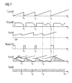
- Fig. 7 shows signal diagrams illustrating the operation of the method and apparatus 1 according to the present invention.
- Fig. 7 shows the operation period time T, the drain voltage V drain at the drain terminal D, the set voltage V set output by the peak current correction control circuit 17, the voltage at the drain gate terminal G of the charging/discharging transistor 9, the current I coil through the primary coil 5 and the resulting average current I avg .
- the set voltage V set is the internal reference voltage which sets the maximal peak current I peak .
- the maximal peak current I peak is V set R sns .
- the compensation feed forward slope is started. In this way, the slope compensation does correct for the time that the new charge cycle is started (valley detection) and for the charging time (V HV variation). This results in an almost constant average current I avg , as shown in Fig. 7 .
- I set 1 3 ⁇ I max ⁇ 1 + 2 ⁇ T T max
- I avg 1 3 ⁇ 1 + 2 ⁇ T T max 2 ⁇ I max 8 ⁇ T max T
- the following Table indicates different scenarios, i.e. a first scenario with an ideal slope compensation as defined by the equations, a scenario with a linear compensation as defined by the equations and a scenario with no compensation.
- Fig. 8 shows the dependency between a ratio between the average current I avg and the peak current I peak and a ratio between the period time T and the maximum period time T max for the different three scenarios as indicated in the Table, i.e. ideal compensation (I), linear compensation (II) and no compensation (III).
- IAVGideal error Iset I ⁇ max IAVG I ⁇ max IAVGno comp .
- Fig. 9 shows the dependency between the ratio between the set current I set and the maximum peak current I peak and the ratio between the period time T and the maximum period time T max for the three scenarios, as given in the above Table, i.e. ideal compensation (I), linear compensation (II) and no compensation (III).
- a square root compensation for the maximum peak current I peak can keep the average current I avg flowing through the LED I avg constant for a fast variation of the supply voltage V HV and valley hopping created in the QR mode.
- Implementing a straight forward linear compensation for the peak current I peak reduces the error in the average LED current I avg for a fast variation of the period time to less than 11.1%, as can also be seen in the above Table.
- Optimizing the rise time of the slope, the variation of the average current I avg can be reduced to less than 6%.
- a correction system for a voltage output QR flyback converter.
- the correction system does also reduce the dependency of the output voltage (sensitivity) on the input voltage variation of the supply voltage V HV .
Landscapes
- Circuit Arrangement For Electric Light Sources In General (AREA)
Abstract
Description
- The invention relates to a method and an apparatus for stabilizing an average current of at least one LED lamp within a flyback converter and in particular to a flyback light-emitting diode driver for stabilizing an average current flowing through at least one LED lamp.
- Light-emitting diode (LED) lamps are rapidly replacing conventional incandescent lamps, fluorescent lamps and other types of light sources due to its high efficiency, high reliability, small size and long operation lifetime. The brightness of the LED lamp depends on the average current that flows through the LED lamp. Consequently, there is a need for a method and apparatus for stabilizing an average current flowing through the LED lamp.
- To improve the safety of LED lamps, mostly a mains isolated topology is used, where the peak current is controlled by a circuitry with a flyback topology. The flyback topology allows the LED driver to operate at a larger input voltage range which makes it suitable to connect the LED driver directly to a rectified mains input voltage. Providing a Quasi Resonance operation of the flyback LED driver increases the efficiency of the LED driver. Moreover, a flyback light-emitting diode driver has low manufacturing costs due to a relatively simple current detection, a simple mains isolated casing and lower EMI power due to simpler input filters.
- However, a problem of a light-emitting diode driver comprising a Q R flyback topology is that its operation frequency can vary abruptly and can create an overshoot in the LED current flowing through the LED lamp of more than 400%.
- Accordingly, it is an object of the present invention to provide an apparatus and a method to overcome these drawbacks.
- Accordingly, the invention provides according to a first aspect of the present invention a flyback light-emitting diode driver for stabilizing an average current flowing through at least one LED lamp comprising the features of
claim 1. - Accordingly, the invention provides a flyback light-emitting diode driver for stabilizing an average current flowing through at least one LED lamp, said flyback LED driver comprising
a peak current correction control circuit adapted to compensate dynamically a variation of an operation time period of said flyback LED driver by adjusting a peak current of a coil connected in parallel with the at least one LED lamp in response to the changing operation time period. - Accordingly, the flyback light-emitting diode driver accord-ing to the first aspect of the present invention has the advantage that it does reduce overshoot currents flowing through the LED lamp.
- In a possible embodiment of the flyback LED driver according to the first aspect of the present invention a charging/discharging transistor is connected to the coil and is adapted to charge the coil when the charging/discharging transistor is turned on and to discharge the coil through the at least one LED lamp when the charging/discharging transistor is turned off.
- In a still further possible embodiment of the flyback LED driver according to the first aspect of the present invention, the charging/discharging transistor is a NMOS transistor having a gate terminal controlled by the peak current correction control circuit, a drain terminal connected to said coil, and a source terminal connected via a sense resistor to ground.
- In a still further possible embodiment of the flyback LED driver according to the first aspect of the present invention, the coil is a primary coil of a transformer, wherein a supply voltage is applied to a first terminal of the coil and a second terminal of the coil is connected via a flyback diode to the at least one LED lamp and is connected to the drain terminal of the charging/discharging NMOS transistor.
- In a still further possible embodiment of the flyback LED driver according to the first aspect of the present invention, the transformer comprises a secondary coil connected to a first detection circuit adapted to detect a time when the primary coil of the transformer is discharged and to generate a corresponding first trigger signal applied to the peak current correction control circuit to start the compensation of the variation of the operation time period.
- In a still further possible embodiment of the flyback LED driver according to the first aspect of the present invention, the secondary coil of the transformer is connected to a second detection circuit adapted to detect a time when a ringing amplitude of a drain voltage at the drain terminal of the charging/discharging NMOS transistor reaches a minimum value and to generate a corresponding second trigger signal to turn the NMOS charging/discharging transistor on such that the primary coil of the transformer is discharged.
- In a still further possible embodiment of the flyback LED driver according to the first aspect of the present invention, the peak current correction control circuit outputs an adjustable set voltage which is compared by a comparator circuit with a voltage across the sense resistor connected to the source terminal of the charging/discharging NMOS transistor.
- In a still further possible embodiment of the flyback LED driver according to the first aspect of the present invention, if the comparator circuit detects that the voltage across the sense resistor reaches the set voltage, output by the peak current correction control circuit, it generates a reset control signal to turn off the charging/discharging NMOS transistor such that the primary coil of the transformer is discharged through the at least one LED lamp.
- In a still further possible embodiment of the flyback LED driver according to the first aspect of the present invention, the operation time period of the flyback LED driver comprises
a first charging time phase during which the coil is charged until the charging/discharging transistor is turned off by the comparator circuit,
a second flyback time phase during which the coil is discharged through the at least one LED lamp with the charging/discharging transistor being turned off, and a third time phase until the charging/discharging transistor is turned on again in response to the second trigger signal generated by the second detection circuit. - In a still further possible embodiment of the flyback LED driver according to the first aspect of the present invention, the operation time period of the flyback LED driver is given by:

- wherein Δt1 is the first charging time phase,
- Δt2 is the second flyback time phase, and
- Δt3 is the third time phase.
- In a possible embodiment of the flyback LED driver according to the first aspect of the present invention, the first charging time phase Δt1 is given by:

- wherein Ipeak is the peak current flowing through the coil, L1 is the inductivity of the coil,
- VHV is the supply voltage applied to the first terminal of the coil.
- In a further possible embodiment of the flyback LED driver according to the first aspect of the present invention, the second flyback time phase Δt2 is given by

- Ipeak is the peak current flowing through the coil,
- L1 is the inductivity of the coil, and
- VLED is the forward voltage of the at least one LED lamp.
- In a further possible embodiment of the flyback LED driver according to the first aspect of the present invention, the third time phase Δt3 is given by:

wherein TOSC is the oscillation time period of the ringing drain voltage at the drain terminal of the charging/discharging transistor. - In a still further possible embodiment of the flyback LED driver according to the first aspect of the present invention, the average current Iavg flowing through the at least one LED lamp depends on the peak current of the coil and the second flyback time phase,
wherein the average current Iavg is given by:
wherein the peak current correction control circuit is configured to compensate dynamically in real time a variation of the operation time period T by adjusting the peak current Ipeak of the coil. - In a still further possible embodiment of the flyback LED driver according to the first aspect of the present invention, the peak current control circuit is configured to adjust the peak current by adapting the amplitude of the output set voltage Vset depending on a ratio between the second flyback Δt2 time phase and the operation time period T.
- In a still further possible embodiment of the flyback LED driver according to the first aspect of the present invention, the peak current control circuit is configured to increase the set voltage Vset when the ratio between the second flyback time phase Δt2 and the operation time period T decreases.
- In a still further possible embodiment of the flyback LED driver according to the first aspect of the present invention, the gate terminal of the charging/discharging NMOS transistor is connected to an output of a control flip-flop set in response to a set control signal and reset in response to the reset control signal generated by the comparator circuit.
- In a still further possible embodiment of the flyback LED driver according to the first aspect of the present invention, the set control signal is generated by a logic circuit during an operation time window between a predetermined minimum time period Tmin and a predetermined maximum time period Tmax in response to the second trigger signal generated by the second detection circuit.
- In a still further possible embodiment of the flyback LED driver according to the first aspect of the present invention, the peak current correction control circuit is configured to perform a linear slope compensation, wherein the set voltage Vset is increased linear over time.
- In a still further possible embodiment of the flyback LED driver according to the first aspect of the present invention, the peak current correction control circuit is configured to adjust the set voltage Vset in a linear slope over time in response to the first trigger signal generated by the first detection circuit.
- The invention further provides a method for stabilizing an average current of at least one LED lamp within a flyback converter comprising the features of claim 18.
- Accordingly, the invention provides according to a second aspect a method for stabilizing an average current of at least one LED lamp within a flyback converter,
wherein a variation of an operation time of the flyback converter is compensated dynamically in real time by increasing a peak current of a coil connected in parallel with the at least one LED lamp in response to the changing operation time period. - According to a possible embodiment of the method according to the second aspect of the present invention, an electrical current flowing through the coil is measured and the compensation is started when the electrical current of the coil discharged through the LED lamp becomes zero.
- The invention further provides according to a third aspect an LED lamp having the features of
claim 20. - Accordingly, the invention provides according to the third aspect an LED lamp comprising a flyback LED driver for stabilizing an average current flowing through the LED lamp, said flyback LED driver having a peak current correction control circuit adapted to compensate dynamically a variation of an operation time period of the flyback LED driver by adjusting a peak current of a coil connected in parallel with the LED lamp in response to the changing operation time period.
- In the following, possible embodiments of different aspects of the present invention are described in more detail with reference to the enclosed figures.
- Fig. 1
- shows a circuit diagram of an exemplary embodiment of a flyback light-emitting diode driver according to the first aspect of the present invention;
- Fig. 2
- shows signal diagrams for illustrating the operation of a flyback light-emitting diode driver;
- Fig. 3
- shows the dependency of an average current flowing through an LED lamp on a period time variation to illustrate the operation of the apparatus and method according to the present invention;
- Fig. 4
- illustrates an approximation of a peak current with a linear slope depending on the period time as employed in a possible embodiment of the flyback light-emitting diode driver according to the present invention;
- Fig. 5
- shows a diagram for illustrating a dependency of an adjustable set voltage to the period time to illustrate the operation of the method and apparatus according to the present invention;
- Fig. 6
- shows signal diagrams illustrating the operation of a possible embodiment of an apparatus and method according to the present invention;
- Fig. 7
- shows further signal diagrams for illustrating the operation of a method and apparatus according to the present invention;
- Fig. 8
- shows a diagram illustrating the ratio between the average current and the peak current depending on a ratio between a period time and a maximum period time for different scenarios for illustrating the operation of a method and apparatus according to the present invention;
- Fig. 9
- shows a diagram illustrating the ratio between a set current and a peak current depending on a ratio between a period time and a maximum period time for different scenarios for illustrating the operation of an apparatus and method according to the present invention.
-
Fig. 1 shows a specific exemplary embodiment of a flyback light-emitting diode (LED)driver 1 for stabilizing an average current Iavg flowing through at least one LED lamp. The flyback light-emittingdiode driver circuit 1, as illustrated inFig. 1 is connected to one or more LED lamps 2-1, 2-2, ... 2-n, as shown inFig. 1 . The numbers of LED lamps 2-i connected in series can vary. As can be seen inFig. 1 , a capacitor 3 is connected in parallel to the LED lamps 2-i. The driver is supplied with a supply voltage VHV provided by asupply voltage source 4. The flyback light-emittingdiode driver 1 as shown inFig. 1 is adapted to stabilize an average current Iavg flowing through the at least one LED lamp 2-i. Theflyback LED driver 1 comprises a coil 5 which is connected in parallel with the at least one LED lamp 2-i, as illustrated inFig. 1 . The coil 5 comprises a first terminal to which the supply voltage VHV is applied. The coil 5 further comprises a second terminal which is connected via a flyback diode 6 to the LED lamps 2-i. In the shown embodiment ofFig. 1 , the coil 5 forms a primary coil of a transformer 7 comprising the primary coil 5 and asecondary coil 8. - In the flyback
LED driver circuit 1 as illustrated inFig. 1 , a charging/dischargingtransistor 9 is provided. In the exemplary embodiment shown inFig. 1 , the charging/dischargingtransistor 9 is a NMOS transistor comprising a gate terminal G, a drain terminal D and a source terminal S. As can be seen inFig. 1 , the drain terminal D of the charging/dischargingtransistor 9 is connected to the second terminal of the primary coil 5 and the flyback diode 6 at a circuit node 10. The charging/dischargingtransistor 9 being connected to the coil 5 is adapted to charge the coil 5 when the charging/dischargingtransistor 9 is turned on and to discharge the coil 5 to the at least one LED lamp 2-i when the charging/dischargingtransistor 9 is turned off. As can be seen inFig. 1 , the source terminal S of the charging/dischargingtransistor 9 is connected via asense resistor 11 to ground GND. The flyback light-emittingdiode driver 1 comprises a peak current correction control circuit which is adapted to compensate dynamically a variation of an operation time period T of theflyback LED driver 1 by adjusting a peak current Ipeak of the coil 5 connected in parallel with the at least one LED lamp 2-i to response to the changing operation time period T. - The
secondary coil 8 of the transformer 7 is connected via asignal line 12 to avoltage dividing circuit 13 comprising afirst resistor 14 and a second resistor 15 to afirst detection circuit 16. Thefirst detection circuit 16 is adapted to detect a time tz when the primary coil 5 of the transformer 7 is discharged and generates a corresponding first trigger signal TS1 applied to the peak current correction control circuit 17 to start a compensation of a variation of the operation time period T. Thesecondary coil 8 of the transformer 7 is further connected via thesignal line 12 and thevoltage dividing circuit 13 to a second detection circuit 18 adapted to detect a time tv when a ringing amplitude of a drain voltage VD at the drain terminal D and the node 10 reaches a minimum value to generate a corresponding second trigger signal TS2 to turn the NMOS charging/dischargingtransistor 9 directly or indirectly on such that the primary coil 5 of the transformer 7 is charged. - The peak current correction control circuit 17 receiving the first trigger signal TS1 starts the compensation of the variation of the operation time period T to output an adjustable set voltage Vset which is compared by a
comparator circuit 19 with a voltage across thesense resistor 11 connected to the source terminal S of the charging/dischargingNMOS transistor 9. In the shown exemplary embodiment ofFig. 1 , thecomparator circuit 19 is formed by an operation amplifier having a non-inverted input connected via aline 20 to acircuit node 21 between the source terminal S of the charging/dischargingtransistor 9 and thesense resistor 11. The inverting input of theoperation amplifier 19 receives the adjustable set voltage Vset from the peak current correction control circuit 17. If thecomparator circuit 19 detects that the voltage across thesense resistor 11 reaches the set voltage Vset output by the peak current correction control circuit 17, thecomparator circuit 19 generates a reset control signal R applied to an RS flip-flop 22 to turn off the charging/dischargingNMOS transistor 9 such that the primary coil 5 of the transformer 7 is discharged through the at least one LED lamp 2-i. The RS flip-flop 22 comprises a data output Q connected via acontrol signal line 23 to the gate terminal G of the charging/ dischargingNMOS transistor 9. - The RS flip-
flop 22 comprises a set input S which receives a logical control signal ON_NMOST viasignal line 24 to turn the charging/dischargingtransistor 9 on wherein the control signal is generated directly or indirectly by the second trigger signal TS2 output by the second detection circuit 18. - The operation time period T of the
flyback LED driver 1 does comprise different phases. The operation time period T comprises a first charging time period Δt1 during which the coil 5 is charged until the charging/dischargingtransistor 9 is turned off by thecomparator circuit 19. The operation time period T further comprises a second flyback time phase Δt2 during which the coil 5 is discharged through the at least one LED lamp 2-i with the charging/dischargingtransistor 9 being turned off. The operation time period T further comprises a third time phase Δt3 until the charging/dischargingtransistor 9 is turned on again in response to the second trigger signal TS2 generated by the second detection circuit 18. - Accordingly, the operation time period T of the flyback LED driver is given by:

- wherein Δt1 is the first charging time phase,
- Δt2 is the second flyback time phase, and
- Δt3 is the third time phase.
- In a possible embodiment, the first charging time phase Δt1 is given by:

- wherein Ipeak is the peak current flowing through the coil 5,
- and L1 is the inductivity of the coil 5 and VHV is the supply voltage generated by the
supply voltage source 4 and applied to the first terminal of the coil 5. - The second flyback time phase Δt2 of the operation time period T is given in a possible embodiment by:

- wherein Ipeak is the peak electrical current flowing through the coil 5,
- L1 is the inductivity of the coil 5, and
- VLED is the forward voltage of the at least one LED lamp 2-i.
- Further, the third time phase Δt3 of the operation time period T is given by:

wherein TOSC is the oscillation time period of a ringing drain voltage VD at the drain terminal D of the charging/dischargingtransistor 9. - The average current Iavg flowing through the at least one LED lamp depends on the peak current Ipeak of the coil 5 and the second flyback time phase Δt2, wherein the average current Iavg is given by:

- The peak current correction control circuit 17 is configured to compensate dynamically in real time a variation of the operation time period (T) by adjusting the peak current Ipeak of the coil 5. The peak current control circuit 17 is configured in a possible embodiment to adjust the peak current Ipeak by adapting the amplitude of the output set voltage Vset applied to the
comparator circuit 19 depending on a ratio between the second flyback time phase Δt2 and the operation time period T. The peak current control circuit 17 is configured to increase the set voltage Vset when the ratio between the second flyback time phase Δt2 and the operation time period T does decrease. - As shown in
Fig. 1 , the gate terminal G of the charging/dischargingNMOS transistor 9 is connected to the output Q of the control flip-flop 22 set in response to a set control signal S and reset in response to the reset control signal R generated by thecomparator circuit 19. The set control signal S is generated by alogic circuit 25 during an operation time window between a predetermined minimum time period Tmin and a predetermined maximum time period Tmax in response to the second trigger signal TS2 generated by the second detection circuit 18.Fig. 1 shows a specific exemplary embodiment of thelogic circuit 25 generating the set control signal S applied via thecontrol line 24 to the set input of the RS flip-flop 22 in response to the second trigger signal TS2 generated by the second detection circuit 18. - The peak current correction control circuit 17 is configured in a possible embodiment to perform a linear slope compensation, wherein the set voltage Vset output by the peak current correction control circuit 17 via a
signal control line 26 is increased linear over time. The peak current correction control circuit 17 is configured to adjust the set voltage Vset in a linear slope over time in response to the first trigger signal TS1 generated by thefirst detection circuit 16. - The flyback light-emitting
diode driver 1 as illustrated inFig. 1 provides a real time dynamic peak current control to suppress LED current variation created through supply voltage variation and so-called valley hopping. Real time peak current correction provided by the real time correction control circuit 17 is performed through adding a periodic rising slope of the set voltage. The linear implementation of the slope correction curve can reduce the overshoot error of the overshooting LED current from more than 300% back to less than 11%. In a possible embodiment, the flyback light-emittingdriver circuit 1 as illustrated inFig. 1 can be integrated in an LED lamp. - The real time dynamic peak current correction control for the QR flyback LED driver system provides a more stable QR operation and does suppress automatically a LED current variation caused by supply voltage variation and valley hopping. With the real time dynamic peak current correction control it is possible to provide a more accurate LED current dimming. Accordingly, the
circuit 1 as illustrated inFig. 1 provides a real time current correction for the QR flyback peak current system. As a key benefit it does suppress LED current variations due to input voltage variations suppresses LED current variations due to valley hopping in the QR mode and makes it possible to provide a stable LED dimming for a QR flyback peak current system. - In a flyback DC-DC converter system, the coil current, i.e. the current flowing through the coil 5, is charged to a predetermined value i.e. the peak current Ipeak. The charging/discharging
transistor 9 is turned on until the voltage across thesense resistor 11 reaches a preset voltage. The voltage across the coil 5 approximates the supply voltage VHV. When the predetermined peak current value Ipeak is reached, the charging/dischargingtransistor 9 is turned off and the coil 5 is discharged through the LED lamp 2-i. The voltage across the coil 5 is approximately the forward voltage of the LED lamp and the drain voltage VD is pushed to VHV + VLED. - After the coil 5 has been discharged, a damped oscillation voltage at the drain terminal D of the charging/discharging
transistor 9 occurs having an initial amplitude of the LED forward voltage VLED and an oscillation frequency f depending mainly on the inductivity L of the coil 5 and the drain source capacitance CDS of the charging/dischargingtransistor 9. The next cycle is started when the drain voltage VD reaches the lowest value during the oscillation phase. This does reduce switching losses in the charging/dischargingtransistor 9 and reduces EMI. The system does operate in a Quasi-Resonance QR mode. - The operation time period T is inversely proportional to the switching frequency f of the QR system and does depend on the charging time of the coil 5, the discharging time of the coil 5 and on the time until the lowest value of the ringing is detected by the second detection circuit 18.
- Accordingly, the operation time period T of the
flyback LED driver 1 is the sum of the first charging time phase Δt1 during which the coil 5 is charged until the charging/dischargingtransistor 9 is turned off by thecomparator circuit 19, a second flyback time phase Δt2 during which the coil 5 is discharged through the at least one LED lamp 2-i with the charging/dischargingtransistor 9 being turned off and a third time phase Δt3 until the charging/dischargingtransistor 9 is turned on again in response to the second trigger signal TS2 generated by the second detection circuit 18. The average current Iavg flowing through the LED-lamp 2-i in, the QR resonant flyback DC-DC system depends on the flyback time phase Δt2 and the operation time period T:
- Accordingly, the average current Iavg flowing through the LED lamp depends on the supply voltage VHV, the forward voltage VLED, the peak current Ipeak, the oscillation time period Tosc and the inductivity L of the coil 5.
- The forward voltage VLED of the LED lamp 2-i depends on the temperature and on the manufacturing lot of the LED lamp. An error in the inductivity L of the coil 5 depends mainly on the manufacturing lot. The variation of the oscillation time period Tosc depends on the inductivity value L and parasitic capacitances of the charging/discharging
transistor 9, the printed circuit board PCB and decoupling capacitors. All the parameters are static errors and can be compensated by an adjusting correction mechanism in the controlling device. The high supply voltage VHV applied to the coil 5 can comprise a large variation. -
Fig. 2 shows signal diagrams for illustrating the drain voltage Vdrain at the drain terminal D of the charging/dischargingtransistor 9 and the corresponding current flowing through the coil 5 over time. As can be seen inFig. 2 , the operation time period T of theflyback LED driver 1 comprises three phases, i.e. a first charging time phase, where the current flowing through the coil 5 increases until it reaches a peak current Ipeak, a second time phase, where the coil 5 is discharged and the current flowing through the coil 5 is going down and a third time phase, where the voltage VD at the drain terminal D and the current is oscillating with an oscillation frequency fosc. - Fast changes can create larger variations on the average LED current Iavg. The current overshoot of the LED current can lead to a lifetime reduction and even to a destruction of the LED lamp. A change of factor two in the operation period time T does change directly the average current Iavg with a factor of two. To compensate the average current Iavg for the dynamic change created through valley hopping and jumps of the supply voltage VHV, the peak current correction circuit 17 performs a real time compensation or correction.
-
Fig. 3 illustrates the dependency of the average current Iavg from variations of the operation period time T.Fig. 3 shows the current flowing through the coil Icoil depending on the operation period time T. - If the flyback converter is set to a predetermined operation frequency


or
- When the operation period time T changes, the average current Iavg does change as well. To keep the average current Iavg constant, the maximum or peak current can also be changed. For instance, for T2 = T/4:

- The change of the peak current Ipeak can be approximated by a linear slope, wherein the linear slope depends on the period time T, as also illustrated in
Fig. 4 . The flyback time phase depends on the inductivity L of the coil 5 and the forward voltage VLED. - When the charging/discharging
transistor 9 is turned on, the positive supply voltage VHV is set across the primary coil 5 of the transformer 7 and generates a charge current


wherein Rsns is the resistance of thesense resistor 11. - If the preset peak current value Ipeak is reached, the charging/discharging
transistor 9 is turned off and the coil current Icoil flowing through the coil 5 is discharged through the LED lamp 2-i. The discharge current is given by:
- This does create a negative voltage across the primary coil 5 (Vdiode + VLED ) and a positive voltage

secondary coil 8 of the transformer 7. The drain voltage VD is pushed to: VHV + VLED + Vdiode. - After the coil 5 has been discharged, a damped oscillation voltage on the drain terminal D of the charging/discharging
transistor 9 occurs. The flyback diode 6 stops conducting and the drain voltage VD does jump from VHV + VLED + Vdiode to VHV. This does induce a ringing with an initial amplitude of VLED and with an oscillation frequency fosc depending mainly on the inductivity L1 of the coil 5 and the drain source capacitance CDS of the charging/dischargingtransistor 9. - The signal Vsec to the secondary side at the
secondary coil 8 of the transformer 7 is applied to the second detection circuit 18 adapted to detect the signal valley. The second detection circuit 18 generates a signal pulse, i.e. a trigger signal TS2, when the ringing amplitude reaches its minimum value. This triggers to start the next cycle charging the coil 5 with an increasing current when the drain voltage VD reaches the lowest value during the oscillation phase. Starting the next cycle of the converter at the lowest drain voltage VD is also called Quasi Resonance operation mode. - To ensure a correct operation, the next cycle is started after a predefined maximum time Tmax which defines the lowest switching frequency. To limit the maximal frequency and preventing a false trigger which can be caused by a switching noise, a minimum switching time Tmin is defined, where the trigger signal TS2 generated by the second detection circuit 18 is ignored. Accordingly, an operation time window is provided between the predetermined minimum time period Tmin and the predetermined maximum time period Tmax in response to the second trigger signal TS2 generated by the second detection circuit 18. The used QR flyback in the operation time window can be set for instance between 1/4T and T, creating the condition for the NMOST control signal as follows: SWset = {tvalley AND (T>1/4T)} OR Tmax ·
- In the QR flyback system, the average LED current Iavg is the average flyback current.

- In the QR flyback system, the ratio

- To keep the average current Iavg constant, the amplitude of the set voltage Vset (Ipeak ·Rsns ) value is adapted. The set voltage value Vset is increased when the ratio

- The optimum adapted set voltage Vset is a square root function. The set voltage Vset function can be approximated with a first order function, as also illustrated in
Fig. 5 . - In a possible embodiment, the maximum value of the set voltage Vset can be chosen to be 1.4V. Further, the second correction point can be chosen at 0.5·V setmax. This results in a flyback time tflyback of 1/8Tmax and a period time of 1/4Tmax.

- If Iavg2 = Iavg1, this results in that T2 = 1/4Tmax.
- This results in a linear slope approximation:


- The
first detection circuit 16 creates a signal TS1 to indicate the moment in time, where the primary coil 5 is discharged. Thefirst detection circuit 16 is adapted to detect the time tz when the primary coil 5 of the transformer 7 is discharged and does generate a corresponding first trigger signal TS1 applied to the peak current correction control circuit 17 to start the compensation of the variation of the operation time period T. Accordingly, the compensation of the set voltage Vset is triggered by thefirst detection circuit 16. - The time base for the slope compensation is synchronized at a maximum period of the QR resonance system. Using the same DC reference current for the slope compensation as that of the maximal period timer, the
logic circuit 25 does make the slope compensation independently of the frequency setting.

- As can be seen in
Fig. 1 , thelogic circuit 25 implements the operation time window between the minimum period time Tmin and the maximum period time Tmax. As can be seen inFig. 1 , the trigger signal TS2 generated by the second detection circuit 18 is applied to an ANDgate 25A being connected also to the output of acomparator 25B implemented as an operation amplifier. The output of the ANDgate 25A is applied to anOR gate 25C having a second input connected to anothercomparator 25D also implemented as an operation amplifier, as illustrated inFig. 1 . The output of theOR gate 25C is connected to a set input of a RS flip-flop 25E having an output Q being connected via thecontrol line 24 to the set input of the RS flip-flop 22 and providing the On_NMOST control signal to turn on the charging/dischargingtransistor 9. The data output Q of the flip-flop 25E is fed back via adelay circuit 25F to the reset input R of the same flip-flop. The output Q of the flip-flop 25E controls aswitch 25G connected to acapacitor 25H having the capacitance Ctimer. Thelogic circuit 25 further comprises a current source 25I providing a current Iosc and areference voltage source 25J generating a voltage VTmax. - Using a QR time window with a maximum frequency of 1/4T, the beginning part of the slope can be a straight line. This can be achieved by using a offset voltage Voffset of 0.5Vsetmax and a minimum set voltage V setmin with 0.5·V setmax, as also illustrated in
Fig. 5 .Voffset VSETmin VSETmax Vslope(Tmax) VTMAX Cslope 

[V] [V] [V] [V] [V] 0 0.56 1.4 1.68 1.2 0.714·CTIMER 0.14 0.7 1.4 1.68 1.2 0.714·CTIMER Remark: Voffset=0.14V, slope starts with a straight line at tz. - The value of the slope voltage Vslope can be reset after detection of the peak current Ipeak, when the charging/discharging
transistor 9 is turned off. The slope has to be ready for the next detection of the time tz so that the reset time depends on the discharging time of the primary coil 5. -
Fig. 6 illustrates the timing of different signals within thedriver circuit 1, in particular the drain voltage Vdrain at the drain terminal of the charging/dischargingtransistor 9, the coil current Icoil flowing through the primary coil 5. The secondary voltage Vsec of thesecondary coil 8, the set voltage Vset output by the peak current correction control circuit 17 and the control signal SW are applied to the gate terminal of the charging/dischargingtransistor 9. - To compensate the influence of the variable period time T of the average current Iavg, the maximum reference current is increased depending on the period time T.
-
Fig. 7 shows signal diagrams illustrating the operation of the method andapparatus 1 according to the present invention.Fig. 7 shows the operation period time T, the drain voltage Vdrain at the drain terminal D, the set voltage Vset output by the peak current correction control circuit 17, the voltage at the drain gate terminal G of the charging/dischargingtransistor 9, the current Icoil through the primary coil 5 and the resulting average current Iavg. The set voltage Vset is the internal reference voltage which sets the maximal peak current Ipeak. The maximal peak current Ipeak is
Fig. 7 . - A small error might be created by using a straight line slope compensation instead of a square root compensation. For the chosen slope compensation, the average current Iavg can be calculated depending on current period time T.
With condition:
and
- For an ideal slope compensation, the electrical currents I are given as follows:


- For a linear slope compensation, the electrical currents I are given by:


- The following Table indicates different scenarios, i.e. a first scenario with an ideal slope compensation as defined by the equations, a scenario with a linear compensation as defined by the equations and a scenario with no compensation.
-
Fig. 8 shows the dependency between a ratio between the average current Iavg and the peak current Ipeak and a ratio between the period time T and the maximum period time Tmax for the different three scenarios as indicated in the Table, i.e. ideal compensation (I), linear compensation (II) and no compensation (III).Ideal linear compensation no compensation 

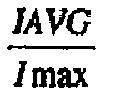


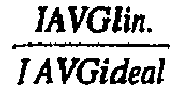
error 


error 0.2 0.447 0.125 0.467 0.136 1.09 8.9% 1 0.625 5.00 400.0% 0.25 0.500 0.125 0.500 0.125 1.00 0.0% 1 0.500 4.00 300.0% 0.3 0.548 0.125 0.533 0.119 0.95 -5.2% 1 0.417 3.33 233.3% 0.35 0.592 0.125 0.567 0.115 0.92 -8.396 1 0.357 2.86 185.7% 0.4 0.632 0.125 0.600 0.113 0.90 -10.0% 1 0.313 2.50 150.0% 0.45 0.671 0.125 0.633 0.111 0.89 -10.9% 1 0.278 2.22 122.2% 0.46 0.678 0.125 0.640 0.111 0.89 -11.0% 1 0.272 2.17 117.4% 0.48 0.693 0.125 0.653 0.111 0.89 -11.1% 1 0.260 2.08 108.3% 0.49 0.700 0.125 0.660 0.111 0.89 -11.1% 1 0.255 2.04 104.1% 0.5 0.707 0.125 0.667 0.111 0.89 -11.1% 1 0.250 2.00 100.0% 0.51 0.714 0.125 0.673 0.111 0.89 -11.1% 1 0.245 1.96 96.1% 0.52 0.721 0.125 0.680 0.111 0.89 -11.1% 1 0.240 1.92 92.3% 0.54 0.735 0.125 0.693 0.111 0.89 -11.0% 1 0.231 1.85 85.2% 0.56 0.748 0.125 0.707 0.111 0.89 -10.8% 1 0.223 1.79 78.6% 0.58 0.762 0.125 0.720 0.112 0.89 -10.6% 1 0.216 1.72 72.4% 0.6 0.775 0.125 0.733 0.112 0.90 -10.4% 1 0.208 1.67 66.7% 0.6 0.775 0.125 0.733 0.112 0.90 -10.4% 1 0.208 1.67 66.7% 0.65 0.806 0.125 0.767 0.113 0.90 -9.6% 1 0.192 1.54 53.8% 0.7 0.837 0.125 0.800 0.114 0.91 -8.6% 1 0.179 1.43 42.9% 0.75 0.866 0.125 0.833 0.116 0.93 -7.4% 1 0.167 1.33 33.3% 0.8 0.894 0.125 0.867 0.117 0.94 -6.1% 1 0.156 1.25 25.0% 0.85 0.922 0.125 0.900 0.119 0.95 -4.7% 1 0.147 1.18 17.6% 0.9 0.949 0.125 0.933 0.121 0.97 -3.2% 1 0.139 1.11 11.1% 0.95 0.975 0.125 0.967 0.123 0.98 -1.6% 1 0.132 1.05 5.3% 1 1.000 0.125 1.000 0.125 1.00 0.0% 1 0.125 1.00 0.0% - Further,
Fig. 9 shows the dependency between the ratio between the set current Iset and the maximum peak current Ipeak and the ratio between the period time T and the maximum period time Tmax for the three scenarios, as given in the above Table, i.e. ideal compensation (I), linear compensation (II) and no compensation (III). - As can be seen, a square root compensation for the maximum peak current Ipeak can keep the average current Iavg flowing through the LED Iavg constant for a fast variation of the supply voltage VHV and valley hopping created in the QR mode. Implementing a straight forward linear compensation for the peak current Ipeak, reduces the error in the average LED current Iavg for a fast variation of the period time to less than 11.1%, as can also be seen in the above Table. Optimizing the rise time of the slope, the variation of the average current Iavg can be reduced to less than 6%.
- According to a further aspect of the invention, a correction system is provided for a voltage output QR flyback converter. The correction system does also reduce the dependency of the output voltage (sensitivity) on the input voltage variation of the supply voltage VHV.
Claims (20)
- A flyback light-emitting diode (LED) driver (1) for stabilizing an average current (Iavg) flowing through at least one LED lamp (2-i),
said flyback LED driver (1) comprising
a peak current correction control circuit (17) adapted to compensate dynamically a variation of an operation time period (T) of said flyback LED driver (1) by adjusting a peak current (Ipeak) of a coil (5) connected in parallel with at least one LED lamp (2-i) in response to the changing operation time period (T). - The flyback LED driver according to claim 1,
wherein a charging/discharging transistor (9) is connected to said coil (5) and is adapted to charge the coil (5) when the charging/discharging transistor (9) is turned on and to discharge the coil (5) through the at least one LED lamp (2-i) when the charging/discharging transistor (9) is turned off. - The flyback LED driver according to claim 2,
wherein the charging/discharging transistor (9) is a NMOS transistor having a gate terminal (G) controlled by said peak current correction control circuit (17), a drain terminal (D) connected to said coil (5), and a source terminal (S) connected via a sense resistor (11) to ground (GND). - The flyback LED driver according to claim 3,
wherein the coil (5) is a primary coil of a transformer (7), wherein a supply voltage (VHV) is applied to a first terminal of said coil (5) and a second terminal of said coil (5) is connected via a flyback diode (6) to said at least one LED lamp (2-i) and is connected to the drain terminal (D) of said charging/discharging NMOS transistor (9). - The flyback LED driver according to claim 4,
wherein the transformer (7) comprises a secondary coil (5) connected to a first detection circuit (16) adapted to detect a time (tz) when the primary coil (5) of said transformer (7) is discharged and to generate a corresponding first trigger signal (TS1) applied to said peak current correction control circuit (17) to start the compensation of the variation of said operation time period (T). - The flyback LED driver according to claim 5,
wherein the secondary coil (8) of said transformer (7) is connected to a second detection circuit (18) adapted to detect a time (tv) when a ringing amplitude of a drain voltage (VD) at the drain terminal (D) of said charging/discharging NMOS transistor (9) reaches a minimum value and to generate a corresponding second trigger signal (TS2) to turn the NMOS charging/discharging transistor (9) on such that the primary coil (5) of said transformer (7) is discharged. - The flyback LED driver according to one of the preceding claims 3 to 6,
wherein the peak current correction control circuit (17) outputs an adjustable set voltage (Vset) which is compared by a comparator circuit (19) with a voltage across the sense resistor (11) connected to the source terminal (S) of said charging/discharging NMOS transistor (9). - The flyback LED driver according to claim 7,
wherein if the comparator circuit (19) detects that the voltage across the sense resistor (11) reaches the set voltage (Vset), output by said peak current correction control circuit (17), it generates a reset control signal (R) to turn off the charging/discharging NMOS transistor (9) such that the primary coil (5) of said transformer (7) is discharged through the at least one LED lamp (2-i). - The flyback LED driver according to one of the preceding claims 6 to 8,
wherein the operation time period (T) of said flyback LED driver (1) comprises:- a first charging time phase (Δt1) during which the coil (5) is charged until the charging/discharging transistor (9) is turned off by said comparator circuit (19),- a second flyback time phase (Δt2) during which the coil (L1) is discharged through the at least one LED lamp (2-i) with the charging/discharging transistor (9) being turned off, and- a third time phase (Δt3) until the charging/discharging transistor (9) is turned on again in response to the second trigger signal (TS2) generated by the second detection circuit (18). - The flyback LED driver according to claim 9,
wherein the operation time period (T) of said flyback LED driver (1) is given by:
wherein
Δ t1 is the first charging time phase given by: Ipeak being the peak current flowing through the coil (5),L1 being the inductivity of the coil (5),VHV being the supply voltage applied to the first terminal of the coil (5),wherein Δt2 is the second flyback time phase given by:
 Ipeak being the peak current flowing through the coil (5),L1 being the inductivity of the coil (5), andVLED being the forward voltage of the at least one LED lamp (2-i), andwherein Δt3 is the third time phase given by:
TOSC being the oscillation time period of the ringing drain voltage (VD) at the drain terminal (D) of the charging/discharging transistor (9). - The flyback LED driver according to claim 10,
wherein the average current (Iavg) flowing through the at least one LED lamp (2-i) depends on the peak current (Ipeak) of the coil (5) and the second flyback time phase (Δt2), wherein the average current (Iavg) is given by:
wherein the peak current correction control circuit (17) is configured to compensate dynamically in real time a variation of the operation time period (T) by adjusting the peak current (Ipeak) of the coil (5). - The flyback LED driver according to claim 11,
wherein the peak current control circuit (17) is configured to adjust the peak current (Ipeak) by adapting the amplitude of the output set voltage (Vset) depending on a ratio between the second flyback time phase (Δt2) and the operation time period (T). - The flyback LED driver according to claim 12,
wherein the peak current control circuit (17) is configured to increase the set voltage (Vset) when the ratio between the second flyback time phase (Δt2) and the operation time period (T) decreases. - The flyback LED driver according to one of the preceding claims 3 to 13,
wherein the gate terminal (G) of the charging/discharging NMOS transistor (9) is connected to an output (Q) of a control flip-flop (22) set in response to a set control signal (S) and reset in response to the reset control signal (R) generated by said comparator circuit (19). - The flyback LED driver according to claim 14,
wherein the set control signal (S) is generated by a logic circuit (25) during an operation time window between a predetermined minimum time period (Tmin) and a predetermined maximum time period (Tmax) in response to the second trigger signal (TS2) generated by the second detection circuit (18). - The flyback LED driver according to claims 12 or 13,
wherein the peak current correction control circuit (17) is configured to perform a linear slope compensation,
wherein the set voltage (Vset) is increased linear over time. - The flyback LED driver according to claim 16,
wherein the peak current correction control circuit (17) is configured to adjust the set voltage (Vset) in a linear slope over time in response to the first trigger signal (TS1) generated by the first detection circuit (16). - A method for stabilizing an average current (Iavg) of at least one LED lamp (2-i) within a flyback converter (1),
wherein a variation of an operation time period (T) of said flyback converter (1) is compensated dynamically in real time by increasing a peak current (Ipeak) of a coil (5) connected in parallel with the at least one LED lamp (2-i) in response to the changing operation time period (T). - The method according to claim 18,
wherein an electrical current flowing through said coil (5) is measured and the compensation is started when the electrical current of the coil (5) discharged through the LED lamp (2-i) becomes zero. - An LED lamp (2) comprising a flyback LED driver (1) for stabilizing an average current (Iavg) flowing through the LED lamp (2),
said flyback LED driver (1) having a peak current correction control circuit (17) adapted to compensate dynamically a variation of an operation time period of said flyback LED driver (1) by adjusting a peak current (Ipeak) of a coil (5) connected in parallel with the LED lamp (2) in response to the changing operation time period (T).
Priority Applications (1)
| Application Number | Priority Date | Filing Date | Title |
|---|---|---|---|
| EP14166656.0A EP2941094B1 (en) | 2014-04-30 | 2014-04-30 | An apparatus and method for stabilizing an average current of an LED lamp |
Applications Claiming Priority (1)
| Application Number | Priority Date | Filing Date | Title |
|---|---|---|---|
| EP14166656.0A EP2941094B1 (en) | 2014-04-30 | 2014-04-30 | An apparatus and method for stabilizing an average current of an LED lamp |
Publications (2)
| Publication Number | Publication Date |
|---|---|
| EP2941094A1 true EP2941094A1 (en) | 2015-11-04 |
| EP2941094B1 EP2941094B1 (en) | 2019-02-20 |
Family
ID=50630650
Family Applications (1)
| Application Number | Title | Priority Date | Filing Date |
|---|---|---|---|
| EP14166656.0A Not-in-force EP2941094B1 (en) | 2014-04-30 | 2014-04-30 | An apparatus and method for stabilizing an average current of an LED lamp |
Country Status (1)
| Country | Link |
|---|---|
| EP (1) | EP2941094B1 (en) |
Cited By (3)
| Publication number | Priority date | Publication date | Assignee | Title |
|---|---|---|---|---|
| JP2019046680A (en) * | 2017-09-04 | 2019-03-22 | 三菱電機株式会社 | Lighting instrument |
| CN113825279A (en) * | 2021-11-25 | 2021-12-21 | 上海南麟电子股份有限公司 | LED driving system and driving method thereof |
| US11434065B2 (en) | 2020-06-08 | 2022-09-06 | Robert C. Danville | Automatic spray dispenser |
Citations (2)
| Publication number | Priority date | Publication date | Assignee | Title |
|---|---|---|---|---|
| US20090058323A1 (en) * | 2007-08-30 | 2009-03-05 | Ta-Yung Yang | Flyback LED drive circuit with constant current regulation |
| US20130121049A1 (en) * | 2011-11-16 | 2013-05-16 | Iwatt Inc. | EMI Frequency Spreading Method for Switching Power Converter |
-
2014
- 2014-04-30 EP EP14166656.0A patent/EP2941094B1/en not_active Not-in-force
Patent Citations (2)
| Publication number | Priority date | Publication date | Assignee | Title |
|---|---|---|---|---|
| US20090058323A1 (en) * | 2007-08-30 | 2009-03-05 | Ta-Yung Yang | Flyback LED drive circuit with constant current regulation |
| US20130121049A1 (en) * | 2011-11-16 | 2013-05-16 | Iwatt Inc. | EMI Frequency Spreading Method for Switching Power Converter |
Non-Patent Citations (1)
| Title |
|---|
| SANG HEE KANG ET AL: "Efficiency Optimization in Digitally Controlled Flyback DC DC Converters Over Wide Ranges of Operating Conditions", IEEE TRANSACTIONS ON POWER ELECTRONICS, INSTITUTE OF ELECTRICAL AND ELECTRONICS ENGINEERS, USA, vol. 27, no. 8, 31 August 2012 (2012-08-31), pages 3734 - 3748, XP011454760, ISSN: 0885-8993, DOI: 10.1109/TPEL.2012.2186590 * |
Cited By (4)
| Publication number | Priority date | Publication date | Assignee | Title |
|---|---|---|---|---|
| JP2019046680A (en) * | 2017-09-04 | 2019-03-22 | 三菱電機株式会社 | Lighting instrument |
| US11434065B2 (en) | 2020-06-08 | 2022-09-06 | Robert C. Danville | Automatic spray dispenser |
| CN113825279A (en) * | 2021-11-25 | 2021-12-21 | 上海南麟电子股份有限公司 | LED driving system and driving method thereof |
| CN113825279B (en) * | 2021-11-25 | 2022-03-04 | 上海南麟电子股份有限公司 | LED driving system and driving method thereof |
Also Published As
| Publication number | Publication date |
|---|---|
| EP2941094B1 (en) | 2019-02-20 |
Similar Documents
| Publication | Publication Date | Title |
|---|---|---|
| US8716949B2 (en) | Lighting device for solid-state light source and illumination apparatus using same | |
| US10536999B2 (en) | Apparatus, dimmable light emitting diode driver and control method | |
| TWI454874B (en) | System and method for dimming control using a system controller | |
| US8710756B2 (en) | Active constant power supply apparatus | |
| TWI492659B (en) | A novel control scheme to achieve low brightness for dimmable led driver | |
| JP5472871B2 (en) | Apparatus and method for driving LED | |
| US9750113B2 (en) | Driving circuit of light source and control circuit thereof, driving method of light source, lighting apparatus, and electronic device | |
| US9137868B2 (en) | Light emitting element driving circuit | |
| CN207802451U (en) | equipment for supplying electrical loads | |
| US20040124889A1 (en) | Led drive circuit | |
| US20150382423A1 (en) | Dimmable led driver and driving method | |
| US20160219662A1 (en) | Control circuit and method of a led driver | |
| US9402287B2 (en) | Switching converter with light source dimming function | |
| US9277612B2 (en) | Switching converter, control circuit and control method thereof, and lighting device and electronic apparatus using the same | |
| US9288853B2 (en) | LED driving circuit and LED driving controller | |
| US9504106B2 (en) | Compensating for a reverse recovery time period of a bipolar junction transistor (BJT) in switch-mode operation of a light-emitting diode (LED)-based bulb | |
| JP6542108B2 (en) | LED power supply device and semiconductor integrated circuit | |
| TWI501065B (en) | Electric device and control method capable of regulating direct-current through a device | |
| EP2941094B1 (en) | An apparatus and method for stabilizing an average current of an LED lamp | |
| JP6051726B2 (en) | Power supply device and lighting device | |
| JP2019075218A (en) | Power supply device for illumination with lighting control function | |
| EP3007521A2 (en) | Driving circuit with dimming controller for driving light sources | |
| JP5720457B2 (en) | Lighting control circuit and lighting device | |
| JP4514118B2 (en) | Piezoelectric transformer driving circuit and cold-cathode tube lighting device having the same | |
| CN203072221U (en) | Primary side feedback constant current control circuit |
Legal Events
| Date | Code | Title | Description |
|---|---|---|---|
| PUAI | Public reference made under article 153(3) epc to a published international application that has entered the european phase |
Free format text: ORIGINAL CODE: 0009012 |
|
| AK | Designated contracting states |
Kind code of ref document: A1 Designated state(s): AL AT BE BG CH CY CZ DE DK EE ES FI FR GB GR HR HU IE IS IT LI LT LU LV MC MK MT NL NO PL PT RO RS SE SI SK SM TR |
|
| AX | Request for extension of the european patent |
Extension state: BA ME |
|
| 17P | Request for examination filed |
Effective date: 20160504 |
|
| RBV | Designated contracting states (corrected) |
Designated state(s): AL AT BE BG CH CY CZ DE DK EE ES FI FR GB GR HR HU IE IS IT LI LT LU LV MC MK MT NL NO PL PT RO RS SE SI SK SM TR |
|
| STAA | Information on the status of an ep patent application or granted ep patent |
Free format text: STATUS: EXAMINATION IS IN PROGRESS |
|
| 17Q | First examination report despatched |
Effective date: 20180313 |
|
| REG | Reference to a national code |
Ref country code: DE Ref legal event code: R079 Ref document number: 602014041146 Country of ref document: DE Free format text: PREVIOUS MAIN CLASS: H05B0033080000 Ipc: H02M0003156000 |
|
| RIC1 | Information provided on ipc code assigned before grant |
Ipc: H05B 33/08 20060101ALI20180716BHEP Ipc: H02M 3/156 20060101AFI20180716BHEP |
|
| GRAP | Despatch of communication of intention to grant a patent |
Free format text: ORIGINAL CODE: EPIDOSNIGR1 |
|
| STAA | Information on the status of an ep patent application or granted ep patent |
Free format text: STATUS: GRANT OF PATENT IS INTENDED |
|
| INTG | Intention to grant announced |
Effective date: 20180920 |
|
| RAP1 | Party data changed (applicant data changed or rights of an application transferred) |
Owner name: ROHM CO., LTD. |
|
| RIN1 | Information on inventor provided before grant (corrected) |
Inventor name: DE VRIES, FENNO Inventor name: LOOKMAN, PAULO Inventor name: JIANG, ZHENHUA |
|
| GRAS | Grant fee paid |
Free format text: ORIGINAL CODE: EPIDOSNIGR3 |
|
| GRAA | (expected) grant |
Free format text: ORIGINAL CODE: 0009210 |
|
| STAA | Information on the status of an ep patent application or granted ep patent |
Free format text: STATUS: THE PATENT HAS BEEN GRANTED |
|
| AK | Designated contracting states |
Kind code of ref document: B1 Designated state(s): AL AT BE BG CH CY CZ DE DK EE ES FI FR GB GR HR HU IE IS IT LI LT LU LV MC MK MT NL NO PL PT RO RS SE SI SK SM TR |
|
| REG | Reference to a national code |
Ref country code: GB Ref legal event code: FG4D |
|
| REG | Reference to a national code |
Ref country code: CH Ref legal event code: EP |
|
| REG | Reference to a national code |
Ref country code: DE Ref legal event code: R096 Ref document number: 602014041146 Country of ref document: DE |
|
| REG | Reference to a national code |
Ref country code: AT Ref legal event code: REF Ref document number: 1099484 Country of ref document: AT Kind code of ref document: T Effective date: 20190315 |
|
| REG | Reference to a national code |
Ref country code: IE Ref legal event code: FG4D |
|
| REG | Reference to a national code |
Ref country code: NL Ref legal event code: MP Effective date: 20190220 |
|
| REG | Reference to a national code |
Ref country code: LT Ref legal event code: MG4D |
|
| PG25 | Lapsed in a contracting state [announced via postgrant information from national office to epo] |
Ref country code: PT Free format text: LAPSE BECAUSE OF FAILURE TO SUBMIT A TRANSLATION OF THE DESCRIPTION OR TO PAY THE FEE WITHIN THE PRESCRIBED TIME-LIMIT Effective date: 20190620 Ref country code: SE Free format text: LAPSE BECAUSE OF FAILURE TO SUBMIT A TRANSLATION OF THE DESCRIPTION OR TO PAY THE FEE WITHIN THE PRESCRIBED TIME-LIMIT Effective date: 20190220 Ref country code: NO Free format text: LAPSE BECAUSE OF FAILURE TO SUBMIT A TRANSLATION OF THE DESCRIPTION OR TO PAY THE FEE WITHIN THE PRESCRIBED TIME-LIMIT Effective date: 20190520 Ref country code: FI Free format text: LAPSE BECAUSE OF FAILURE TO SUBMIT A TRANSLATION OF THE DESCRIPTION OR TO PAY THE FEE WITHIN THE PRESCRIBED TIME-LIMIT Effective date: 20190220 Ref country code: LT Free format text: LAPSE BECAUSE OF FAILURE TO SUBMIT A TRANSLATION OF THE DESCRIPTION OR TO PAY THE FEE WITHIN THE PRESCRIBED TIME-LIMIT Effective date: 20190220 Ref country code: NL Free format text: LAPSE BECAUSE OF FAILURE TO SUBMIT A TRANSLATION OF THE DESCRIPTION OR TO PAY THE FEE WITHIN THE PRESCRIBED TIME-LIMIT Effective date: 20190220 |
|
| PG25 | Lapsed in a contracting state [announced via postgrant information from national office to epo] |
Ref country code: GR Free format text: LAPSE BECAUSE OF FAILURE TO SUBMIT A TRANSLATION OF THE DESCRIPTION OR TO PAY THE FEE WITHIN THE PRESCRIBED TIME-LIMIT Effective date: 20190521 Ref country code: BG Free format text: LAPSE BECAUSE OF FAILURE TO SUBMIT A TRANSLATION OF THE DESCRIPTION OR TO PAY THE FEE WITHIN THE PRESCRIBED TIME-LIMIT Effective date: 20190520 Ref country code: RS Free format text: LAPSE BECAUSE OF FAILURE TO SUBMIT A TRANSLATION OF THE DESCRIPTION OR TO PAY THE FEE WITHIN THE PRESCRIBED TIME-LIMIT Effective date: 20190220 Ref country code: HR Free format text: LAPSE BECAUSE OF FAILURE TO SUBMIT A TRANSLATION OF THE DESCRIPTION OR TO PAY THE FEE WITHIN THE PRESCRIBED TIME-LIMIT Effective date: 20190220 Ref country code: IS Free format text: LAPSE BECAUSE OF FAILURE TO SUBMIT A TRANSLATION OF THE DESCRIPTION OR TO PAY THE FEE WITHIN THE PRESCRIBED TIME-LIMIT Effective date: 20190620 Ref country code: LV Free format text: LAPSE BECAUSE OF FAILURE TO SUBMIT A TRANSLATION OF THE DESCRIPTION OR TO PAY THE FEE WITHIN THE PRESCRIBED TIME-LIMIT Effective date: 20190220 |
|
| REG | Reference to a national code |
Ref country code: AT Ref legal event code: MK05 Ref document number: 1099484 Country of ref document: AT Kind code of ref document: T Effective date: 20190220 |
|
| PG25 | Lapsed in a contracting state [announced via postgrant information from national office to epo] |
Ref country code: RO Free format text: LAPSE BECAUSE OF FAILURE TO SUBMIT A TRANSLATION OF THE DESCRIPTION OR TO PAY THE FEE WITHIN THE PRESCRIBED TIME-LIMIT Effective date: 20190220 Ref country code: IT Free format text: LAPSE BECAUSE OF FAILURE TO SUBMIT A TRANSLATION OF THE DESCRIPTION OR TO PAY THE FEE WITHIN THE PRESCRIBED TIME-LIMIT Effective date: 20190220 Ref country code: CZ Free format text: LAPSE BECAUSE OF FAILURE TO SUBMIT A TRANSLATION OF THE DESCRIPTION OR TO PAY THE FEE WITHIN THE PRESCRIBED TIME-LIMIT Effective date: 20190220 Ref country code: SK Free format text: LAPSE BECAUSE OF FAILURE TO SUBMIT A TRANSLATION OF THE DESCRIPTION OR TO PAY THE FEE WITHIN THE PRESCRIBED TIME-LIMIT Effective date: 20190220 Ref country code: AL Free format text: LAPSE BECAUSE OF FAILURE TO SUBMIT A TRANSLATION OF THE DESCRIPTION OR TO PAY THE FEE WITHIN THE PRESCRIBED TIME-LIMIT Effective date: 20190220 Ref country code: EE Free format text: LAPSE BECAUSE OF FAILURE TO SUBMIT A TRANSLATION OF THE DESCRIPTION OR TO PAY THE FEE WITHIN THE PRESCRIBED TIME-LIMIT Effective date: 20190220 Ref country code: DK Free format text: LAPSE BECAUSE OF FAILURE TO SUBMIT A TRANSLATION OF THE DESCRIPTION OR TO PAY THE FEE WITHIN THE PRESCRIBED TIME-LIMIT Effective date: 20190220 Ref country code: ES Free format text: LAPSE BECAUSE OF FAILURE TO SUBMIT A TRANSLATION OF THE DESCRIPTION OR TO PAY THE FEE WITHIN THE PRESCRIBED TIME-LIMIT Effective date: 20190220 |
|
| REG | Reference to a national code |
Ref country code: DE Ref legal event code: R097 Ref document number: 602014041146 Country of ref document: DE |
|
| PG25 | Lapsed in a contracting state [announced via postgrant information from national office to epo] |
Ref country code: SM Free format text: LAPSE BECAUSE OF FAILURE TO SUBMIT A TRANSLATION OF THE DESCRIPTION OR TO PAY THE FEE WITHIN THE PRESCRIBED TIME-LIMIT Effective date: 20190220 Ref country code: PL Free format text: LAPSE BECAUSE OF FAILURE TO SUBMIT A TRANSLATION OF THE DESCRIPTION OR TO PAY THE FEE WITHIN THE PRESCRIBED TIME-LIMIT Effective date: 20190220 |
|
| REG | Reference to a national code |
Ref country code: CH Ref legal event code: PL |
|
| REG | Reference to a national code |
Ref country code: BE Ref legal event code: MM Effective date: 20190430 |
|
| PLBE | No opposition filed within time limit |
Free format text: ORIGINAL CODE: 0009261 |
|
| STAA | Information on the status of an ep patent application or granted ep patent |
Free format text: STATUS: NO OPPOSITION FILED WITHIN TIME LIMIT |
|
| PG25 | Lapsed in a contracting state [announced via postgrant information from national office to epo] |
Ref country code: AT Free format text: LAPSE BECAUSE OF FAILURE TO SUBMIT A TRANSLATION OF THE DESCRIPTION OR TO PAY THE FEE WITHIN THE PRESCRIBED TIME-LIMIT Effective date: 20190220 Ref country code: MC Free format text: LAPSE BECAUSE OF FAILURE TO SUBMIT A TRANSLATION OF THE DESCRIPTION OR TO PAY THE FEE WITHIN THE PRESCRIBED TIME-LIMIT Effective date: 20190220 Ref country code: LU Free format text: LAPSE BECAUSE OF NON-PAYMENT OF DUE FEES Effective date: 20190430 |
|
| 26N | No opposition filed |
Effective date: 20191121 |
|
| GBPC | Gb: european patent ceased through non-payment of renewal fee |
Effective date: 20190520 |
|
| PG25 | Lapsed in a contracting state [announced via postgrant information from national office to epo] |
Ref country code: CH Free format text: LAPSE BECAUSE OF NON-PAYMENT OF DUE FEES Effective date: 20190430 Ref country code: LI Free format text: LAPSE BECAUSE OF NON-PAYMENT OF DUE FEES Effective date: 20190430 |
|
| PG25 | Lapsed in a contracting state [announced via postgrant information from national office to epo] |
Ref country code: BE Free format text: LAPSE BECAUSE OF NON-PAYMENT OF DUE FEES Effective date: 20190430 Ref country code: FR Free format text: LAPSE BECAUSE OF NON-PAYMENT OF DUE FEES Effective date: 20190430 Ref country code: SI Free format text: LAPSE BECAUSE OF FAILURE TO SUBMIT A TRANSLATION OF THE DESCRIPTION OR TO PAY THE FEE WITHIN THE PRESCRIBED TIME-LIMIT Effective date: 20190220 |
|
| PG25 | Lapsed in a contracting state [announced via postgrant information from national office to epo] |
Ref country code: TR Free format text: LAPSE BECAUSE OF FAILURE TO SUBMIT A TRANSLATION OF THE DESCRIPTION OR TO PAY THE FEE WITHIN THE PRESCRIBED TIME-LIMIT Effective date: 20190220 |
|
| PG25 | Lapsed in a contracting state [announced via postgrant information from national office to epo] |
Ref country code: IE Free format text: LAPSE BECAUSE OF NON-PAYMENT OF DUE FEES Effective date: 20190430 Ref country code: GB Free format text: LAPSE BECAUSE OF NON-PAYMENT OF DUE FEES Effective date: 20190520 |
|
| PG25 | Lapsed in a contracting state [announced via postgrant information from national office to epo] |
Ref country code: CY Free format text: LAPSE BECAUSE OF FAILURE TO SUBMIT A TRANSLATION OF THE DESCRIPTION OR TO PAY THE FEE WITHIN THE PRESCRIBED TIME-LIMIT Effective date: 20190220 |
|
| PG25 | Lapsed in a contracting state [announced via postgrant information from national office to epo] |
Ref country code: MT Free format text: LAPSE BECAUSE OF FAILURE TO SUBMIT A TRANSLATION OF THE DESCRIPTION OR TO PAY THE FEE WITHIN THE PRESCRIBED TIME-LIMIT Effective date: 20190220 Ref country code: HU Free format text: LAPSE BECAUSE OF FAILURE TO SUBMIT A TRANSLATION OF THE DESCRIPTION OR TO PAY THE FEE WITHIN THE PRESCRIBED TIME-LIMIT; INVALID AB INITIO Effective date: 20140430 |
|
| PG25 | Lapsed in a contracting state [announced via postgrant information from national office to epo] |
Ref country code: MK Free format text: LAPSE BECAUSE OF FAILURE TO SUBMIT A TRANSLATION OF THE DESCRIPTION OR TO PAY THE FEE WITHIN THE PRESCRIBED TIME-LIMIT Effective date: 20190220 |
|
| P01 | Opt-out of the competence of the unified patent court (upc) registered |
Effective date: 20230512 |
|
| PGFP | Annual fee paid to national office [announced via postgrant information from national office to epo] |
Ref country code: DE Payment date: 20230307 Year of fee payment: 10 |
|
| REG | Reference to a national code |
Ref country code: DE Ref legal event code: R119 Ref document number: 602014041146 Country of ref document: DE |
|
| PG25 | Lapsed in a contracting state [announced via postgrant information from national office to epo] |
Ref country code: DE Free format text: LAPSE BECAUSE OF NON-PAYMENT OF DUE FEES Effective date: 20241105 |
|
| PG25 | Lapsed in a contracting state [announced via postgrant information from national office to epo] |
Ref country code: DE Free format text: LAPSE BECAUSE OF NON-PAYMENT OF DUE FEES Effective date: 20241105 |