EP2938163A1 - Dimming edge detection for power converter - Google Patents
Dimming edge detection for power converter Download PDFInfo
- Publication number
- EP2938163A1 EP2938163A1 EP15164258.4A EP15164258A EP2938163A1 EP 2938163 A1 EP2938163 A1 EP 2938163A1 EP 15164258 A EP15164258 A EP 15164258A EP 2938163 A1 EP2938163 A1 EP 2938163A1
- Authority
- EP
- European Patent Office
- Prior art keywords
- signal
- count
- coupled
- output
- compare
- Prior art date
- Legal status (The legal status is an assumption and is not a legal conclusion. Google has not performed a legal analysis and makes no representation as to the accuracy of the status listed.)
- Withdrawn
Links
- 238000003708 edge detection Methods 0.000 title claims abstract description 19
- 230000004044 response Effects 0.000 claims abstract description 41
- 238000000034 method Methods 0.000 claims description 28
- 230000007423 decrease Effects 0.000 claims description 19
- 230000003247 decreasing effect Effects 0.000 claims description 4
- 238000004804 winding Methods 0.000 description 17
- 239000003990 capacitor Substances 0.000 description 16
- 230000008569 process Effects 0.000 description 15
- 230000001105 regulatory effect Effects 0.000 description 13
- 238000010586 diagram Methods 0.000 description 11
- LIDGFHXPUOJZMK-UHFFFAOYSA-N 2,6-dimethyl-1-oxidopyridin-1-ium Chemical compound CC1=CC=CC(C)=[N+]1[O-] LIDGFHXPUOJZMK-UHFFFAOYSA-N 0.000 description 10
- 230000008901 benefit Effects 0.000 description 4
- 230000001276 controlling effect Effects 0.000 description 3
- 238000001514 detection method Methods 0.000 description 3
- 230000005669 field effect Effects 0.000 description 2
- 238000002955 isolation Methods 0.000 description 2
- 230000000630 rising effect Effects 0.000 description 2
- 239000004065 semiconductor Substances 0.000 description 2
- 238000003491 array Methods 0.000 description 1
- 230000033228 biological regulation Effects 0.000 description 1
- 230000008859 change Effects 0.000 description 1
- 230000008878 coupling Effects 0.000 description 1
- 238000010168 coupling process Methods 0.000 description 1
- 238000005859 coupling reaction Methods 0.000 description 1
- 230000001419 dependent effect Effects 0.000 description 1
- 239000000463 material Substances 0.000 description 1
- 238000012986 modification Methods 0.000 description 1
- 230000004048 modification Effects 0.000 description 1
- 230000001360 synchronised effect Effects 0.000 description 1
Images


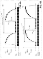


Classifications
-
- H—ELECTRICITY
- H05—ELECTRIC TECHNIQUES NOT OTHERWISE PROVIDED FOR
- H05B—ELECTRIC HEATING; ELECTRIC LIGHT SOURCES NOT OTHERWISE PROVIDED FOR; CIRCUIT ARRANGEMENTS FOR ELECTRIC LIGHT SOURCES, IN GENERAL
- H05B45/00—Circuit arrangements for operating light-emitting diodes [LED]
- H05B45/30—Driver circuits
- H05B45/37—Converter circuits
- H05B45/3725—Switched mode power supply [SMPS]
- H05B45/385—Switched mode power supply [SMPS] using flyback topology
-
- H—ELECTRICITY
- H02—GENERATION; CONVERSION OR DISTRIBUTION OF ELECTRIC POWER
- H02M—APPARATUS FOR CONVERSION BETWEEN AC AND AC, BETWEEN AC AND DC, OR BETWEEN DC AND DC, AND FOR USE WITH MAINS OR SIMILAR POWER SUPPLY SYSTEMS; CONVERSION OF DC OR AC INPUT POWER INTO SURGE OUTPUT POWER; CONTROL OR REGULATION THEREOF
- H02M3/00—Conversion of DC power input into DC power output
- H02M3/22—Conversion of DC power input into DC power output with intermediate conversion into AC
- H02M3/24—Conversion of DC power input into DC power output with intermediate conversion into AC by static converters
- H02M3/28—Conversion of DC power input into DC power output with intermediate conversion into AC by static converters using discharge tubes with control electrode or semiconductor devices with control electrode to produce the intermediate AC
- H02M3/325—Conversion of DC power input into DC power output with intermediate conversion into AC by static converters using discharge tubes with control electrode or semiconductor devices with control electrode to produce the intermediate AC using devices of a triode or a transistor type requiring continuous application of a control signal
- H02M3/335—Conversion of DC power input into DC power output with intermediate conversion into AC by static converters using discharge tubes with control electrode or semiconductor devices with control electrode to produce the intermediate AC using devices of a triode or a transistor type requiring continuous application of a control signal using semiconductor devices only
- H02M3/33507—Conversion of DC power input into DC power output with intermediate conversion into AC by static converters using discharge tubes with control electrode or semiconductor devices with control electrode to produce the intermediate AC using devices of a triode or a transistor type requiring continuous application of a control signal using semiconductor devices only with automatic control of the output voltage or current, e.g. flyback converters
-
- H—ELECTRICITY
- H02—GENERATION; CONVERSION OR DISTRIBUTION OF ELECTRIC POWER
- H02M—APPARATUS FOR CONVERSION BETWEEN AC AND AC, BETWEEN AC AND DC, OR BETWEEN DC AND DC, AND FOR USE WITH MAINS OR SIMILAR POWER SUPPLY SYSTEMS; CONVERSION OF DC OR AC INPUT POWER INTO SURGE OUTPUT POWER; CONTROL OR REGULATION THEREOF
- H02M3/00—Conversion of DC power input into DC power output
- H02M3/22—Conversion of DC power input into DC power output with intermediate conversion into AC
- H02M3/24—Conversion of DC power input into DC power output with intermediate conversion into AC by static converters
- H02M3/28—Conversion of DC power input into DC power output with intermediate conversion into AC by static converters using discharge tubes with control electrode or semiconductor devices with control electrode to produce the intermediate AC
- H02M3/325—Conversion of DC power input into DC power output with intermediate conversion into AC by static converters using discharge tubes with control electrode or semiconductor devices with control electrode to produce the intermediate AC using devices of a triode or a transistor type requiring continuous application of a control signal
- H02M3/335—Conversion of DC power input into DC power output with intermediate conversion into AC by static converters using discharge tubes with control electrode or semiconductor devices with control electrode to produce the intermediate AC using devices of a triode or a transistor type requiring continuous application of a control signal using semiconductor devices only
- H02M3/33507—Conversion of DC power input into DC power output with intermediate conversion into AC by static converters using discharge tubes with control electrode or semiconductor devices with control electrode to produce the intermediate AC using devices of a triode or a transistor type requiring continuous application of a control signal using semiconductor devices only with automatic control of the output voltage or current, e.g. flyback converters
- H02M3/33515—Conversion of DC power input into DC power output with intermediate conversion into AC by static converters using discharge tubes with control electrode or semiconductor devices with control electrode to produce the intermediate AC using devices of a triode or a transistor type requiring continuous application of a control signal using semiconductor devices only with automatic control of the output voltage or current, e.g. flyback converters with digital control
-
- H—ELECTRICITY
- H02—GENERATION; CONVERSION OR DISTRIBUTION OF ELECTRIC POWER
- H02M—APPARATUS FOR CONVERSION BETWEEN AC AND AC, BETWEEN AC AND DC, OR BETWEEN DC AND DC, AND FOR USE WITH MAINS OR SIMILAR POWER SUPPLY SYSTEMS; CONVERSION OF DC OR AC INPUT POWER INTO SURGE OUTPUT POWER; CONTROL OR REGULATION THEREOF
- H02M5/00—Conversion of AC power input into AC power output, e.g. for change of voltage, for change of frequency, for change of number of phases
- H02M5/02—Conversion of AC power input into AC power output, e.g. for change of voltage, for change of frequency, for change of number of phases without intermediate conversion into DC
- H02M5/04—Conversion of AC power input into AC power output, e.g. for change of voltage, for change of frequency, for change of number of phases without intermediate conversion into DC by static converters
- H02M5/22—Conversion of AC power input into AC power output, e.g. for change of voltage, for change of frequency, for change of number of phases without intermediate conversion into DC by static converters using discharge tubes with control electrode or semiconductor devices with control electrode
- H02M5/275—Conversion of AC power input into AC power output, e.g. for change of voltage, for change of frequency, for change of number of phases without intermediate conversion into DC by static converters using discharge tubes with control electrode or semiconductor devices with control electrode using devices of a triode or transistor type requiring continuous application of a control signal
- H02M5/293—Conversion of AC power input into AC power output, e.g. for change of voltage, for change of frequency, for change of number of phases without intermediate conversion into DC by static converters using discharge tubes with control electrode or semiconductor devices with control electrode using devices of a triode or transistor type requiring continuous application of a control signal using semiconductor devices only
-
- Y—GENERAL TAGGING OF NEW TECHNOLOGICAL DEVELOPMENTS; GENERAL TAGGING OF CROSS-SECTIONAL TECHNOLOGIES SPANNING OVER SEVERAL SECTIONS OF THE IPC; TECHNICAL SUBJECTS COVERED BY FORMER USPC CROSS-REFERENCE ART COLLECTIONS [XRACs] AND DIGESTS
- Y02—TECHNOLOGIES OR APPLICATIONS FOR MITIGATION OR ADAPTATION AGAINST CLIMATE CHANGE
- Y02B—CLIMATE CHANGE MITIGATION TECHNOLOGIES RELATED TO BUILDINGS, e.g. HOUSING, HOUSE APPLIANCES OR RELATED END-USER APPLICATIONS
- Y02B20/00—Energy efficient lighting technologies, e.g. halogen lamps or gas discharge lamps
- Y02B20/30—Semiconductor lamps, e.g. solid state lamps [SSL] light emitting diodes [LED] or organic LED [OLED]
Definitions
- the present invention relates generally to power converters, and more specifically to power converters utilized with dimmer circuits.
- Switched mode power converters are commonly used due to their high efficiency, small size and low weight to power many of today's electronics.
- Conventional wall sockets provide a high voltage alternating current.
- a switching power converter a high voltage alternating current (ac) input is converted to provide a well regulated direct current (dc) output through an energy transfer element.
- the switched mode power converter control circuit usually provides output regulation by sensing one or more inputs representative of one or more output quantities and controlling the output in a closed loop.
- a switch is utilized to provide the desired output by varying the duty cycle (typically the ratio of the on time of the switch to the total switching period), varying the switching frequency or varying the number of pulses per unit time of the switch in a switched mode power converter.
- a triac dimmer circuit typically disconnects a portion of the ac input voltage to limit the amount of voltage and current supplied to an incandescent lamp. This is known as phase dimming because it is often convenient to designate the position of the triac dimmer circuit and the resultant amount of missing voltage in terms of a fraction of the period of the ac input voltage measured in degrees.
- the ac input voltage is a sinusoidal waveform and the period of the ac input voltage is referred to as a full line cycle.
- half the period of the ac input voltage is referred to as a half line cycle.
- An entire period has 360 degrees, and a half line cycle has 180 degrees.
- the phase angle is a measure of how many degrees (from a reference of zero degrees) of each half line cycle the triac dimmer circuit disconnects the ac input.
- removal of half the ac input voltage in a half line cycle by the triac dimmer circuit corresponds to a phase angle of 90 degrees.
- removal of a quarter of the ac input voltage in a half line cycle may correspond to a phase angle of 45 degrees.
- the conduction angle is a measure of how many degrees (from a reference of zero degrees) of each half line cycle the triac dimmer circuit does not disconnect a portion of the ac input voltage from the power converter.
- the conduction angle is a measure of how many degrees of each half line cycle in which the triac dimmer circuit is conducting.
- the removal of a quarter of the ac input voltage in a half line cycle may correspond to a phase angle of 45 degrees but a conduction angle of 135 degrees.
- LED lamps often require a regulated power converter to provide regulated current and voltage from the ac power line.
- Most LEDs and Led modules are best driven by a regulated current which a regulated power converter may provide from an ac power line.
- Triac dimmer circuits typically don't work well with conventional regulated power converter controllers.
- Regulated power converters are typically designed to ignore distortions of the ac input voltage. Their purpose is to deliver a constant regulated output until a low input RMS voltage causes them to shut off completely. As such, conventional regulated power supplies would not dim the LED lamp.
- a power converter may include an improved conventional power converter controller that is designed to respond to a triac dimmer circuit by directly sensing the average value of the dimmer circuit output (in other words, the average value of the ac input voltage after the triac dimmer circuit has removed a portion of the ac input voltage) to determine the amount of dimming requested.
- the improved conventional power converter controller utilizes this relationship to indirectly determine the phase angle and alter the quantity to which the output of the power converter is regulated.
- the amount of dimming detected is subject to variances of the ac input voltage.
- the accuracy of the phase angle measured through the average value of the dimmer circuit output is dependent on variances of the ac input voltage.
- phase dimmer circuit typically disconnects the ac input voltage for a portion of every half line cycle to limit the amount of voltage and current supplied to the LEDs.
- the phase angle is a measure of how many degrees of each half line cycle the dimmer circuit has disconnected the input.
- the amount of the ac input voltage which the dimmer circuit does not disconnect may be referred to as the conduction angle.
- the amount of dimming set by the dimmer circuit may be determined by measuring the amount of time which the ac input voltage is disconnected (i.e., the amount of time which the dimmer circuit is not conducting) or the amount of time which the ac input voltage is not disconnected (i.e. the amount of time which the dimmer circuit is conducting).
- the amount of dimming set by the dimmer circuit may be directly measured from input voltage of the power converter.
- One way which the conduction angle (or phase angle) may be measured by threshold detection where the input voltage may be compared to a reference threshold.
- the amount of time which the input voltage is above the reference may correspond to the conduction angle of the dimmer circuit.
- the amount of time which the input voltage is below the reference may correspond to the phase angle.
- measuring the conduction angle (or phase angle) utilizing threshold detection may be inaccurate due to leakage energy and capacitors in the power supply which prevent the input voltage falling to substantially zero.
- an "edge” may be observed in the waveform of input voltage of the power supply.
- the input voltage is substantially zero until the dimmer circuit conducts. Once the dimmer circuit begins to conduct, the input voltage rapidly increases and follows the ac input voltage.
- the input voltage substantially follows the ac input voltage until the dimmer circuit does not conduct and the input voltage rapidly decreases to substantially zero. The rapid increase or decrease may be referred to as an edge.
- an edge detection circuit may be utilized to determine if the dimmer circuit is or is not conducting. Once an edge is detected, the conduction angle (or phase angle) may be measured.
- the edge detection circuit may generate a count signal which tracks the input of the power converter. If the count signal is unable the track the input of the power converter for a given amount of time, an edge in the input is detected.
- the count signal is a rectangular pulse waveform with varying lengths of logic high and logic low sections. When the count signal is tracking the input, the count signal increases and decreases within the given amount of time. However, if the count signal is no longer tracking the input, the count signal may substantially increase within the given amount of time or substantially decrease within the given amount of time.
- FIG. 1 a functional block diagram of an example power converter 100 is illustrated including ac input voltage V AC 102, a dimmer circuit 104, a dimmer output voltage V DO 106, a rectifier 108, a rectified voltage V RECT 110, an energy transfer element T1 112, a primary winding 114 of the energy transfer element T1 112, a secondary winding 116 of the energy transfer element T1 112, a switch S1 118, input return 117, a clamp circuit 120, a rectifier D1 122, an input capacitor C F 121, an output capacitor C1 124, a load 126, a sense circuit 128, and a controller 130.
- Controller 130 further includes a drive circuit block 132, an oscillator 134, and an edge detection circuit 136.
- Edge detection circuit 136 is shown as including a comparator 138, a count module 140, and an edge checking module that includes a leading edge check block 142 and/or a trailing edge check block 144.
- sense circuit 128 may also be included in controller 130.
- FIG. 1
- the example switched mode power converter 100 illustrated in FIG. 1 is coupled in a flyback configuration, which is just one example of a switched mode power converter that may benefit from the teachings of the present invention. It is appreciated that other known topologies and configurations of switched mode power converter may also benefit from the teachings of the present invention.
- the example power converter in FIG. 1 is an isolated power converter. It should be appreciated that non-isolated power converters may also benefit from the teachings of the present invention.
- the power converter 100 provides output power to the load 126 from an unregulated input voltage.
- the input voltage is the ac input voltage V AC 102.
- the input voltage is a rectified ac input voltage such as rectified voltage V RECT 110.
- dimmer circuit 104 receives the ac input voltage V AC 102 and produces the dimmer output voltage V DO 106.
- the dimmer circuit 104 may be utilized to limit the voltage delivered to the power converter 100.
- the dimmer circuit 104 may be a phase dimming circuit such as a triac phase dimmer.
- the dimmer circuit 104 further couples to the rectifier 108 and the dimmer output voltage V DO 106 is received by the rectifier 108.
- the rectifier 108 outputs rectified voltage V RECT 110.
- rectifier 108 may be a bridge rectifier.
- the rectifier 108 further couples to the energy transfer element T1 112.
- the energy transfer element T1 112 may be a coupled inductor.
- the energy transfer element 110 may be an inductor.
- the energy transfer element T1 112 may be a transformer.
- the energy transfer element T1 112 includes two windings, a primary winding 114 and a secondary winding 116.
- the energy transfer element T1 112 may have more than two windings.
- primary winding 114 may be considered an input winding
- secondary winding 116 may be considered an output winding.
- the primary winding 114 is further coupled to switch S1 118, which is then further coupled to input return 117.
- the clamp circuit 120 is illustrated in the example of FIG. 1 as being coupled across the primary winding 114 of the energy transfer element T1 112.
- the filter capacitor C F 121 may couple across the primary winding 114 and switch S1 118.
- the filter capacitor C F 121 may couple to the rectifier 108 and input return 117.
- Secondary winding 116 of the energy transfer element T1 112 is coupled to the rectifier D1 122.
- the rectifier D1 122 is exemplified as a diode.
- the rectifier D1 122 may be a transistor used as a synchronous rectifier. Both the output capacitor C1 124 and the load 126 are shown in FIG.
- load 126 may be a light emitting diode (LED), an LED module, or an LED array.
- LED light emitting diode
- the power converter 100 further comprises circuitry to regulate the output which is exemplified as output quantity Uo 150.
- the output quantity Uo 150 is either an output voltage V O 146, an output current I O 148, or a combination of the two.
- a sense circuit 128 is coupled to sense the output quantity Uo 150 and to provide feedback signal U FB 152, which is representative of the output quantity Uo 150.
- Feedback signal U FB 152 may be a voltage signal or a current signal.
- the sense circuit 128 may sense the output quantity Uo 150 from an additional winding included in the energy transfer element T1 112. In another example, there may be a galvanic isolation (not shown) between the controller 130 and the sense circuit 128.
- the galvanic isolation could be implemented by using devices such as an opto-coupler, a capacitor or a magnetic coupling.
- the sense circuit 128 may utilize a voltage divider to sense the output quantity Uo 150 from the output of the power converter 100.
- Controller 130 is coupled to the sense circuit 128 and receives the feedback signal U FB 152 from the sense circuit 128.
- the controller 130 further includes terminals for receiving the voltage sense signal 154, current sense signal 158 and for providing the drive signal 170 to power switch S1 118.
- the voltage sense signal 154 may be representative of the rectified voltage V RECT 110.
- the voltage sense signal 154 may be representative of the dimmer output voltage V DO 106.
- the voltage sense signal 158 may be a voltage signal or a current signal.
- the current sense signal 158 may be representative of the switch current I D 156 in the power switch S1 118.
- Current sense signal 158 may be a voltage signal or a current signal.
- controller 130 provides drive signal 170 to the power switch S1 118 to control various switching parameters to control the transfer of energy from the input of power converter 100 to the output of power converter 100.
- switching parameters may include switching frequency, switching period, duty cycle, or respective ON and OFF times of the power switch S1 118.
- controller 130 includes the drive circuit 132, oscillator 134, and the edge detection circuit 136.
- the drive circuit is coupled to output the drive signal 170 to control switching of the power switch S1 116 in response to the one or more outputs of the edge detection circuit 136 and/or the feedback signal U FB 152.
- the drive circuit may also be coupled to be responsive to the current sense signal 158.
- a single controller is illustrated in FIG. 1 , it should be appreciated that multiple controllers may be utilized by the power converter 100.
- the drive circuit 132, oscillator 134, and edge detection circuit 136 need not be within a single controller.
- the power converter 100 may have a primary controller coupled to the input side of the power converter 100 and a secondary controller coupled to the output side of the power converter 100.
- the edge detection circuit 136 includes the comparator 138, count module 140, leading edge check block 142 and the trailing edge check block 144.
- the edge detection circuit 136 may include either the leading edge check block 142 or the trailing edge check block 144, or both in its edge checking module (not illustrated).
- Edge detection circuit 136 is coupled to receive the voltage sense signal 154 and the system clock 160 and output the leading edge signal U LE 167 or the trailing edge signal U TE 168, or both signals.
- the leading edge signal U LE 167 and the trailing edge signal U TE 168 confirm whether a leading edge dimmer circuit or a trailing edge dimmer circuit is detected (respectively).
- count module 140, leading edge check block 142, and trailing edge check block 144 may all be coupled to receive the system clock 160.
- Comparator 138 is coupled to output compare signal 164 in response to comparing input sense signal 154 and count signal 162. As illustrated, comparator 138 receives the voltage sense signal 154 and count signal U COUNT 162 from the count module 140 and outputs the result of the comparison to the count module 140, leading edge check block 142, and the trailing edge check block 144. Count module 140 is coupled to adjust count signal 162 to track input sense signal 154 in response to receiving compare signal 164. In particular, count module 140 varies the count signal U COUNT 162 in response to the comparison of the voltage sense signal 154 with the count signal U COUNT 162, as will be discussed further.
- the count module 140 increases the count signal U COUNT 162 if the input voltage provided by the voltage sense signal 154 is greater than the count signal U COUNT 162 and decreases the count signal U COUNT 162 if the input voltage provided by the voltage sense signal 154 is less than the count signal U COUNT 162.
- Leading edge check block 142 and trailing edge check block 144 each receive the output of the comparator 138 and determines whether a leading edge or a trailing edge is detected and outputs the leading edge signal U LE 167 and the trailing edge signal U TE 168, respectively to the drive circuit 132.
- the leading edge check block 142 and trailing edge check block 144 output a leading edge or trailing edge signal in response to compare signal 164 not changing between a first state and a second state for a given time period.
- the leading edge check block 142 outputs a leading edge signal if the count signal U COUNT 162 is less than the voltage sense signal 154 for a given amount of time.
- the trailing edge check block 144 outputs the trailing edge signal if the count signal U COUNT 162 is greater than the voltage sense signal 154 for a given amount of time.
- the power converter 100 of FIG. 1 provides output power to the load 126 from an unregulated input such as the ac input voltage V AC 102.
- the dimmer circuit 104 may be utilized to limit the amount of voltage delivered to the power converter. For the example of a LED load, when the dimmer circuit 104 limits the amount of voltage delivered to the power converter, the resultant current delivered to the load of LED arrays by the controller 130 is also limited and the LED array dims.
- the dimmer circuit 104 may be a phase dimming circuit such as a triac dimmer circuit or a Metal-Oxide-Semiconductor Field Effect Transistor ("MOSFET”) dimmer circuit.
- MOSFET Metal-Oxide-Semiconductor Field Effect Transistor
- the dimmer circuit 104 disconnects the ac input voltage V AC 102 when the ac input voltage V AC 102 crosses zero voltage. After a given amount of time, the dimmer circuit 104 reconnects the ac input voltage V AC 102 with the power converter 100. The amount of time before the dimmer circuit reconnects the ac input voltage V AC 102 is set by a user. For trailing edge dimming, the dimmer circuit 104 connects the input to the power converter when the ac input voltage V AC 102 crosses zero voltage. After a given amount of time set by a user, the dimmer circuit 104 then disconnects the ac input voltage V AC 102 for the remainder of the half cycle.
- the dimmer circuit 104 may interrupt the phase of the ac input voltage V AC 102.
- the dimmer circuit 104 controls the amount of time the ac input voltage V AC 102 is disconnected from the power converter. In general, the more dimming wanted corresponds to a longer period of time during which the dimming circuit 104 disconnects the ac input voltage V AC 102.
- the dimmer circuit 104 produces the dimmer output voltage V DO 106 which is received by rectifier 108.
- the rectifier 108 produces the rectified voltage V RECT 110.
- the filter capacitor C F 121 filters the high frequency current from the switch S1 118.
- the filter capacitor C F 121 may be large enough such that a substantially dc voltage is applied to the energy transfer element T1 112.
- PFC power factor correction
- a small filter capacitor C F 121 may be utilized to allow the voltage applied to the energy transfer element T1 112 to substantially follow the rectified voltage V RECT 110.
- the value of the filter capacitor C F 121 may be chosen such that the voltage on the filter capacitor C F 121 reaches substantially zero during each half-line cycle of the ac input voltage V AC 102. Or in other words, the voltage on the filter capacitor C F 121 substantially follows the positive magnitude of the dimmer output voltage V DO 106.
- the controller 130 may detect when the dimmer circuit 104 disconnects and reconnects the ac input voltage VAC 102 from the power converter 100 by sensing the voltage on the filter capacitor C F 121 (or in other words the rectified voltage V RECT 110).
- the controller 130 may detect when the dimmer circuit 104 disconnects and reconnects the ac input voltage V AC 102 from the power converter 100 by sensing the switch current I D 156. In a further example, the controller 130 may detect that the dimmer circuit 103 disconnects and reconnects the ac input voltage V AC 102 from the power converter 100 by sensing the input current (in one example, the current flowing between the rectifier 108 and the capacitor C F 121).
- the switching power converter 100 utilizes the energy transfer element T1 112 to transfer voltage between the primary 114 and the secondary 116 windings.
- the clamp circuit 120 is coupled to the primary winding 114 to limit the maximum voltage on the switch S1 118.
- Switch S1 118 is opened and closed in response to the drive signal 170. It is generally understood that a switch that is closed may conduct current and is considered on, while a switch that is open cannot conduct current and is considered off.
- the switch S1 118 may be a transistor such as a metal-oxide-semiconductor field-effect transistor (MOSFET).
- controller 130 may be implemented as a monolithic integrated circuit or may be implemented with discrete electrical components or a combination of discrete and integrated components.
- Controller 130 and switch S1 118 could form part of an integrated circuit that is manufactured as either a hybrid or monolithic integrated circuit.
- the switching of the switch S1 118 produces a pulsating current at the rectifier D1 122.
- the current in the rectifier D1 122 is filtered by the output capacitor C1 124 to produce a substantially constant output voltage Vo 146, output current I O 148, or a combination of the two at the load 126.
- the sense circuit 128 senses the output quantity Uo 150 of the power converter 100 to provide the feedback signal U FB 152 to the controller 130.
- the feedback signal U FB 152 may be a voltage signal or a current signal and provides information regarding the output quantity Uo 152 to the controller 130.
- the controller 130 receives the current sense input signal 158 which relays the switch current I D 156 in the switch S1 118.
- the switch current I D 156 may be sensed in a variety of ways, such as for example the voltage across a discrete resistor or the voltage across a transistor when the transistor is conducting.
- the controller 130 may receive the voltage sense input signal 154 which relays the value of the rectified voltage V RECT 110.
- the rectified voltage V RECT 110 may be sensed a variety of ways, such as for example through a resistor divider.
- Edge detection circuit 136 is coupled to output the leading edge signal U LE 167 or the trailing edge signal U TE 168 in response to the voltage sense signal 154 if a leading edge or a trailing edge is detected.
- Leading edge signal U LE 167 or the trailing edge signal U TE 168 may be analog or digital signals with a logic high value corresponding to an edge being detected and a logic low value corresponding to no edge detected.
- the comparator 138 compares the rectified voltage V RECT 110 (via voltage sense 154) with the count signal U COUNT 162. If the rectified voltage V RECT 110 is greater than the count signal U COUNT 162, count module 140 increments the value of the count signal U COUNT 162.
- count module 140 decrements the value of the count signal U COUNT 162. As such, when the dimmer circuit 104 is not disconnecting the ac input voltage V AC 102 from the power converter, the count signal U COUNT 162 substantially tracks the rectified voltage V RECT 110. In other words, the value of the count signal U COUNT 162 increases and decreases within a given amount of time to track rectified voltage V RECT 110.
- the count signal U COUNT 162 loses track of the rectified voltage V RECT 110 and either consistently increases or decreases depending if the dimmer circuit 104 is a leading or trailing edge dimmer. In one example, the count signal U COUNT 162 is unable to track the edges of the rectified voltage V RECT 110 due to the frequency of the system clock 160 in comparison to the frequency of the edge.
- the rectified voltage V RECT 110 sharply increases once the dimmer circuit 104 fires. As such, the rectified voltage V RECT 110 is greater than the count signal U COUNT 162 for a given amount of time.
- the leading edge check block 142 receives compare signal 164 from comparator 138 and asserts the leading edge signal U LE 167 if the rectified voltage V RECT 110 is greater than the count signal U COUNT 162 for a given amount of time.
- the rectified voltage V RECT 110 sharply decreases once the dimmer circuit is disconnected. As such the rectified voltage V RECT 110 is less than the count signal U COUNT 162 for a given amount of time.
- the trailing edge check block 144 receives compare signal 164 and asserts the trailing edge signal U TE 168 if the rectified voltage V RECT 110 is less than the count signal U COUNT 162 for a given amount of time.
- FIG. 2 illustrates example waveforms of an ac input voltage 202, a dimmer output voltage V DO 206, and a rectified voltage V RECT 210.
- FIG. 2 illustrates the dimmer output voltage V DO 206 and a resultant rectified voltage V RECT 210 for leading edge triac dimming.
- the ac input voltage V AC 202 is a sinusoidal waveform with the period of the ac input voltage V AC 202 referred to as a full line cycle T FL 211.
- V AC V P sin(2 ⁇ f L t ).
- V P 207 is the peak voltage of the ac input voltage V AC
- f L is the frequency of the ac input voltage.
- a full line cycle T HL 211 of the ac input voltage 202 is denoted as the length of time between every other zero-crossing of the ac input voltage 202.
- the half line cycle T HL 213 of the ac input voltage V AC 202 is denoted as the length of time between consecutive zero-crossings.
- the dimmer circuit 104 disconnects the ac input voltage V AC 202 from the power converter when the ac input voltage V AC 202 substantially crosses zero voltage. After a given amount of time, the dimmer circuit 104 reconnects the ac input voltage V AC 202 with the power converter 100 and the dimmer output voltage V DO 206 substantially follows the ac input voltage V AC 202. In other words, the dimmer circuit 104 disconnects the ac input voltage 202 for a portion of the half line cycle to provide the dimmer output voltage V DO 206 thus limiting the amount of voltage and current supplied to a load (such as an LED lamp).
- a load such as an LED lamp
- the rectifier circuit 104 rectifies the dimmer output voltage V DO 206 thus providing the rectified voltage V RECT 210 as shown.
- the beginning of each half line cycle T HL 202 of the rectified voltage V RECT 210 is substantially equal to zero voltage corresponding to when the dimmer circuit 104 disconnects the ac input voltage V AC 202 from the power converter.
- the dimmer output voltage V DO 206 sharply increases (or decreases) to substantially follow the ac input voltage V AC 202.
- the sharp increase is also illustrated in the example waveform of the rectified voltage V RECT 210.
- the sharp increase may be referred to as the "edge.”
- example waveforms of the rectified voltage V RECT 310, system clock 360, and the count signal U COUNT 362 of the switching power converter 100 are illustrated including half line cycle T HL 313, system period T SYS 374, and times t 1 -t 5 .
- FIG. 3B illustrates the rectified voltage V RECT 310, system clock 360, and the count signal U COUNT 362 for the portion 372 of FIG. 3A . It should be appreciated that only one half line cycle T HL 313 is illustrated for clarity.
- FIG. 3A illustrates one half line cycle T HL 313 of the rectified voltage V RECT 310, system clock 360, and the count signal U COUNT 362 when the dimmer circuit is not disconnecting a portion of the ac input voltage V AC 102 from the power converter 100.
- the rectified voltage V RECT 310 has a substantially sinusoidal shape with no edges.
- the system clock 360 is shown as a rectangular pulse waveform with logic high and logic low sections.
- the period of the system clock T SYS 374 is shorter than the one half line cycle T HL 313.
- the frequency of the system clock 360 is faster than the line frequency of the ac input voltage V AC 102.
- FIG. 3A illustrates the system clock 360 as notches to demonstrate that the system period T SYS 374 is shorter than the full and half line cycle.
- the full line cycle T FL 311 is 4096 times greater than the system period T SYS 374 of the system clock 360.
- Count signal U COUNT 362 is a rectangular pulse waveform which may have multiple values, in the illustrated embodiment.
- U COUNT 362 may be a digital number broadcasted as a digital word.
- the count signal U COUNT 362 may be an analog representation of a digital number.
- the value (or magnitude) of the count signal U COUNT 362 may correspond to a digital number.
- the count signal U COUNT 362 substantially follows the rectified voltage V RECT 310 or at least a scaled-down version of V RECT 310 (e.g. input sense signal 154).
- the count signal U COUNT 362 increases and decreases such that the count signal U COUNT 362 crosses the rectified voltage V RECT 310 within a given amount of time.
- the given amount of time may be N number of consecutive system periods T SYS 374.
- the count signal U COUNT 362 substantially tracks the rectified voltage V RECT 310 if the count signal U COUNT 362 crosses the rectified voltage V RECT 310 within N number of consecutive system periods T SYS 374.
- N may be substantially equal to 10.
- FIG. 3B illustrates the portion 372 of FIG. 3A .
- the count signal U COUNT 362 may cross the rectified voltage V RECT 310 several times.
- times t 1 -t 5 correspond to the rising edges of the system clock 360 and the time between rising edges is substantially the system period T SYS 374.
- the value of count signal U COUNT 362 is less than rectified voltage V RECT 310.
- Comparator 138 gives compare signal 164 a second state (e.g. logic high) when U COUNT 362 is less than V RECT 310.
- the count module 140 increments the count signal U COUNT 362 in response to compare signal 164 having the second state and the value of the count signal U COUNT 362 increases and crosses rectified voltage V RECT 310.
- the value of the count signal U COUNT 362 is greater than the rectified voltage V RECT 310.
- comparator 138 gives compare signal 164 a first state (e.g. logic low) when U COUNT 362 is greater than V RECT 310.
- Count module 140 decrements the count signal U COUNT 362 in response to compare signal 164 having the first state and the value of the count signal U COUNT 362 decreases and crosses the rectified voltage V RECT 310.
- the amounts which the count signal U COUNT 362 increases and decreases may be fixed and the resultant value after each increase and decrease may correspond to a digital count.
- the value of the count signal U COUNT 362 is less than the rectified voltage V RECT 310. As such, the value of the count signal U COUNT 362 is increased in response to compare signal 164 having the second state. However, the value of the count signal U COUNT 362 at next system clock period (shown as time t 4 ) is still less than the rectified voltage V RECT 310.
- Count module 140 further increments the count signal U COUNT 362 and the value of the count signal U COUNT 362 increases to the next value. At time t4, the count signal U COUNT 362 crosses rectified voltage V RECT 310.
- the value of the count signal U COUNT 362 is greater than the rectified voltage V RECT 310 and the value of the count signal U COUNT 362 decreases. As shown at time t 5 , the count signal U COUNT 362 crosses rectified voltage V RECT 310. In the example shown in FIG. 3B , the count signal U COUNT 362 does not cross the rectified voltage V RECT 310 for two consecutive switching periods T SYS 374 of the system clock. As mentioned above, the count signal U COUNT 362 substantially tracks the rectified voltage V RECT 310 if the count signal U COUNT 362 crosses the rectified voltage V RECT 310 within N number of consecutive system periods T SYS 374.
- the count signal U COUNT 362 illustrated in FIG. 3B is still tracking the rectified voltage V RECT 310 or at least a scaled version of V RECT 310 (e.g. input sense signal 154) since the number of consecutive switching periods which the count signal U COUNT 362 does not cross the rectified voltage V RECT 310 (i.e. 2) is less than 10.
- FIG. 4A example waveforms of the rectified voltage V RECT 410, system clock 460, and the count signal U COUNT 462 of the switching power converter 100 are illustrated including half line cycle T HL 413 and the system period T SYS 474.
- FIG.4A illustrates the example rectified voltage V RECT 410 for a leading edge dimmer circuit.
- each half line cycle T HL 413 of the rectified voltage V RECT 410 is substantially equal to zero voltage corresponding to when the dimmer circuit 104 disconnects the ac input voltage V AC 102 from the power converter 100.
- the rectified voltage V RECT 410 substantially follows the positive magnitude of the ac input voltage V AC 102.
- the count signal U COUNT 462 is a rectangular pulse waveform with multiple values. As shown, the count signal U COUNT 462 may partially track the rectified voltage V RECT 410.
- the count signal U COUNT 462 is unable to track the rectified voltage V RECT 410.
- the count signal U COUNT 462 is less than the rectified voltage V RECT 410 for multiple periods of the system clock 460.
- the count signal U COUNT 462 is less than the rectified voltage V RECT 410 for fourteen consecutive periods of the system clock 460.
- the count module 140 increments the count signal U COUNT 462 for fourteen consecutive periods and the value of the count signal U COUNT 462 increases for fourteen consecutive periods of the system clock 460.
- the count signal U COUNT 462 does not cross the rectified voltage V RECT 410 within N consecutive periods of the system clock 460 and an edge is detected.
- the count signal U COUNT 462 increasing for N or more consecutive system periods would correspond to a detected leading edge.
- the number of consecutive periods of the clock signal which the count signal U COUNT 462 is less than the rectified voltage V RECT 410 may be referred to as the leading edge count.
- example waveforms of the rectified voltage V RECT 410, system clock 460, and the count signal U COUNT 462 of the switching power converter 100 are illustrated including half line cycle T HL 413 and the system period T SYS 474.
- FIG.4B illustrates the example rectified voltage V RECT 410 for a trailing edge dimmer circuit.
- FIG. 4B is similar to FIG. 4A , however the dimmer circuit 104 connects the input to the power converter 100 to the ac input voltage V AC 102 when the ac input voltage V AC 102 crosses zero voltage and after a given amount of time, the dimmer circuit 104 then disconnects the ac input voltage V AC 102 for the remainder of the half line cycle T HL 413.
- the rectified voltage V RECT 410 substantially follows the positive magnitude of the ac input voltage V AC 102 until the dimmer circuit 104 disconnects the ac input voltage V AC 102 from the power converter 100.
- the value of the rectified voltage V RECT 410 then falls to substantially zero voltage until the beginning of the next half line cycle.
- the decrease of the rectified voltage V RECT 410 may be referred to as the trailing edge.
- the count signal U COUNT 462 may partially track the rectified voltage V RECT 410. However, at the trailing edge of the rectified voltage V RECT 410, the count signal U COUNT 462 is unable to track the rectified voltage V RECT 410.
- the count signal U COUNT 462 is greater than the rectified voltage V RECT 410 for multiple periods of the system clock 460. In the illustrated example, the count signal U COUNT 462 is greater than the rectified voltage V RECT 410 for fifteen consecutive periods of the system clock 460.
- the count module 140 decrements the count signal U COUNT 462 for fifteen consecutive periods and the value of the count signal U COUNT 462 decreases for fourteen consecutive periods of the system clock 460.
- the count signal U COUNT 462 does not cross the rectified voltage V RECT 410 within N consecutive periods of the system clock 460 and an edge is detected.
- the count signal U COUNT 462 decreasing for N or more consecutive system periods would correspond to a detected trailing edge.
- the number of consecutive periods of the clock signal which the count signal U COUNT 462 is greater than the rectified voltage V RECT 410 may be referred to as the trailing edge count.
- FIG. 5 is a flow diagram illustrating an example process 500 for detecting an edge in an input waveform in accordance with an example of the present invention.
- the order in which some or all of the process blocks appear in process 500 should not be deemed limiting. Rather, one of ordinary skill in the art having the benefit of the present disclosure will understand that some of the process blocks may be executed in a variety of orders not illustrated, or even in parallel.
- process block 505 the voltage sense signal (e.g. voltage sense signal 154) is compared with the count signal U COUNT (e.g. count signal U COUNT 162).
- process block 510 process 500 determines whether the count signal U COUNT is greater than the voltage sense signal. If the count signal U COUNT is greater than the voltage sense signal, the process moves to block 515 and the count signal U COUNT is decremented or decreased. However, if the count signal U COUNT is not greater than the voltage sense signal, the process moves to block 520 and the count signal is U COUNT incremented or increased.
- the process determines if the leading edge count is greater than the first threshold (e.g. ten). If the leading edge count is not greater than the first threshold, the process returns to block 505. If the leading edge count is greater than the first threshold, the process asserts the leading edge confirmed signal (e.g. leading edge signal U LE 167) in block 545.
- the first threshold e.g. ten
- the process determines if the trailing edge count is greater than the second threshold (e.g. 10). If the trailing edge count is not greater than the second threshold, the process returns to block 505. If the trailing edge count is greater than the second threshold, the process asserts the trailing edge confirmed signal (e.g. trailing edge signal U TE 168) in block 550.
- the first threshold and the second threshold may correspond to the N number of consecutive periods of the system clock which the count signal is unable to track the rectified voltage. In addition, the first threshold and the second threshold may be the same threshold.
- FIG. 6 illustrates an example edge detection circuit 636 including a count module 640, leading edge check circuit 642, trailing edge check circuit 644, a resistor 674, a current mirror including transistors 676 and 677, and a driver 678.
- Count module 640 is shown including a counter 679 and an M bit DAC 681.
- Leading edge check circuit 642 includes counter 682 and digital comparator 683.
- trailing edge check circuit 644 includes counter 684 and digital comparator 685.
- FIG. 6 also includes input voltage sense signal 654, input voltage sense current I VIN 675, count signal I COUNT 662, system clock 660, comparator output 664 (i.e. compare signal 664), leading edge signal U LE 667 and trailing edge signal U TE 668, first threshold TH1 691, and second threshold TH2 692.
- input voltage sense signal 654 may be a voltage signal.
- the resistor 674 is coupled to receive the input voltage sense signal 654 and convert the voltage signal to a current signal, shown as input voltage sense current I VIN 675.
- Transistors 676 and 677 are coupled together as a current mirror. In the example illustrated, the ratio of the current mirror is 1:1 however, other ratios may be used.
- the first transistor 676 is coupled to receive the input voltage sense current I VIN 675 and the input voltage sense current I VIN 675 is mirrored to the second transistor 677.
- the count signal U COUNT is exemplified as a current signal, count signal I COUNT 662.
- the comparator 138 is exemplified by the terminal 638 since both the count signal I COUNT 662 and the input voltage sense current I VIN 675 are current signals.
- One end of driver 678 is coupled to the terminal 638 and the output 664 (compare signal 664) of the driver 678 is received at counters 679, 682, and 684.
- the compare signal 664 is received at the UP/DOWN input of counter 679 and is received at the COUNT/RESET inputs of counters 682 and 684.
- each of counters 679, 682, and 684 also receive system clock 660 at their clock inputs.
- the output of counter 679 is a digital word of M length and is referred to as digital count U DC 680.
- the digital count U DC 680 is coupled to be received by the M bit DAC 681 which converters the digital count U DC 680 to an analog signal.
- the digital count U DC 680 is converted to the count signal I COUNT 662 where magnitudes of the count signal I COUNT 662 correspond to a specific count of the digital count U DC 680.
- the outputs of counters 682 and 684 are coupled to be received by digital comparators 683 and 685, respectively.
- the digital comparators 683 and 685 are also coupled to receive the first threshold TH1 691 and the second threshold TH2 692, respectively.
- digital comparator 683 is coupled to compare the output of counter 682 with the first threshold TH1 691.
- the output of digital comparator 683 is the leading edge signal U LE 667. A logic high value of the leading edge signal U LE 667 may correspond to the output of counter 682 being greater than the first threshold TH1 691while a logic low value may correspond to the output of counter 682 being less than the first threshold TH1 691.
- the digital comparator 685 compares the output of the counter 684 with the second threshold TH2 692.
- the output of the digital comparator 685 is the trailing edge signal U TE 668.
- a logic high value of the trailing edge signal U TE 668 may correspond to the output of counter 684 being greater than the second threshold TH2 692while a logic low value may correspond to the output of counter 684 being less than the second threshold TH2 692.
- the input voltage sense current I VIN 675 is compared to the count signal I COUNT 662 at terminal 638. In one example, if the input voltage sense current I VIN 675 is greater than the count signal I COUNT 662, the voltage at terminal 638 is pulled high. The output 664 (count signal 664) of the driver 678 is a logic high value and the value stored in counter 679 is incremented. If the count signal I COUNT 662 is greater than the input voltage sense current I VIN 675, the voltage at terminal 638 is pulled low and the output 664 (compare signal 664) of the driver is a logic low value and the value stored in counter 679 is decremented.
- counter 679 When counter 679 receives a logic high value, the value of the digital count U DC 680 is incremented. When the counter 679 receives a logic low value, the value of the digital count U DC 680 is decremented.
- the M bit DAC 681 converts the digital count U DC 680 to an analog count signal I COUNT 662.
- counter 682 of the leading edge check circuit 642 increments when the output 664 is logic high and resets when the output 664 is logic low. As such, the value of the counter 682 increases with every consecutive period of the system clock which the input voltage sense current I VIN 675 is greater than the count signal I COUNT 662.
- the output of the counter 682 is compared to a first threshold TH1 691.
- the digital comparator 683 outputs a logic high value when the output of counter 682 is greater than the first threshold TH1 691 and a logic low value otherwise.
- the counter 684 of the trailing edge check circuit 644 increments when the output 664 is logic low and resets when the output 664 is logic high.
- the value of the counter 682 increases with every consecutive period of the system clock which the count signal I COUNT 662 is greater than the input voltage sense current I VIN 675.
- the output of the counter 684 is compared to a second threshold TH2 692.
- the digital comparator 685 outputs a logic high value when the output of counter 684 is greater than the second threshold TH2 692 and a logic low value otherwise.
- FIG. 7 illustrates an example leading edge check circuit 742 and trailing edge check circuit 744 including a shift register 786, decoder 788, digital comparator 790, and digital comparator 789.
- FIG. 7 also includes system clock 760, compare signal 764, the leading edge signal U LE 767, the trailing edge signal U TE 768, an upper threshold THU 793, and a lower threshold THL 794.
- Shift register 786 is coupled to receive the compare signal 764 and the system clock 760 and also coupled to the decoder 788. As mentioned above, the compare signal 764 may be logic high or logic low depending on whether the input signal is greater than the count signal. Shift register 786 may include L number of registers (illustrated as P1, P2, P3, P4, PL) which may store L number of values of the compare signal 764. In one example, each register (P1, P2, P3, P4, PL) of the shift register 786 may be a one bit register. The values stored in each individual register of the shift register 786 may be received by the decoder 788. In one example, the decoder 788 may determine the number of (logic) ones stored in the shift register 786.
- the decoder may determine the number of (logic) zeros stored in the shift register 786.
- Digital comparators 789 and 790 are coupled to the decoder to receive the output of the decoder 788.
- the output of the digital comparator 790 is the leading edge signal U LE 767 while the output of digital comparator 789 is the trailing edge signal U TE 768.
- the leading edge signal U LE 767 and the trailing edge signal U TE 768 may be rectangular pulse waveforms with varying lengths of logic high and logic low sections.
- the leading edge signal U LE 767 may be logic high when a leading edge is detected or may pulse to a logic high value when a leading edge is detected.
- the trailing edge signal U TE 768 may be logic high when a trailing edge is detected or may pulse to a logic high value when a trailing edge is detected.
- the individual registers of the shift register 786 are prestored with alternating logic high and logic low values (e.g. ones or zeros).
- register P1 may be stored with a logic zero while register P2 is stored with a logic one and so on until register PL is stored with a logic one (if L is an even number) or a logic zero (if L is an odd number).
- L may be 32 and the shift register 786 is initially stored with alternating 16 logic zeros and 16 logic ones.
- the shift register 786 stores the next value provided by the compare signal 764.
- the decoder 788 determines the number of logic ones (or logic zeros) stored in the shift register 786 and outputs the total number of logic ones (or logic zeros).
- the digital comparator 790 compares the total number of logic ones determined by the decoder 788 with the upper threshold THU 793 and asserts the leading edge signal U LE 767 when the total number of logic ones are greater than the upper threshold THU 793.
- Digital comparator 789 compares the output of the decoder 788 (total number of logic ones) with the lower threshold THL 794 and asserts the trailing edge signal UTE 768 when the total number of logic ones are less than the lower threshold THL 794. In an example, the value of the lower threshold THL 794 is less than the upper threshold THU 793.
- the leading edge check circuit 742 and the trailing edge check circuit 744 monitors the density of logic one values. In other words, the leading edge check circuit 742 monitors the total number of logic one values stored within the shift register 786. If the total number of logic ones is greater than an upper threshold, a leading edge is detected. If the total number of logic ones is less than a lower threshold, a trailing edge is detected. Alternatively, the leading edge check circuit 742 and the trailing edge check circuit 744 may monitor the density of logic zero values.
- the trailing edge check circuit monitors the total number of logic zero values stored within the shift register and if the total number of logic zeros is greater than an upper threshold, a trailing edge is detected. However, if the total number of logic zeros is less than a lower threshold, a leading edge is detected. In both examples, the value of the lower threshold is less than the upper threshold.
Landscapes
- Engineering & Computer Science (AREA)
- Power Engineering (AREA)
- Circuit Arrangement For Electric Light Sources In General (AREA)
Abstract
A controller for a power converter includes an edge detection circuit and a drive circuit. The edge detection circuit includes a comparator, a count module, and an edge checking module. The comparator is coupled to output a compare signal in response to comparing an input sense signal and a count signal. The input sense signal is representative of an input voltage of the power converter. The count module is coupled to adjust the count signal to track the input sense signal in response to receiving the compare signal. The edge checking module is coupled to output at least one edge signal in response to the compare signal. The drive circuit is coupled to output a drive signal in response to the at least one edge signal. The drive signal is for controlling a switch coupled to regulate an output of the power converter.
Description
- The present invention relates generally to power converters, and more specifically to power converters utilized with dimmer circuits.
- Electronic devices use power to operate. Switched mode power converters are commonly used due to their high efficiency, small size and low weight to power many of today's electronics. Conventional wall sockets provide a high voltage alternating current. In a switching power converter a high voltage alternating current (ac) input is converted to provide a well regulated direct current (dc) output through an energy transfer element. The switched mode power converter control circuit usually provides output regulation by sensing one or more inputs representative of one or more output quantities and controlling the output in a closed loop. In operation, a switch is utilized to provide the desired output by varying the duty cycle (typically the ratio of the on time of the switch to the total switching period), varying the switching frequency or varying the number of pulses per unit time of the switch in a switched mode power converter.
- In one type of dimming for lighting applications, a triac dimmer circuit typically disconnects a portion of the ac input voltage to limit the amount of voltage and current supplied to an incandescent lamp. This is known as phase dimming because it is often convenient to designate the position of the triac dimmer circuit and the resultant amount of missing voltage in terms of a fraction of the period of the ac input voltage measured in degrees. In general, the ac input voltage is a sinusoidal waveform and the period of the ac input voltage is referred to as a full line cycle. As such, half the period of the ac input voltage is referred to as a half line cycle. An entire period has 360 degrees, and a half line cycle has 180 degrees. Typically, the phase angle is a measure of how many degrees (from a reference of zero degrees) of each half line cycle the triac dimmer circuit disconnects the ac input. As such, removal of half the ac input voltage in a half line cycle by the triac dimmer circuit corresponds to a phase angle of 90 degrees. In another example, removal of a quarter of the ac input voltage in a half line cycle may correspond to a phase angle of 45 degrees.
- On the other hand, the conduction angle is a measure of how many degrees (from a reference of zero degrees) of each half line cycle the triac dimmer circuit does not disconnect a portion of the ac input voltage from the power converter. Or in other words, the conduction angle is a measure of how many degrees of each half line cycle in which the triac dimmer circuit is conducting. In one example, the removal of a quarter of the ac input voltage in a half line cycle may correspond to a phase angle of 45 degrees but a conduction angle of 135 degrees.
- Although phase angle dimming works well with incandescent lamps that receive the altered ac input voltage directly, it typically creates problems for light emitting diode (LED) lamps. LED lamps often require a regulated power converter to provide regulated current and voltage from the ac power line. Most LEDs and Led modules are best driven by a regulated current which a regulated power converter may provide from an ac power line. Triac dimmer circuits typically don't work well with conventional regulated power converter controllers. Regulated power converters are typically designed to ignore distortions of the ac input voltage. Their purpose is to deliver a constant regulated output until a low input RMS voltage causes them to shut off completely. As such, conventional regulated power supplies would not dim the LED lamp. Unless a power converter for an LED lamp is specially designed to recognize and respond to the voltage from a triac dimmer circuit in a desirable way, a triac dimmer is likely to produce unacceptable results such as flickering or shimmering of the LED lamp with large conduction angles and flashing of the LED lamp at low conduction angles. Thus, a power converter may include an improved conventional power converter controller that is designed to respond to a triac dimmer circuit by directly sensing the average value of the dimmer circuit output (in other words, the average value of the ac input voltage after the triac dimmer circuit has removed a portion of the ac input voltage) to determine the amount of dimming requested. In general, a smaller average value of the dimmer circuit output would correspond to a removal of a greater portion of the ac input voltage and thus a larger phase angle. As such, the improved conventional power converter controller utilizes this relationship to indirectly determine the phase angle and alter the quantity to which the output of the power converter is regulated. However, by indirectly measuring the phase angle in this manner, the amount of dimming detected (and hence the quantity to which the output of the power converter is regulated) is subject to variances of the ac input voltage. In other words, the accuracy of the phase angle measured through the average value of the dimmer circuit output is dependent on variances of the ac input voltage.
- Non-limiting and non-exhaustive embodiments of the present invention are described with reference to the following figures, wherein like reference numerals refer to like parts throughout the various views unless otherwise specified.
-
FIG. 1 is a functional block diagram illustrating an example power converter with a dimmer circuit utilizing a controller in accordance with an example of the present invention. -
FIG. 2 is a diagram illustrating example waveforms of an ac input voltage, an output voltage of a dimmer circuit, and an output of a rectifier circuit ofFIG. 1 in accordance with an example of the present invention. -
FIG. 3A is a diagram illustrating example waveforms of a rectified input voltage waveform, a system clock, and a count signal of the power converter ofFIG. 1 in accordance with an example of the present invention. -
FIG. 3B is a diagram illustrating a portion of the example waveforms of the rectified input voltage waveform, system clock, and count signal shown inFIG. 3A in accordance with an example of the present invention. -
FIG. 4A is a diagram illustrating example waveforms of a rectified input voltage waveform, a system clock, and a count signal of the power converter ofFIG. 1 when a leading edge dimmer circuit is utilized in accordance with an example of the present invention. -
FIG. 4B is a diagram illustrating example waveforms of a rectified input voltage waveform, a system clock, and a count signal of the power converter ofFIG. 1 when a trailing edge dimmer circuit is utilized in accordance with an example of the present invention. -
FIG. 5 is a flow diagram illustrating an example method for determining an edge in an input waveform in accordance with an example of the present invention. -
FIG. 6 is a function block diagram of an edge detection circuit of the controller forFIG. 1 in accordance with an example of the present invention. -
FIG. 7 is a functional block diagram of a leading edge check circuit and a trailing edge check circuit of the controller in accordance with an example of the present invention. - Corresponding reference characters indicate corresponding components throughout the several views of the drawings. Skilled artisans will appreciate that elements in the figures are illustrated for simplicity and clarity and have not necessarily been drawn to scale. For example, the dimensions of some of the elements in the figures may be exaggerated relative to other elements to help to improve understanding of various embodiments of the present invention. Also, common but well-understood elements that are useful or necessary in a commercially feasible embodiment are often not depicted in order to facilitate a less obstructed view of these various embodiments of the present invention.
- In the following description, numerous specific details are set forth in order to provide a thorough understanding of the present invention. It will be apparent, however, to one having ordinary skill in the art that the specific detail need not be employed to practice the present invention. In other instances, well-known materials or methods have not been described in detail in order to avoid obscuring the present invention.
- Reference throughout this specification to "one embodiment", "an embodiment", "one example" or "an example" means that a particular feature, structure or characteristic described in connection with the embodiment or example is included in at least one embodiment of the present invention. Thus, appearances of the phrases "in one embodiment", "in an embodiment", "one example" or "an example" in various places throughout this specification are not necessarily all referring to the same embodiment or example. Furthermore, the particular features, structures or characteristics may be combined in any suitable combinations and/or subcombinations in one or more embodiments or examples. Particular features, structures or characteristics may be included in an integrated circuit, an electronic circuit, a combinational logic circuit, or other suitable components that provide the described functionality. In addition, it is appreciated that the figures provided herewith are for explanation purposes to persons ordinarily skilled in the art and that the drawings are not necessarily drawn to scale.
- For phase dimming applications, including those for light emitting diodes (LED), a phase dimmer circuit typically disconnects the ac input voltage for a portion of every half line cycle to limit the amount of voltage and current supplied to the LEDs. As mentioned above, typically, the phase angle is a measure of how many degrees of each half line cycle the dimmer circuit has disconnected the input. Alternatively, the amount of the ac input voltage which the dimmer circuit does not disconnect may be referred to as the conduction angle. As such, the amount of dimming set by the dimmer circuit may be determined by measuring the amount of time which the ac input voltage is disconnected (i.e., the amount of time which the dimmer circuit is not conducting) or the amount of time which the ac input voltage is not disconnected (i.e. the amount of time which the dimmer circuit is conducting).
- The amount of dimming set by the dimmer circuit may be directly measured from input voltage of the power converter. One way which the conduction angle (or phase angle) may be measured by threshold detection where the input voltage may be compared to a reference threshold. The amount of time which the input voltage is above the reference may correspond to the conduction angle of the dimmer circuit. Alternatively, the amount of time which the input voltage is below the reference may correspond to the phase angle. However, measuring the conduction angle (or phase angle) utilizing threshold detection may be inaccurate due to leakage energy and capacitors in the power supply which prevent the input voltage falling to substantially zero.
- However, as will be illustrated, when a dimmer circuit is utilized an "edge" may be observed in the waveform of input voltage of the power supply. For a leading edge dimmer circuit, in general the input voltage is substantially zero until the dimmer circuit conducts. Once the dimmer circuit begins to conduct, the input voltage rapidly increases and follows the ac input voltage. For a trailing edge dimmer circuit, the input voltage substantially follows the ac input voltage until the dimmer circuit does not conduct and the input voltage rapidly decreases to substantially zero. The rapid increase or decrease may be referred to as an edge.
- In one example of the present invention, an edge detection circuit may be utilized to determine if the dimmer circuit is or is not conducting. Once an edge is detected, the conduction angle (or phase angle) may be measured. For examples of the present invention, the edge detection circuit may generate a count signal which tracks the input of the power converter. If the count signal is unable the track the input of the power converter for a given amount of time, an edge in the input is detected. In one example, the count signal is a rectangular pulse waveform with varying lengths of logic high and logic low sections. When the count signal is tracking the input, the count signal increases and decreases within the given amount of time. However, if the count signal is no longer tracking the input, the count signal may substantially increase within the given amount of time or substantially decrease within the given amount of time.
- Referring first to
FIG. 1 , a functional block diagram of anexample power converter 100 is illustrated including acinput voltage V AC 102, adimmer circuit 104, a dimmeroutput voltage V DO 106, arectifier 108, a rectifiedvoltage V RECT 110, an energytransfer element T1 112, a primary winding 114 of the energytransfer element T1 112, a secondary winding 116 of the energytransfer element T1 112, aswitch S1 118,input return 117, aclamp circuit 120, arectifier D1 122, aninput capacitor C F 121, anoutput capacitor C1 124, aload 126, asense circuit 128, and acontroller 130.Controller 130 further includes adrive circuit block 132, anoscillator 134, and anedge detection circuit 136.Edge detection circuit 136 is shown as including acomparator 138, acount module 140, and an edge checking module that includes a leadingedge check block 142 and/or a trailingedge check block 144. In one example,sense circuit 128 may also be included incontroller 130.FIG. 1 further illustrates anoutput voltage Vo 146, an output current IO 148, anoutput quantity Uo 150, afeedback signal U FB 152, avoltage sense signal 154, a switch current ID 156, acurrent sense signal 158, asystem clock 160, acount signal 162, a comparesignal 164, leadingedge signal U LE 167, a trailingedge signal U TE 168, and adrive signal 170. The example switchedmode power converter 100 illustrated inFIG. 1 is coupled in a flyback configuration, which is just one example of a switched mode power converter that may benefit from the teachings of the present invention. It is appreciated that other known topologies and configurations of switched mode power converter may also benefit from the teachings of the present invention. In addition, the example power converter inFIG. 1 is an isolated power converter. It should be appreciated that non-isolated power converters may also benefit from the teachings of the present invention. - The
power converter 100 provides output power to theload 126 from an unregulated input voltage. In one embodiment, the input voltage is the acinput voltage V AC 102. In another embodiment, the input voltage is a rectified ac input voltage such as rectifiedvoltage V RECT 110. As shown,dimmer circuit 104 receives the acinput voltage V AC 102 and produces the dimmeroutput voltage V DO 106. Thedimmer circuit 104 may be utilized to limit the voltage delivered to thepower converter 100. In one embodiment, thedimmer circuit 104 may be a phase dimming circuit such as a triac phase dimmer. Thedimmer circuit 104 further couples to therectifier 108 and the dimmeroutput voltage V DO 106 is received by therectifier 108. - The
rectifier 108 outputs rectifiedvoltage V RECT 110. In one embodiment,rectifier 108 may be a bridge rectifier. Therectifier 108 further couples to the energytransfer element T1 112. In some embodiments of the present invention, the energytransfer element T1 112 may be a coupled inductor. In a further example, theenergy transfer element 110 may be an inductor. In other embodiments, the energytransfer element T1 112 may be a transformer. In the example ofFIG. 1 , the energytransfer element T1 112 includes two windings, a primary winding 114 and a secondary winding 116. However, it should be appreciated that the energytransfer element T1 112 may have more than two windings. In the example ofFIG. 1 , primary winding 114 may be considered an input winding, and secondary winding 116 may be considered an output winding. The primary winding 114 is further coupled to switchS1 118, which is then further coupled to inputreturn 117. - In addition, the
clamp circuit 120 is illustrated in the example ofFIG. 1 as being coupled across the primary winding 114 of the energytransfer element T1 112. Thefilter capacitor C F 121 may couple across the primary winding 114 and switchS1 118. In other words, thefilter capacitor C F 121 may couple to therectifier 108 andinput return 117. Secondary winding 116 of the energytransfer element T1 112 is coupled to therectifier D1 122. In the example ofFIG. 1 , therectifier D1 122 is exemplified as a diode. However, in some embodiments therectifier D1 122 may be a transistor used as a synchronous rectifier. Both theoutput capacitor C1 124 and theload 126 are shown inFIG. 1 as being coupled to therectifier D1 122. An output is provided to theload 126 and may be provided as either a regulatedoutput voltage Vo 146, regulated output current IO 148, or a combination of the two. In one embodiment, load 126 may be a light emitting diode (LED), an LED module, or an LED array. - The
power converter 100 further comprises circuitry to regulate the output which is exemplified asoutput quantity Uo 150. In general, theoutput quantity Uo 150 is either anoutput voltage V O 146, an output current IO 148, or a combination of the two. Asense circuit 128 is coupled to sense theoutput quantity Uo 150 and to providefeedback signal U FB 152, which is representative of theoutput quantity Uo 150.Feedback signal U FB 152 may be a voltage signal or a current signal. In one example, thesense circuit 128 may sense theoutput quantity Uo 150 from an additional winding included in the energytransfer element T1 112. In another example, there may be a galvanic isolation (not shown) between thecontroller 130 and thesense circuit 128. The galvanic isolation could be implemented by using devices such as an opto-coupler, a capacitor or a magnetic coupling. In a further example, thesense circuit 128 may utilize a voltage divider to sense theoutput quantity Uo 150 from the output of thepower converter 100. -
Controller 130 is coupled to thesense circuit 128 and receives thefeedback signal U FB 152 from thesense circuit 128. Thecontroller 130 further includes terminals for receiving thevoltage sense signal 154,current sense signal 158 and for providing thedrive signal 170 topower switch S1 118. In the example ofFIG. 1 , thevoltage sense signal 154 may be representative of the rectifiedvoltage V RECT 110. However, in other examples thevoltage sense signal 154 may be representative of the dimmeroutput voltage V DO 106. Thevoltage sense signal 158 may be a voltage signal or a current signal. Thecurrent sense signal 158 may be representative of the switch current ID 156 in thepower switch S1 118.Current sense signal 158 may be a voltage signal or a current signal. In addition, thecontroller 130 providesdrive signal 170 to thepower switch S1 118 to control various switching parameters to control the transfer of energy from the input ofpower converter 100 to the output ofpower converter 100. Examples of such parameters may include switching frequency, switching period, duty cycle, or respective ON and OFF times of thepower switch S1 118. - As illustrated in the example of
FIG. 1 ,controller 130 includes thedrive circuit 132,oscillator 134, and theedge detection circuit 136. The drive circuit is coupled to output thedrive signal 170 to control switching of thepower switch S1 116 in response to the one or more outputs of theedge detection circuit 136 and/or thefeedback signal U FB 152. In addition, the drive circuit may also be coupled to be responsive to thecurrent sense signal 158. Although a single controller is illustrated inFIG. 1 , it should be appreciated that multiple controllers may be utilized by thepower converter 100. In addition, thedrive circuit 132,oscillator 134, andedge detection circuit 136 need not be within a single controller. For example, thepower converter 100 may have a primary controller coupled to the input side of thepower converter 100 and a secondary controller coupled to the output side of thepower converter 100. - In the example illustrated, the
edge detection circuit 136 includes thecomparator 138,count module 140, leadingedge check block 142 and the trailingedge check block 144. However, it should be appreciated that theedge detection circuit 136 may include either the leadingedge check block 142 or the trailingedge check block 144, or both in its edge checking module (not illustrated).Edge detection circuit 136 is coupled to receive thevoltage sense signal 154 and thesystem clock 160 and output the leadingedge signal U LE 167 or the trailingedge signal U TE 168, or both signals. The leadingedge signal U LE 167 and the trailingedge signal U TE 168 confirm whether a leading edge dimmer circuit or a trailing edge dimmer circuit is detected (respectively). Although not shown for clarity,count module 140, leadingedge check block 142, and trailingedge check block 144 may all be coupled to receive thesystem clock 160. -
Comparator 138 is coupled to output comparesignal 164 in response to comparinginput sense signal 154 and countsignal 162. As illustrated,comparator 138 receives thevoltage sense signal 154 and countsignal U COUNT 162 from thecount module 140 and outputs the result of the comparison to thecount module 140, leadingedge check block 142, and the trailingedge check block 144.Count module 140 is coupled to adjustcount signal 162 to trackinput sense signal 154 in response to receiving comparesignal 164. In particular,count module 140 varies thecount signal U COUNT 162 in response to the comparison of thevoltage sense signal 154 with thecount signal U COUNT 162, as will be discussed further. In one example, thecount module 140 increases thecount signal U COUNT 162 if the input voltage provided by thevoltage sense signal 154 is greater than thecount signal U COUNT 162 and decreases thecount signal U COUNT 162 if the input voltage provided by thevoltage sense signal 154 is less than thecount signal U COUNT 162. - Leading
edge check block 142 and trailingedge check block 144 each receive the output of thecomparator 138 and determines whether a leading edge or a trailing edge is detected and outputs the leadingedge signal U LE 167 and the trailingedge signal U TE 168, respectively to thedrive circuit 132. As will be further discussed, the leadingedge check block 142 and trailingedge check block 144 output a leading edge or trailing edge signal in response to compare signal 164 not changing between a first state and a second state for a given time period. In other words, the leadingedge check block 142 outputs a leading edge signal if thecount signal U COUNT 162 is less than thevoltage sense signal 154 for a given amount of time. In addition, the trailingedge check block 144 outputs the trailing edge signal if thecount signal U COUNT 162 is greater than thevoltage sense signal 154 for a given amount of time. - In operation, the
power converter 100 ofFIG. 1 provides output power to theload 126 from an unregulated input such as the acinput voltage V AC 102. Thedimmer circuit 104 may be utilized to limit the amount of voltage delivered to the power converter. For the example of a LED load, when thedimmer circuit 104 limits the amount of voltage delivered to the power converter, the resultant current delivered to the load of LED arrays by thecontroller 130 is also limited and the LED array dims. As mentioned above, thedimmer circuit 104 may be a phase dimming circuit such as a triac dimmer circuit or a Metal-Oxide-Semiconductor Field Effect Transistor ("MOSFET") dimmer circuit. For leading edge dimming, thedimmer circuit 104 disconnects the acinput voltage V AC 102 when the acinput voltage V AC 102 crosses zero voltage. After a given amount of time, thedimmer circuit 104 reconnects the acinput voltage V AC 102 with thepower converter 100. The amount of time before the dimmer circuit reconnects the acinput voltage V AC 102 is set by a user. For trailing edge dimming, thedimmer circuit 104 connects the input to the power converter when the acinput voltage V AC 102 crosses zero voltage. After a given amount of time set by a user, thedimmer circuit 104 then disconnects the acinput voltage V AC 102 for the remainder of the half cycle. In other words, thedimmer circuit 104 may interrupt the phase of the acinput voltage V AC 102. Depending on the amount of dimming wanted thedimmer circuit 104 controls the amount of time the acinput voltage V AC 102 is disconnected from the power converter. In general, the more dimming wanted corresponds to a longer period of time during which thedimming circuit 104 disconnects the acinput voltage V AC 102. - The
dimmer circuit 104 produces the dimmeroutput voltage V DO 106 which is received byrectifier 108. Therectifier 108 produces the rectifiedvoltage V RECT 110. Thefilter capacitor C F 121 filters the high frequency current from theswitch S1 118. For other applications, thefilter capacitor C F 121 may be large enough such that a substantially dc voltage is applied to the energytransfer element T1 112. However, for power supplies with power factor correction (PFC), a smallfilter capacitor C F 121 may be utilized to allow the voltage applied to the energytransfer element T1 112 to substantially follow the rectifiedvoltage V RECT 110. As such, the value of thefilter capacitor C F 121 may be chosen such that the voltage on thefilter capacitor C F 121 reaches substantially zero during each half-line cycle of the acinput voltage V AC 102. Or in other words, the voltage on thefilter capacitor C F 121 substantially follows the positive magnitude of the dimmeroutput voltage V DO 106. As such, thecontroller 130 may detect when thedimmer circuit 104 disconnects and reconnects the acinput voltage VAC 102 from thepower converter 100 by sensing the voltage on the filter capacitor CF 121 (or in other words the rectified voltage VRECT 110). In another embodiment, thecontroller 130 may detect when thedimmer circuit 104 disconnects and reconnects the acinput voltage V AC 102 from thepower converter 100 by sensing the switchcurrent I D 156. In a further example, thecontroller 130 may detect that the dimmer circuit 103 disconnects and reconnects the acinput voltage V AC 102 from thepower converter 100 by sensing the input current (in one example, the current flowing between therectifier 108 and the capacitor CF 121). - The switching
power converter 100 utilizes the energytransfer element T1 112 to transfer voltage between the primary 114 and the secondary 116 windings. Theclamp circuit 120 is coupled to the primary winding 114 to limit the maximum voltage on theswitch S1 118.Switch S1 118 is opened and closed in response to thedrive signal 170. It is generally understood that a switch that is closed may conduct current and is considered on, while a switch that is open cannot conduct current and is considered off. In one example, theswitch S1 118 may be a transistor such as a metal-oxide-semiconductor field-effect transistor (MOSFET). In another example,controller 130 may be implemented as a monolithic integrated circuit or may be implemented with discrete electrical components or a combination of discrete and integrated components.Controller 130 and switchS1 118 could form part of an integrated circuit that is manufactured as either a hybrid or monolithic integrated circuit. In operation, the switching of theswitch S1 118 produces a pulsating current at therectifier D1 122. The current in therectifier D1 122 is filtered by theoutput capacitor C1 124 to produce a substantially constantoutput voltage Vo 146, output current IO 148, or a combination of the two at theload 126. - The
sense circuit 128 senses theoutput quantity Uo 150 of thepower converter 100 to provide thefeedback signal U FB 152 to thecontroller 130. Thefeedback signal U FB 152 may be a voltage signal or a current signal and provides information regarding theoutput quantity Uo 152 to thecontroller 130. In addition, thecontroller 130 receives the currentsense input signal 158 which relays the switch current ID 156 in theswitch S1 118. The switch current ID 156 may be sensed in a variety of ways, such as for example the voltage across a discrete resistor or the voltage across a transistor when the transistor is conducting. In addition, thecontroller 130 may receive the voltagesense input signal 154 which relays the value of the rectifiedvoltage V RECT 110. The rectifiedvoltage V RECT 110 may be sensed a variety of ways, such as for example through a resistor divider. -
Edge detection circuit 136 is coupled to output the leadingedge signal U LE 167 or the trailingedge signal U TE 168 in response to thevoltage sense signal 154 if a leading edge or a trailing edge is detected. Leadingedge signal U LE 167 or the trailingedge signal U TE 168 may be analog or digital signals with a logic high value corresponding to an edge being detected and a logic low value corresponding to no edge detected. As will be further discussed, thecomparator 138 compares the rectified voltage VRECT 110 (via voltage sense 154) with thecount signal U COUNT 162. If the rectifiedvoltage V RECT 110 is greater than thecount signal U COUNT 162,count module 140 increments the value of thecount signal U COUNT 162. If the rectifiedvoltage V RECT 110 is less than thecount signal U COUNT 162, then countmodule 140 decrements the value of thecount signal U COUNT 162. As such, when thedimmer circuit 104 is not disconnecting the acinput voltage V AC 102 from the power converter, thecount signal U COUNT 162 substantially tracks the rectifiedvoltage V RECT 110. In other words, the value of thecount signal U COUNT 162 increases and decreases within a given amount of time to track rectifiedvoltage V RECT 110. However, if thedimmer circuit 104 is disconnecting the acinput voltage V AC 102 from the power converter, thecount signal U COUNT 162 loses track of the rectifiedvoltage V RECT 110 and either consistently increases or decreases depending if thedimmer circuit 104 is a leading or trailing edge dimmer. In one example, thecount signal U COUNT 162 is unable to track the edges of the rectifiedvoltage V RECT 110 due to the frequency of thesystem clock 160 in comparison to the frequency of the edge. - For the example of a leading edge dimmer, the rectified
voltage V RECT 110 sharply increases once thedimmer circuit 104 fires. As such, the rectifiedvoltage V RECT 110 is greater than thecount signal U COUNT 162 for a given amount of time. The leadingedge check block 142 receives comparesignal 164 fromcomparator 138 and asserts the leadingedge signal U LE 167 if the rectifiedvoltage V RECT 110 is greater than thecount signal U COUNT 162 for a given amount of time. For the example of a trailing edge dimmer, the rectifiedvoltage V RECT 110 sharply decreases once the dimmer circuit is disconnected. As such the rectifiedvoltage V RECT 110 is less than thecount signal U COUNT 162 for a given amount of time. The trailingedge check block 144 receives comparesignal 164 and asserts the trailingedge signal U TE 168 if the rectifiedvoltage V RECT 110 is less than thecount signal U COUNT 162 for a given amount of time. -
FIG. 2 illustrates example waveforms of anac input voltage 202, a dimmeroutput voltage V DO 206, and a rectifiedvoltage V RECT 210. In particular,FIG. 2 illustrates the dimmeroutput voltage V DO 206 and a resultant rectifiedvoltage V RECT 210 for leading edge triac dimming. - In general, the ac
input voltage V AC 202 is a sinusoidal waveform with the period of the acinput voltage V AC 202 referred to as a fullline cycle T FL 211. Mathematically: VAC=VP sin(2πfLt). WhereV P 207 is the peak voltage of the ac input voltage VAC and fL is the frequency of the ac input voltage. It should be appreciated that the fullline cycle T FL 211 is the reciprocal of the line frequency fL, or mathematically:
FIG. 2 , a fullline cycle T HL 211 of theac input voltage 202 is denoted as the length of time between every other zero-crossing of theac input voltage 202. Further, the halfline cycle T HL 213 is the reciprocal of double the line frequency, or mathematically: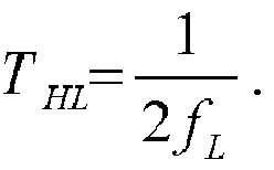
line cycle T HL 213 of the acinput voltage V AC 202 is denoted as the length of time between consecutive zero-crossings. - For leading edge dimming, the
dimmer circuit 104 disconnects the acinput voltage V AC 202 from the power converter when the acinput voltage V AC 202 substantially crosses zero voltage. After a given amount of time, thedimmer circuit 104 reconnects the acinput voltage V AC 202 with thepower converter 100 and the dimmeroutput voltage V DO 206 substantially follows the acinput voltage V AC 202. In other words, thedimmer circuit 104 disconnects theac input voltage 202 for a portion of the half line cycle to provide the dimmeroutput voltage V DO 206 thus limiting the amount of voltage and current supplied to a load (such as an LED lamp). Therectifier circuit 104 rectifies the dimmeroutput voltage V DO 206 thus providing the rectifiedvoltage V RECT 210 as shown. For the example ofFIG. 2 , the beginning of each halfline cycle T HL 202 of the rectifiedvoltage V RECT 210 is substantially equal to zero voltage corresponding to when thedimmer circuit 104 disconnects the acinput voltage V AC 202 from the power converter. When thedimmer circuit 104 reconnects the acinput voltage V AC 102 to the power converter, the rectifiedvoltage V RECT 210 substantially follows the positive magnitude of the dimmeroutput voltage V DO 206 and the acinput voltage V AC 202. Or mathematically: VRECT = |VDO |. As shown the dimmeroutput voltage V DO 206 sharply increases (or decreases) to substantially follow the acinput voltage V AC 202. The sharp increase is also illustrated in the example waveform of the rectifiedvoltage V RECT 210. The sharp increase may be referred to as the "edge." - Referring next to
FIG. 3A , example waveforms of the rectifiedvoltage V RECT 310,system clock 360, and thecount signal U COUNT 362 of the switchingpower converter 100 are illustrated including halfline cycle T HL 313,system period T SYS 374, and times t1-t5. Further,FIG. 3B illustrates the rectifiedvoltage V RECT 310,system clock 360, and thecount signal U COUNT 362 for theportion 372 ofFIG. 3A . It should be appreciated that only one halfline cycle T HL 313 is illustrated for clarity. -
FIG. 3A illustrates one halfline cycle T HL 313 of the rectifiedvoltage V RECT 310,system clock 360, and thecount signal U COUNT 362 when the dimmer circuit is not disconnecting a portion of the acinput voltage V AC 102 from thepower converter 100. Although only one halfline cycle T HL 313 is shown, the rectifiedvoltage V RECT 310 has a substantially sinusoidal shape with no edges. Thesystem clock 360 is shown as a rectangular pulse waveform with logic high and logic low sections. In the example shown, the period of thesystem clock T SYS 374 is shorter than the one halfline cycle T HL 313. Or in other words, the frequency of thesystem clock 360 is faster than the line frequency of the acinput voltage V AC 102.FIG. 3A illustrates thesystem clock 360 as notches to demonstrate that thesystem period T SYS 374 is shorter than the full and half line cycle. In one example, the full line cycle TFL 311 is 4096 times greater than thesystem period T SYS 374 of thesystem clock 360. -
Count signal U COUNT 362 is a rectangular pulse waveform which may have multiple values, in the illustrated embodiment. In the alternative,U COUNT 362 may be a digital number broadcasted as a digital word. In one example, thecount signal U COUNT 362 may be an analog representation of a digital number. For example, the value (or magnitude) of thecount signal U COUNT 362 may correspond to a digital number. As illustrated, thecount signal U COUNT 362 substantially follows the rectifiedvoltage V RECT 310 or at least a scaled-down version of VRECT 310 (e.g. input sense signal 154). In one example, thecount signal U COUNT 362 increases and decreases such that thecount signal U COUNT 362 crosses the rectifiedvoltage V RECT 310 within a given amount of time. The given amount of time may be N number of consecutivesystem periods T SYS 374. In other words, thecount signal U COUNT 362 substantially tracks the rectifiedvoltage V RECT 310 if thecount signal U COUNT 362 crosses the rectifiedvoltage V RECT 310 within N number of consecutivesystem periods T SYS 374. In one example, N may be substantially equal to 10. -
FIG. 3B illustrates theportion 372 ofFIG. 3A . As shown inFIG. 3B , thecount signal U COUNT 362 may cross the rectifiedvoltage V RECT 310 several times. In the example shown, times t1-t5 correspond to the rising edges of thesystem clock 360 and the time between rising edges is substantially thesystem period T SYS 374. At time t1 of thesystem clock 360, the value ofcount signal U COUNT 362 is less than rectifiedvoltage V RECT 310.Comparator 138 gives compare signal 164 a second state (e.g. logic high) whenU COUNT 362 is less thanV RECT 310. Thecount module 140 then increments thecount signal U COUNT 362 in response to compare signal 164 having the second state and the value of thecount signal U COUNT 362 increases and crosses rectifiedvoltage V RECT 310. At time t2 of thesystem clock 360, the value of thecount signal U COUNT 362 is greater than the rectifiedvoltage V RECT 310. As such,comparator 138 gives compare signal 164 a first state (e.g. logic low) whenU COUNT 362 is greater thanV RECT 310.Count module 140 decrements thecount signal U COUNT 362 in response to compare signal 164 having the first state and the value of thecount signal U COUNT 362 decreases and crosses the rectifiedvoltage V RECT 310. In one example, the amounts which thecount signal U COUNT 362 increases and decreases may be fixed and the resultant value after each increase and decrease may correspond to a digital count. - At time t3 of the
system clock 360, the value of thecount signal U COUNT 362 is less than the rectifiedvoltage V RECT 310. As such, the value of thecount signal U COUNT 362 is increased in response to compare signal 164 having the second state. However, the value of thecount signal U COUNT 362 at next system clock period (shown as time t4) is still less than the rectifiedvoltage V RECT 310.Count module 140 further increments thecount signal U COUNT 362 and the value of thecount signal U COUNT 362 increases to the next value. At time t4, thecount signal U COUNT 362 crosses rectifiedvoltage V RECT 310. At the next system clock period (shown as time t5), the value of thecount signal U COUNT 362 is greater than the rectifiedvoltage V RECT 310 and the value of thecount signal U COUNT 362 decreases. As shown at time t5, thecount signal U COUNT 362 crosses rectifiedvoltage V RECT 310. In the example shown inFIG. 3B , thecount signal U COUNT 362 does not cross the rectifiedvoltage V RECT 310 for two consecutiveswitching periods T SYS 374 of the system clock. As mentioned above, thecount signal U COUNT 362 substantially tracks the rectifiedvoltage V RECT 310 if thecount signal U COUNT 362 crosses the rectifiedvoltage V RECT 310 within N number of consecutivesystem periods T SYS 374. In the example where N is substantially equal to 10, thecount signal U COUNT 362 illustrated inFIG. 3B is still tracking the rectifiedvoltage V RECT 310 or at least a scaled version of VRECT 310 (e.g. input sense signal 154) since the number of consecutive switching periods which thecount signal U COUNT 362 does not cross the rectified voltage VRECT 310 (i.e. 2) is less than 10. - Referring next to
FIG. 4A , example waveforms of the rectifiedvoltage V RECT 410,system clock 460, and thecount signal U COUNT 462 of the switchingpower converter 100 are illustrated including halfline cycle T HL 413 and the system period TSYS 474.FIG.4A illustrates the example rectifiedvoltage V RECT 410 for a leading edge dimmer circuit. - The beginning of each half
line cycle T HL 413 of the rectifiedvoltage V RECT 410 is substantially equal to zero voltage corresponding to when thedimmer circuit 104 disconnects the acinput voltage V AC 102 from thepower converter 100. When thedimmer circuit 104 reconnects theac voltage V AC 102 to thepower converter 100, the rectifiedvoltage V RECT 410 substantially follows the positive magnitude of the acinput voltage V AC 102. Similar toFIGS. 3A and 3B , thecount signal U COUNT 462 is a rectangular pulse waveform with multiple values. As shown, thecount signal U COUNT 462 may partially track the rectifiedvoltage V RECT 410. However, at the leading edge of the rectified voltage VRECT 410 (when the rectifiedvoltage V RECT 410 increases from substantially zero to follow the positive magnitude of the ac input voltage VAC 102), thecount signal U COUNT 462 is unable to track the rectifiedvoltage V RECT 410. As illustrated, thecount signal U COUNT 462 is less than the rectifiedvoltage V RECT 410 for multiple periods of thesystem clock 460. In the illustrated example, thecount signal U COUNT 462 is less than the rectifiedvoltage V RECT 410 for fourteen consecutive periods of thesystem clock 460. As such, thecount module 140 increments thecount signal U COUNT 462 for fourteen consecutive periods and the value of thecount signal U COUNT 462 increases for fourteen consecutive periods of thesystem clock 460. In other words, thecount signal U COUNT 462 does not cross the rectifiedvoltage V RECT 410 within N consecutive periods of thesystem clock 460 and an edge is detected. In one example, thecount signal U COUNT 462 increasing for N or more consecutive system periods would correspond to a detected leading edge. The number of consecutive periods of the clock signal which thecount signal U COUNT 462 is less than the rectifiedvoltage V RECT 410 may be referred to as the leading edge count. - Referring next to
FIG. 4B , example waveforms of the rectifiedvoltage V RECT 410,system clock 460, and thecount signal U COUNT 462 of the switchingpower converter 100 are illustrated including halfline cycle T HL 413 and the system period TSYS 474.FIG.4B illustrates the example rectifiedvoltage V RECT 410 for a trailing edge dimmer circuit. -
FIG. 4B is similar toFIG. 4A , however thedimmer circuit 104 connects the input to thepower converter 100 to the acinput voltage V AC 102 when the acinput voltage V AC 102 crosses zero voltage and after a given amount of time, thedimmer circuit 104 then disconnects the acinput voltage V AC 102 for the remainder of the halfline cycle T HL 413. At the beginning of the halfline cycle T HL 413, the rectifiedvoltage V RECT 410 substantially follows the positive magnitude of the acinput voltage V AC 102 until thedimmer circuit 104 disconnects the acinput voltage V AC 102 from thepower converter 100. The value of the rectifiedvoltage V RECT 410 then falls to substantially zero voltage until the beginning of the next half line cycle. The decrease of the rectifiedvoltage V RECT 410 may be referred to as the trailing edge. As shown, thecount signal U COUNT 462 may partially track the rectifiedvoltage V RECT 410. However, at the trailing edge of the rectifiedvoltage V RECT 410, thecount signal U COUNT 462 is unable to track the rectifiedvoltage V RECT 410. As illustrated, thecount signal U COUNT 462 is greater than the rectifiedvoltage V RECT 410 for multiple periods of thesystem clock 460. In the illustrated example, thecount signal U COUNT 462 is greater than the rectifiedvoltage V RECT 410 for fifteen consecutive periods of thesystem clock 460. As such, thecount module 140 decrements thecount signal U COUNT 462 for fifteen consecutive periods and the value of thecount signal U COUNT 462 decreases for fourteen consecutive periods of thesystem clock 460. In other words, thecount signal U COUNT 462 does not cross the rectifiedvoltage V RECT 410 within N consecutive periods of thesystem clock 460 and an edge is detected. In one example, thecount signal U COUNT 462 decreasing for N or more consecutive system periods would correspond to a detected trailing edge. The number of consecutive periods of the clock signal which thecount signal U COUNT 462 is greater than the rectifiedvoltage V RECT 410 may be referred to as the trailing edge count. -
FIG. 5 is a flow diagram illustrating anexample process 500 for detecting an edge in an input waveform in accordance with an example of the present invention. The order in which some or all of the process blocks appear inprocess 500 should not be deemed limiting. Rather, one of ordinary skill in the art having the benefit of the present disclosure will understand that some of the process blocks may be executed in a variety of orders not illustrated, or even in parallel. - In
process block 505, the voltage sense signal (e.g. voltage sense signal 154) is compared with the count signal UCOUNT (e.g. count signal UCOUNT 162). Inprocess block 510,process 500 determines whether the count signal UCOUNT is greater than the voltage sense signal. If the count signal UCOUNT is greater than the voltage sense signal, the process moves to block 515 and the count signal UCOUNT is decremented or decreased. However, if the count signal UCOUNT is not greater than the voltage sense signal, the process moves to block 520 and the count signal is UCOUNT incremented or increased. - At
block 525, if the count signal UCOUNT is incremented, a leading edge count is also incremented (or increased) and a trailing edge count is reset to substantially zero. Atblock 530, if the count signal UCOUNT is decremented, a leading edge count is reset to substantially zero and the trailing edge count is incremented (or increased). Atblock 535, the process determines if the leading edge count is greater than the first threshold (e.g. ten). If the leading edge count is not greater than the first threshold, the process returns to block 505. If the leading edge count is greater than the first threshold, the process asserts the leading edge confirmed signal (e.g. leading edge signal ULE 167) inblock 545. - At
block 540, the process determines if the trailing edge count is greater than the second threshold (e.g. 10). If the trailing edge count is not greater than the second threshold, the process returns to block 505. If the trailing edge count is greater than the second threshold, the process asserts the trailing edge confirmed signal (e.g. trailing edge signal UTE 168) inblock 550. It should be appreciated that the first threshold and the second threshold may correspond to the N number of consecutive periods of the system clock which the count signal is unable to track the rectified voltage. In addition, the first threshold and the second threshold may be the same threshold. -
FIG. 6 illustrates an exampleedge detection circuit 636 including acount module 640, leadingedge check circuit 642, trailingedge check circuit 644, aresistor 674, a currentmirror including transistors driver 678.Count module 640 is shown including acounter 679 and anM bit DAC 681. Leadingedge check circuit 642 includes counter 682 anddigital comparator 683. In addition, trailingedge check circuit 644 includes counter 684 anddigital comparator 685.FIG. 6 also includes inputvoltage sense signal 654, input voltage sense current IVIN 675, count signal ICOUNT 662,system clock 660, comparator output 664 (i.e. compare signal 664), leadingedge signal U LE 667 and trailingedge signal U TE 668, first threshold TH1 691, andsecond threshold TH2 692. - In one example, input
voltage sense signal 654 may be a voltage signal. Theresistor 674 is coupled to receive the inputvoltage sense signal 654 and convert the voltage signal to a current signal, shown as input voltage sensecurrent I VIN 675.Transistors first transistor 676 is coupled to receive the input voltage sense current IVIN 675 and the input voltage sense current IVIN 675 is mirrored to thesecond transistor 677. - For the example of
FIG. 6 , the count signal UCOUNT is exemplified as a current signal,count signal I COUNT 662. Thecomparator 138 is exemplified by the terminal 638 since both the count signal ICOUNT 662 and the input voltage sense current IVIN 675 are current signals. One end ofdriver 678 is coupled to the terminal 638 and the output 664 (compare signal 664) of thedriver 678 is received atcounters signal 664 is received at the UP/DOWN input ofcounter 679 and is received at the COUNT/RESET inputs ofcounters FIG. 6 , each ofcounters system clock 660 at their clock inputs. - In one example, the output of
counter 679 is a digital word of M length and is referred to asdigital count U DC 680. Thedigital count U DC 680 is coupled to be received by theM bit DAC 681 which converters thedigital count U DC 680 to an analog signal. As illustrated, thedigital count U DC 680 is converted to the count signal ICOUNT 662 where magnitudes of the count signal ICOUNT 662 correspond to a specific count of thedigital count U DC 680. - The outputs of
counters digital comparators digital comparators second threshold TH2 692, respectively. As will be further discussed,digital comparator 683 is coupled to compare the output ofcounter 682 with the first threshold TH1 691. The output ofdigital comparator 683 is the leadingedge signal U LE 667. A logic high value of the leadingedge signal U LE 667 may correspond to the output ofcounter 682 being greater than the first threshold TH1 691while a logic low value may correspond to the output ofcounter 682 being less than the first threshold TH1 691. - Similarly, the
digital comparator 685 compares the output of thecounter 684 with thesecond threshold TH2 692. The output of thedigital comparator 685 is the trailingedge signal U TE 668. A logic high value of the trailingedge signal U TE 668 may correspond to the output ofcounter 684 being greater than the second threshold TH2 692while a logic low value may correspond to the output ofcounter 684 being less than thesecond threshold TH2 692. - In operation, the input voltage sense current IVIN 675 is compared to the count signal ICOUNT 662 at
terminal 638. In one example, if the input voltage sense current IVIN 675 is greater than the count signal ICOUNT 662, the voltage atterminal 638 is pulled high. The output 664 (count signal 664) of thedriver 678 is a logic high value and the value stored incounter 679 is incremented. If the count signal ICOUNT 662 is greater than the input voltage sense current IVIN 675, the voltage atterminal 638 is pulled low and the output 664 (compare signal 664) of the driver is a logic low value and the value stored incounter 679 is decremented. - When
counter 679 receives a logic high value, the value of thedigital count U DC 680 is incremented. When thecounter 679 receives a logic low value, the value of thedigital count U DC 680 is decremented. TheM bit DAC 681 converts thedigital count U DC 680 to an analogcount signal I COUNT 662. - In one example, counter 682 of the leading
edge check circuit 642 increments when theoutput 664 is logic high and resets when theoutput 664 is logic low. As such, the value of thecounter 682 increases with every consecutive period of the system clock which the input voltage sense current IVIN 675 is greater than thecount signal I COUNT 662. The output of thecounter 682 is compared to a first threshold TH1 691. Thedigital comparator 683 outputs a logic high value when the output ofcounter 682 is greater than the first threshold TH1 691 and a logic low value otherwise. - Further, in one example the
counter 684 of the trailingedge check circuit 644 increments when theoutput 664 is logic low and resets when theoutput 664 is logic high. As such, the value of thecounter 682 increases with every consecutive period of the system clock which the count signal ICOUNT 662 is greater than the input voltage sensecurrent I VIN 675. The output of thecounter 684 is compared to asecond threshold TH2 692. Thedigital comparator 685 outputs a logic high value when the output ofcounter 684 is greater than thesecond threshold TH2 692 and a logic low value otherwise. -
FIG. 7 illustrates an example leading edge check circuit 742 and trailing edge check circuit 744 including ashift register 786,decoder 788,digital comparator 790, anddigital comparator 789.FIG. 7 also includessystem clock 760, comparesignal 764, the leadingedge signal U LE 767, the trailingedge signal U TE 768, anupper threshold THU 793, and alower threshold THL 794. -
Shift register 786 is coupled to receive the comparesignal 764 and thesystem clock 760 and also coupled to thedecoder 788. As mentioned above, the comparesignal 764 may be logic high or logic low depending on whether the input signal is greater than the count signal.Shift register 786 may include L number of registers (illustrated as P1, P2, P3, P4, PL) which may store L number of values of the comparesignal 764. In one example, each register (P1, P2, P3, P4, PL) of theshift register 786 may be a one bit register. The values stored in each individual register of theshift register 786 may be received by thedecoder 788. In one example, thedecoder 788 may determine the number of (logic) ones stored in theshift register 786. Alternatively, the decoder may determine the number of (logic) zeros stored in theshift register 786.Digital comparators decoder 788. The output of thedigital comparator 790 is the leadingedge signal U LE 767 while the output ofdigital comparator 789 is the trailingedge signal U TE 768. The leadingedge signal U LE 767 and the trailingedge signal U TE 768 may be rectangular pulse waveforms with varying lengths of logic high and logic low sections. In one example, the leadingedge signal U LE 767 may be logic high when a leading edge is detected or may pulse to a logic high value when a leading edge is detected. Further, in one example the trailingedge signal U TE 768 may be logic high when a trailing edge is detected or may pulse to a logic high value when a trailing edge is detected. - In operation, the individual registers of the
shift register 786 are prestored with alternating logic high and logic low values (e.g. ones or zeros). For example, register P1 may be stored with a logic zero while register P2 is stored with a logic one and so on until register PL is stored with a logic one (if L is an even number) or a logic zero (if L is an odd number). In one example, L may be 32 and theshift register 786 is initially stored with alternating 16 logic zeros and 16 logic ones. As theshift register 786 updates (in response to the system clock 760), theshift register 786 stores the next value provided by the comparesignal 764. Thedecoder 788 determines the number of logic ones (or logic zeros) stored in theshift register 786 and outputs the total number of logic ones (or logic zeros). Thedigital comparator 790 compares the total number of logic ones determined by thedecoder 788 with theupper threshold THU 793 and asserts the leadingedge signal U LE 767 when the total number of logic ones are greater than theupper threshold THU 793.Digital comparator 789 compares the output of the decoder 788 (total number of logic ones) with thelower threshold THL 794 and asserts the trailingedge signal UTE 768 when the total number of logic ones are less than thelower threshold THL 794. In an example, the value of thelower threshold THL 794 is less than theupper threshold THU 793. - In some examples, when the dimmer circuit (e.g. dimmer circuit 104) begins conducting, the input voltage may ring and change directions multiple times which may lead to a missed detection of the edge. In one example, the leading edge check circuit 742 and the trailing edge check circuit 744 monitors the density of logic one values. In other words, the leading edge check circuit 742 monitors the total number of logic one values stored within the
shift register 786. If the total number of logic ones is greater than an upper threshold, a leading edge is detected. If the total number of logic ones is less than a lower threshold, a trailing edge is detected. Alternatively, the leading edge check circuit 742 and the trailing edge check circuit 744 may monitor the density of logic zero values. In other words, the trailing edge check circuit monitors the total number of logic zero values stored within the shift register and if the total number of logic zeros is greater than an upper threshold, a trailing edge is detected. However, if the total number of logic zeros is less than a lower threshold, a leading edge is detected. In both examples, the value of the lower threshold is less than the upper threshold. - The above description of illustrated examples of the present invention, including what is described in the Abstract, are not intended to be exhaustive or to be limitation to the precise forms disclosed. While specific embodiments of, and examples for, the invention are described herein for illustrative purposes, various equivalent modifications are possible without departing from the broader spirit and scope of the present invention. Indeed, it is appreciated that the specific example voltages, currents, frequencies, power range values, times, etc., are provided for explanation purposes and that other values may also be employed in other embodiments and examples in accordance with the teachings of the present invention.
- Although the present invention is defined in the attached claims, it should be understood that the present invention can also (alternatively) be defined in accordance with the following embodiments:
- 1. A controller for a power converter, the controller comprising:
- an edge detection circuit including:
- a comparator coupled to output a compare signal in response to comparing an input sense signal and a count signal, wherein the comparator gives the compare signal a first state when the input sense signal is below the count signal and gives the compare signal a second state when the input sense signal is above the count signal, the input sense signal representative of an input voltage of the power converter;
- a count module coupled to adjust the count signal to track the input sense signal in response to receiving the compare signal; and
- an edge checking module coupled to output at least one edge signal in response to the compare signal not changing between the first and the second state for a given time period; and
- a drive circuit coupled to output a drive signal in response to the at least one edge signal, wherein the drive signal is for controlling a switch coupled to regulate an output of the power converter.
- an edge detection circuit including:
- 2. The controller of
embodiment 1, wherein the count module decreases the count signal when the compare signal has the first state, and wherein the count module increases the count signal when the compare signal has the second state. - 3. The controller of
embodiment 1, wherein the edge checking module includes a trailing edge block coupled to output a trailing edge signal when the compare signal is at the first state for at least the given time period, the at least one edge signal including the trailing edge signal. - 4. The controller of embodiment 3, wherein the trailing edge block includes:
- a first counter coupled to output a first counter output in response to the compare signal, wherein the first counter output is periodically incremented when the compare signal is at the first state, and wherein the first counter output is reset when the compare signal changes from the first state to the second state; and
- a first digital comparator coupled to assert the trailing edge signal when the first counter output reaches a given threshold representative of the given time period, wherein the given threshold is an integer.
- 5. The controller of
embodiment 1, wherein the edge checking module includes a leading edge block coupled to output a leading edge signal when the compare signal is at the second state for at least the given time period, the at least one edge signal including the leading edge signal. - 6. The controller of embodiment 5, wherein the leading edge block includes:
- a second counter coupled to output a second counter output in response to the compare signal, wherein the second counter output is periodically incremented when the compare signal is at the second state, and wherein the second counter output is reset when the compare signal changes from the second state to the first state; and
- a second digital comparator coupled to assert the leading edge signal when the second counter output reaches a given threshold representative of the given time period, wherein the given threshold is an integer.
- 7. The controller of
embodiment 1 further comprising an oscillator coupled to generate a system clock, wherein the count module and the edge checking module are coupled to receive the system clock, and wherein the count module adjusts the count signal in response to the system clock. - 8. The controller of embodiment 7, wherein the given time period is ten cycles of the system clock.
- 9. The controller of
embodiment 1, wherein the count module includes a counter coupled to output a digital word of N length in response to the compare signal, the count module further including a digital-to-analog converter ("DAC") coupled to output the count signal in response to the digital word, wherein the count signal is an analog signal. - 10. The controller of
embodiment 1, wherein the controller and the switch are included in an integrated circuit. - 11. The controller of
embodiment 1, wherein the edge checking module includes:- a register coupled to receive the compare signal and to store L number of values of the compare signal and output the L number of values;
- a decoder coupled to receive the L number of stored values and determine a total number of the L number of values which are substantially equal to the first state; and
- a comparator coupled to receive the total number and to assert a trailing edge signal when the total number reaches a lower threshold.
- 12. The controller of
embodiment 1, wherein the edge checking module includes:- a register coupled to receive the compare signal and to store L number of values of the compare signal and output the L number of values;
- a decoder coupled to receive the L number of stored values and determine a total number of the L number of values which are substantially equal to the second state; and
- a comparator coupled to receive the total number and to assert a leading edge signal when the total number reaches an upper threshold.
- 13. A method of operating a controller of a power converter, the method comprising:
- receiving an input sense signal;
- generating a compare signal based on a comparison of the input sense signal and a count signal;
- adjusting the count signal to track the input sense signal, wherein the adjusting is based on the compare signal; and
- outputting at least one edge signal in response to the compare signal not changing states for a given time period, wherein a switch coupled to regulate an output of the power converter is responsive to the at least one edge signal.
- 14. The method of
embodiment 13, wherein the compare signal has a first state when the input sense signal is below the count signal, and wherein the compare signal has a second state when the input sense signal is above the count signal, and further wherein said adjusting the count signal includes decreasing the count signal when the compare signal has a first state and increasing the count signal when the compare signal has a second state. - 15. The method of
embodiment 14, wherein a trailing edge signal is outputted when the compare signal is at the first state for at least the given time period, the at least one edge signal including the trailing edge signal, and wherein outputting the trailing edge signal indicates that a leading edge dimmer is providing the input sense signal. - 16. The method of
embodiment 14, wherein a leading edge signal is outputted when the compare signal is at the second state for at least the given time period, the at least one edge signal including the leading edge signal, and wherein outputting the leading edge signal indicates that a trailing edge dimmer is providing the input sense signal. - 17. The method of
embodiment 13, wherein the given time period is an integer number of cycles of a clock. - 18. A switched mode power converter comprising:
- a switch;
- an energy transfer element coupled to the switch and coupled to receive an input sense signal; and
- a controller coupled to the switch to regulate an output of the switched mode power converter in response to a dimming signal, wherein the controller includes:
- an edge detection circuit including:
- a comparator coupled to output a compare signal in response to comparing the dimming signal and a count signal, wherein the comparator gives the compare signal a first state when the dimming signal is below the count signal and gives the compare signal a second state when the dimming signal is above the count signal, the dimming signal representative of an input voltage of the switched mode power converter;
- a count module coupled to adjust the count signal to track the dimming signal in response to receiving the compare signal; and
- an edge checking module coupled to output at least one edge signal in response to the compare signal not changing between the first and the second state for a given time period; and
- an edge detection circuit including:
- a drive circuit coupled to output a drive signal in response to the at least one edge signal, wherein the drive signal is for controlling a switch coupled to regulate an output of the switched mode power converter.
- 19. The switched mode power converter of embodiment 18, wherein the count module decreases the count signal when the compare signal has the first state, and wherein the count module increases the count signal when the compare signal has the second state.
- 20. The switched mode power converter of embodiment 18, wherein the edge checking module includes a trailing edge block coupled to output a trailing edge signal when the compare signal is at the first state for the given time period, the at least one edge signal including the trailing edge signal.
- 21. The switched mode power converter of embodiment 18, wherein the edge checking module includes a leading edge block coupled to output a leading edge signal when the compare signal is at the second state for the given time period, the at least one edge signal including the leading edge signal.
- 22. The switched mode power converter of embodiment 18, wherein the edge checking module includes:
- a register coupled to receive the compare signal and to store L number of values of the compare signal and output the L number of values;
- a decoder coupled to receive the L number of stored values and determine a total number of the L number of values which are substantially equal to the first state; and
- a comparator coupled to receive the total number and to assert a trailing edge signal when the total number reaches a lower threshold.
- 23. The switched mode power converter of embodiment 18, wherein the edge checking module includes:
- a register coupled to receive the compare signal and to store L number of values of the compare signal and output the L number of values;
- a decoder coupled to receive the L number of stored values and determine a total number of the L number of values which are substantially equal to the second state; and
- a comparator coupled to receive the total number and to assert a leading edge signal when the total number reaches an upper threshold.
Claims (15)
- A controller for a power converter, the controller comprising:an edge detection circuit including:a comparator coupled to output a compare signal in response to comparing an input sense signal and a count signal, wherein the comparator gives the compare signal a first state when the input sense signal is below the count signal and gives the compare signal a second state when the input sense signal is above the count signal, the input sense signal representative of an input voltage of the power converter;a count module coupled to adjust the count signal to track the input sense signal in response to receiving the compare signal; andan edge checking module coupled to output at least one edge signal in response to the compare signal not changing between the first and the second state for a given time period; anda drive circuit coupled to output a drive signal in response to the at least one edge signal, wherein the drive signal is for controlling a switch coupled to regulate an output of the power converter.
- The controller of claim 1, wherein the count module decreases the count signal when the compare signal has the first state, and wherein the count module increases the count signal when the compare signal has the second state.
- The controller of claim 1, wherein the edge checking module includes a trailing edge block coupled to output a trailing edge signal when the compare signal is at the first state for at least the given time period, the at least one edge signal including the trailing edge signal.
- The controller of claim 3, wherein the trailing edge block includes:a first counter coupled to output a first counter output in response to the compare signal,wherein the first counter output is periodically incremented when the compare signal is at the first state, and wherein the first counter output is reset when the compare signal changes from the first state to the second state; anda first digital comparator coupled to assert the trailing edge signal when the first counter output reaches a given threshold representative of the given time period, wherein the given threshold is an integer.
- The controller of claim 1, wherein the edge checking module includes a leading edge block coupled to output a leading edge signal when the compare signal is at the second state for at least the given time period, the at least one edge signal including the leading edge signal.
- The controller of claim 5, wherein the leading edge block includes:a second counter coupled to output a second counter output in response to the compare signal, wherein the second counter output is periodically incremented when the compare signal is at the second state, and wherein the second counter output is reset when the compare signal changes from the second state to the first state; anda second digital comparator coupled to assert the leading edge signal when the second counter output reaches a given threshold representative of the given time period, wherein the given threshold is an integer.
- The controller of claim 1 further comprising an oscillator coupled to generate a system clock, wherein the count module and the edge checking module are coupled to receive the system clock, and wherein the count module adjusts the count signal in response to the system clock, for example, wherein the given time period is ten cycles of the system clock.
- The controller of claim 1, wherein the count module includes a counter coupled to output a digital word of N length in response to the compare signal, the count module further including a digital-to-analog converter ("DAC") coupled to output the count signal in response to the digital word, wherein the count signal is an analog signal.
- The controller of claim 1, wherein the edge checking module includes:a register coupled to receive the compare signal and to store L number of values of the compare signal and output the L number of values;a decoder coupled to receive the L number of stored values and determine a total number of the L number of values which are substantially equal to the first state; anda comparator coupled to receive the total number and to assert a trailing edge signal when the total number reaches a lower threshold.
- The controller of claim 1, wherein the edge checking module includes:a register coupled to receive the compare signal and to store L number of values of the compare signal and output the L number of values;a decoder coupled to receive the L number of stored values and determine a total number of the L number of values which are substantially equal to the second state; anda comparator coupled to receive the total number and to assert a leading edge signal when the total number reaches an upper threshold.
- A method of operating a controller of a power converter, the method comprising:receiving an input sense signal;generating a compare signal based on a comparison of the input sense signal and a count signal;adjusting the count signal to track the input sense signal, wherein the adjusting is based on the compare signal; andoutputting at least one edge signal in response to the compare signal not changing states for a given time period, wherein a switch coupled to regulate an output of the power converter is responsive to the at least one edge signal.
- The method of claim 11, wherein the compare signal has a first state when the input sense signal is below the count signal, and wherein the compare signal has a second state when the input sense signal is above the count signal, and further wherein said adjusting the count signal includes decreasing the count signal when the compare signal has a first state and increasing the count signal when the compare signal has a second state.
- The method of claim 12, wherein a trailing edge signal is outputted when the compare signal is at the first state for at least the given time period, the at least one edge signal including the trailing edge signal, and wherein outputting the trailing edge signal indicates that a leading edge dimmer is providing the input sense signal.
- The method of claim 12, wherein a leading edge signal is outputted when the compare signal is at the second state for at least the given time period, the at least one edge signal including the leading edge signal, and wherein outputting the leading edge signal indicates that a trailing edge dimmer is providing the input sense signal.
- A switched mode power converter comprising:a switch;an energy transfer element coupled to the switch and coupled to receive an input sense signal; andthe controller of any one of claims 1, 2, 3, 5, 11, and 12,wherein the controller is coupled to the switch to regulate an output of the switched mode power converter in response to a dimming signal representative of the input voltage of the power converter
Applications Claiming Priority (1)
| Application Number | Priority Date | Filing Date | Title |
|---|---|---|---|
| US14/259,028 US9369048B2 (en) | 2014-04-22 | 2014-04-22 | Dimming edge detection for power converter |
Publications (1)
| Publication Number | Publication Date |
|---|---|
| EP2938163A1 true EP2938163A1 (en) | 2015-10-28 |
Family
ID=52997305
Family Applications (1)
| Application Number | Title | Priority Date | Filing Date |
|---|---|---|---|
| EP15164258.4A Withdrawn EP2938163A1 (en) | 2014-04-22 | 2015-04-20 | Dimming edge detection for power converter |
Country Status (3)
| Country | Link |
|---|---|
| US (1) | US9369048B2 (en) |
| EP (1) | EP2938163A1 (en) |
| CN (1) | CN105050235B (en) |
Cited By (1)
| Publication number | Priority date | Publication date | Assignee | Title |
|---|---|---|---|---|
| WO2016077181A1 (en) * | 2014-11-10 | 2016-05-19 | Power Integrations, Inc. | Phase angle detection module for power converter |
Families Citing this family (10)
| Publication number | Priority date | Publication date | Assignee | Title |
|---|---|---|---|---|
| US9282598B2 (en) * | 2013-03-15 | 2016-03-08 | Koninklijke Philips N.V. | System and method for learning dimmer characteristics |
| US9369048B2 (en) * | 2014-04-22 | 2016-06-14 | Power Integrations, Inc. | Dimming edge detection for power converter |
| JP6481814B2 (en) * | 2015-02-19 | 2019-03-13 | 株式会社リコー | Inverter device |
| US9893630B2 (en) | 2016-02-26 | 2018-02-13 | Power Integrations, Inc. | Reduction of audible noise in a power converter |
| US9876433B2 (en) * | 2016-02-26 | 2018-01-23 | Power Integrations, Inc. | Reduction of audible noise in a power converter |
| US10763844B2 (en) * | 2018-08-28 | 2020-09-01 | Texas Instruments Incorporated | Methods and apparatus to transmit signals in isolated gate drivers |
| US10797583B2 (en) * | 2018-12-13 | 2020-10-06 | Power Integrations, Inc. | Secondary winding sense for hard switch detection |
| CN113300441B (en) * | 2021-07-28 | 2021-12-10 | 深圳赫兹创新技术有限公司 | Wireless charging derating control method, device and system with repeatedly adjusted output current |
| CN114007305A (en) * | 2021-10-09 | 2022-02-01 | 深圳南云微电子有限公司 | Control method and controller |
| US20240223082A1 (en) * | 2023-01-04 | 2024-07-04 | Texas Instruments Incorporated | Determination of values indicative of multiple passive components connected to a device pin |
Citations (2)
| Publication number | Priority date | Publication date | Assignee | Title |
|---|---|---|---|---|
| EP2387294A2 (en) * | 2010-04-30 | 2011-11-16 | Osram Gesellschaft mit beschränkter Haftung | Method and device for obtaining conduction angle, method and device for driving LED |
| WO2013114242A1 (en) * | 2012-02-01 | 2013-08-08 | Koninklijke Philips N.V. | Driver device and driving method for driving a load, in particular in led unit comprising one or more leds |
Family Cites Families (9)
| Publication number | Priority date | Publication date | Assignee | Title |
|---|---|---|---|---|
| US7471530B2 (en) * | 2006-10-04 | 2008-12-30 | Power Integrations, Inc. | Method and apparatus to reduce audio frequencies in a switching power supply |
| WO2012027507A2 (en) * | 2010-08-24 | 2012-03-01 | Cirrus Logic, Inc. | Multi-mode dimmer interfacing including attach state control |
| US9084309B2 (en) * | 2012-05-23 | 2015-07-14 | Texas Instruments Incorporated | Digital phase angle detection and processing |
| US8866525B2 (en) * | 2013-02-27 | 2014-10-21 | Microchip Technology Incorporated | Configurable time delays for equalizing pulse width modulation timing |
| CN105048822B (en) * | 2013-08-29 | 2019-03-01 | 昂宝电子(上海)有限公司 | System and method for regulating frequency and current based on load conditions |
| US9270190B2 (en) * | 2014-01-22 | 2016-02-23 | Linear Technology Corporation | Predictive and reactive control of secondary side synchronous rectifiers in forward converters |
| US9331586B2 (en) * | 2014-04-15 | 2016-05-03 | Power Integrations, Inc. | Sampling for dimmer edge detection in power converter |
| US9369048B2 (en) * | 2014-04-22 | 2016-06-14 | Power Integrations, Inc. | Dimming edge detection for power converter |
| US9214851B1 (en) * | 2014-07-02 | 2015-12-15 | Power Integrations, Inc. | Trailing edge detector using current collapse |
-
2014
- 2014-04-22 US US14/259,028 patent/US9369048B2/en not_active Expired - Fee Related
-
2015
- 2015-04-20 EP EP15164258.4A patent/EP2938163A1/en not_active Withdrawn
- 2015-04-22 CN CN201510194839.8A patent/CN105050235B/en not_active Expired - Fee Related
Patent Citations (2)
| Publication number | Priority date | Publication date | Assignee | Title |
|---|---|---|---|---|
| EP2387294A2 (en) * | 2010-04-30 | 2011-11-16 | Osram Gesellschaft mit beschränkter Haftung | Method and device for obtaining conduction angle, method and device for driving LED |
| WO2013114242A1 (en) * | 2012-02-01 | 2013-08-08 | Koninklijke Philips N.V. | Driver device and driving method for driving a load, in particular in led unit comprising one or more leds |
Cited By (2)
| Publication number | Priority date | Publication date | Assignee | Title |
|---|---|---|---|---|
| WO2016077181A1 (en) * | 2014-11-10 | 2016-05-19 | Power Integrations, Inc. | Phase angle detection module for power converter |
| US9438122B2 (en) | 2014-11-10 | 2016-09-06 | Power Integrations, Inc. | Phase angle detection module for power converter |
Also Published As
| Publication number | Publication date |
|---|---|
| CN105050235B (en) | 2019-04-02 |
| CN105050235A (en) | 2015-11-11 |
| US20150303812A1 (en) | 2015-10-22 |
| US9369048B2 (en) | 2016-06-14 |
Similar Documents
| Publication | Publication Date | Title |
|---|---|---|
| US9369048B2 (en) | Dimming edge detection for power converter | |
| EP2963999B1 (en) | Trailing edge detector using current collapse | |
| EP2381742B1 (en) | Dimming control for a switching power supply | |
| US8102683B2 (en) | Phase angle measurement of a dimming circuit for a switching power supply | |
| US8553439B2 (en) | Method and apparatus for determining zero-crossing of an AC input voltage to a power supply | |
| US9473031B2 (en) | Variable feedback signal based on conduction time | |
| US9680382B2 (en) | Input frequency measurement | |
| EP2393189A2 (en) | Integrated on-time extension for non-dissipative bleeding in a power supply | |
| US9572224B2 (en) | Bleeder protection using thermal foldback | |
| US9438122B2 (en) | Phase angle detection module for power converter | |
| US9331586B2 (en) | Sampling for dimmer edge detection in power converter |
Legal Events
| Date | Code | Title | Description |
|---|---|---|---|
| PUAI | Public reference made under article 153(3) epc to a published international application that has entered the european phase |
Free format text: ORIGINAL CODE: 0009012 |
|
| 17P | Request for examination filed |
Effective date: 20150420 |
|
| AK | Designated contracting states |
Kind code of ref document: A1 Designated state(s): AL AT BE BG CH CY CZ DE DK EE ES FI FR GB GR HR HU IE IS IT LI LT LU LV MC MK MT NL NO PL PT RO RS SE SI SK SM TR |
|
| AX | Request for extension of the european patent |
Extension state: BA ME |
|
| STAA | Information on the status of an ep patent application or granted ep patent |
Free format text: STATUS: THE APPLICATION IS DEEMED TO BE WITHDRAWN |
|
| 18D | Application deemed to be withdrawn |
Effective date: 20171103 |