EP2933828A1 - Method for transferring a useful layer - Google Patents
Method for transferring a useful layer Download PDFInfo
- Publication number
- EP2933828A1 EP2933828A1 EP15162329.5A EP15162329A EP2933828A1 EP 2933828 A1 EP2933828 A1 EP 2933828A1 EP 15162329 A EP15162329 A EP 15162329A EP 2933828 A1 EP2933828 A1 EP 2933828A1
- Authority
- EP
- European Patent Office
- Prior art keywords
- assembly
- fractured
- absorbent element
- substrate
- initiation
- Prior art date
- Legal status (The legal status is an assumption and is not a legal conclusion. Google has not performed a legal analysis and makes no representation as to the accuracy of the status listed.)
- Granted
Links
Images


Classifications
-
- H—ELECTRICITY
- H10—SEMICONDUCTOR DEVICES; ELECTRIC SOLID-STATE DEVICES NOT OTHERWISE PROVIDED FOR
- H10P—GENERIC PROCESSES OR APPARATUS FOR THE MANUFACTURE OR TREATMENT OF DEVICES COVERED BY CLASS H10
- H10P90/00—Preparation of wafers not covered by a single main group of this subclass, e.g. wafer reinforcement
- H10P90/19—Preparing inhomogeneous wafers
- H10P90/1904—Preparing vertically inhomogeneous wafers
- H10P90/1906—Preparing SOI wafers
- H10P90/1914—Preparing SOI wafers using bonding
- H10P90/1916—Preparing SOI wafers using bonding with separation or delamination along an ion implanted layer, e.g. Smart-cut
-
- H—ELECTRICITY
- H10—SEMICONDUCTOR DEVICES; ELECTRIC SOLID-STATE DEVICES NOT OTHERWISE PROVIDED FOR
- H10P—GENERIC PROCESSES OR APPARATUS FOR THE MANUFACTURE OR TREATMENT OF DEVICES COVERED BY CLASS H10
- H10P54/00—Cutting or separating of wafers, substrates or parts of devices
- H10P54/50—Cutting or separating of wafers, substrates or parts of devices by scoring, breaking or cleaving
- H10P54/52—Cutting or separating of wafers, substrates or parts of devices by scoring, breaking or cleaving by cleaving
-
- H—ELECTRICITY
- H10—SEMICONDUCTOR DEVICES; ELECTRIC SOLID-STATE DEVICES NOT OTHERWISE PROVIDED FOR
- H10P—GENERIC PROCESSES OR APPARATUS FOR THE MANUFACTURE OR TREATMENT OF DEVICES COVERED BY CLASS H10
- H10P72/00—Handling or holding of wafers, substrates or devices during manufacture or treatment thereof
- H10P72/70—Handling or holding of wafers, substrates or devices during manufacture or treatment thereof for supporting or gripping
- H10P72/74—Handling or holding of wafers, substrates or devices during manufacture or treatment thereof for supporting or gripping using temporarily an auxiliary support
-
- H—ELECTRICITY
- H10—SEMICONDUCTOR DEVICES; ELECTRIC SOLID-STATE DEVICES NOT OTHERWISE PROVIDED FOR
- H10W—GENERIC PACKAGES, INTERCONNECTIONS, CONNECTORS OR OTHER CONSTRUCTIONAL DETAILS OF DEVICES COVERED BY CLASS H10
- H10W10/00—Isolation regions in semiconductor bodies between components of integrated devices
- H10W10/10—Isolation regions comprising dielectric materials
- H10W10/181—Semiconductor-on-insulator [SOI] isolation regions, e.g. buried oxide regions of SOI wafers
-
- H—ELECTRICITY
- H10—SEMICONDUCTOR DEVICES; ELECTRIC SOLID-STATE DEVICES NOT OTHERWISE PROVIDED FOR
- H10P—GENERIC PROCESSES OR APPARATUS FOR THE MANUFACTURE OR TREATMENT OF DEVICES COVERED BY CLASS H10
- H10P72/00—Handling or holding of wafers, substrates or devices during manufacture or treatment thereof
- H10P72/70—Handling or holding of wafers, substrates or devices during manufacture or treatment thereof for supporting or gripping
- H10P72/74—Handling or holding of wafers, substrates or devices during manufacture or treatment thereof for supporting or gripping using temporarily an auxiliary support
- H10P72/7432—Handling or holding of wafers, substrates or devices during manufacture or treatment thereof for supporting or gripping using temporarily an auxiliary support used in a transfer process involving transfer directly from an origin substrate to a target substrate without use of an intermediate handle substrate
-
- H—ELECTRICITY
- H10—SEMICONDUCTOR DEVICES; ELECTRIC SOLID-STATE DEVICES NOT OTHERWISE PROVIDED FOR
- H10P—GENERIC PROCESSES OR APPARATUS FOR THE MANUFACTURE OR TREATMENT OF DEVICES COVERED BY CLASS H10
- H10P72/00—Handling or holding of wafers, substrates or devices during manufacture or treatment thereof
- H10P72/70—Handling or holding of wafers, substrates or devices during manufacture or treatment thereof for supporting or gripping
- H10P72/74—Handling or holding of wafers, substrates or devices during manufacture or treatment thereof for supporting or gripping using temporarily an auxiliary support
- H10P72/744—Details of chemical or physical process used for separating the auxiliary support from a device or a wafer
Definitions
- the present invention relates to a method for transferring a useful layer onto a supporting substrate.
- a method for transferring a useful layer 3 onto a supporting substrate 4, shown in Figure 1 is known from the prior art, this method including the following main steps:
- the implanted species cause the development of microcavities.
- the effect of the thermal fragilization treatment is to promote the coalescence and pressurization of these microcavities. Under the effect of this thermal treatment alone, or through additional external forces, the initiation and self-sustained propagation of a fracture wave enables the transfer of the useful layer 3 through detachment in the fragilization plane 2.
- the first substrate 1 and the support 4 are formed from a silicon wafer, and one or the other of the first substrate 1 and the support 4 are surface-oxidized.
- These silicon-on-insulator substrates must comply with very precise specifications. This applies in particular to the average thickness and uniformity of thickness of the useful layer 3. Compliance with these specifications is required for the correct operation of the semiconductor devices that will be formed in or on this useful layer 3.
- the architecture of these semiconductor devices requires the provision of silicon-on-insulator substrates having a very low average thickness of the useful layer 3, for example less than 50 nm, or even less than 10 nm, and a uniformity of thickness that is highly constant on the surface of the substrate (the normalized diameter of which is typically 200 mm, 300 mm, and even 450 mm for the next generations).
- the expected uniformity of thickness may thus be in the order of at most 1%, corresponding to variation maxima typically ranging from +/0.1 nm to +/-1 nm over the entire surface of the wafer.
- One object of the invention is to propose a method for transferring a useful layer onto a support substrate, this useful layer having a periodic pattern of thickness variation, the size of which is reduced.
- the inventors of the present application found that the initiation and/or propagation of the fracture wave was liable to cause this assembly to vibrate.
- These Lamb-wave vibrations propagate without significant attenuation over distances comparable to the size of the substrates, and at a speed greater than the speed of the self-sustained fracture wave. They are reflected, once or several times, on the ends of the assembly to be fractured, which helps to maintain this acoustic vibration in the assembly during the propagation of the fracture wave.
- the inventors have thus found that the modulation of the fracture wave by these acoustic vibrations was the cause of the periodic pattern of thickness variation observed on the useful layer at the end of the method.
- the subject-matter of the invention proposes a method for transferring a useful layer onto a support including the following steps of:
- At least one of the sides of the assembly to be fractured is in close contact, over a contact zone, with an absorbent element suitable for capturing and dissipating the acoustic vibrations emitted during the initiation and/or propagation of the fracture wave.
- the absorbent element Since at least some of the emitted acoustic vibrations are absorbed by the absorbent element, the interaction of these acoustic vibrations with the fracture wave is less, and the useful layer has a periodic pattern of thickness variation that is reduced in size.
- the studies carried out by the applicants in connection with the present invention have produced the finding that the origin of the periodic pattern of thickness variation of a useful layer 3 transferred by the Smart Cut method of the prior art lay in the interaction between the self-sustained propagation of the fracture wave and the acoustic vibrations encountered in the assembly to be fractured.
- the fracture wave is in fact deviated vertically from its plane of progression according to the state of instantaneous constraint of the material through which it passes.
- self-sustained fracture wave is understood to mean that the fracture, once initiated in an initiation zone, propagates autonomously, without the application of additional external force, and over the entire extent of the fragilization plane, in such a way as to detach completely the useful layer from the first substrate 1.
- a Lamb wave is a mechanical wave propagating, almost without attenuation, in a thin wafer of material, guided by the surfaces of the wafer.
- the measured acoustic vibrations are mainly A0-mode Lamb waves with a main frequency of 2 MHz.
- the thermal fragilization treatment is replaced by an annealing at 350°C for 2 hours and the initiation of the fracture wave caused by the application of an external mechanical force in an initiation zone
- the measured acoustic vibrations are mainly A0-mode Lamb waves with a main frequency of 100 kHz.
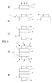
- the invention therefore proposes to reduce the size of the periodic patterns of thickness variation, by providing on at least one side S1, S2 of an assembly to be fractured 5, comprising a support 4 disposed on a surface of a first substrate 1, an absorbent element 6a, 6b suitable for capturing and dissipating the acoustic vibrations emitted during an initiation and/or self-sustained propagation of a fracture wave, as shown in Figure 4 .
- the invention reduces the size of the periodic pattern of thickness variation of the useful layer 3.
- the absorbent element 6a, 6b is suitable for capturing the vibrations emitted in the assembly to be fractured, it may be favourable to limit the reflections of the vibratory waves in the contact zone between the assembly to be fractured 5 and the absorbent element 6a, 6b.
- the absorbent element 6a, 6b can be chosen in such a way that it has an acoustic impedance matched to that of the first substrate 1 and/or the support 4 on which it is disposed. If the first substrate 1 and the support substrate 4 are not of the same type, and in the case where the side S1 of the assembly to be fractured 5 is provided with a first absorbent element 6a, and where the side S2 is provided with a second absorbent element 6b, the first absorbent element 6a will have an acoustic impedance matched to the acoustic impedance of the first substrate 1, and the second absorbent element 6b will have an acoustic impedance matched to the acoustic impedance of the support 4.
- the absorbent element 6a, 6b must preferably be in close contact with the sides S1, S2 of the assembly to be fractured 5 in order to effectively transmit the mechanical deformation of the wafer towards the absorber.
- close contact is understood to mean that the level of contact (i.e. the ratio between the surfaces in contact and the total surface) must be high, for example greater than 70%. Different means can be implemented in order to achieve this close contact. Notably, the following can be mentioned:
- the absorbent element 6a, 6b must also have characteristics ensuring that the captured acoustic vibrations are suitably dissipated.
- a rigid absorbent element will have to be provided with a thickness that is sufficient to dissipate the acoustic vibrations, the absorption then taking place in the thickness of the absorbent element.
- the absorbent element 6a, 6b may be chosen to have visco-elastic properties and to have a high loss factor, greater than 0.01. The energy of the acoustic vibrations is then effectively dissipated through viscous friction.
- This may involve, for example, polyurethane foam (40% density), silicon polymers or composite materials such as a polymer matrix containing high-density dispersed particles, or a composite material formed from a successive stacking of layers of visco-elastic materials and rigid materials (known by the name of "configuration sandwich” or “constrained layer damping").
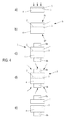
- a strip 7 of material representing material forming the assembly to be fractured having a width of several cm and a length of around 10 cm, is held, for example, on its ends on two supports 8a and 8b.
- This strip is provided, on a first end, with a piezoelectric element 9 connected to an electric generator 10, capable of applying an acoustic vibration with the determined characteristics to the strip 7.
- the strip is also provided, on its other end, with a piezoelectric sensor 11 capable of measuring the characteristics of the propagated acoustic vibrations.
- the main surface of the strip can accommodate an absorbent element to be evaluated 12.
- the absorption and dissipation characteristics of the absorbent element to be evaluated 12 can therefore easily be determined.
- a signal having a controlled shape, frequency and amplitude is applied by means of the electric generator 10, generating an acoustic wave in the strip 7 provided with the absorbent element to be evaluated 12.
- a signal representing the acoustic wave that has propagated in the strip 7 is recorded in the sensor 11.
- the coefficient of absorption of the absorbent element to be evaluated 12 defined as the ratio of the amplitude of the measured signal to the amplitude of the applied signal, can then be represented, according to the frequency.
- the acoustic vibrations which develop in the assembly to be fractured 5 have a main frequency, depending on the implemented layer transfer method parameters (type and dose of the implanted species, temperature and duration of the thermal fragilization treatment, fracture initiation method, etc.).
- the absorbent element must obviously be chosen in order to capture and dissipate the acoustic waves at this main frequency.
- the absorbent element 6a, 6b is preferably positioned on each of the exposed to sides S1, S2 of the assembly to be fractured and the contact zone extends over the entire extent of each of these sides. A maximum absorption of the emitted acoustic vibrations is thus ensured.
- the absorbent element 6a, 6b on a single exposed side S1, S2 of the assembly to be fractured 5.
- the first substrate 1 could then be finally provided with the absorbent element 6a.
- the contact zone may extend over only a part of the extent of the exposed side(s) S1, S2 of the assembly to be fractured 5. This may be advantageous for simplifying the removal of the absorbent element 6a, 6b at the end of the method.
- the contact zone may have a main dimension (length, or diameter according to the shape) at least equal to the order of magnitude of the wavelength of the periodic pattern of thickness variation of the useful layer 3, for example between 1 mm and 100 mm or more. It may thus be decided to position this contact zone facing the fracture wave initiation zone. The acoustic vibrations are then captured and absorbed when they are emitted.
- the initiation zone corresponds to the point of impact of this force on the assembly to be fractured 5.
- the initiation of the fracture is spontaneous, the latter is generally positioned in a particular zone of the assembly to be fractured 5 which can be determined in advance through experimentation and according to the conditions of implementation under which the layer transfer method is carried out.
- the contact zone between the absorbent element 6a, 6b and the exposed surfaces S1, S2 of the element to be fractured 5 can be positioned at the periphery of the assembly to be fractured 5, in such a way as to capture the acoustic vibrations when they are reflected at the ends of the assembly to be fractured 5.
- a fragilization plane is formed through implantation of light species into the first substrate 1.
- the first substrate 1 may be made from silicon, or any other material, semiconducting or otherwise. This may involve, for example, germanium, gallium nitride, lithium tantalate or sapphire. Layers may have been disposed on the surface through deposition or through thermal treatment. This may involve a layer of silicon dioxide, obtained through thermal oxidation of a silicon wafer or through epitaxial deposition of any type: SiGe, InGaN; AlGaN, Ge, etc.
- these may be any species suitable for fragilizing the first substrate 1 in its fragilization plane. This may notably involve hydrogen and/or helium species.
- the fragilization plane along with a surface of the first substrate, delimits the useful layer 3.
- a support 4 is then applied onto the surface of the first substrate 1 in order to form the assembly to be fractured 5.
- the support may consist of a silicon wafer, or a substrate made from any other material of any shape, such as sapphire or glass.
- the support 4 may have been provided with surface layers of any type.
- the application of the support to the surface of the first substrate can be implemented by any direct assembly method: through molecular adhesion, through thermocompression, through electrostatic adhesion, etc.
- the application of the support 4 may also correspond to the deposition of a material onto the surface of the first substrate 1, the deposited layer forming the support 4.
- the absorbent element(s) 6a, 6b is/are then disposed in close contact with the exposed side S1, S2 of the assembly to be fractured 5.
- the absorbent element 6a, 6b may be provided with an adhesive or non-adhesive film (not shown in Figure 4 ) in order to reinforce the close contact.
- the close contact may also be reinforced by establishing the contact in an environment with a pressure lower than atmospheric pressure, in a partial vacuum.
- the appearance of air bubbles at the interface between the exposed surface S1, S2 of the assembly to be fractured 5 and the absorbent element 6a, 6b is thus limited.
- a thermal fragilization treatment is then applied to the assembly to be fractured 5, provided with one or more absorbent elements 6a, 6b.
- this thermal treatment fragilizes the first substrate 1 in its fragilization plane 2, and supplies enough energy for the fracture wave, once initiated, to propagate in a self-sustained manner.
- This thermal treatment is typically between 150°C and 600°C for a period from 30 minutes to 8 hours, such as, for example, for 4 hours at 400°C.
- the thermal treatment is sufficient on its own to initiate the fracture wave.
- the useful layer 3 is entirely detached from the first substrate 1.
- an external force is exerted, during or after the thermal treatment, in order to initiate the fracture wave.
- This external force may be of mechanical origin or of any other origin. It may, for example, be a localized heating implemented by a laser, or a provision of energy through ultrasound.
- a pressure may optionally be exerted on the assembly to be fractured 5 and the absorbent element 6a, 6b, in such a way as to increase their contact surfaces and place this assembly in a close-contact condition.
- This pressure may be exerted via equipment in which the assembly is placed.
- the fracture wave once initiated, propagates in a self-sustained manner in order to detach and transfer the useful layer 2 onto the support 4, as shown in step b) in Figure 4 .
- the acoustic vibrations emitted during the initiation and/or propagation of the fracture wave are captured and absorbed by the absorbent element 6a, 6b. Consequently, the interaction of these acoustic vibrations with the fracture wave is limited and the useful layer has a periodic pattern of thickness variation that is reduced in size.
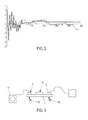
- Figure 2 shows, as a dotted line, a thickness variation profile (in angstroms) along a diameter of a silicon-on-insulator wafer with a diameter of 300 mm obtained through application of the invention, the absorbent element 6a, 6b consisting of a polyurethane foam with a thickness of 3 mm and attached via a PVDC film.
- the size of the thickness variations is less than 0.1 nm.
- This profile can be compared with the continuous-line profile in the same Figure 2 , in which the thickness variations obtained under the same conditions, but without the application of an absorbent element 6a, 6b, were more than 0.3 nm.
- a final step f) (not shown) of the method, the absorbent element 6a, 6b and, in particular, the absorbent element positioned on the side S2 of the support 4 is removed.
- any finishing step (thermal smoothing treatment, thinning through sacrificial oxidation or through etching, etc.) enabling the manufacture of the final structure to be completed can be applied.
- the absorbent element(s) 6a, 6b is/are placed in close contact with the respective exposed sides S1, S2 of the first substrate 1 and/or the support 4, before step b) of application of the support 4 to the surface of the first substrate 1.
- the absorbent elements 6a, 6b are placed in close contact with the exposed sides S1, S2 of the element to be fractured, after step d) of thermal fragilization treatment and before the fracture wave initiation and propagation step.
- the initiation of the fracture wave is caused, after the thermal treatment and once the absorbent element 6a, 6b is positioned, by the application of an external force, for example by the application of a blade L in the fragilization plane 2.
- This third embodiment has the advantage of not exposing the absorbent elements 6a, 6b to the thermal fragilization treatment, which could result in the opposite case in degrading them or rendering their removal more difficult at the end of the method.
- the invention can be applied in particular to the manufacture of a structure comprising a useful layer 3 with a thickness, after finishing, of less than 50 nm or 10 nm.
- a thickness after finishing, of less than 50 nm or 10 nm.
- the contribution of the thickness variations linked to the periodic profile examined by the invention is significant.
- the invention is also particularly useful when the first substrate 1, from which the useful layer 3 originates, has a substantial dimension (200 mm, 300 mm, 450 mm), for which the fracture wave propagation and acoustic vibration effects are more marked.
- the invention may also relate to the manufacture of a silicon-on-insulator wafer, the first substrate 1 then being formed from an oxidized silicon wafer, this support 4 being formed from a silicon wafer.
- the absorbent element 6a, 6b is formed from a very thick silicon wafer (1 cm) provided on one of its sides with a 20-micron (non-adhesive) elastomer film with a Young's modulus of less than 5 GPa.
- An absorbent element 6a, 6b of this type is associated, on the elastomer film side, on each of the exposed sides S1, S2 of the element to be fractured 5, the latter having already undergone the thermal fragilization treatment.
- a pressure exerted on the exposed surfaces of the assembly provides the close contact between the absorbent element 6a, 6b and the assembly to be fractured 5.
- the matching of the acoustic impedances between the elements to be fractured 5 and the absorbent elements 6a, 6b is ensured since they are formed from the same material and the elastomer layer is sufficiently thin to be acoustically transparent.
- the emitted acoustic vibrations are dissipated in the mass of the absorbent elements 6a, 6b.
- An external force such as the insertion of a blade into the fragilization plane, initiates the fracture wave and its self-sustained propagation. Following the removal of the pressure maintaining the close contact of the absorbent elements 6a, 6b, the latter are removed without difficulty, the structure not having undergone any temperature treatment.
- the thick and bare silicon wafers i.e. without the elastomer film of the preceding example, are prepared in advance to have a surface with a roughness of less than 0.5 nm. They are then assembled through molecular adhesion to the first silicon substrate and to the silicon support 4 before the step of application of the support 4 onto the surface of the first substrate 1.
- the method continues, and in the context of this example, the initiation of the fracture wave is obtained during the thermal treatment step which consists in the application of a temperature of 500°C for 1 hour.
- the absorbent elements 6a, 6b are removed from the exposed sides S1, S2 of the first substrate 1 and the support 4 through the introduction of a blade in the adhesion interfaces.
- the absorbent elements 6a, 6b are exposed to the thermal fragilization treatment. This is made possible since no film likely to undergo temperature degradation has been used to establish the close contact.
- the absorbent element 6a, 6b is formed from a PVDC film onto which a layer of around 3 mm of polyurethane foam (having a density of 40%) is electrostatically adhered.
- the absorbent element 6a, 6b has the same dimensions as the first substrate 1 and the support 4.
- At least one absorbent element is electrostatically attached to at least one of the exposed sides S1, S2 of the assembly to be fractured 5, according to the same sequence as in the first example.
- the PVDC film ensures the close contact between the absorbent element 6a, 6b and the first substrate 1 and the support 4 respectively.
- the bond strength nevertheless remains low so that, following the fracture step, it is easy to remove the absorbent elements 6a, 6b.
- the polyurethane foam having a high loss factor greater than 0.01, is particularly suitable for dissipating the captured acoustic vibrations.
- a relatively low thickness, of a few mm, is enough to significantly reduce the size of the periodic profile of thickness variation of the useful layer 3.
- the absorbent element 6a, 6b is formed from a sandwich configuration comprising, for example, a stack of 10 to 20 successive layers including, in a repeated manner, a first adhesive polymer film with a thickness of around 100 microns and an aluminium metal sheet also of around 100 microns.
- the stack has a total thickness of between 1 and 5 mm.
- This absorbent element 6a, 6b is positioned in close contact with the exposed sides S1, S2 of the assembly to be fractured 5, via the surface polymer layer of the absorbent element 6a, 6b.
- This absorbent element 6a, 6b has a high loss factor, well above 0.01, the acoustic vibration in fact causing a shearing of the polymer layers, caused by the relatively rigid aluminium sheets.
- This particular configuration of the absorbent element 6a, 6b results in a particularly effective dissipation of the transmitted acoustic power. Consequently, the size of the periodic pattern of thickness vibration of the useful layer is particularly reduced.
Landscapes
- Transducers For Ultrasonic Waves (AREA)
- Surface Acoustic Wave Elements And Circuit Networks Thereof (AREA)
Abstract
- formation of a fragilization plane (2) through the implantation of light species into a first substrate (1) in such a way as to form a useful layer (3) between this plane and a surface of the first substrate (1);
- application of the support (4) onto the surface of the first substrate (1) to form an assembly to be fractured (5) having two exposed sides (S1, S2);
- thermal fragilization treatment of the assembly to be fractured (5);
- initiation and self-sustained propagation of a fracture wave in the first substrate (1) along the fragilization plane (2).
Description
- The present invention relates to a method for transferring a useful layer onto a supporting substrate.
- A method for transferring a
useful layer 3 onto a supportingsubstrate 4, shown inFigure 1 , is known from the prior art, this method including the following main steps: - in a step a), the formation of a
fragilization plane 2 through the implantation of light species into afirst substrate 1 in such a way as to form auseful layer 3 between this plane and a surface of the first substrate; - in a step b), the application of the
support 4 onto the surface of thefirst substrate 1 to form an assembly to be fractured 5, having two exposed sides S1, S2; - in a step c), the thermal fragilization treatment of the assembly to be fractured 5;
- in a step d), the initiation and self-sustained propagation of a fracture wave in the
first substrate 1 along thefragilization plane 2. - During this method, the implanted species cause the development of microcavities. The effect of the thermal fragilization treatment is to promote the coalescence and pressurization of these microcavities. Under the effect of this thermal treatment alone, or through additional external forces, the initiation and self-sustained propagation of a fracture wave enables the transfer of the
useful layer 3 through detachment in thefragilization plane 2. - This method, described notably in the documents
WO2005043615 andWO2005043616 and designated by the name of "Smart Cut™", is useful in particular for the manufacture of silicon-on-insulator substrates. In this case, thefirst substrate 1 and thesupport 4 are formed from a silicon wafer, and one or the other of thefirst substrate 1 and thesupport 4 are surface-oxidized. - These silicon-on-insulator substrates must comply with very precise specifications. This applies in particular to the average thickness and uniformity of thickness of the
useful layer 3. Compliance with these specifications is required for the correct operation of the semiconductor devices that will be formed in or on thisuseful layer 3. - In some cases, the architecture of these semiconductor devices requires the provision of silicon-on-insulator substrates having a very low average thickness of the
useful layer 3, for example less than 50 nm, or even less than 10 nm, and a uniformity of thickness that is highly constant on the surface of the substrate (the normalized diameter of which is typically 200 mm, 300 mm, and even 450 mm for the next generations). The expected uniformity of thickness may thus be in the order of at most 1%, corresponding to variation maxima typically ranging from +/0.1 nm to +/-1 nm over the entire surface of the wafer. - It is customary, in terms of the "Smart Cut" method, to apply complementary steps of finishing of the
useful layer 3, such as etchings or surface-smoothing thermal treatments in order to seek to achieve the expected specification level. - The applicants in the case of the present invention have observed the presence, following the fracture step, of variations in the thickness of the
useful layer 3 with a quite specific profile. These variations in thickness in fact appear in the form of a periodic pattern, the size of which is in the order of a nanometre, or even a half-nanometre, and the wavelength of which is in order of a millimetre, or even a centimetre. The periodic pattern may be apparent over the entire useful layer, or over a part only. This periodic pattern is thus visible on the thickness variation profile (in angstroms) along a diameter of a useful layer of a silicon-on-insulator wafer with a diameter of 300 mm obtained according to the Smart Cut™ method of the prior art shown inFigure 2 by a continuous line. - It is particularly difficult to correct this particular thickness non-uniformity profile using customary finishing techniques (etching, sacrificial oxidation, thermal softening treatment) as these techniques are ineffective in the wavelength range which these patterns have. Consequently, this periodic pattern contributes to the thickness non-uniformity of the
useful layer 3 following the application of the finishing steps, which does not allow the required uniformity level to be achieved when the latter is significant. - One object of the invention is to propose a method for transferring a useful layer onto a support substrate, this useful layer having a periodic pattern of thickness variation, the size of which is reduced.
- Studies carried out by the applicants in connection with the present invention have produced the finding that the origin of this periodic pattern lay in the interaction between the fracture wave and acoustic vibrations encountered in the assembly to be fractured.
- More precisely, the inventors of the present application found that the initiation and/or propagation of the fracture wave was liable to cause this assembly to vibrate. These Lamb-wave vibrations propagate without significant attenuation over distances comparable to the size of the substrates, and at a speed greater than the speed of the self-sustained fracture wave. They are reflected, once or several times, on the ends of the assembly to be fractured, which helps to maintain this acoustic vibration in the assembly during the propagation of the fracture wave. In relation to the present invention, the inventors have thus found that the modulation of the fracture wave by these acoustic vibrations was the cause of the periodic pattern of thickness variation observed on the useful layer at the end of the method.
- With a view to achieving the aforementioned object, the subject-matter of the invention proposes a method for transferring a useful layer onto a support including the following steps of:
- formation of a fragilization plane through implantation of light species into a first substrate in such a way as to form a useful layer between this plane and a surface of the first substrate;
- application of a support onto the surface of the first substrate to form an assembly to be fractured, having two exposed sides;
- thermal fragilization treatment of the assembly to be fractured;
- initiation and self-sustained propagation of a fracture wave in the first substrate along the fragilization plane.
- According to the invention, at least one of the sides of the assembly to be fractured is in close contact, over a contact zone, with an absorbent element suitable for capturing and dissipating the acoustic vibrations emitted during the initiation and/or propagation of the fracture wave.
- Since at least some of the emitted acoustic vibrations are absorbed by the absorbent element, the interaction of these acoustic vibrations with the fracture wave is less, and the useful layer has a periodic pattern of thickness variation that is reduced in size.
- According to other advantageous and non-limiting characteristics of the invention, taken alone or in combination:
- the acoustic vibrations have a main frequency, and the absorbent element is chosen to capture and dissipate the acoustic waves at this main frequency;
- the contact zone extends over a part of the extent of the side of the assembly to be fractured;
- the contact zone is positioned on the side of the assembly to be fractured facing the fracture wave initiation zone;
- the initiation of the fracture wave is obtained during the thermal fragilization treatment step;
- the initiation of the fracture wave is obtained through application of a mechanical force in the fragilization plane;
- the absorbent element is placed in close contact with the side of the assembly to be fractured after the thermal treatment step and before the fracture wave initiation step through application of a mechanical force;
- a first and a second absorbent element are disposed on each of the sides of the assembly to be fractured;
- the close contact between the side of the assembly to be fractured and the absorbent element is obtained by way of a film disposed between the assembly to be fractured and the absorbent element;
- the film is formed from an adhesive material;
- the film is formed from a non-adhesive material, with a low Young's modulus of less than 5 GPa;
- the close contact between the side of the assembly to be fractured and the absorbent element is obtained through application of a pressure onto the absorbent element;
- the side of the assembly to be fractured and the absorbent element have a surface roughness of less than 0.5 nm, the close contact between the side of the assembly to be fractured and the absorbent element being obtained through their direct assembly;
- the absorbent element is made from a material having a high loss factor, greater than 0.01;
- the absorbent element has a thickness greater than 1 mm.
- The invention will be better understood in the light of the description which follows of particular non-limiting embodiments of the invention with reference to the attached figures, in which:
-
Figure 1 shows a method for transferring a useful layer onto a support according to the prior art; -
Figure 2 shows a thickness variation profile (in angstroms) of a silicon-on-insulator wafer with a diameter of 300 mm, for the method according to the prior art (continuous line) and according to the invention (dotted line); -
Figure 3 shows a characterization test bench for an absorbent element to be evaluated; -
Figure 4 shows a first embodiment of the invention; -
Figure 5 shows a second embodiment of the invention; -
Figure 6 shows a third embodiment of the invention. - In order to simplify the description that follows, the same references are used for elements that are identical or perform the same function in the different described embodiments of the method, or in the method according to the prior art.
- As mentioned, the studies carried out by the applicants in connection with the present invention have produced the finding that the origin of the periodic pattern of thickness variation of a
useful layer 3 transferred by the Smart Cut method of the prior art lay in the interaction between the self-sustained propagation of the fracture wave and the acoustic vibrations encountered in the assembly to be fractured. The fracture wave is in fact deviated vertically from its plane of progression according to the state of instantaneous constraint of the material through which it passes. - The term "self-sustained fracture wave" is understood to mean that the fracture, once initiated in an initiation zone, propagates autonomously, without the application of additional external force, and over the entire extent of the fragilization plane, in such a way as to detach completely the useful layer from the
first substrate 1. - During the thermal fragilization treatment, energy is absorbed in the fragilization plane, for example in the form of pressure within the microcavities which develop there. On initiation of the fracture, the energy is released, causing the fracture front to progress spontaneously, resulting in the formation of a self-sustained fracture wave.
- The inventors of the present application have thus found that, by equipping the assembly to be fractured 5 with piezoelectric sensors, the acoustic vibrations assumed the form of Lamb waves. A Lamb wave is a mechanical wave propagating, almost without attenuation, in a thin wafer of material, guided by the surfaces of the wafer.
- The inventors also observed during their experimentation that the characteristic quantities of these waves were determined by the parameters of obtaining the fracture wave. Thus, and by way of example, when the layer transfer method of the prior art is obtained through:
- implementation of hydrogen species, with a dose of 5x10¹⁶ species/cm2 in a
first substrate 1 formed from an oxidized silicon wafer; - application of a
support 4 formed from a silicon wafer; - thermal fragilization treatment carried out at 400°C for 4 hours, during which the fracture wave is initiated spontaneously.
- The measured acoustic vibrations are mainly A0-mode Lamb waves with a main frequency of 2 MHz.
- When, in a second example, the thermal fragilization treatment is replaced by an annealing at 350°C for 2 hours and the initiation of the fracture wave caused by the application of an external mechanical force in an initiation zone, the measured acoustic vibrations are mainly A0-mode Lamb waves with a main frequency of 100 kHz.
- In any event, the studies carried out during the development of the present invention on the method of the prior art established that acoustic variations are emitted during the initiation and/or self-sustained propagation of the fracture wave in the assembly to be fractured 5, and that these acoustic vibrations were the cause of the periodic pattern of thickness variation of the
useful layer 3. - The invention therefore proposes to reduce the size of the periodic patterns of thickness variation, by providing on at least one side S1, S2 of an assembly to be fractured 5, comprising a
support 4 disposed on a surface of afirst substrate 1, anabsorbent element Figure 4 . - Thus, by limiting the development of the acoustic vibrations in the assembly to be fractured 5, the invention reduces the size of the periodic pattern of thickness variation of the
useful layer 3. - In a very general manner, the use of an absorbent element to attenuate the development of vibrations is very widespread. Moreover, numerous forms and types of this element are likely to be suitable in the application comprising the subject-matter of the present invention.
- So that the
absorbent element absorbent element - In order to achieve this object, the
absorbent element first substrate 1 and/or thesupport 4 on which it is disposed. If thefirst substrate 1 and thesupport substrate 4 are not of the same type, and in the case where the side S1 of the assembly to be fractured 5 is provided with a firstabsorbent element 6a, and where the side S2 is provided with a secondabsorbent element 6b, the firstabsorbent element 6a will have an acoustic impedance matched to the acoustic impedance of thefirst substrate 1, and the secondabsorbent element 6b will have an acoustic impedance matched to the acoustic impedance of thesupport 4. - Furthermore, the
absorbent element - the use of an adhesive film, for example a polymer adhesive, between the absorbent element and the assembly to be fractured 5;
- the use of a non-adhesive film with a low Young's modulus of less than 5 GPa, such as, for example, an elastomer, between the absorbent element and the assembly to be fractured 5. In this case, the close contact may be achieved by submitting the assembly to compression forces;
- the use of an electrostatically adhesive film between the
absorbent element - the assembly of the
absorbent element - the deposition on the contact zone of a layer of materials, this layer then forming the
absorbent element - Moreover, the
absorbent element - Generally speaking, a rigid absorbent element will have to be provided with a thickness that is sufficient to dissipate the acoustic vibrations, the absorption then taking place in the thickness of the absorbent element.
- Alternatively, the
absorbent element - The choice of the suitable absorbent element may be determined through a limited number of tests on a test bench that is simple to implement, as shown in
Figure 3 . In this figure, astrip 7 of material representing material forming the assembly to be fractured, having a width of several cm and a length of around 10 cm, is held, for example, on its ends on twosupports piezoelectric element 9 connected to anelectric generator 10, capable of applying an acoustic vibration with the determined characteristics to thestrip 7. The strip is also provided, on its other end, with apiezoelectric sensor 11 capable of measuring the characteristics of the propagated acoustic vibrations. The main surface of the strip can accommodate an absorbent element to be evaluated 12. - The absorption and dissipation characteristics of the absorbent element to be evaluated 12 can therefore easily be determined. A signal having a controlled shape, frequency and amplitude is applied by means of the
electric generator 10, generating an acoustic wave in thestrip 7 provided with the absorbent element to be evaluated 12. A signal representing the acoustic wave that has propagated in thestrip 7 is recorded in thesensor 11. The coefficient of absorption of the absorbent element to be evaluated 12, defined as the ratio of the amplitude of the measured signal to the amplitude of the applied signal, can then be represented, according to the frequency. - Using this test bench, it is very simple to determine the absorption and dissipation characteristics of an absorbent element to be evaluated 12.
- In particular, and as previously seen, the acoustic vibrations which develop in the assembly to be fractured 5 have a main frequency, depending on the implemented layer transfer method parameters (type and dose of the implanted species, temperature and duration of the thermal fragilization treatment, fracture initiation method, etc.). The absorbent element must obviously be chosen in order to capture and dissipate the acoustic waves at this main frequency.
- The
absorbent element - However, in order to simplify the method according to the invention, it is also possible to position the
absorbent element first substrate 1 which, generally, following the transfer of theuseful layer 3, is reprocessed and reused as the first substrate in a new layer transfer method. Thefirst substrate 1 could then be finally provided with theabsorbent element 6a. - Regardless of whether the
absorbent element absorbent element useful layer 3, for example between 1 mm and 100 mm or more. It may thus be decided to position this contact zone facing the fracture wave initiation zone. The acoustic vibrations are then captured and absorbed when they are emitted. In the case where the initiation is caused by the application of an external force, the initiation zone corresponds to the point of impact of this force on the assembly to be fractured 5. When the initiation of the fracture is spontaneous, the latter is generally positioned in a particular zone of the assembly to be fractured 5 which can be determined in advance through experimentation and according to the conditions of implementation under which the layer transfer method is carried out. - Alternatively, the contact zone between the
absorbent element - Once the characteristics of the
absorbent element Figures 4 to 6 . - In a first step a), shown in
Figure 4 , a fragilization plane is formed through implantation of light species into thefirst substrate 1. Thefirst substrate 1 may be made from silicon, or any other material, semiconducting or otherwise. This may involve, for example, germanium, gallium nitride, lithium tantalate or sapphire. Layers may have been disposed on the surface through deposition or through thermal treatment. This may involve a layer of silicon dioxide, obtained through thermal oxidation of a silicon wafer or through epitaxial deposition of any type: SiGe, InGaN; AlGaN, Ge, etc. - As far as the light species are concerned, these may be any species suitable for fragilizing the
first substrate 1 in its fragilization plane. This may notably involve hydrogen and/or helium species. - The fragilization plane, along with a surface of the first substrate, delimits the
useful layer 3. - In a second step b), a
support 4 is then applied onto the surface of thefirst substrate 1 in order to form the assembly to be fractured 5. The support may consist of a silicon wafer, or a substrate made from any other material of any shape, such as sapphire or glass. As with thefirst substrate 1, thesupport 4 may have been provided with surface layers of any type. - The application of the support to the surface of the first substrate can be implemented by any direct assembly method: through molecular adhesion, through thermocompression, through electrostatic adhesion, etc. The application of the
support 4 may also correspond to the deposition of a material onto the surface of thefirst substrate 1, the deposited layer forming thesupport 4. - In a following step c) and according to a first embodiment of the invention, the absorbent element(s) 6a, 6b is/are then disposed in close contact with the exposed side S1, S2 of the assembly to be fractured 5. As previously described, the
absorbent element Figure 4 ) in order to reinforce the close contact. - The close contact may also be reinforced by establishing the contact in an environment with a pressure lower than atmospheric pressure, in a partial vacuum. The appearance of air bubbles at the interface between the exposed surface S1, S2 of the assembly to be fractured 5 and the
absorbent element - In a following step d), a thermal fragilization treatment is then applied to the assembly to be fractured 5, provided with one or more
absorbent elements first substrate 1 in itsfragilization plane 2, and supplies enough energy for the fracture wave, once initiated, to propagate in a self-sustained manner. This thermal treatment is typically between 150°C and 600°C for a period from 30 minutes to 8 hours, such as, for example, for 4 hours at 400°C. - In a first alternative embodiment, the thermal treatment is sufficient on its own to initiate the fracture wave. At the end of the thermal treatment, the
useful layer 3 is entirely detached from thefirst substrate 1. - In a second alternative embodiment, an external force is exerted, during or after the thermal treatment, in order to initiate the fracture wave. This external force may be of mechanical origin or of any other origin. It may, for example, be a localized heating implemented by a laser, or a provision of energy through ultrasound.
- During the application of the thermal treatment, a pressure may optionally be exerted on the assembly to be fractured 5 and the
absorbent element - Regardless of the alternative embodiment that is implemented, the fracture wave, once initiated, propagates in a self-sustained manner in order to detach and transfer the
useful layer 2 onto thesupport 4, as shown in step b) inFigure 4 . - According to the invention, the acoustic vibrations emitted during the initiation and/or propagation of the fracture wave are captured and absorbed by the
absorbent element - In this respect,
Figure 2 shows, as a dotted line, a thickness variation profile (in angstroms) along a diameter of a silicon-on-insulator wafer with a diameter of 300 mm obtained through application of the invention, theabsorbent element Figure 2 , in which the thickness variations obtained under the same conditions, but without the application of anabsorbent element - In a final step f) (not shown) of the method, the
absorbent element support 4 is removed. - Before, or preferably after, this removal step, any finishing step (thermal smoothing treatment, thinning through sacrificial oxidation or through etching, etc.) enabling the manufacture of the final structure to be completed can be applied.
- In a second embodiment of the structure, shown in
Figure 5 , the absorbent element(s) 6a, 6b is/are placed in close contact with the respective exposed sides S1, S2 of thefirst substrate 1 and/or thesupport 4, before step b) of application of thesupport 4 to the surface of thefirst substrate 1. - According to a third, and particularly advantageous, embodiment, shown in
Figure 6 , theabsorbent elements - In this case, the initiation of the fracture wave is caused, after the thermal treatment and once the
absorbent element fragilization plane 2. - This third embodiment has the advantage of not exposing the
absorbent elements - By limiting the size of the periodic pattern of thickness variation of the
useful layer 3, the invention can be applied in particular to the manufacture of a structure comprising auseful layer 3 with a thickness, after finishing, of less than 50 nm or 10 nm. In fact, for this thickness, the contribution of the thickness variations linked to the periodic profile examined by the invention (in the order of a nanometre) is significant. The invention is also particularly useful when thefirst substrate 1, from which theuseful layer 3 originates, has a substantial dimension (200 mm, 300 mm, 450 mm), for which the fracture wave propagation and acoustic vibration effects are more marked. - The invention may also relate to the manufacture of a silicon-on-insulator wafer, the
first substrate 1 then being formed from an oxidized silicon wafer, thissupport 4 being formed from a silicon wafer. - The examples which follow therefore illustrate the invention, applied to the manufacture of a silicon-on-insulator structure of this type.
- In a first example, the
absorbent element absorbent element absorbent element absorbent elements absorbent elements - An external force, such as the insertion of a blade into the fragilization plane, initiates the fracture wave and its self-sustained propagation. Following the removal of the pressure maintaining the close contact of the
absorbent elements - In a second example, the thick and bare silicon wafers, i.e. without the elastomer film of the preceding example, are prepared in advance to have a surface with a roughness of less than 0.5 nm. They are then assembled through molecular adhesion to the first silicon substrate and to the
silicon support 4 before the step of application of thesupport 4 onto the surface of thefirst substrate 1. The method continues, and in the context of this example, the initiation of the fracture wave is obtained during the thermal treatment step which consists in the application of a temperature of 500°C for 1 hour. - Following the fracture, the
absorbent elements first substrate 1 and thesupport 4 through the introduction of a blade in the adhesion interfaces. In this example, theabsorbent elements - In a third example, the
absorbent element absorbent element first substrate 1 and thesupport 4. At least one absorbent element is electrostatically attached to at least one of the exposed sides S1, S2 of the assembly to be fractured 5, according to the same sequence as in the first example. - The PVDC film ensures the close contact between the
absorbent element first substrate 1 and thesupport 4 respectively. The bond strength nevertheless remains low so that, following the fracture step, it is easy to remove theabsorbent elements useful layer 3. - In a final example, the
absorbent element absorbent element absorbent element absorbent element absorbent element - The invention is obviously not limited to the embodiments described, and alternative embodiments can be provided without exceeding the scope of the invention as defined by the claims.
Claims (21)
- Method for transferring a useful layer (3) onto a support (4), including the following main steps:- formation of a fragilization plane (2) through the implantation of light species into a first substrate (1) in such a way as to form a useful layer (3) between this plane and a surface of the first substrate (1);- application of the support (4) onto the surface of the first substrate (1) to form an assembly to be fractured (5), having two exposed sides (S1, S2);- thermal fragilization treatment of the assembly to be fractured (5);- initiation and self-sustained propagation of a fracture wave in the first substrate (1) along the fragilization plane (2);the method being characterized in that at least one of the sides (S1, S2) of the assembly to be fractured (5) is in close contact, over a contact zone, with an absorbent element (6a, 6b) suitable for capturing and dissipating the acoustic vibrations emitted during the initiation and/or propagation of the fracture wave.
- Method according to Claim 1, in which the acoustic vibrations have a main frequency, and the absorbent element (6a, 6b) is chosen to capture and dissipate the acoustic waves at this main frequency.
- Method according to Claims 1 or 2 , in which the contact zone extends over a part of the extent of the side (S1, S2) of the assembly to be fractured.
- Method according to Claim 3, in which the contact zone is positioned on the side (S1, S2) of the assembly to be fractured (5) facing the fracture wave initiation zone.
- Method according to any one of the preceding claims, in which the thermal fragilization treatment is between 150°C and 600°C, for a period from 30 minutes to 8 hours.
- Method according to one of the preceding claims, in which the initiation of the fracture wave is obtained during the thermal fragilization treatment step.
- Method according to one of the preceding claims, in which the initiation of the fracture wave is obtained through application of a mechanical force in the fragilization plane.
- Method according to the preceding claim, in which the absorbent element (6a, 6b) is placed in close contact with the side (S1, S2) of the assembly to be fractured (5) after the thermal treatment step and before the fracture wave initiation step through application of a mechanical force.
- Method according to any one of the preceding claims, in which, after the fracture wave initiation and propagation step, the absorbent element (6a, 6b) is removed.
- Method according to any one of the preceding claims, in which a first and a second absorbent element (6a, 6b) are disposed on each of the sides (S1, S2) of the assembly to be fractured (5).
- Method according to any one of the preceding claims, in which the side (S1) of the assembly to be fractured (5) is in close contact, on the side of the first substrate (1), with the first absorbent element (6a) having an acoustic impedance matched to the acoustic impedance of the first substrate (1).
- Method according to any one of the preceding claims, in which the side (S2) of the assembly to be fractured (5) is in close contact, on the side of the support (4) with the second absorbent element (6b) having an acoustic impedance matched to the acoustic impedance of the support (4).
- Method according to any one of the preceding claims, in which the close contact between the side (S1, S2) of the assembly to be fractured (5) and the absorbent element (6a, 6b) is obtained by way of a film (7a, 7b) disposed between the assembly to be fractured (5) and the absorbent element (6a, 6b).
- Method according to the preceding claim, in which the film (7a, 7b) is formed from an adhesive material.
- Method according to Claim 13, in which the film adheres electrostatically to the side (S1, S2) of the assembly to be fractured (5) and the absorbent element (6a, 6b).
- Method according to Claim 13, in which the film is formed from a non-adhesive material with a low Young's modulus of less than 5 GPa.
- Method according to any one of the preceding claims, in which the close contact between the side (S1, S2) of the assembly to be fractured (5) and the absorbent element (6a, 6b) is obtained through application of a pressure onto the absorbent element (6a, 6b).
- Method according to any one of the preceding claims, in which the side (S1, S2) of the assembly to be fractured (5) and the absorbent element (6a, 6b) have a surface roughness of less than 0.5 nm; the close contact between the side (S1, S2) of the assembly to be fractured (5) and the absorbent element (6a, 6b) is obtained through their direct assembly.
- Method according to any one of the preceding claims, in which the absorbent element (6a, 6b) is made from a material having a high loss factor greater than 0.01.
- Method according to the preceding claim, in which the absorbent element (6a, 6b) is formed from a visco-elastic material or a composite material or a sandwich configuration.
- Method according to any one of the preceding claims, in which the absorbent element (6a, 6b) has a thickness greater than 1 mm.
Applications Claiming Priority (1)
| Application Number | Priority Date | Filing Date | Title |
|---|---|---|---|
| FR1453400A FR3020175B1 (en) | 2014-04-16 | 2014-04-16 | METHOD OF TRANSFERRING A USEFUL LAYER |
Publications (2)
| Publication Number | Publication Date |
|---|---|
| EP2933828A1 true EP2933828A1 (en) | 2015-10-21 |
| EP2933828B1 EP2933828B1 (en) | 2016-10-19 |
Family
ID=51726593
Family Applications (1)
| Application Number | Title | Priority Date | Filing Date |
|---|---|---|---|
| EP15162329.5A Active EP2933828B1 (en) | 2014-04-16 | 2015-04-02 | Method for transferring a useful layer |
Country Status (9)
| Country | Link |
|---|---|
| US (1) | US9589830B2 (en) |
| EP (1) | EP2933828B1 (en) |
| JP (1) | JP6481202B2 (en) |
| KR (1) | KR102333997B1 (en) |
| CN (1) | CN105023876B (en) |
| DK (1) | DK2933828T3 (en) |
| FR (1) | FR3020175B1 (en) |
| SG (1) | SG10201503005RA (en) |
| TW (1) | TWI648765B (en) |
Cited By (5)
| Publication number | Priority date | Publication date | Assignee | Title |
|---|---|---|---|---|
| WO2018029419A1 (en) * | 2016-08-11 | 2018-02-15 | Soitec | Method for transferring a useful layer |
| FR3093860A1 (en) * | 2019-03-15 | 2020-09-18 | Soitec | Method of transferring a useful layer onto a support substrate |
| FR3093859A1 (en) * | 2019-03-15 | 2020-09-18 | Soitec | Method of transferring a useful layer onto a support substrate |
| FR3093858A1 (en) * | 2019-03-15 | 2020-09-18 | Soitec | Method of transferring a useful layer onto a support substrate |
| FR3108440A1 (en) | 2020-03-23 | 2021-09-24 | Soitec | Process for preparing a thin layer |
Families Citing this family (7)
| Publication number | Priority date | Publication date | Assignee | Title |
|---|---|---|---|---|
| JP6563360B2 (en) * | 2016-04-05 | 2019-08-21 | 信越化学工業株式会社 | Method for manufacturing composite wafer having oxide single crystal thin film |
| FR3061988B1 (en) | 2017-01-13 | 2019-11-01 | Soitec | SURFACE MELTING METHOD OF SEMICONDUCTOR SUBSTRATE ON INSULATION |
| US10679908B2 (en) * | 2017-01-23 | 2020-06-09 | Globalwafers Co., Ltd. | Cleave systems, mountable cleave monitoring systems, and methods for separating bonded wafer structures |
| FR3079658B1 (en) * | 2018-03-28 | 2021-12-17 | Soitec Silicon On Insulator | METHOD OF DETECTION OF THE FRACTURE OF A FRAGILIZED SUBSTRATE BY IMPLANTATION OF ATOMIC SPECIES |
| FR3094563A1 (en) * | 2019-03-29 | 2020-10-02 | Soitec | MANUFACTURING PROCESS OF A SEMICONDUCTOR SUBSTRATE ON INSULATION |
| IL293087A (en) * | 2019-11-22 | 2022-07-01 | Exo Imaging Inc | Ultrasound transducer with acoustic absorber structure |
| FR3112240B1 (en) * | 2020-07-06 | 2022-06-03 | Soitec Silicon On Insulator | SEMICONDUCTIVE STRUCTURE COMPRISING AN ELECTRICALLY CONDUCTIVE BONDING INTERFACE, AND METHOD FOR FABRICATING THEREOF |
Citations (2)
| Publication number | Priority date | Publication date | Assignee | Title |
|---|---|---|---|---|
| WO2001080308A2 (en) * | 2000-04-14 | 2001-10-25 | S.O.I.Tec Silicon On Insulator Technologies | Method for cutting out at least a thin layer in a substrate or ingot, in particular made of semiconductor material(s) |
| FR2861497A1 (en) * | 2003-10-28 | 2005-04-29 | Soitec Silicon On Insulator | METHOD FOR CATASTROPHIC TRANSFER OF A FINE LAYER AFTER CO-IMPLANTATION |
Family Cites Families (4)
| Publication number | Priority date | Publication date | Assignee | Title |
|---|---|---|---|---|
| FR2809867B1 (en) * | 2000-05-30 | 2003-10-24 | Commissariat Energie Atomique | FRAGILE SUBSTRATE AND METHOD FOR MANUFACTURING SUCH SUBSTRATE |
| JP4995626B2 (en) * | 2007-04-27 | 2012-08-08 | 信越化学工業株式会社 | Manufacturing method of bonded substrate |
| JP5876646B2 (en) * | 2010-11-02 | 2016-03-02 | キヤノン株式会社 | Electromechanical converter |
| JP5704602B2 (en) * | 2011-03-17 | 2015-04-22 | リンテック株式会社 | Thin semiconductor device manufacturing method and support for brittle member |
-
2014
- 2014-04-16 FR FR1453400A patent/FR3020175B1/en not_active Expired - Fee Related
-
2015
- 2015-04-02 EP EP15162329.5A patent/EP2933828B1/en active Active
- 2015-04-02 DK DK15162329.5T patent/DK2933828T3/en active
- 2015-04-03 JP JP2015076933A patent/JP6481202B2/en active Active
- 2015-04-14 US US14/686,229 patent/US9589830B2/en active Active
- 2015-04-15 TW TW104112125A patent/TWI648765B/en active
- 2015-04-15 CN CN201510177940.2A patent/CN105023876B/en active Active
- 2015-04-16 SG SG10201503005RA patent/SG10201503005RA/en unknown
- 2015-04-16 KR KR1020150054032A patent/KR102333997B1/en active Active
Patent Citations (4)
| Publication number | Priority date | Publication date | Assignee | Title |
|---|---|---|---|---|
| WO2001080308A2 (en) * | 2000-04-14 | 2001-10-25 | S.O.I.Tec Silicon On Insulator Technologies | Method for cutting out at least a thin layer in a substrate or ingot, in particular made of semiconductor material(s) |
| FR2861497A1 (en) * | 2003-10-28 | 2005-04-29 | Soitec Silicon On Insulator | METHOD FOR CATASTROPHIC TRANSFER OF A FINE LAYER AFTER CO-IMPLANTATION |
| WO2005043616A1 (en) | 2003-10-28 | 2005-05-12 | S.O.I. Tec Silicon On Insulator Technologies | Method for the catastrophic transfer of a thin layer after co-implantation |
| WO2005043615A1 (en) | 2003-10-28 | 2005-05-12 | S.O.I.Tec Silicon On Insulator Technologies | Method for self- supported transfer of a fine layer by pulsation after implantation or co-implantation |
Cited By (16)
| Publication number | Priority date | Publication date | Assignee | Title |
|---|---|---|---|---|
| WO2018029419A1 (en) * | 2016-08-11 | 2018-02-15 | Soitec | Method for transferring a useful layer |
| FR3055063A1 (en) * | 2016-08-11 | 2018-02-16 | Soitec Silicon On Insulator | METHOD OF TRANSFERRING A USEFUL LAYER |
| TWI738834B (en) * | 2016-08-11 | 2021-09-11 | 法商索泰克公司 | A method for transferring a useful layer |
| FR3093858A1 (en) * | 2019-03-15 | 2020-09-18 | Soitec | Method of transferring a useful layer onto a support substrate |
| FR3093859A1 (en) * | 2019-03-15 | 2020-09-18 | Soitec | Method of transferring a useful layer onto a support substrate |
| WO2020188169A1 (en) * | 2019-03-15 | 2020-09-24 | Soitec | Method for transferring a useful layer to a carrier substrate |
| WO2020188168A1 (en) | 2019-03-15 | 2020-09-24 | Soitec | Method for transferring a useful layer onto a support substrate |
| WO2020188167A1 (en) | 2019-03-15 | 2020-09-24 | Soitec | Method for transferring a useful layer onto a support substrate |
| FR3093860A1 (en) * | 2019-03-15 | 2020-09-18 | Soitec | Method of transferring a useful layer onto a support substrate |
| CN113491005A (en) * | 2019-03-15 | 2021-10-08 | 索泰克公司 | Method for transferring a useful layer to a carrier substrate |
| KR20210134784A (en) * | 2019-03-15 | 2021-11-10 | 소이텍 | The process of transferring the useful layer to the carrier substrate |
| TWI811528B (en) * | 2019-03-15 | 2023-08-11 | 法商索泰克公司 | Process for transferring a useful layer to a carrier substrate |
| TWI851665B (en) * | 2019-03-15 | 2024-08-11 | 法商索泰克公司 | Process for transferring a useful layer to a carrier substrate |
| CN113491005B (en) * | 2019-03-15 | 2025-07-08 | 索泰克公司 | Method for transferring a useful layer to a carrier substrate |
| FR3108440A1 (en) | 2020-03-23 | 2021-09-24 | Soitec | Process for preparing a thin layer |
| WO2021191513A1 (en) | 2020-03-23 | 2021-09-30 | Soitec | Method for preparing a thin layer |
Also Published As
| Publication number | Publication date |
|---|---|
| KR102333997B1 (en) | 2021-12-02 |
| DK2933828T3 (en) | 2017-01-23 |
| FR3020175A1 (en) | 2015-10-23 |
| CN105023876A (en) | 2015-11-04 |
| JP2015213161A (en) | 2015-11-26 |
| US20150303098A1 (en) | 2015-10-22 |
| TW201611085A (en) | 2016-03-16 |
| KR20150119822A (en) | 2015-10-26 |
| TWI648765B (en) | 2019-01-21 |
| CN105023876B (en) | 2019-05-17 |
| FR3020175B1 (en) | 2016-05-13 |
| SG10201503005RA (en) | 2015-11-27 |
| US9589830B2 (en) | 2017-03-07 |
| JP6481202B2 (en) | 2019-03-13 |
| EP2933828B1 (en) | 2016-10-19 |
Similar Documents
| Publication | Publication Date | Title |
|---|---|---|
| EP2933828B1 (en) | Method for transferring a useful layer | |
| TWI718279B (en) | Manufacturing method of composite wafer with oxide single crystal film | |
| US8951886B2 (en) | Method for separating a layer system comprising a wafer by precisely maintaining the position of the separating front | |
| US9847243B2 (en) | Debonding a glass substrate from carrier using ultrasonic wave | |
| JP2012513684A5 (en) | ||
| KR20180014700A (en) | METHOD FOR MANUFACTURING COMPOSITE WAFER WITH OXIDE SINGLE CRYSTAL FILM | |
| US9427948B2 (en) | Manufacturing a flexible structure by transfers of layers | |
| KR20180014701A (en) | METHOD FOR MANUFACTURING COMPOSITE WAFER WITH OXIDE SINGLE CRYSTAL FILM | |
| CN105027436A (en) | Composite substrate, elastic wave device and method for manufacturing elastic wave device | |
| JP7668864B2 (en) | Hybrid Construction | |
| JP2011071518A (en) | Method for ultrasonic planarization of substrate, from surface whose buried weakened layer has been exposed by fracture | |
| US10950491B2 (en) | Method for transferring a useful layer | |
| CN113574654B (en) | Method for transferring a useful layer to a carrier substrate | |
| HK1165092A (en) | Method for separating a layer system comprising a wafer | |
| HK1165092B (en) | Method for separating a layer system comprising a wafer |
Legal Events
| Date | Code | Title | Description |
|---|---|---|---|
| PUAI | Public reference made under article 153(3) epc to a published international application that has entered the european phase |
Free format text: ORIGINAL CODE: 0009012 |
|
| 17P | Request for examination filed |
Effective date: 20150402 |
|
| AK | Designated contracting states |
Kind code of ref document: A1 Designated state(s): AL AT BE BG CH CY CZ DE DK EE ES FI FR GB GR HR HU IE IS IT LI LT LU LV MC MK MT NL NO PL PT RO RS SE SI SK SM TR |
|
| AX | Request for extension of the european patent |
Extension state: BA ME |
|
| GRAP | Despatch of communication of intention to grant a patent |
Free format text: ORIGINAL CODE: EPIDOSNIGR1 |
|
| RIC1 | Information provided on ipc code assigned before grant |
Ipc: H01L 21/762 20060101AFI20160428BHEP Ipc: H01L 21/683 20060101ALI20160428BHEP |
|
| INTG | Intention to grant announced |
Effective date: 20160601 |
|
| GRAS | Grant fee paid |
Free format text: ORIGINAL CODE: EPIDOSNIGR3 |
|
| GRAA | (expected) grant |
Free format text: ORIGINAL CODE: 0009210 |
|
| AK | Designated contracting states |
Kind code of ref document: B1 Designated state(s): AL AT BE BG CH CY CZ DE DK EE ES FI FR GB GR HR HU IE IS IT LI LT LU LV MC MK MT NL NO PL PT RO RS SE SI SK SM TR |
|
| REG | Reference to a national code |
Ref country code: GB Ref legal event code: FG4D |
|
| REG | Reference to a national code |
Ref country code: CH Ref legal event code: EP |
|
| REG | Reference to a national code |
Ref country code: AT Ref legal event code: REF Ref document number: 838981 Country of ref document: AT Kind code of ref document: T Effective date: 20161115 |
|
| REG | Reference to a national code |
Ref country code: IE Ref legal event code: FG4D |
|
| REG | Reference to a national code |
Ref country code: DE Ref legal event code: R096 Ref document number: 602015000496 Country of ref document: DE |
|
| REG | Reference to a national code |
Ref country code: DK Ref legal event code: T3 Effective date: 20170117 |
|
| REG | Reference to a national code |
Ref country code: NL Ref legal event code: MP Effective date: 20161019 |
|
| REG | Reference to a national code |
Ref country code: LT Ref legal event code: MG4D |
|
| PG25 | Lapsed in a contracting state [announced via postgrant information from national office to epo] |
Ref country code: LV Free format text: LAPSE BECAUSE OF FAILURE TO SUBMIT A TRANSLATION OF THE DESCRIPTION OR TO PAY THE FEE WITHIN THE PRESCRIBED TIME-LIMIT Effective date: 20161019 |
|
| REG | Reference to a national code |
Ref country code: FR Ref legal event code: PLFP Year of fee payment: 3 |
|
| PG25 | Lapsed in a contracting state [announced via postgrant information from national office to epo] |
Ref country code: SE Free format text: LAPSE BECAUSE OF FAILURE TO SUBMIT A TRANSLATION OF THE DESCRIPTION OR TO PAY THE FEE WITHIN THE PRESCRIBED TIME-LIMIT Effective date: 20161019 Ref country code: LT Free format text: LAPSE BECAUSE OF FAILURE TO SUBMIT A TRANSLATION OF THE DESCRIPTION OR TO PAY THE FEE WITHIN THE PRESCRIBED TIME-LIMIT Effective date: 20161019 Ref country code: NO Free format text: LAPSE BECAUSE OF FAILURE TO SUBMIT A TRANSLATION OF THE DESCRIPTION OR TO PAY THE FEE WITHIN THE PRESCRIBED TIME-LIMIT Effective date: 20170119 Ref country code: GR Free format text: LAPSE BECAUSE OF FAILURE TO SUBMIT A TRANSLATION OF THE DESCRIPTION OR TO PAY THE FEE WITHIN THE PRESCRIBED TIME-LIMIT Effective date: 20170120 |
|
| PG25 | Lapsed in a contracting state [announced via postgrant information from national office to epo] |
Ref country code: PT Free format text: LAPSE BECAUSE OF FAILURE TO SUBMIT A TRANSLATION OF THE DESCRIPTION OR TO PAY THE FEE WITHIN THE PRESCRIBED TIME-LIMIT Effective date: 20170220 Ref country code: NL Free format text: LAPSE BECAUSE OF FAILURE TO SUBMIT A TRANSLATION OF THE DESCRIPTION OR TO PAY THE FEE WITHIN THE PRESCRIBED TIME-LIMIT Effective date: 20161019 Ref country code: ES Free format text: LAPSE BECAUSE OF FAILURE TO SUBMIT A TRANSLATION OF THE DESCRIPTION OR TO PAY THE FEE WITHIN THE PRESCRIBED TIME-LIMIT Effective date: 20161019 Ref country code: FI Free format text: LAPSE BECAUSE OF FAILURE TO SUBMIT A TRANSLATION OF THE DESCRIPTION OR TO PAY THE FEE WITHIN THE PRESCRIBED TIME-LIMIT Effective date: 20161019 Ref country code: BE Free format text: LAPSE BECAUSE OF FAILURE TO SUBMIT A TRANSLATION OF THE DESCRIPTION OR TO PAY THE FEE WITHIN THE PRESCRIBED TIME-LIMIT Effective date: 20161019 Ref country code: PL Free format text: LAPSE BECAUSE OF FAILURE TO SUBMIT A TRANSLATION OF THE DESCRIPTION OR TO PAY THE FEE WITHIN THE PRESCRIBED TIME-LIMIT Effective date: 20161019 Ref country code: HR Free format text: LAPSE BECAUSE OF FAILURE TO SUBMIT A TRANSLATION OF THE DESCRIPTION OR TO PAY THE FEE WITHIN THE PRESCRIBED TIME-LIMIT Effective date: 20161019 Ref country code: RS Free format text: LAPSE BECAUSE OF FAILURE TO SUBMIT A TRANSLATION OF THE DESCRIPTION OR TO PAY THE FEE WITHIN THE PRESCRIBED TIME-LIMIT Effective date: 20161019 Ref country code: IS Free format text: LAPSE BECAUSE OF FAILURE TO SUBMIT A TRANSLATION OF THE DESCRIPTION OR TO PAY THE FEE WITHIN THE PRESCRIBED TIME-LIMIT Effective date: 20170219 |
|
| REG | Reference to a national code |
Ref country code: DE Ref legal event code: R097 Ref document number: 602015000496 Country of ref document: DE |
|
| PG25 | Lapsed in a contracting state [announced via postgrant information from national office to epo] |
Ref country code: CZ Free format text: LAPSE BECAUSE OF FAILURE TO SUBMIT A TRANSLATION OF THE DESCRIPTION OR TO PAY THE FEE WITHIN THE PRESCRIBED TIME-LIMIT Effective date: 20161019 Ref country code: EE Free format text: LAPSE BECAUSE OF FAILURE TO SUBMIT A TRANSLATION OF THE DESCRIPTION OR TO PAY THE FEE WITHIN THE PRESCRIBED TIME-LIMIT Effective date: 20161019 Ref country code: SK Free format text: LAPSE BECAUSE OF FAILURE TO SUBMIT A TRANSLATION OF THE DESCRIPTION OR TO PAY THE FEE WITHIN THE PRESCRIBED TIME-LIMIT Effective date: 20161019 Ref country code: RO Free format text: LAPSE BECAUSE OF FAILURE TO SUBMIT A TRANSLATION OF THE DESCRIPTION OR TO PAY THE FEE WITHIN THE PRESCRIBED TIME-LIMIT Effective date: 20161019 |
|
| PLBE | No opposition filed within time limit |
Free format text: ORIGINAL CODE: 0009261 |
|
| STAA | Information on the status of an ep patent application or granted ep patent |
Free format text: STATUS: NO OPPOSITION FILED WITHIN TIME LIMIT |
|
| PG25 | Lapsed in a contracting state [announced via postgrant information from national office to epo] |
Ref country code: SM Free format text: LAPSE BECAUSE OF FAILURE TO SUBMIT A TRANSLATION OF THE DESCRIPTION OR TO PAY THE FEE WITHIN THE PRESCRIBED TIME-LIMIT Effective date: 20161019 Ref country code: BG Free format text: LAPSE BECAUSE OF FAILURE TO SUBMIT A TRANSLATION OF THE DESCRIPTION OR TO PAY THE FEE WITHIN THE PRESCRIBED TIME-LIMIT Effective date: 20170119 |
|
| 26N | No opposition filed |
Effective date: 20170720 |
|
| PG25 | Lapsed in a contracting state [announced via postgrant information from national office to epo] |
Ref country code: SI Free format text: LAPSE BECAUSE OF FAILURE TO SUBMIT A TRANSLATION OF THE DESCRIPTION OR TO PAY THE FEE WITHIN THE PRESCRIBED TIME-LIMIT Effective date: 20161019 |
|
| PG25 | Lapsed in a contracting state [announced via postgrant information from national office to epo] |
Ref country code: MC Free format text: LAPSE BECAUSE OF FAILURE TO SUBMIT A TRANSLATION OF THE DESCRIPTION OR TO PAY THE FEE WITHIN THE PRESCRIBED TIME-LIMIT Effective date: 20161019 |
|
| PG25 | Lapsed in a contracting state [announced via postgrant information from national office to epo] |
Ref country code: LU Free format text: LAPSE BECAUSE OF NON-PAYMENT OF DUE FEES Effective date: 20170402 |
|
| REG | Reference to a national code |
Ref country code: FR Ref legal event code: PLFP Year of fee payment: 4 |
|
| PG25 | Lapsed in a contracting state [announced via postgrant information from national office to epo] |
Ref country code: MT Free format text: LAPSE BECAUSE OF NON-PAYMENT OF DUE FEES Effective date: 20170402 |
|
| REG | Reference to a national code |
Ref country code: CH Ref legal event code: PL |
|
| REG | Reference to a national code |
Ref country code: AT Ref legal event code: UEP Ref document number: 838981 Country of ref document: AT Kind code of ref document: T Effective date: 20161019 |
|
| PG25 | Lapsed in a contracting state [announced via postgrant information from national office to epo] |
Ref country code: CH Free format text: LAPSE BECAUSE OF NON-PAYMENT OF DUE FEES Effective date: 20180430 Ref country code: LI Free format text: LAPSE BECAUSE OF NON-PAYMENT OF DUE FEES Effective date: 20180430 |
|
| PG25 | Lapsed in a contracting state [announced via postgrant information from national office to epo] |
Ref country code: HU Free format text: LAPSE BECAUSE OF FAILURE TO SUBMIT A TRANSLATION OF THE DESCRIPTION OR TO PAY THE FEE WITHIN THE PRESCRIBED TIME-LIMIT; INVALID AB INITIO Effective date: 20150402 |
|
| PG25 | Lapsed in a contracting state [announced via postgrant information from national office to epo] |
Ref country code: CY Free format text: LAPSE BECAUSE OF FAILURE TO SUBMIT A TRANSLATION OF THE DESCRIPTION OR TO PAY THE FEE WITHIN THE PRESCRIBED TIME-LIMIT Effective date: 20161019 |
|
| PG25 | Lapsed in a contracting state [announced via postgrant information from national office to epo] |
Ref country code: MK Free format text: LAPSE BECAUSE OF FAILURE TO SUBMIT A TRANSLATION OF THE DESCRIPTION OR TO PAY THE FEE WITHIN THE PRESCRIBED TIME-LIMIT Effective date: 20161019 |
|
| PG25 | Lapsed in a contracting state [announced via postgrant information from national office to epo] |
Ref country code: TR Free format text: LAPSE BECAUSE OF FAILURE TO SUBMIT A TRANSLATION OF THE DESCRIPTION OR TO PAY THE FEE WITHIN THE PRESCRIBED TIME-LIMIT Effective date: 20161019 |
|
| PG25 | Lapsed in a contracting state [announced via postgrant information from national office to epo] |
Ref country code: AL Free format text: LAPSE BECAUSE OF FAILURE TO SUBMIT A TRANSLATION OF THE DESCRIPTION OR TO PAY THE FEE WITHIN THE PRESCRIBED TIME-LIMIT Effective date: 20161019 |
|
| PGFP | Annual fee paid to national office [announced via postgrant information from national office to epo] |
Ref country code: DE Payment date: 20250305 Year of fee payment: 11 |
|
| PGFP | Annual fee paid to national office [announced via postgrant information from national office to epo] |
Ref country code: DK Payment date: 20250411 Year of fee payment: 11 |
|
| PGFP | Annual fee paid to national office [announced via postgrant information from national office to epo] |
Ref country code: AT Payment date: 20250325 Year of fee payment: 11 |
|
| REG | Reference to a national code |
Ref country code: DE Ref legal event code: R082 Ref document number: 602015000496 Country of ref document: DE Representative=s name: HOFFMANN EITLE PATENT- UND RECHTSANWAELTE PART, DE |
|
| REG | Reference to a national code |
Ref country code: DE Ref legal event code: R079 Ref document number: 602015000496 Country of ref document: DE Free format text: PREVIOUS MAIN CLASS: H01L0021762000 Ipc: H10W0010100000 |
|
| PGFP | Annual fee paid to national office [announced via postgrant information from national office to epo] |
Ref country code: GB Payment date: 20260223 Year of fee payment: 12 |
|
| PGFP | Annual fee paid to national office [announced via postgrant information from national office to epo] |
Ref country code: IE Payment date: 20260310 Year of fee payment: 12 |
|
| PGFP | Annual fee paid to national office [announced via postgrant information from national office to epo] |
Ref country code: IT Payment date: 20260320 Year of fee payment: 12 |
|
| PGFP | Annual fee paid to national office [announced via postgrant information from national office to epo] |
Ref country code: FR Payment date: 20260323 Year of fee payment: 12 |