EP2933800A1 - Suppressing dielectric absorption effects in sample-and-hold systems - Google Patents
Suppressing dielectric absorption effects in sample-and-hold systems Download PDFInfo
- Publication number
- EP2933800A1 EP2933800A1 EP15001050.2A EP15001050A EP2933800A1 EP 2933800 A1 EP2933800 A1 EP 2933800A1 EP 15001050 A EP15001050 A EP 15001050A EP 2933800 A1 EP2933800 A1 EP 2933800A1
- Authority
- EP
- European Patent Office
- Prior art keywords
- phase
- hold
- circuitry
- voltage value
- circuit
- Prior art date
- Legal status (The legal status is an assumption and is not a legal conclusion. Google has not performed a legal analysis and makes no representation as to the accuracy of the status listed.)
- Granted
Links
Images



Classifications
-
- H—ELECTRICITY
- H03—ELECTRONIC CIRCUITRY
- H03M—CODING; DECODING; CODE CONVERSION IN GENERAL
- H03M1/00—Analogue/digital conversion; Digital/analogue conversion
- H03M1/12—Analogue/digital converters
- H03M1/124—Sampling or signal conditioning arrangements specially adapted for A/D converters
- H03M1/1245—Details of sampling arrangements or methods
-
- G—PHYSICS
- G11—INFORMATION STORAGE
- G11C—STATIC STORES
- G11C27/00—Electric analogue stores, e.g. for storing instantaneous values
- G11C27/02—Sample-and-hold arrangements
- G11C27/024—Sample-and-hold arrangements using a capacitive memory element
- G11C27/026—Sample-and-hold arrangements using a capacitive memory element associated with an amplifier
-
- H—ELECTRICITY
- H03—ELECTRONIC CIRCUITRY
- H03G—CONTROL OF AMPLIFICATION
- H03G1/00—Details of arrangements for controlling amplification
- H03G1/0005—Circuits characterised by the type of controlling devices operated by a controlling current or voltage signal
- H03G1/0088—Circuits characterised by the type of controlling devices operated by a controlling current or voltage signal using discontinuously variable devices, e.g. switch-operated
-
- H—ELECTRICITY
- H03—ELECTRONIC CIRCUITRY
- H03M—CODING; DECODING; CODE CONVERSION IN GENERAL
- H03M1/00—Analogue/digital conversion; Digital/analogue conversion
- H03M1/12—Analogue/digital converters
- H03M1/34—Analogue value compared with reference values
- H03M1/38—Analogue value compared with reference values sequentially only, e.g. successive approximation type
- H03M1/46—Analogue value compared with reference values sequentially only, e.g. successive approximation type with digital/analogue converter for supplying reference values to converter
- H03M1/466—Analogue value compared with reference values sequentially only, e.g. successive approximation type with digital/analogue converter for supplying reference values to converter using switched capacitors
- H03M1/468—Analogue value compared with reference values sequentially only, e.g. successive approximation type with digital/analogue converter for supplying reference values to converter using switched capacitors in which the input S/H circuit is merged with the feedback DAC array
Definitions
- This disclosure relates generally to capacitive sample-and-hold (S/H) systems, and in particular, to reducing or eliminating dielectric absorption effects in the S/H systems.
- Dielectric absorption is a form of capacitor non-ideality wherein the capacitor has additional memory of its history (beyond its expected capacitance), and tends in the direction of trying to return to a previous value of voltage across it.
- This memory also called soakage
- This memory is attributed to a charge which becomes trapped in the dielectric of the capacitor over time, and takes time to escape as well.
- DA Dielectric absorption
- S/H circuit 100 takes an input voltage at input terminal 120 and produces a sample-and-held output at output terminal 121.
- Input buffer 110 buffers the input voltage.
- Hold capacitor 101 is periodically connected to the buffered input by sampling switch 105.
- Output buffer 115 isolates the hold capacitor 101 from loads applied to the output terminal 121.
- the circuit operates in two alternating phases.
- the first is a track phase during which switch 105 is closed.
- the input buffer 110 forces the voltage across the hold capacitor 101 to be equal to the input voltage.
- Output buffer 115 then causes the output voltage 121 to be equal to the hold capacitor voltage and thus the input voltage.
- the circuit transitions from a track phase to a hold phase when switch 105 is opened at a sampling moment.
- the hold capacitor maintains the approximate voltage present at the sampling moment, and this voltage is presented at the output.
- the charge trapping mechanism represents storage of charge which retains infonnation about voltages applied to the hold capacitor at times before the sampling moment. As the hold phase progresses, that charge storage will affect the value of voltage on the hold capacitor, which will manifest as a deviation of the output voltage from the intended behavior.
- FIG. 2 shows an exemplary ADC circuit 200 that includes voltage input 220 and digital code output 221.
- An array of switches 207 operates to couple an array of capacitors 201 to the input 220, reference voltage terminal 222, or ground under the control of respective control signals 223 produced by control logic 217.
- the capacitor array 201 is also coupled to the input of comparator 215, and may be connected to ground by sampling switch 205.
- the ADC circuit 200 operates as a successive-approximation (SAR) ADC in two primary phases.
- the first acquisition phase is analogous to the tracking phase of the circuit 100.
- sampling switch 205 is closed, and switch array 207 is configured to couple the capacitor array 201 to input voltage 220.
- the capacitors of array 201 have the input voltage imposed across them.
- the circuit transitions from the acquisition phase to the conversion phase (analogous to the hold phase of circuit 100) by opening sampling switch 205 at a sampling moment.
- Switch array 207 is then operated to connect capacitors 201 to the reference voltage terminal 222 or ground on the basis of the outputs of comparator 215, as determined by control logic 217 in a successive approximation process, ultimately determining the digital output 221.
- the voltage presented to the comparator is determined by the voltage across the capacitors at the sampling moment and the voltage applied by switches 207. If capacitors 201 have DA, the charge trapping mechanism represents storage of charge which retains information about voltages applied to the capacitors at times before the sampling moment. As the conversion phase progresses, that charge storage will affect the value of voltage on presented to the comparator, which will cause a deviation of the output digital code from the ideal value.
- this effect may not be deleterious, particularly as DA is typically a fairly linear phenomenon.
- the DA causes a low-frequency crosstalk between the channels which may be limiting.
- a first known technique for reducing DA is typically present in any S/H design.
- the effect of DA from one sample upon the following sample is directly dependent upon the ratio of time in which the capacitor holds the input signal to the time in which it tracks the input signal.
- changing this ratio substantially requires large changes to the timing characteristics, for example slowing down an ADC's sample rate by a factor comparable to the factor of improvement in crosstalk, and in many cases such a timing compromise is unacceptable.
- a second known technique for reducing DA provides an analog cancellation term.
- an explicit network of resistors and capacitors may be exposed to the same voltage stimuli as the hold capacitor.
- the resistors are chosen to model the long-term storage effects present in the hold capacitor due to DA, and then used to inject a small correction term into the primary signal path.
- a conceptually similar third technique may be used when the S/H circuit is part of an ADC.
- a digital record of previous conversion outputs can be kept, and used to adjust the digital output of the present conversion in a predetermined fashion.
- the second and third techniques suffer from the problem of attempting to cancel the DA effect with an unrelated external term. Given that the DA effect may vary dramatically with temperature, it is at best difficult to construct a term which provides good cancellation across a wide range of temperatures.
- sample-and-hold (S/H) circuitry operating in track and hold phases comprises a first S/H circuit having a first hold capacitor at which a first voltage value is maintained in the hold phase, and a dielectric absorption (DA) - suppressing circuit connectable to the first hold capacitor for operating the S/H circuitry in an additional phase after completing the hold phase and before entering the track phase.
- S/H sample-and-hold
- DA dielectric absorption
- the DA-suppressing circuit is configured to supply the first hold capacitor, during an operation in the additional phase, with a second voltage value that is negatively correlated with the first voltage value.
- the DA-suppressing circuit may include an inverting amplifier having a first input responsive to the first voltage value and an output, and a first switching element for coupling the output of the inverting amplifier to the first holding capacitor after the hold phase so as to operate the S/H circuitry in the additional phase.
- the inverting amplifier may have a second input supplied with a bias voltage value.
- the DA-suppressing circuit may further include a second S/H circuit having an input coupled to an output of the first S/H circuit and an output coupled to the first input of the inverting amplifier.
- the second S/H circuit may include a second hold capacitor and a second switching element for coupling the second hold capacitor to the output of the first S/H circuit during the hold phase.
- the second switching element may be opened before a transition from the hold phase to the additional phase so as maintain the first voltage value at the second holding capacitor.
- the first switching element may be opened and the second switching element may be closed to switch the S/H circuitry from the additional phase to the track phase.
- a sampling analog-to-digital converter operating in acquisition and conversion phases comprises an array of capacitors, an array of switches controllable to couple the capacitors of the array to sources of at least two different voltages during the conversion phase, applying a first average voltage value across the capacitors, and a dielectric absorption (DA) suppressing circuit for controlling the array of switches during an additional phase after completing the conversion phase and before entering the acquisition phase.
- DA dielectric absorption
- the DA-suppressing circuit may be configured to control the switches to apply a second average voltage value across the capacitors.
- the second average voltage value is negatively correlated with the first average voltage value.
- the DA-suppressing circuit may have a first input responsive to multiple first control signals produced by the converter, and an output for producing multiple second control signals corresponding to the respective first control signals and supplied to the respective switches of the array to control the switches so as to apply the second average voltage value across the capacitors.
- the DA-suppressing circuit may further have a second input supplied with an enable signal asserted at a first logic level during the acquisition and conversion phases, and asserted at a second logic level during the additional phase.
- the DA-suppressing circuit may be configured to produce the second control signals having values substantially equivalent to values of the respective first control signals when the enable signal is at the first logic level, and to produce the second control signals having values logically inverted with respect to the values of the corresponding first control signals when the enable signal is at the second logic level.
- the DA-suppressing circuit may include multiple exclusive OR gates having first inputs responsive to the respective first control signals, second inputs responsive to the enable signal, and outputs for producing the respective second control signals.
- the DA-suppressing circuit may further include multiple latches having outputs coupled to the first inputs of the respective exclusive OR gates, and having inputs responsive to the respective first control signals.
- the present disclosure provides a technique for suppressing DA effects in an S/H system which is inherently self-referential, and may be accomplished with little or no timing overhead. As discussed below, the essence of the disclosed technique is to add a third "countersoak" phase between the hold phase and the track phase of the S/H procedure.
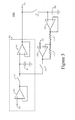
- S/H circuitry 300 of the present disclosure contains S/H subcircuit 302 which is substantially similar to the S/H circuit 100 in Figure 1 .
- the S/H subcircuit 302 takes an input voltage at input terminal 320 of the S/H circuitry 300 and produces a sample-and-held output at output terminal 321 of the S/H circuitry 300.
- the S/H subcircuit 302 includes input buffer circuit 310, hold capacitor 301 coupled via sampling switch 305 to the input buffer 310, and output buffer 315.
- the input buffer 310 may be implemented as an operational amplifier having a non-inverting input coupled to an input terminal 320 of the S/H circuitry 300, and an output coupled to an inverting input.
- the output buffer 315 may be implemented as an operational amplifier having a non-inverting input coupled to the hold capacitor 301, and an output coupled to an inverting input and to the output terminal 321 of the S/H circuitry 300.
- the S/H circuitry 300 further incorporates a DA suppression circuit for suppressing DA of the hold capacitor 301.
- the DA suppression circuit includes an inverting operational amplifier 330 having an output connectable to the hold capacitor 301 via switch 335.
- An inverting input of the amplifier 330 is coupled via resistor 332 to the output of the amplifier 330, and is supplied with an output signal of a secondary S/H circuit including switch 325, hold capacitor 326, and output buffer 327.
- the switch 325 connects the hold capacitor 326 to the output terminal 321 of the S/H circuitry.
- the output buffer 327 may be implemented as an operational amplifier having an output coupled via resistor 333 to the inverting input of the amplifier 330.
- a non-inverting input of the buffer 327 is connectable to the output terminal 321 via the switch 325.
- An inverting input of the buffer 327 is connected to the output of the buffer 327.
- a non-inverting input of the inverting amplifier 330 may be supplied by a bias voltage from bias voltage terminal 331.
- the S/H circuitry 300 operates in track and hold phases of an S/H procedure using the S/H subcircuit 302.
- switch 305 when switch 305 is closed, the S/H circuitry 300 operates in the track phase, in which the input buffer 310 forces the voltage across the hold capacitor 301 to be equal to the input voltage at the input terminal 320.
- the output buffer 315 then causes the output voltage at the output terminal 321 to be equal to the hold capacitor voltage and thus the input voltage.
- the hold capacitor 301 In the hold phase, when the switch 305 is open, the hold capacitor 301 maintains the approximate voltage present at the sampling moment, and this voltage is provided at the output terminal 321. As discussed above, if the hold capacitor 301 has DA, the charge trapping mechanism represents storage of charge which retains information about voltages applied to the hold capacitor 301 at times before the sampling moment. As the hold phase progresses, that charge storage will affect the value of voltage on the hold capacitor, which will manifest as a deviation of the output voltage from the intended behavior.
- the switch 335 is open and the switch 325 is closed, applying the output voltage 321 to the capacitor 326, which is buffered by the buffer 327.
- the switch 325 is opened, storing the voltage on the capacitor 326.
- the amplifier 330 in conjunction with resistors 332 and 333, provides a voltage at its output which is negatively correlated with the voltage on the capacitor 326, optionally modified by the bias voltage supplied from the terminal 331.
- the S/H circuitry 300 then transitions from the hold phase to the countersoak phase by closing switch 335, thereby applying a voltage value across capacitor 301 which is negatively correlated with the voltage held by the capacitor 301 in the hold phase.
- the output voltage 321 is no longer equal to the value held by the capacitor 301 in the hold phase or to the input value at the input terminal 320.
- additional circuitry may be used, for example, to switch the input of buffer 315 to the input terminal 320.
- the switch 335 is opened and the switch 305 is closed, switching the S/H circuitry 300 to the track phase described above in conjunction with circuit 100.
- the input buffer 310 forces the voltage across the hold capacitor 301 to be equal to the voltage at the input terminal 320.
- the voltage at the output terminal 321 also becomes equal to the voltage at the input terminal 320.
- the effect of the countersoak phase is to quickly modify the charge corresponding to the DA of capacitor 301, to cause a counteracting short-timescale movement during the subsequent hold phase.
- Timing of the countersoak phase may be chosen relative to the lengths of the track and hold phases, as well as the ratio of resistors 332 and 333, to substantially eliminate the DA effect at the output 321.
- the addition of the countersoak phase to the system operation implies an overall change to the system timing.
- This modification may be of much smaller magnitude than is necessary to achieve a given improvement under the first known technique described above, since the short time-timescale DA effects will be dominated by the most recent stimulus.
- This advantage may be increased by choosing resistors 322 and 323 so as to provide a larger voltage across the capacitor 301 in the countersoak phase.
- the system of the present disclosure produces a cancellation term using the DA effect itself. This means that the required timings may be chosen without knowledge of the magnitude of the DA effect. More importantly, since the timings required for cancellation are substantially independent of the magnitude of DA effect, the cancellation is effective at all temperatures.
- a voltage value V 2 supplied to the hold capacitor in the countersoak phase may be negatively correlated with the voltage value V 1 held in the hold capacitor in the hold phase.
- V 2 (as a function of V 1 ) may obey the relationship ⁇ a b ⁇ v 1 ⁇ v 2 ⁇ d ⁇ v 1 ⁇ a + b 2 ⁇ ⁇ a b ⁇ v 2 ⁇ d ⁇ v 1 .
- the voltage value V 1 may have a non-unifonn distribution having mean ⁇ 1
- the DA-suppressing circuit may form a process producing the voltage value V 2 in a non-deterministic fashion such that it has a mean ⁇ 2 .
- the process should be such that the joint probability distribution of the first and second voltage P 12 ( V 1 , V 2 ) may obey the relationship ⁇ ⁇ - ⁇ ⁇ ⁇ v 1 ⁇ v 2 ⁇ P 12 v 1 ⁇ v 2 ⁇ d ⁇ v 1 ⁇ d ⁇ v 2 ⁇ ⁇ 1 ⁇ ⁇ 2 .
- the voltage value applied to the capacitor 301 in the countersoak phase may be simply proportional to the opposite polarity of the voltage value held by the capacitor 301 in the hold phase. For example, if a +4V value is held by the capacitor 301 in the hold phase, the capacitor 301 may be supplied with the voltage of -4V in the countersoak phase.
- This simple choice obeys the equations above substantially independent of the distribution of input voltages. However other choices can give further improvements. For example, while the simple scheme may have timings chosen to provide perfect cancellation of the memory from one held value to the next, there will remain a much smaller effect from the other previously held values. This secondary effect may be cancelled by the addition of a secondary S/H circuit which allows application of a voltage which is the opposite of the previous sample plus a smaller amount of the opposite of the sample before that.
- DA effect shows a non-linearity or temperature dependence after cancellation
- that effect may be accounted for by introducing a counteracting dependence in the voltage applied during the countersoak phase, for example, by replacing resistor 322 or 323 with a component having appropriate temperature dependence or non-linearity.
- any additional time which must be added for the countersoak phase is much more effective at reducing DA than simply increasing cycle time by adding track time.
- the length of time between hold phases is determined by factors other than necessary analog settling time in the track phase, for example time needed to switch channels.
- FIG 4 illustrates ADC circuit 400 operating with an added countersoak phase described above.
- the ADC circuit 400 is responsive to an analog input signal at input terminal 420 to produce an output digital signal at output terminal 421, and comprises ADC subcircuit 402 which contains the same elements with like numbering as the ADC circuit 200 of Figure 2 .
- the control signal is modified with respect to the control signals 223 in Figure 2 .
- the ADC subcircuit 402 includes array 401 of capacitors, and array 407 of switches corresponding to the capacitors 401. Also, the ADC subcircuit 402 includes comparator 415 and control logic 417.
- Each switch in the array 407 is controllable by a respective control signal 424 to couple first terminal of the respective capacitor 401 to the input terminal 420, reference voltage terminal 422, or ground terminal.
- Second terminals of the capacitors 401 are coupled to the input of comparator 415, and may be connected to ground by sampling switch 405.
- the output of the comparator 415 is coupled to the control logic 417 that produces the digital output signal at output terminal 421.
- the ADC circuit 400 comprises DA-suppressing subcircuit 425 that operates to modify a plurality of control signals 423 produced by the control logic 417 so as to form a plurality of respective control signals 424 that control the respective switches 407.
- the DA-suppressing subcircuit 425 includes a plurality of transparent latches 426 and a plurality of exclusive-OR gates 430. To maintain the clarity of the drawing, Figure 4 shows a single latch 426 and a single exclusive-OR gate 430. However, the number of the latches 426 and the number of the gates 430 in the subcircuit 425 corresponds to the number of switches 407 controlled by the respective control signals 424.
- Each transparent latch 426 has a latch-enable input L supplied by countersoak control signal 440, and a data input D supplied by the respective control signal 423 formed by the control logic 417.
- the countersoak control signal may be formed by the control logic 417 or by a separate control unit.
- An output Q of each latch 426 is coupled to a first input of the respective exclusive-OR gate 430, a second input of which is supplied with the countersoak control signal 440.
- the ADC circuit 400 operates in three phases.
- the first phase is an acquisition phase equivalent to the acquisition phase of the ADC circuit 200.
- the sampling switch 405 is closed, and the switches 407 are configured to couple the respective capacitors 401 to the input terminal 420.
- the countersoak control signal 440 is at a logic low level, placing the transparent latches 426 in a transparent state, and thereby making the control signals 424 substantially equivalent to the respective control signals 423.
- the second phase is a conversion phase equivalent to the conversion phase of the ADC circuit 200.
- the sampling switch 405 is open, and the switches 407 are controlled to connect the respective capacitors 401 to the reference voltage terminal 422 or to the ground terminal on the basis of the outputs of comparator 415, as determined by the control logic 417 in a successive-approximation process, ultimately determining the digital output signal at the terminal 421.
- the countersoak control signal 440 remains at a logic low level, placing the transparent latches 426 in a transparent state, and thereby making the control signals 424 substantially equivalent to the respective control signals 423.
- the ADC circuit 400 transitions to the countersoak phase.
- the sampling switch 405 is closed, connecting capacitors 401 to the ground terminal.
- the countersoak control signal 440 is set to a logic high level, causing each transparent latch 426 to hold the value of the respective control signal 423 which was determined at the end of the conversion phase.
- the exclusive-OR gates 430 then act to logically invert the held value, causing each control signal 424 to correspond to the digital complement of the value present at the end of the conversion phase. This applies an average voltage value across the capacitors 401 which is negatively correlated with the average voltage value across the capacitors during the conversion phase.
- the switches 407 may be controlled to charge the respective capacitors 401 to a fixed state before coupling them to the input terminal 420 for the subsequent acquisition phase.
- this operation of circuit 400 may produce complete cancellation with appropriate choice of timings, and require little to no additional cycle time. Also as in the circuit 300, the cancellation produced is effective substantially independent of the magnitude of DA effect, and therefore independent of temperature.
- This operation of the ADC circuit 400 may also attain the further improvements described in conjunction with circuit 300 by increasing the digital complexity of subcircuit 425.
- additional memory elements such as latches or flip-flops may be employed to allow compensation for previous conversions.
- control signals 423 are interpreted as a digital value
- the exclusive-OR gates 430 provide the simple arithmetic function of complement, independently of the representation employed. With appropriate consideration of the representation, further digital arithmetic such as adders and multipliers or transformations such as look-up tables may be employed to include additional compensation sources or correct for non-linearities by adjusting the value of the control signals 424.
- the ADC circuit 400 shows the application of the invention to the specific sampling ADC shown as the ADC subcircuit 402, similar improvements may be achieved by equivalent modifications to the switch control signals of other sampling ADCs having other configurations of capacitors and switches, or operating by techniques other than successive approximation.
- the subcircuit 402 has a particular sampling ADC structure which is of the SAR type, operating on a single-ended input in a specific range, with a specific configuration of capacitors and switches, substantially the same effect occurs in other implementations.
- the comparator 415 might be replaced by a multi-level single step ADC and residue amplifier in a pipelined converter, or the capacitor array 401 might be functionally separated into an input sampling capacitor and a digital-to-analog conversion section, and the like.
Landscapes
- Engineering & Computer Science (AREA)
- Theoretical Computer Science (AREA)
- Analogue/Digital Conversion (AREA)
Abstract
Description
- This application claims priority of
US provisional patent application No 61/979,139 - This disclosure relates generally to capacitive sample-and-hold (S/H) systems, and in particular, to reducing or eliminating dielectric absorption effects in the S/H systems.
- Dielectric absorption (DA) is a form of capacitor non-ideality wherein the capacitor has additional memory of its history (beyond its expected capacitance), and tends in the direction of trying to return to a previous value of voltage across it. This memory (also called soakage) is attributed to a charge which becomes trapped in the dielectric of the capacitor over time, and takes time to escape as well. As such, it varies substantially with the physical construction of the capacitor, both among discrete types, and various implementations available in integrated circuits. These charge-trapping mechanisms also often have large temperature dependencies, varying by an order of magnitude or more over typical integrated circuit operating temperature ranges.
- In the context of a system integrating a capacitive sample-and-hold (S/H), the DA of the hold capacitor causes the value of a given sample to trend towards the value of previous samples as it is held. A simplified example of such an S/H circuit is shown as
circuit 100 inFigure 1 . S/H circuit 100 takes an input voltage atinput terminal 120 and produces a sample-and-held output atoutput terminal 121.Input buffer 110 buffers the input voltage.Hold capacitor 101 is periodically connected to the buffered input bysampling switch 105.Output buffer 115 isolates thehold capacitor 101 from loads applied to theoutput terminal 121. - The circuit operates in two alternating phases. The first is a track phase during which
switch 105 is closed. In the track phase, theinput buffer 110 forces the voltage across thehold capacitor 101 to be equal to the input voltage.Output buffer 115 then causes theoutput voltage 121 to be equal to the hold capacitor voltage and thus the input voltage. - The circuit transitions from a track phase to a hold phase when
switch 105 is opened at a sampling moment. In the hold phase, the hold capacitor maintains the approximate voltage present at the sampling moment, and this voltage is presented at the output. If thehold capacitor 101 has DA, the charge trapping mechanism represents storage of charge which retains infonnation about voltages applied to the hold capacitor at times before the sampling moment. As the hold phase progresses, that charge storage will affect the value of voltage on the hold capacitor, which will manifest as a deviation of the output voltage from the intended behavior. - Where the S/H function is part of a sampling analog-to-digital converter (ADC), DA will cause the ADC's output for a given sample to be affected by the values of previous samples.
Figure 2 shows anexemplary ADC circuit 200 that includesvoltage input 220 anddigital code output 221. An array ofswitches 207 operates to couple an array ofcapacitors 201 to theinput 220,reference voltage terminal 222, or ground under the control ofrespective control signals 223 produced bycontrol logic 217. Thecapacitor array 201 is also coupled to the input ofcomparator 215, and may be connected to ground bysampling switch 205. - The
ADC circuit 200 operates as a successive-approximation (SAR) ADC in two primary phases. The first acquisition phase is analogous to the tracking phase of thecircuit 100. In this phase,sampling switch 205 is closed, andswitch array 207 is configured to couple thecapacitor array 201 toinput voltage 220. Thus, the capacitors ofarray 201 have the input voltage imposed across them. - The circuit transitions from the acquisition phase to the conversion phase (analogous to the hold phase of circuit 100) by opening
sampling switch 205 at a sampling moment.Switch array 207 is then operated to connectcapacitors 201 to thereference voltage terminal 222 or ground on the basis of the outputs ofcomparator 215, as determined bycontrol logic 217 in a successive approximation process, ultimately determining thedigital output 221. - During this conversion phase, the voltage presented to the comparator is determined by the voltage across the capacitors at the sampling moment and the voltage applied by
switches 207. Ifcapacitors 201 have DA, the charge trapping mechanism represents storage of charge which retains information about voltages applied to the capacitors at times before the sampling moment. As the conversion phase progresses, that charge storage will affect the value of voltage on presented to the comparator, which will cause a deviation of the output digital code from the ideal value. - In some applications, this effect may not be deleterious, particularly as DA is typically a fairly linear phenomenon. However, in any situation where the S/H is being multiplexed between channels, the DA causes a low-frequency crosstalk between the channels which may be limiting.
- A first known technique for reducing DA is typically present in any S/H design. The effect of DA from one sample upon the following sample is directly dependent upon the ratio of time in which the capacitor holds the input signal to the time in which it tracks the input signal. Thus, one may decrease the sample-to-sample memory by decreasing that ratio (i.e. increasing the track time relative to the hold time). Unfortunately, changing this ratio substantially requires large changes to the timing characteristics, for example slowing down an ADC's sample rate by a factor comparable to the factor of improvement in crosstalk, and in many cases such a timing compromise is unacceptable.
- A second known technique for reducing DA provides an analog cancellation term. For example, an explicit network of resistors and capacitors may be exposed to the same voltage stimuli as the hold capacitor. The resistors are chosen to model the long-term storage effects present in the hold capacitor due to DA, and then used to inject a small correction term into the primary signal path.
- A conceptually similar third technique may be used when the S/H circuit is part of an ADC. In particular, a digital record of previous conversion outputs can be kept, and used to adjust the digital output of the present conversion in a predetermined fashion.
- The second and third techniques suffer from the problem of attempting to cancel the DA effect with an unrelated external term. Given that the DA effect may vary dramatically with temperature, it is at best difficult to construct a term which provides good cancellation across a wide range of temperatures.
- Therefore, it would be desirable to develop a DA-suppressing technique that would avoid disadvantages of known techniques.
- In accordance with one aspect of the present disclosure, sample-and-hold (S/H) circuitry operating in track and hold phases comprises a first S/H circuit having a first hold capacitor at which a first voltage value is maintained in the hold phase, and a dielectric absorption (DA) - suppressing circuit connectable to the first hold capacitor for operating the S/H circuitry in an additional phase after completing the hold phase and before entering the track phase.
- The DA-suppressing circuit is configured to supply the first hold capacitor, during an operation in the additional phase, with a second voltage value that is negatively correlated with the first voltage value.
- In accordance with an exemplary embodiment, the DA-suppressing circuit may include an inverting amplifier having a first input responsive to the first voltage value and an output, and a first switching element for coupling the output of the inverting amplifier to the first holding capacitor after the hold phase so as to operate the S/H circuitry in the additional phase. The inverting amplifier may have a second input supplied with a bias voltage value.
- The DA-suppressing circuit may further include a second S/H circuit having an input coupled to an output of the first S/H circuit and an output coupled to the first input of the inverting amplifier.
- The second S/H circuit may include a second hold capacitor and a second switching element for coupling the second hold capacitor to the output of the first S/H circuit during the hold phase. The second switching element may be opened before a transition from the hold phase to the additional phase so as maintain the first voltage value at the second holding capacitor. The first switching element may be opened and the second switching element may be closed to switch the S/H circuitry from the additional phase to the track phase.
- In accordance with another aspect of the present disclosure, a sampling analog-to-digital converter operating in acquisition and conversion phases comprises an array of capacitors, an array of switches controllable to couple the capacitors of the array to sources of at least two different voltages during the conversion phase, applying a first average voltage value across the capacitors, and a dielectric absorption (DA) suppressing circuit for controlling the array of switches during an additional phase after completing the conversion phase and before entering the acquisition phase.
- The DA-suppressing circuit may be configured to control the switches to apply a second average voltage value across the capacitors. The second average voltage value is negatively correlated with the first average voltage value.
- The DA-suppressing circuit may have a first input responsive to multiple first control signals produced by the converter, and an output for producing multiple second control signals corresponding to the respective first control signals and supplied to the respective switches of the array to control the switches so as to apply the second average voltage value across the capacitors.
- The DA-suppressing circuit may further have a second input supplied with an enable signal asserted at a first logic level during the acquisition and conversion phases, and asserted at a second logic level during the additional phase. The DA-suppressing circuit may be configured to produce the second control signals having values substantially equivalent to values of the respective first control signals when the enable signal is at the first logic level, and to produce the second control signals having values logically inverted with respect to the values of the corresponding first control signals when the enable signal is at the second logic level.
- In an exemplary embodiment, the DA-suppressing circuit may include multiple exclusive OR gates having first inputs responsive to the respective first control signals, second inputs responsive to the enable signal, and outputs for producing the respective second control signals.
- The DA-suppressing circuit may further include multiple latches having outputs coupled to the first inputs of the respective exclusive OR gates, and having inputs responsive to the respective first control signals.
- Additional advantages and aspects of the disclosure will become readily apparent to those skilled in the art from the following detailed description, wherein embodiments of the present disclosure are shown and described, simply by way of illustration of the best mode contemplated for practicing the present disclosure. As will be described, the disclosure is capable of other and different embodiments, and its several details are susceptible of modification in various obvious respects, all without departing from the spirit of the disclosure. Accordingly, the drawings and description are to be regarded as illustrative in nature, and not as limitative.
- The following detailed description of the embodiments of the present disclosure can best be understood when read in conjunction with the following drawings, in which the features are not necessarily drawn to scale but rather are drawn as to best illustrate the pertinent features, wherein:
-
FIG. 1 illustrates a conventional sample-and-hold (S/H) circuit. -
FIG. 2 illustrates a conventional sampling analog-to-digital converter (ADC). -
FIG. 3 shows S/H circuitry of the present disclosure. -
FIG. 4 shows a sampling ADC of the present disclosure. - The present disclosure will be made using the specific examples of S/H circuitry and ADC presented below. However, the concept of the disclosure is applicable to various other modifications of the implementations discussed below.
- The present disclosure provides a technique for suppressing DA effects in an S/H system which is inherently self-referential, and may be accomplished with little or no timing overhead. As discussed below, the essence of the disclosed technique is to add a third "countersoak" phase between the hold phase and the track phase of the S/H procedure.
- An exemplary embodiment of S/
H circuitry 300 of the present disclosure is presented inFigure 3 . The S/H circuitry 300 contains S/H subcircuit 302 which is substantially similar to the S/H circuit 100 inFigure 1 . In particular, the S/H subcircuit 302 takes an input voltage atinput terminal 320 of the S/H circuitry 300 and produces a sample-and-held output atoutput terminal 321 of the S/H circuitry 300. The S/H subcircuit 302 includesinput buffer circuit 310,hold capacitor 301 coupled viasampling switch 305 to theinput buffer 310, and output buffer 315. Theinput buffer 310 may be implemented as an operational amplifier having a non-inverting input coupled to aninput terminal 320 of the S/H circuitry 300, and an output coupled to an inverting input. The output buffer 315 may be implemented as an operational amplifier having a non-inverting input coupled to thehold capacitor 301, and an output coupled to an inverting input and to theoutput terminal 321 of the S/H circuitry 300. - The S/
H circuitry 300 further incorporates a DA suppression circuit for suppressing DA of thehold capacitor 301. The DA suppression circuit includes an invertingoperational amplifier 330 having an output connectable to thehold capacitor 301 viaswitch 335. An inverting input of theamplifier 330 is coupled viaresistor 332 to the output of theamplifier 330, and is supplied with an output signal of a secondary S/Hcircuit including switch 325,hold capacitor 326, andoutput buffer 327. - The
switch 325 connects thehold capacitor 326 to theoutput terminal 321 of the S/H circuitry. Theoutput buffer 327 may be implemented as an operational amplifier having an output coupled viaresistor 333 to the inverting input of theamplifier 330. A non-inverting input of thebuffer 327 is connectable to theoutput terminal 321 via theswitch 325. An inverting input of thebuffer 327 is connected to the output of thebuffer 327. A non-inverting input of the invertingamplifier 330 may be supplied by a bias voltage frombias voltage terminal 331. - The S/
H circuitry 300 operates in track and hold phases of an S/H procedure using the S/H subcircuit 302. In particular, whenswitch 305 is closed, the S/H circuitry 300 operates in the track phase, in which theinput buffer 310 forces the voltage across thehold capacitor 301 to be equal to the input voltage at theinput terminal 320. The output buffer 315 then causes the output voltage at theoutput terminal 321 to be equal to the hold capacitor voltage and thus the input voltage. - In the hold phase, when the
switch 305 is open, thehold capacitor 301 maintains the approximate voltage present at the sampling moment, and this voltage is provided at theoutput terminal 321. As discussed above, if thehold capacitor 301 has DA, the charge trapping mechanism represents storage of charge which retains information about voltages applied to thehold capacitor 301 at times before the sampling moment. As the hold phase progresses, that charge storage will affect the value of voltage on the hold capacitor, which will manifest as a deviation of the output voltage from the intended behavior. - During the hold phase of the S/
H circuitry 300, theswitch 335 is open and theswitch 325 is closed, applying theoutput voltage 321 to thecapacitor 326, which is buffered by thebuffer 327. Before the end of the hold phase, theswitch 325 is opened, storing the voltage on thecapacitor 326. Theamplifier 330, in conjunction withresistors capacitor 326, optionally modified by the bias voltage supplied from the terminal 331. - The S/
H circuitry 300 then transitions from the hold phase to the countersoak phase by closingswitch 335, thereby applying a voltage value acrosscapacitor 301 which is negatively correlated with the voltage held by thecapacitor 301 in the hold phase. In the countersoak phase, theoutput voltage 321 is no longer equal to the value held by thecapacitor 301 in the hold phase or to the input value at theinput terminal 320. In applications where this is not acceptable, additional circuitry may be used, for example, to switch the input of buffer 315 to theinput terminal 320. - At the conclusion of the countersoak phase, the
switch 335 is opened and theswitch 305 is closed, switching the S/H circuitry 300 to the track phase described above in conjunction withcircuit 100. In the track phase, theinput buffer 310 forces the voltage across thehold capacitor 301 to be equal to the voltage at theinput terminal 320. The voltage at theoutput terminal 321 also becomes equal to the voltage at theinput terminal 320. - The effect of the countersoak phase is to quickly modify the charge corresponding to the DA of
capacitor 301, to cause a counteracting short-timescale movement during the subsequent hold phase. Timing of the countersoak phase may be chosen relative to the lengths of the track and hold phases, as well as the ratio ofresistors output 321. - As described, the addition of the countersoak phase to the system operation implies an overall change to the system timing. This modification may be of much smaller magnitude than is necessary to achieve a given improvement under the first known technique described above, since the short time-timescale DA effects will be dominated by the most recent stimulus. This advantage may be increased by choosing resistors 322 and 323 so as to provide a larger voltage across the
capacitor 301 in the countersoak phase. - Unlike the dissimilar cancellation terms produced by known techniques, the system of the present disclosure produces a cancellation term using the DA effect itself. This means that the required timings may be chosen without knowledge of the magnitude of the DA effect. More importantly, since the timings required for cancellation are substantially independent of the magnitude of DA effect, the cancellation is effective at all temperatures.
- A voltage value V2 supplied to the hold capacitor in the countersoak phase may be negatively correlated with the voltage value V1 held in the hold capacitor in the hold phase.
- In the limited case where the DA suppression circuit produces the voltage V2 deterministically from the voltage V1, and the voltage V1 is known or assumed to take on any value between a lower bound a and an upper bound b with equal probability, then V2 (as a function of V1) may obey the relationship

- In a more general case, the voltage value V1 may have a non-unifonn distribution having mean µ1, and the DA-suppressing circuit may form a process producing the voltage value V2 in a non-deterministic fashion such that it has a mean µ2. In such a case, the process should be such that the joint probability distribution of the first and second voltage P 12 (V 1, V 2) may obey the relationship

- In an example of the S/
H circuitry 300, the voltage value applied to thecapacitor 301 in the countersoak phase may be simply proportional to the opposite polarity of the voltage value held by thecapacitor 301 in the hold phase. For example, if a +4V value is held by thecapacitor 301 in the hold phase, thecapacitor 301 may be supplied with the voltage of -4V in the countersoak phase. This simple choice obeys the equations above substantially independent of the distribution of input voltages. However other choices can give further improvements. For example, while the simple scheme may have timings chosen to provide perfect cancellation of the memory from one held value to the next, there will remain a much smaller effect from the other previously held values. This secondary effect may be cancelled by the addition of a secondary S/H circuit which allows application of a voltage which is the opposite of the previous sample plus a smaller amount of the opposite of the sample before that. - Similarly, if the DA effect shows a non-linearity or temperature dependence after cancellation, that effect may be accounted for by introducing a counteracting dependence in the voltage applied during the countersoak phase, for example, by replacing resistor 322 or 323 with a component having appropriate temperature dependence or non-linearity.
- Also apparent is that any additional time which must be added for the countersoak phase is much more effective at reducing DA than simply increasing cycle time by adding track time. In some cases, the length of time between hold phases is determined by factors other than necessary analog settling time in the track phase, for example time needed to switch channels. Moreover, there will frequently already be a third period of resetting the hold capacitor between samples. In these cases, the addition of a countersoak period may not increase cycle times at all.
-
Figure 4 illustratesADC circuit 400 operating with an added countersoak phase described above. TheADC circuit 400 is responsive to an analog input signal atinput terminal 420 to produce an output digital signal atoutput terminal 421, and comprisesADC subcircuit 402 which contains the same elements with like numbering as theADC circuit 200 ofFigure 2 . However, the control signal is modified with respect to the control signals 223 inFigure 2 . - In particular, the
ADC subcircuit 402 includesarray 401 of capacitors, andarray 407 of switches corresponding to thecapacitors 401. Also, theADC subcircuit 402 includescomparator 415 andcontrol logic 417. - Each switch in the
array 407 is controllable by a respective control signal 424 to couple first terminal of therespective capacitor 401 to theinput terminal 420,reference voltage terminal 422, or ground terminal. Second terminals of thecapacitors 401 are coupled to the input ofcomparator 415, and may be connected to ground by samplingswitch 405. The output of thecomparator 415 is coupled to thecontrol logic 417 that produces the digital output signal atoutput terminal 421. - Further, the
ADC circuit 400 comprises DA-suppressingsubcircuit 425 that operates to modify a plurality ofcontrol signals 423 produced by thecontrol logic 417 so as to form a plurality ofrespective control signals 424 that control the respective switches 407. The DA-suppressingsubcircuit 425 includes a plurality oftransparent latches 426 and a plurality of exclusive-OR gates 430. To maintain the clarity of the drawing,Figure 4 shows asingle latch 426 and a single exclusive-OR gate 430. However, the number of thelatches 426 and the number of thegates 430 in thesubcircuit 425 corresponds to the number ofswitches 407 controlled by the respective control signals 424. - Each
transparent latch 426 has a latch-enable input L supplied bycountersoak control signal 440, and a data input D supplied by the respective control signal 423 formed by thecontrol logic 417. The countersoak control signal may be formed by thecontrol logic 417 or by a separate control unit. An output Q of eachlatch 426 is coupled to a first input of the respective exclusive-OR gate 430, a second input of which is supplied with thecountersoak control signal 440. - The
ADC circuit 400 operates in three phases. The first phase is an acquisition phase equivalent to the acquisition phase of theADC circuit 200. In this phase, thesampling switch 405 is closed, and theswitches 407 are configured to couple therespective capacitors 401 to theinput terminal 420. During the acquisition phase, thecountersoak control signal 440 is at a logic low level, placing thetransparent latches 426 in a transparent state, and thereby making the control signals 424 substantially equivalent to the respective control signals 423. - The second phase is a conversion phase equivalent to the conversion phase of the
ADC circuit 200. In this phase, thesampling switch 405 is open, and theswitches 407 are controlled to connect therespective capacitors 401 to thereference voltage terminal 422 or to the ground terminal on the basis of the outputs ofcomparator 415, as determined by thecontrol logic 417 in a successive-approximation process, ultimately determining the digital output signal at the terminal 421. During the conversion phase, the countersoak control signal 440 remains at a logic low level, placing thetransparent latches 426 in a transparent state, and thereby making the control signals 424 substantially equivalent to the respective control signals 423. - Following the completion of the conversion phase, the
ADC circuit 400 transitions to the countersoak phase. In this phase, thesampling switch 405 is closed, connectingcapacitors 401 to the ground terminal. Thecountersoak control signal 440 is set to a logic high level, causing eachtransparent latch 426 to hold the value of the respective control signal 423 which was determined at the end of the conversion phase. The exclusive-OR gates 430 then act to logically invert the held value, causing each control signal 424 to correspond to the digital complement of the value present at the end of the conversion phase. This applies an average voltage value across thecapacitors 401 which is negatively correlated with the average voltage value across the capacitors during the conversion phase. After the countersoak phase, theswitches 407 may be controlled to charge therespective capacitors 401 to a fixed state before coupling them to theinput terminal 420 for the subsequent acquisition phase. - As described in conjunction with the
circuit 300, this operation ofcircuit 400 may produce complete cancellation with appropriate choice of timings, and require little to no additional cycle time. Also as in thecircuit 300, the cancellation produced is effective substantially independent of the magnitude of DA effect, and therefore independent of temperature. - This operation of the
ADC circuit 400 may also attain the further improvements described in conjunction withcircuit 300 by increasing the digital complexity ofsubcircuit 425. For example, additional memory elements such as latches or flip-flops may be employed to allow compensation for previous conversions. - If the control signals 423 are interpreted as a digital value, the exclusive-
OR gates 430 provide the simple arithmetic function of complement, independently of the representation employed. With appropriate consideration of the representation, further digital arithmetic such as adders and multipliers or transformations such as look-up tables may be employed to include additional compensation sources or correct for non-linearities by adjusting the value of the control signals 424. - While the
ADC circuit 400 shows the application of the invention to the specific sampling ADC shown as theADC subcircuit 402, similar improvements may be achieved by equivalent modifications to the switch control signals of other sampling ADCs having other configurations of capacitors and switches, or operating by techniques other than successive approximation. While thesubcircuit 402 has a particular sampling ADC structure which is of the SAR type, operating on a single-ended input in a specific range, with a specific configuration of capacitors and switches, substantially the same effect occurs in other implementations. For example, thecomparator 415 might be replaced by a multi-level single step ADC and residue amplifier in a pipelined converter, or thecapacitor array 401 might be functionally separated into an input sampling capacitor and a digital-to-analog conversion section, and the like. - The foregoing description illustrates and describes aspects of the present invention. Additionally, the disclosure shows and describes only preferred embodiments, but as aforementioned, it is to be understood that the invention is capable of use in various other combinations, modifications, and environments and is capable of changes or modifications within the scope of the inventive concept as expressed herein, commensurate with the above teachings, and/or the skill or knowledge of the relevant art.
- The embodiments described hereinabove are further intended to explain best modes known of practicing the invention and to enable others skilled in the art to utilize the invention in such, or other, embodiments and with the various modifications required by the particular applications or uses of the invention. Accordingly, the description is not intended to limit the invention to the form disclosed herein.
Claims (13)
- Sample-and-hold (S/H) circuitry operating in track and hold phases, and comprising:a first S/H circuit having a first hold capacitor at which a first voltage value is maintained in the hold phase, anda dielectric absorption (DA)- suppressing circuit connectable to the first hold capacitor for operating the S/H circuitry in an additional phase after completing the hold phase and before entering the track phase,the DA-suppressing circuit being configured to supply the first hold capacitor, during an operation in the additional phase, with a second voltage value which is negatively correlated with the first voltage value.
- The S/H circuitry of claim 1, wherein the DA-suppressing circuit includes:an inverting amplifier having a first input responsive to the first voltage value and an output, anda first switching element for coupling the output of the inverting amplifier to the first holding capacitor after the hold phase so as to operate the S/H circuitry in the additional phase.
- The S/H circuitry of claim 2, wherein the inverting amplifier has a second input supplied with a bias voltage value.
- The S/H circuitry of claim 2 or 3, wherein the DA-suppressing circuit further includes a second S/H circuit having an input coupled to an output of the first S/H circuit and an output coupled to the first input of the inverting amplifier.
- The S/H circuitry of claim 4, wherein the second S/H circuit includes a second hold capacitor and a second switching element for coupling the second hold capacitor to the output of the first S/H circuit during the hold phase.
- The S/H circuitry of claim 5, wherein the second switching element is opened before a transition from the hold phase to the additional phase so as maintain the first voltage value at the second holding capacitor.
- The S/H circuitry of claim 5 or 6, wherein the first switching element is opened and the second switching element is closed to switch the S/H circuitry from the additional phase to the track phase.
- A sampling analog-to-digital converter operating in acquisition and conversion phases and comprising:an array of capacitors,an array of switches controllable to couple the capacitors of the array to sources of at least two different voltages during the conversion phase, applying a first average voltage value across the capacitors, anda dielectric absorbtion (DA) - suppressing circuit for controlling the array of switches during an additional phase after completing the conversion phase and before entering the acquisition phase,the DA-suppressing circuit being configured to control the switches to apply a second average voltage value across the capacitors, the second average voltage value being negatively correlated with the first average voltage value.
- The converter of claim 8, wherein the DA-suppressing circuit has a first input responsive to multiple first control signals produced by the converter, and an output for producing multiple second control signals corresponding to the respective first control signals and supplied to the respective switches of the array to control the switches so as to apply the second average voltage value across the capacitors.
- The converter of claim 8 or 9, wherein the DA-suppressing circuit further has a second input supplied with an enable signal asserted at a first logic level during the acquisition and conversion phases, and asserted at a second logic level during the additional phase.
- The converter of claim 10, wherein the DA-suppressing circuit is configured to produce the second control signals having values substantially equivalent to values of the respective first control signals when the enable signal is at the first logic level, and to produce the second control signals having values logically inverted with respect to the values of the corresponding first control signals when the enable signal is at the second logic level.
- The converter of any one of claims 9 to 11, wherein the DA-suppressing circuit further includes multiple latches having inputs responsive to the respective first control signals.
- The converter of claim 12, wherein the DA-suppressing circuit includes multiple exclusive OR gates having first inputs coupled to the outputs of the respective latches, second inputs responsive to the enable signal, and outputs for producing the respective second control signals.
Applications Claiming Priority (2)
| Application Number | Priority Date | Filing Date | Title |
|---|---|---|---|
| US201461979139P | 2014-04-14 | 2014-04-14 | |
| US14/472,160 US9197235B2 (en) | 2014-04-14 | 2014-08-28 | Suppressing dielectric absorption effects in sample-and-hold systems |
Publications (2)
| Publication Number | Publication Date |
|---|---|
| EP2933800A1 true EP2933800A1 (en) | 2015-10-21 |
| EP2933800B1 EP2933800B1 (en) | 2020-08-19 |
Family
ID=53015463
Family Applications (1)
| Application Number | Title | Priority Date | Filing Date |
|---|---|---|---|
| EP15001050.2A Active EP2933800B1 (en) | 2014-04-14 | 2015-04-13 | Suppressing dielectric absorption effects in sample-and-hold systems |
Country Status (2)
| Country | Link |
|---|---|
| US (1) | US9197235B2 (en) |
| EP (1) | EP2933800B1 (en) |
Families Citing this family (2)
| Publication number | Priority date | Publication date | Assignee | Title |
|---|---|---|---|---|
| US10256831B2 (en) | 2016-09-21 | 2019-04-09 | Analog Devices Global | Method and apparatus to reduce effect of dielectric absorption in SAR ADC |
| WO2019109363A1 (en) * | 2017-12-09 | 2019-06-13 | Dongguan Bang Bang Tang Electronic Technologies Co., Ltd. | Current sensor for biomedical measurements |
Citations (2)
| Publication number | Priority date | Publication date | Assignee | Title |
|---|---|---|---|---|
| US4211981A (en) * | 1978-05-04 | 1980-07-08 | Abbott Laboratories | Integrator with dielectric absorption correction |
| EP2246985A1 (en) * | 2009-04-27 | 2010-11-03 | Linear Technology Corporation | Complex-admittance digital-to-analog converter |
Family Cites Families (6)
| Publication number | Priority date | Publication date | Assignee | Title |
|---|---|---|---|---|
| US4023097A (en) * | 1975-11-21 | 1977-05-10 | Datatron, Inc. | Noise and dielectric absorption compensation circuit |
| US5519328A (en) * | 1994-10-28 | 1996-05-21 | Keithley Instruments, Inc. | Compensation for dielectric absorption effect |
| US5557242A (en) * | 1995-05-22 | 1996-09-17 | Motorola, Inc. | Method and apparatus for dielectric absorption compensation |
| US6294945B1 (en) * | 2000-02-02 | 2001-09-25 | National Instruments Corporation | System and method for compensating the dielectric absorption of a capacitor using the dielectric absorption of another capacitor |
| US7095280B2 (en) * | 2004-08-16 | 2006-08-22 | National Instruments Corporation | Programmable gain instrumentation amplifier having improved dielectric absorption compensation and common mode rejection ratio |
| US9122289B2 (en) * | 2012-12-03 | 2015-09-01 | Dialog Semiconductor Gmbh | Circuit to control the effect of dielectric absorption in dynamic voltage scaling low dropout regulator |
-
2014
- 2014-08-28 US US14/472,160 patent/US9197235B2/en active Active
-
2015
- 2015-04-13 EP EP15001050.2A patent/EP2933800B1/en active Active
Patent Citations (2)
| Publication number | Priority date | Publication date | Assignee | Title |
|---|---|---|---|---|
| US4211981A (en) * | 1978-05-04 | 1980-07-08 | Abbott Laboratories | Integrator with dielectric absorption correction |
| EP2246985A1 (en) * | 2009-04-27 | 2010-11-03 | Linear Technology Corporation | Complex-admittance digital-to-analog converter |
Also Published As
| Publication number | Publication date |
|---|---|
| US20150295588A1 (en) | 2015-10-15 |
| US9197235B2 (en) | 2015-11-24 |
| EP2933800B1 (en) | 2020-08-19 |
Similar Documents
| Publication | Publication Date | Title |
|---|---|---|
| US8994564B2 (en) | Analog to digital converter including a pre-charge circuit | |
| CN105281773B (en) | System and method for multi-channel sampling SAR ADC | |
| US8912940B2 (en) | String DAC charge boost system and method | |
| US10187077B2 (en) | Precharge switch-capacitor circuit and method | |
| CN105720980B (en) | SAR DAC with dedicated reference capacitor for each bit capacitor | |
| US8497795B2 (en) | Differential successive approximation analog to digital converter | |
| EP2918014B1 (en) | Analog to digital conversion method with offset tracking and correction and analog to digital converter implementing the same | |
| DE102015121472A1 (en) | SAR ADCS WITH DEDICATED REFERENCE CAPACITOR FOR EACH BIT CAPACITOR | |
| US20140218223A1 (en) | Multiplexed sigma delta modulator | |
| US10972118B1 (en) | Successive-approximation analog-to-digital converter gain calibration using floating capacitors | |
| US11012084B1 (en) | Self-calibrating successive-approximation analog-to-digital converters | |
| US10715167B2 (en) | Control circuit and control method of successive approximation register analog-to-digital converter | |
| JP2560478B2 (en) | Analog-digital converter | |
| US9197235B2 (en) | Suppressing dielectric absorption effects in sample-and-hold systems | |
| US10630310B1 (en) | Analog signal generation by hardware re-use in sampled circuits | |
| US4989002A (en) | Common-mode error self-calibration circuit and method of operation | |
| KR101746064B1 (en) | Successive approximation register analog to digital converter | |
| US10038452B2 (en) | Incremental preloading in an analog-to-digital converter | |
| KR890011222A (en) | Sequential Analog-to-Digital Converter | |
| US7420499B2 (en) | Analog-to-digital converter and threshold-value correcting method | |
| US6198313B1 (en) | Infinite sample-and-hold circuit | |
| US9935649B1 (en) | Low power quantizer with passive summers and interpolated dynamic comparators | |
| US10972120B1 (en) | Monotonicity self-testing for analog-to-digital converters | |
| JPH09162659A (en) | Integrated circuit including current copying machine, current copying machine and current copying method | |
| US20090212830A1 (en) | Buffer device for switched capacitance circuit |
Legal Events
| Date | Code | Title | Description |
|---|---|---|---|
| PUAI | Public reference made under article 153(3) epc to a published international application that has entered the european phase |
Free format text: ORIGINAL CODE: 0009012 |
|
| AK | Designated contracting states |
Kind code of ref document: A1 Designated state(s): AL AT BE BG CH CY CZ DE DK EE ES FI FR GB GR HR HU IE IS IT LI LT LU LV MC MK MT NL NO PL PT RO RS SE SI SK SM TR |
|
| AX | Request for extension of the european patent |
Extension state: BA ME |
|
| 17P | Request for examination filed |
Effective date: 20160421 |
|
| RBV | Designated contracting states (corrected) |
Designated state(s): AL AT BE BG CH CY CZ DE DK EE ES FI FR GB GR HR HU IE IS IT LI LT LU LV MC MK MT NL NO PL PT RO RS SE SI SK SM TR |
|
| STAA | Information on the status of an ep patent application or granted ep patent |
Free format text: STATUS: EXAMINATION IS IN PROGRESS |
|
| 17Q | First examination report despatched |
Effective date: 20180315 |
|
| GRAP | Despatch of communication of intention to grant a patent |
Free format text: ORIGINAL CODE: EPIDOSNIGR1 |
|
| STAA | Information on the status of an ep patent application or granted ep patent |
Free format text: STATUS: GRANT OF PATENT IS INTENDED |
|
| RIC1 | Information provided on ipc code assigned before grant |
Ipc: H03G 1/00 20060101ALI20200204BHEP Ipc: G11C 27/02 20060101AFI20200204BHEP Ipc: H03M 1/46 20060101ALI20200204BHEP Ipc: H03M 1/12 20060101ALI20200204BHEP |
|
| INTG | Intention to grant announced |
Effective date: 20200224 |
|
| GRAJ | Information related to disapproval of communication of intention to grant by the applicant or resumption of examination proceedings by the epo deleted |
Free format text: ORIGINAL CODE: EPIDOSDIGR1 |
|
| STAA | Information on the status of an ep patent application or granted ep patent |
Free format text: STATUS: EXAMINATION IS IN PROGRESS |
|
| GRAR | Information related to intention to grant a patent recorded |
Free format text: ORIGINAL CODE: EPIDOSNIGR71 |
|
| GRAS | Grant fee paid |
Free format text: ORIGINAL CODE: EPIDOSNIGR3 |
|
| STAA | Information on the status of an ep patent application or granted ep patent |
Free format text: STATUS: GRANT OF PATENT IS INTENDED |
|
| GRAA | (expected) grant |
Free format text: ORIGINAL CODE: 0009210 |
|
| STAA | Information on the status of an ep patent application or granted ep patent |
Free format text: STATUS: THE PATENT HAS BEEN GRANTED |
|
| INTG | Intention to grant announced |
Effective date: 20200709 |
|
| AK | Designated contracting states |
Kind code of ref document: B1 Designated state(s): AL AT BE BG CH CY CZ DE DK EE ES FI FR GB GR HR HU IE IS IT LI LT LU LV MC MK MT NL NO PL PT RO RS SE SI SK SM TR |
|
| REG | Reference to a national code |
Ref country code: CH Ref legal event code: EP |
|
| REG | Reference to a national code |
Ref country code: DE Ref legal event code: R096 Ref document number: 602015057584 Country of ref document: DE |
|
| REG | Reference to a national code |
Ref country code: AT Ref legal event code: REF Ref document number: 1304860 Country of ref document: AT Kind code of ref document: T Effective date: 20200915 |
|
| REG | Reference to a national code |
Ref country code: IE Ref legal event code: FG4D |
|
| REG | Reference to a national code |
Ref country code: LT Ref legal event code: MG4D |
|
| REG | Reference to a national code |
Ref country code: NL Ref legal event code: MP Effective date: 20200819 |
|
| PG25 | Lapsed in a contracting state [announced via postgrant information from national office to epo] |
Ref country code: FI Free format text: LAPSE BECAUSE OF FAILURE TO SUBMIT A TRANSLATION OF THE DESCRIPTION OR TO PAY THE FEE WITHIN THE PRESCRIBED TIME-LIMIT Effective date: 20200819 Ref country code: SE Free format text: LAPSE BECAUSE OF FAILURE TO SUBMIT A TRANSLATION OF THE DESCRIPTION OR TO PAY THE FEE WITHIN THE PRESCRIBED TIME-LIMIT Effective date: 20200819 Ref country code: HR Free format text: LAPSE BECAUSE OF FAILURE TO SUBMIT A TRANSLATION OF THE DESCRIPTION OR TO PAY THE FEE WITHIN THE PRESCRIBED TIME-LIMIT Effective date: 20200819 Ref country code: BG Free format text: LAPSE BECAUSE OF FAILURE TO SUBMIT A TRANSLATION OF THE DESCRIPTION OR TO PAY THE FEE WITHIN THE PRESCRIBED TIME-LIMIT Effective date: 20201119 Ref country code: PT Free format text: LAPSE BECAUSE OF FAILURE TO SUBMIT A TRANSLATION OF THE DESCRIPTION OR TO PAY THE FEE WITHIN THE PRESCRIBED TIME-LIMIT Effective date: 20201221 Ref country code: LT Free format text: LAPSE BECAUSE OF FAILURE TO SUBMIT A TRANSLATION OF THE DESCRIPTION OR TO PAY THE FEE WITHIN THE PRESCRIBED TIME-LIMIT Effective date: 20200819 Ref country code: GR Free format text: LAPSE BECAUSE OF FAILURE TO SUBMIT A TRANSLATION OF THE DESCRIPTION OR TO PAY THE FEE WITHIN THE PRESCRIBED TIME-LIMIT Effective date: 20201120 Ref country code: NO Free format text: LAPSE BECAUSE OF FAILURE TO SUBMIT A TRANSLATION OF THE DESCRIPTION OR TO PAY THE FEE WITHIN THE PRESCRIBED TIME-LIMIT Effective date: 20201119 |
|
| REG | Reference to a national code |
Ref country code: AT Ref legal event code: MK05 Ref document number: 1304860 Country of ref document: AT Kind code of ref document: T Effective date: 20200819 |
|
| PG25 | Lapsed in a contracting state [announced via postgrant information from national office to epo] |
Ref country code: NL Free format text: LAPSE BECAUSE OF FAILURE TO SUBMIT A TRANSLATION OF THE DESCRIPTION OR TO PAY THE FEE WITHIN THE PRESCRIBED TIME-LIMIT Effective date: 20200819 Ref country code: LV Free format text: LAPSE BECAUSE OF FAILURE TO SUBMIT A TRANSLATION OF THE DESCRIPTION OR TO PAY THE FEE WITHIN THE PRESCRIBED TIME-LIMIT Effective date: 20200819 Ref country code: RS Free format text: LAPSE BECAUSE OF FAILURE TO SUBMIT A TRANSLATION OF THE DESCRIPTION OR TO PAY THE FEE WITHIN THE PRESCRIBED TIME-LIMIT Effective date: 20200819 Ref country code: PL Free format text: LAPSE BECAUSE OF FAILURE TO SUBMIT A TRANSLATION OF THE DESCRIPTION OR TO PAY THE FEE WITHIN THE PRESCRIBED TIME-LIMIT Effective date: 20200819 Ref country code: IS Free format text: LAPSE BECAUSE OF FAILURE TO SUBMIT A TRANSLATION OF THE DESCRIPTION OR TO PAY THE FEE WITHIN THE PRESCRIBED TIME-LIMIT Effective date: 20201219 |
|
| PG25 | Lapsed in a contracting state [announced via postgrant information from national office to epo] |
Ref country code: CZ Free format text: LAPSE BECAUSE OF FAILURE TO SUBMIT A TRANSLATION OF THE DESCRIPTION OR TO PAY THE FEE WITHIN THE PRESCRIBED TIME-LIMIT Effective date: 20200819 Ref country code: DK Free format text: LAPSE BECAUSE OF FAILURE TO SUBMIT A TRANSLATION OF THE DESCRIPTION OR TO PAY THE FEE WITHIN THE PRESCRIBED TIME-LIMIT Effective date: 20200819 Ref country code: EE Free format text: LAPSE BECAUSE OF FAILURE TO SUBMIT A TRANSLATION OF THE DESCRIPTION OR TO PAY THE FEE WITHIN THE PRESCRIBED TIME-LIMIT Effective date: 20200819 Ref country code: SM Free format text: LAPSE BECAUSE OF FAILURE TO SUBMIT A TRANSLATION OF THE DESCRIPTION OR TO PAY THE FEE WITHIN THE PRESCRIBED TIME-LIMIT Effective date: 20200819 Ref country code: RO Free format text: LAPSE BECAUSE OF FAILURE TO SUBMIT A TRANSLATION OF THE DESCRIPTION OR TO PAY THE FEE WITHIN THE PRESCRIBED TIME-LIMIT Effective date: 20200819 |
|
| REG | Reference to a national code |
Ref country code: DE Ref legal event code: R097 Ref document number: 602015057584 Country of ref document: DE |
|
| REG | Reference to a national code |
Ref country code: DE Ref legal event code: R082 Ref document number: 602015057584 Country of ref document: DE Representative=s name: MUELLER-BORE & PARTNER PATENTANWAELTE PARTG MB, DE Ref country code: DE Ref legal event code: R081 Ref document number: 602015057584 Country of ref document: DE Owner name: ANALOG DEVICES INTERNATIONAL UNLIMITED COMPANY, IE Free format text: FORMER OWNER: LINEAR TECHNOLOGY CORPORATION, MILPITAS, CALIF., US Ref country code: DE Ref legal event code: R082 Ref document number: 602015057584 Country of ref document: DE Representative=s name: WITHERS & ROGERS LLP, DE |
|
| PG25 | Lapsed in a contracting state [announced via postgrant information from national office to epo] |
Ref country code: AL Free format text: LAPSE BECAUSE OF FAILURE TO SUBMIT A TRANSLATION OF THE DESCRIPTION OR TO PAY THE FEE WITHIN THE PRESCRIBED TIME-LIMIT Effective date: 20200819 Ref country code: AT Free format text: LAPSE BECAUSE OF FAILURE TO SUBMIT A TRANSLATION OF THE DESCRIPTION OR TO PAY THE FEE WITHIN THE PRESCRIBED TIME-LIMIT Effective date: 20200819 Ref country code: ES Free format text: LAPSE BECAUSE OF FAILURE TO SUBMIT A TRANSLATION OF THE DESCRIPTION OR TO PAY THE FEE WITHIN THE PRESCRIBED TIME-LIMIT Effective date: 20200819 |
|
| PLBE | No opposition filed within time limit |
Free format text: ORIGINAL CODE: 0009261 |
|
| STAA | Information on the status of an ep patent application or granted ep patent |
Free format text: STATUS: NO OPPOSITION FILED WITHIN TIME LIMIT |
|
| PG25 | Lapsed in a contracting state [announced via postgrant information from national office to epo] |
Ref country code: SK Free format text: LAPSE BECAUSE OF FAILURE TO SUBMIT A TRANSLATION OF THE DESCRIPTION OR TO PAY THE FEE WITHIN THE PRESCRIBED TIME-LIMIT Effective date: 20200819 |
|
| REG | Reference to a national code |
Ref country code: DE Ref legal event code: R082 Ref document number: 602015057584 Country of ref document: DE Representative=s name: WITHERS & ROGERS LLP, DE |
|
| 26N | No opposition filed |
Effective date: 20210520 |
|
| PG25 | Lapsed in a contracting state [announced via postgrant information from national office to epo] |
Ref country code: IT Free format text: LAPSE BECAUSE OF FAILURE TO SUBMIT A TRANSLATION OF THE DESCRIPTION OR TO PAY THE FEE WITHIN THE PRESCRIBED TIME-LIMIT Effective date: 20200819 |
|
| PG25 | Lapsed in a contracting state [announced via postgrant information from national office to epo] |
Ref country code: SI Free format text: LAPSE BECAUSE OF FAILURE TO SUBMIT A TRANSLATION OF THE DESCRIPTION OR TO PAY THE FEE WITHIN THE PRESCRIBED TIME-LIMIT Effective date: 20200819 |
|
| PG25 | Lapsed in a contracting state [announced via postgrant information from national office to epo] |
Ref country code: MC Free format text: LAPSE BECAUSE OF FAILURE TO SUBMIT A TRANSLATION OF THE DESCRIPTION OR TO PAY THE FEE WITHIN THE PRESCRIBED TIME-LIMIT Effective date: 20200819 |
|
| REG | Reference to a national code |
Ref country code: GB Ref legal event code: 732E Free format text: REGISTERED BETWEEN 20211125 AND 20211201 |
|
| PG25 | Lapsed in a contracting state [announced via postgrant information from national office to epo] |
Ref country code: LU Free format text: LAPSE BECAUSE OF NON-PAYMENT OF DUE FEES Effective date: 20210413 |
|
| REG | Reference to a national code |
Ref country code: BE Ref legal event code: MM Effective date: 20210430 |
|
| PG25 | Lapsed in a contracting state [announced via postgrant information from national office to epo] |
Ref country code: LI Free format text: LAPSE BECAUSE OF NON-PAYMENT OF DUE FEES Effective date: 20210430 Ref country code: CH Free format text: LAPSE BECAUSE OF NON-PAYMENT OF DUE FEES Effective date: 20210430 |
|
| PG25 | Lapsed in a contracting state [announced via postgrant information from national office to epo] |
Ref country code: IE Free format text: LAPSE BECAUSE OF NON-PAYMENT OF DUE FEES Effective date: 20210413 |
|
| PG25 | Lapsed in a contracting state [announced via postgrant information from national office to epo] |
Ref country code: IS Free format text: LAPSE BECAUSE OF FAILURE TO SUBMIT A TRANSLATION OF THE DESCRIPTION OR TO PAY THE FEE WITHIN THE PRESCRIBED TIME-LIMIT Effective date: 20201219 |
|
| PG25 | Lapsed in a contracting state [announced via postgrant information from national office to epo] |
Ref country code: BE Free format text: LAPSE BECAUSE OF NON-PAYMENT OF DUE FEES Effective date: 20210430 |
|
| PG25 | Lapsed in a contracting state [announced via postgrant information from national office to epo] |
Ref country code: HU Free format text: LAPSE BECAUSE OF FAILURE TO SUBMIT A TRANSLATION OF THE DESCRIPTION OR TO PAY THE FEE WITHIN THE PRESCRIBED TIME-LIMIT; INVALID AB INITIO Effective date: 20150413 |
|
| PG25 | Lapsed in a contracting state [announced via postgrant information from national office to epo] |
Ref country code: CY Free format text: LAPSE BECAUSE OF FAILURE TO SUBMIT A TRANSLATION OF THE DESCRIPTION OR TO PAY THE FEE WITHIN THE PRESCRIBED TIME-LIMIT Effective date: 20200819 |
|
| PG25 | Lapsed in a contracting state [announced via postgrant information from national office to epo] |
Ref country code: MK Free format text: LAPSE BECAUSE OF FAILURE TO SUBMIT A TRANSLATION OF THE DESCRIPTION OR TO PAY THE FEE WITHIN THE PRESCRIBED TIME-LIMIT Effective date: 20200819 |
|
| PG25 | Lapsed in a contracting state [announced via postgrant information from national office to epo] |
Ref country code: MT Free format text: LAPSE BECAUSE OF FAILURE TO SUBMIT A TRANSLATION OF THE DESCRIPTION OR TO PAY THE FEE WITHIN THE PRESCRIBED TIME-LIMIT Effective date: 20200819 |
|
| PGFP | Annual fee paid to national office [announced via postgrant information from national office to epo] |
Ref country code: DE Payment date: 20250319 Year of fee payment: 11 |
|
| PG25 | Lapsed in a contracting state [announced via postgrant information from national office to epo] |
Ref country code: TR Free format text: LAPSE BECAUSE OF FAILURE TO SUBMIT A TRANSLATION OF THE DESCRIPTION OR TO PAY THE FEE WITHIN THE PRESCRIBED TIME-LIMIT Effective date: 20200819 |
|
| PGFP | Annual fee paid to national office [announced via postgrant information from national office to epo] |
Ref country code: GB Payment date: 20260319 Year of fee payment: 12 |
|
| PGFP | Annual fee paid to national office [announced via postgrant information from national office to epo] |
Ref country code: FR Payment date: 20260320 Year of fee payment: 12 |