EP2930855A1 - Mechanical enclosures for a communication device - Google Patents
Mechanical enclosures for a communication device Download PDFInfo
- Publication number
- EP2930855A1 EP2930855A1 EP15163114.0A EP15163114A EP2930855A1 EP 2930855 A1 EP2930855 A1 EP 2930855A1 EP 15163114 A EP15163114 A EP 15163114A EP 2930855 A1 EP2930855 A1 EP 2930855A1
- Authority
- EP
- European Patent Office
- Prior art keywords
- conductive
- conductive regions
- conductive region
- bottom enclosure
- communication device
- Prior art date
- Legal status (The legal status is an assumption and is not a legal conclusion. Google has not performed a legal analysis and makes no representation as to the accuracy of the status listed.)
- Granted
Links
Images




Classifications
-
- H—ELECTRICITY
- H04—ELECTRIC COMMUNICATION TECHNIQUE
- H04W—WIRELESS COMMUNICATION NETWORKS
- H04W4/00—Services specially adapted for wireless communication networks; Facilities therefor
- H04W4/80—Services using short range communication, e.g. near-field communication [NFC], radio-frequency identification [RFID] or low energy communication
-
- H—ELECTRICITY
- H04—ELECTRIC COMMUNICATION TECHNIQUE
- H04B—TRANSMISSION
- H04B1/00—Details of transmission systems, not covered by a single one of groups H04B3/00 - H04B13/00; Details of transmission systems not characterised by the medium used for transmission
- H04B1/38—Transceivers, i.e. devices in which transmitter and receiver form a structural unit and in which at least one part is used for functions of transmitting and receiving
- H04B1/3827—Portable transceivers
- H04B1/3888—Arrangements for carrying or protecting transceivers
-
- H—ELECTRICITY
- H04—ELECTRIC COMMUNICATION TECHNIQUE
- H04B—TRANSMISSION
- H04B5/00—Near-field transmission systems, e.g. inductive or capacitive transmission systems
- H04B5/20—Near-field transmission systems, e.g. inductive or capacitive transmission systems characterised by the transmission technique; characterised by the transmission medium
- H04B5/24—Inductive coupling
-
- H—ELECTRICITY
- H04—ELECTRIC COMMUNICATION TECHNIQUE
- H04B—TRANSMISSION
- H04B5/00—Near-field transmission systems, e.g. inductive or capacitive transmission systems
- H04B5/40—Near-field transmission systems, e.g. inductive or capacitive transmission systems characterised by components specially adapted for near-field transmission
- H04B5/45—Transponders
-
- H—ELECTRICITY
- H04—ELECTRIC COMMUNICATION TECHNIQUE
- H04B—TRANSMISSION
- H04B5/00—Near-field transmission systems, e.g. inductive or capacitive transmission systems
- H04B5/70—Near-field transmission systems, e.g. inductive or capacitive transmission systems specially adapted for specific purposes
- H04B5/79—Near-field transmission systems, e.g. inductive or capacitive transmission systems specially adapted for specific purposes for data transfer in combination with power transfer
-
- H—ELECTRICITY
- H04—ELECTRIC COMMUNICATION TECHNIQUE
- H04L—TRANSMISSION OF DIGITAL INFORMATION, e.g. TELEGRAPHIC COMMUNICATION
- H04L67/00—Network arrangements or protocols for supporting network services or applications
- H04L67/01—Protocols
- H04L67/12—Protocols specially adapted for proprietary or special-purpose networking environments, e.g. medical networks, sensor networks, networks in vehicles or remote metering networks
Definitions
- the present disclosure generally relates to a communication device and including a mechanical chassis of the communication device.
- NFC near field communication
- the credit information provided by these credit cards can be loaded and stored onto an NFC enabled device to be used as needed.
- the NFC enabled device is simply tapped to a credit card terminal to relay the credit information to complete a transaction.
- a ticket writing system such as those used in bus and train terminals, may simply write ticket fare information onto the NFC enabled device instead of providing a paper ticket to a passenger. The passenger simply taps the NFC enabled device to a reader to ride the bus or the train without using a traditional the paper ticket.
- this smaller and more powerful electronic device is being integrated with wireless power transfer (WPT) capabilities to allow this device to wirelessly charge its internal batteries from a wireless power source without the use of a wired connection.
- WPT wireless power transfer
- near-field or non-radiative WPT techniques power is transferred over short distances by magnetic fields using inductive coupling between coils of wire. These techniques rely on the use of a magnetic field generated by a transmitter device to induce a current in the electronic device. This effect occurs in the electromagnetic near field, with the electronic device in close proximity to the transmitter device.
- a communication device of the present disclosure includes a mechanical chassis having one or more conductive regions separated by one or more non-conductive regions.
- the magnetic field induces one or more eddy currents that flow in one or more closed loops around a surface of the one or more conductive regions.
- the one or more non-conductive regions confine the one or more eddy currents to the one or more conductive regions.
- the magnetic fields generated by these one or more eddy currents are weaker than a magnetic field generated by eddy currents in a communication device having a mechanical chassis constructed entirely of conductive material.
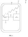
- FIG. 1 illustrates a block diagram of a communication device according to an exemplary embodiment of the disclosure.
- the communication device 100 can represent an all-in-one computer, a tablet computer, a mobile phone, a personal digital assistant (PDA), a satellite navigation device, video gaming device, a kiosk system in retail and tourist settings, a point of sale system, an automatic teller machine (ATM), an electronic accessory such as a smart watch, or any other suitable communication device that will be apparent to those skilled in the relevant art(s) without departing from the spirit and scope of the present disclosure.
- the communication device 100 can include a host processor 102, a communication module 104, and a touch-screen display 106 that are communicatively coupled via a communication interface 108.
- references in the disclosure to a "module” shall be understood to include at least one of software, firmware, and hardware (such as one or more circuits, microchips, or devices, or any combination thereof), and any combination thereof.
- each module can include one, or more than one, component within an actual device, and each component that forms a part of the described module can function either cooperatively or independently of any other component forming a part of the module.
- multiple modules described herein can represent a single component within an actual device. Further, components within a module can be in a single device or distributed among multiple devices in a wired or wireless manner.
- the host processor 102 controls overall operation and/or configuration of the communication device 100.
- the host processor 102 can receive and/or process information from a user interface such as an alphanumeric keypad, a microphone, a mouse, a speaker, and/or from other electrical devices or host devices that are coupled to the communication device 100.
- the host processor 102 can provide this information to the communication module 104 and/or the touch-screen display 106.
- the host processor 102 can receive and/or process information from the communication module 104 and/or the touch-screen display 106.
- the host processor 102 can provide this information to the communication module 104 and/or the touch-screen display 106 and/or to other electrical devices or host devices.
- the host processor 102 can execute one or more applications such as Short Message Service (SMS) for text messaging, electronic mailing, and/or audio and/or video recording to provide some examples, and/or software applications such as a calendar and/or a phone book to provide some examples.
- SMS Short Message Service
- the communication module 104 provides voice or data communication for a user of the communication device 100.
- the communication module 104 can include one or more of: a Bluetooth module, a Global Position System (GPS) module, a cellular module, a wireless local area network (WLAN) module, a near field communication (NFC) module, a radio frequency identification (RFID) module and/or a wireless power transfer (WPT) module.
- the Bluetooth module, the cellular module, the WLAN module, the NFC module, and the RFID module provide wireless communication between the communication device 100 and other Bluetooth, other cellular, other WLAN, other NFC, and other RFID enabled communication devices, respectively, in accordance with various communication standards or protocols.
- These various communication standards or protocols can include various cellular communication standards such as a third Generation Partnership Project (3GPP) Long Term Evolution (LTE) communication standard, a fourth generation (4G) mobile communication standard, or a third generation (3G) mobile communication standard, various networking protocols such a Wi-Fi communication standard, various NFC/RFID communication protocols such as ISO 1422, ISO/IEC 14443, ISO/IEC 15693, ISO/IEC 18000, or FeliCa to provide some examples.
- 3GPP Third Generation Partnership Project
- 4G fourth generation
- 3G third generation
- various networking protocols such as Wi-Fi communication standard
- various NFC/RFID communication protocols such as ISO 1422, ISO/IEC 14443, ISO/IEC 15693, ISO/IEC 18000, or FeliCa to provide some examples.
- the GPS module receives various signals from various satellites to determine location information for the communication device 100.
- the WPT module supports wireless transmission of power between the communication device 100 and another WPT enabled communication device.
- Each of the Bluetooth module, the cellular module, the WLAN module, the NFC module, and/or the RFID module can include a transmitter, a receiver, along with one or more processors, circuitry, and/or logic configured to transmit and/or receive wireless communications via one or more antennas.
- the transmitter and/or the receiver can include, but is not limited to, a digital signal processer (DSP), modulator and/or demodulator, a digital-to-analog converter (DAC), an analog-to-digital converter (ADC), and/or one or more frequency converters, such as one or more mixers, one or more local oscillators, and/or one or more filters to provide some examples.
- DSP digital signal processer
- DAC digital-to-analog converter
- ADC analog-to-digital converter
- frequency converters such as one or more mixers, one or more local oscillators, and/or one or more filters to provide some examples.
- the touch-screen display 106 provides a graphical user interface for the user of the communication device 100.
- the touch-screen display 106 operates as an output device to provide images relating to the voice or the data communication and/or the one or more applications to the user of the communication device 100.
- the touch-screen display 106 also operates as an input device to receive one or more commands and/or data from the user of the communication device 100 for the voice or data communication and/or the one or more applications.
- the communication interface 108 routes various communications between the host processor 102, the communication module 104, and the touch-screen display 106.
- the communication interface 108 can be implemented as a series of wired and/or wireless interconnections between the host processor 102, the communication module 104, and the touch-screen display 106.
- the interconnections of the communication interface 108 can be arranged to form a parallel interface to route communication between the host processor 102, the communication module 104, and the touch-screen display 106 in parallel, or a serial interface to route communication between the host processor 102, the communication module 104, and the touch-screen display 106, or any combination thereof.
- the host processor 102, the communication module 104, the touch-screen display 106, and the communication interface 108 are contained within, or supported by, a mechanical chassis 110 of the communication device 100.
- Consumers often desire to have the mechanical chassis 110 be completely fabricated using a conductive material, such as aluminum, copper, zinc, gold, tin, and/or silver to provide some examples, for its appearance and durability.
- the mechanical chassis 110 can interfere and/or distort communication signals traveling between the communication device 100 and other communication devices especially when magnetic fields are used for by these devices for communication and/or transferring power.
- FIG. 2 illustrates operation of a conventional communication device which utilizes magnetic fields for communication and/or transferring power.
- a conventional communication device 200 communicates with another communication device (not shown in FIG. 2 ) using a magnetic field 202.
- the magnetic field 202 can be used by the conventional communication device 200 to communicate information between the conventional communication device 200 and this other communication device.
- the conventional communication device 200 can communicate information to this other communication device by modulating the information onto the magnetic field 202 and can recover information from this other communication device by demodulating the magnetic field 202.
- the magnetic field 202 can be used by the conventional communication device 200 to derive and/or harvest power to permit its operation.
- the conventional communication device 200 can charge a charge storing element, such as a capacitor or a battery to provide some examples, using the magnetic field 202.
- the magnetic field 202 when the magnetic field 202 contacts, or is sufficiently proximate to, the conventional communication device 200, the magnetic field 202 induces one or more eddy currents 204 that flow in one or more closed loops around a surface of the conventional communication device 200.
- the one or more eddy currents 204 collectively generate a magnetic field 206 which can interfere and/or distort the magnetic field 202.
- the magnetic field 206 can destructively interfere with the magnetic field 202 which can result in a degradation of the magnetic field 202. This can diminish a capability of the conventional communication device 200 to communicate with another communication device and/or to derive and/or harvest power from the magnetic field 202.
- a communication device of the present disclosure such as the communication device 100 to provide an example, includes a mechanical chassis having one or more conductive regions separated by one or more non-conductive regions.
- the magnetic field When a magnetic field contacts, or is sufficiently proximate to, this communication device, the magnetic field induces one or more eddy currents that flow in one or more closed loops around a surface of the one or more conductive regions.
- the one or more non-conductive regions confine the one or more eddy currents to the one or more conductive regions.
- the magnetic fields generated by these one or more eddy currents are weaker than the magnetic field 206 as illustrated in FIG. 2 .
- FIG. 3 illustrates an exemplary mechanical chassis of the communication device according to an exemplary embodiment of the disclosure.
- a mechanical chassis 300 represents a frame or a housing containing or supporting electrical, mechanical, and/or electro-mechanical components of a communication device, such as the communication device 100 to provide an example.
- the mechanical chassis 300 includes a first enclosure 302 that is attached to a second enclosure 304.
- the mechanical chassis 300 can include one or more other mechanical bottom enclosures for attaching the first enclosure 302 and/or the second enclosure 304 thereto.
- the mechanical chassis 300 includes a bottom enclosure, represented as a first enclosure 302 in FIG. 3 , which is coupled to the second enclosure 304.
- the first enclosure 302 is attached to the second enclosure 304 to contain a touch-screen display 306, such as the touch-screen display 106 to provide an example, one or more semiconductor substrates and/or printed circuit boards 308, and a battery 210 of the communication device.
- the one or more semiconductor substrates and/or printed circuit boards 308 includes one or more semiconductor substrates and/or one or more printed circuit boards having a host processor, such as the host processor 102 to provide an example, and/or a communication module, such as the communication module 104 to provide an example, of the communication device.
- various other electrical, mechanical, and/or electro-mechanical components of the communication device can be contained within, or supported by, the first enclosure 302.
- the first enclosure 302 can include one or more openings for these other electrical, mechanical, and/or electro-mechanical components.
- the touch-screen display 306, the one or more semiconductor substrates and/or printed circuit boards 308, and/or these other electrical, mechanical, and/or electro-mechanical components of the communication device can be coupled together using one or more flexible flat cables (FFCs) though other couplings are possible that will be apparent to those skilled in the relevant art(s).
- FFCs flexible flat cables
- the first enclosure 302 includes one or more conductive regions separated by one or more non-conductive regions.
- the one or more conductive regions, as well as various other conductive regions described herein can be constructed of one or more elements, compounds, or alloys of one or more metals, such as aluminum, copper, zinc, gold, tin, and/or silver to provide some examples.
- the one or more non-conductive regions, as well as various other non-conductive regions described herein can be constructed of one or more synthetic or semi-synthetic organic compounds or materials, also referred to as plastic, to provide an example.
- any suitable material capable of conduction can be used for the one or more conductive regions and/or suitable material incapable, or relatively incapable, of conduction can be used for the one or more non-conductive regions which will be apparent to those skilled in the relevant art(s).
- a semi-conductive material can be used for either the one or more conductive regions and/or one or more non-conductive regions.
- the first enclosure 302 is formed using the one or more synthetic or semi-synthetic organic compounds or materials.
- the one or more synthetic or semi-synthetic organic compounds or materials are etched and filled with one or more elements, compounds, or alloys of one or more metals to form the one or more conductive regions.
- the one or more elements, compounds, or alloys of one or more metals used to form the one or more conductive regions can be formed onto the one or more synthetic or semi-synthetic organic compounds or materials and secured in place by applying a layer of natural or synthetic resin, such as epoxy resin to provide an example, onto the one or more synthetic or semi-synthetic organic compounds or materials to secure the one or more conductive regions to the one or more non-conductive regions.
- a layer of natural or synthetic resin such as epoxy resin to provide an example
- the one or more conductive regions can be implemented as one or more regular closed geometric structures, such as one or more regular polygons to provide an example, one or more irregular closed structures, such as one or more irregular polygons to provide an example, and/or any suitable combination of these closed structures that will be apparent to those skilled in the relevant art(s).
- the one or more conductive regions can be configured and arranged to form a tuned circuit. This tuned circuit can be optimally tuned to resonate at a frequency of a magnetic field. As such, the tuned circuit can amplify the magnetic field when the magnetic field contacts, or is sufficiently proximate to, the first enclosure 302.
- the one or more conductive regions and/or the one or more non-conductive regions can be of sufficient size and shape to give an appearance that the first enclosure 302 is constructed entirely of conductive material.
- the mechanical chassis 300 further includes a top enclosure, represented as the second enclosure 304 in FIG. 3 , which is coupled to the first enclosure 302.
- the second enclosure 304 is attached to the first enclosure 302 to contain the touch-screen display 306 and/or the one or more semiconductor substrates and/or printed circuit boards 308, a battery 310, the other electrical, mechanical, and/or electro-mechanical components of the communication device as well as the one or more flexible flat cables (FFCs) within the communication device.
- the second enclosure 304 can include one or more openings for the other electrical, mechanical, and/or electro-mechanical components, such as the digital camera, the input/output device, the microphone, and/or the speaker to provide some examples.
- the mechanical chassis 300 includes the first enclosure 302 and the second enclosure 304, this is for illustrative purposes only. Other configurations and arrangements for the mechanical chassis 300 are possible that will be apparent to those skilled in the relevant art(s).
- the first enclosure 302 and/or the second enclosure 304 can include multiple first bottom enclosures 302, and/or second bottom enclosures 304 having different sizes and/or shapes than as illustrated to form the foundation for assembling the electrical, the mechanical, and/or the electro-mechanical components of the communication device.
- the first enclosure 302 and/or the second enclosure 304 are formed into rectangular shapes as illustrated in FIG. 3 .
- first enclosure 302 and/or the second enclosure 304 may be formed into other geometric shapes without departing from the spirit and scope of the present disclosure. These other geometric shapes may include regular or irregular polygons and/or closed curves to provide some examples.
- the mechanical chassis 300 need not include the second enclosure 304.
- the touchscreen 306 is attached, or molded, to the first enclosure 302 using an appropriate adhesive or other attachment mechanism.
- the touchscreen 306 forms the top surface of the mechanical chassis 300, and the first enclosure 302 includes or forms the bottom surface of the mechanical chassis 300.
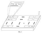
- FIG. 4 illustrates an exemplary bottom enclosure having one or more conductive regions separated by a non-conductive region according to an exemplary embodiment of the present disclosure.
- a bottom enclosure 400 includes conductive regions 402.1 through 402. n that are formed onto and/or within a non-conductive region 404.
- the bottom enclosure 400 can represent an exemplary embodiment of the first enclosure 302.
- the conductive regions 402.1 through 402. n are configured to be regular closed geometric structures, such as rectangles to provide an example.
- the conductive regions 402.1 through 402. n can be implemented using other regular closed geometric structures, one or more irregular closed structures, such as one or more irregular polygons to provide an example, and/or any suitable combination of closed structures that will be apparent to those skilled in the relevant art(s).
- the conductive regions 402 .1 through 402. n as illustrated in FIG. 4 have substantially similar dimensions, those skilled in the relevant art(s) will recognize that other dimensions, whether similar or dissimilar, are possible.
- the conductive regions 402.1 through 402. n are arranged in a series of rows and columns to form a matrix.
- the non-conductive region 404 separates the conductive regions 402.1 through 402. n in the matrix.
- the conductive regions 402.1 through 402. n are interdigitated with the non-conductive region 404.
- the separation between the conductive regions 402.1 through 402. n can be similar and/or dissimilar among pairs of the conductive regions 402.1 through 402. n .
- the separation between the conductive regions 402.1 through 402. n and the area of the conductive regions 402.1 through 402. n can be selectively chosen to form a capacitor.
- One or more of these capacitors can be configured and arranged to form a tuned circuit or a portion thereof.
- This tuned circuit can be optimally tuned to resonate at a frequency of a magnetic field.
- the tuned circuit can amplify a magnetic field when the magnetic field contacts, or is sufficiently proximate to, the bottom enclosure 400.
- the magnetic field when a magnetic field contacts, or is sufficiently proximate to, the bottom enclosure 400, the magnetic field induces one or more eddy currents 406 that flow in one or more closed loops around surfaces of the conductive regions 402.1 through 402. n .
- the non-conductive region 404 confines the one or more eddy currents 406 to the conductive regions 402.1 through 402. n .
- the magnetic fields generated by the one or more eddy currents 406 are weaker than a magnetic field generated by eddy currents in a bottom enclosure constructed entirely of conductive material.
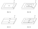
- a bottom enclosure 500 includes a conductive region 402.1 that is formed onto and/or within the non-conductive region 404 as illustrated in FIG. 5A .
- the conductive region 402.1 is centric to the bottom enclosure 500.
- the conductive region 402.1 can be non-centric to the bottom enclosure 500 without departing from the spirit and scope of the present disclosure.
- a bottom enclosure 502 includes conductive regions 402.1 through 402. n that are formed onto and/or within the non-conductive region 404 as illustrated in FIG. 5B . In this other example, the conductive regions 402.1 through 402.
- n are concentric to each other and separated from each other by the non-conductive region 404.
- a bottom enclosure 504 includes conductive regions 402.1 and 402.2 that are formed onto and/or within the non-conductive region 404 as illustrated in FIG. 5C .
- the conductive regions 402.1 and 402.2 are formed onto and/or within opposite sides of the bottom enclosure 504 and separated from each other by the non-conductive region 404.
- a bottom enclosure 506 includes conductive regions 402.1 and 402. n that are formed onto and/or within the non-conductive region 404 as illustrated in FIG. 5D .
- the conductive regions 402.1 and 402. n are arranged in a series of rows and separated from each other by the non-conductive region 404.
- Each of the bottom enclosures 500 through 506 can represent an exemplary embodiment of the first enclosure 302.
- FIG. 6 illustrates an exemplary bottom enclosure having a conductive region separated by one or more non-conductive regions according to an exemplary embodiment of the present disclosure.
- a bottom enclosure 600 includes non-conductive regions 602.1 through 602. k that that are formed onto and/or within a conductive region 604.
- the bottom enclosure 600 can represent an exemplary embodiment of the first enclosure 302.
- the non-conductive regions 602.1 through 602. k are configured to be regular closed geometric structures, such as rectangles to provide an example.
- the non-conductive regions 602.1 through 602. k can be implemented using other regular closed geometric structures, one or more irregular closed structures, such as one or more irregular polygons to provide an example, and/or any suitable combination of closed structures that will be apparent to those skilled in the relevant art(s).
- some of the non-conductive regions 602.1 through 602. k as illustrated in FIG. 6 have substantially similar dimensions, those skilled in the relevant art(s) will recognize that other dimensions, whether similar or dissimilar, are possible.
- the multiple non-conductive regions 602.1 through 602.k are arranged throughout the bottom enclosure 600 to separate the conductive region 604 into multiple conductive sub-regions 604.1 through 604.r.
- the multiple conductive sub-regions 604.1 through 604.r are configured to be regular closed geometric structures, such as rectangles to provide an example.
- the multiple conductive sub-regions 604.1 through 604.r can be implemented using other regular closed geometric structures, one or more irregular closed structures, such as one or more irregular polygons to provide an example, and/or any suitable combination of closed structures that will be apparent to those skilled in the relevant art(s).
- the multiple conductive sub-regions 604.1 through 604.r can be similar and/or dissimilar to one another.
- the magnetic field when a magnetic field contacts, or is sufficiently proximate to, the bottom enclosure 600, the magnetic field induces one or more eddy currents 606.1 through 606.r that flow in one or more closed loops around surfaces of the sub-regions 604.1 through 604.r.
- the non-conductive regions 602.1 through 602. k confine the one or more eddy currents 606.1 through 606.r to their respective multiple conductive sub-regions 604.1 through 604.r.
- the magnetic fields generated by the one or more eddy currents 606.1 through 606. r are weaker than a magnetic field generated by eddy currents in a bottom enclosure constructed entirely of conductive material.
- FIG. 7A illustrates an exemplary bottom enclosure having a first group of conductive regions adjacent to a second group of conductive regions according to an exemplary embodiment of the present disclosure.
- a bottom enclosure 700 includes a first group of conductive regions 702.1 through 702. n that are adjacent to a second group of conductive regions 704.1 through 704. m that are formed onto and/or within a base enclosure 706.
- the base enclosure 706 can be constructed of one or more elements, compounds, or alloys of one or more metals, such as aluminum, copper, zinc, gold, tin, and/or silver to provide some examples, one or more synthetic or semi-synthetic organic compounds or materials, also referred to as plastic, and/or any combination thereof to provide some examples.
- the bottom enclosure 700 can represent an exemplary embodiment of the first enclosure 302.
- the first group of conductive regions 702.1 through 702. n and the second group of conductive regions 704.1 through 704. m are configured to be regular closed geometric structures, such as rectangles to provide an example. However, the first group of conductive regions 702.1 through 702. n and the second group of conductive regions 704.1 through 704. m can be implemented using other regular closed geometric structures, one or more irregular closed structures, such as one or more irregular polygons to provide an example, and/or any suitable combination of closed structures that will be apparent to those skilled in the relevant art(s). Although the first group of conductive regions 702.1 through 702. n and the second group of conductive regions 704.1 through 704. m as illustrated in FIG. 7A have substantially similar dimensions, those skilled in the relevant art(s) will recognize that other dimensions, whether similar or dissimilar, are possible.
- the first group of conductive regions 702.1 through 702. n and the second group of conductive regions 704.1 through 704. m are arranged in a series of rows and columns to form a matrix.
- this example is not limiting, those skilled in the relevant art(s) will recognize that other arrangements for the first group of conductive regions 702.1 through 702. n and the second group of conductive regions 704.1 through 704. m are possible without departing from the spirit and scope of the present disclosure.
- FIG. 7B further illustrates the exemplary bottom enclosure according to an exemplary embodiment of the present disclosure.
- the line A-A traverses through a first row of the first group of conductive regions 702.1 through 702. n and the second group of conductive regions 704.1 through 704. m .
- a height of the first group of conductive regions 702.1 through 702. k along the first row is greater than a height of the second group of conductive regions 704.1 through 704. j along the first row.
- the magnetic field When a magnetic field contacts, or is sufficiently proximate to, the bottom enclosure 700, the magnetic field induces one or more eddy currents that flow in one or more closed loops around surfaces of the first group of conductive regions 702.1 through 702. n .
- the difference in height between the first group of conductive regions 702.1 through 702. n and the second group of conductive regions 704.1 through 704. m confine the one or more eddy currents to first group of conductive regions 702.1 through 702. n .
- the magnetic fields generated by the one or more eddy currents are weaker than a magnetic field generated by eddy currents in a bottom enclosure constructed entirely of conductive material.
- FIG. 8 illustrates an exemplary bottom enclosure having an integrated antenna according to an exemplary embodiment of the present disclosure.
- a bottom enclosure 800 includes a first group of conductive regions 802.1 through 802. n that are adjacent to a second conductive region 804 that are formed onto and/or within a conductive region 806.
- the bottom enclosure 800 can represent an exemplary embodiment of the first enclosure 302.
- the first group of conductive regions 802.1 through 802. n are configured to be regular closed geometric structures, such as rectangles to provide an example. However, the first group of conductive regions 802.1 through 802. n can be implemented using other regular closed geometric structures, one or more irregular closed structures, such as one or more irregular polygons to provide an example, and/or any suitable combination of closed structures that will be apparent to those skilled in the relevant art(s). Although some of the first group of conductive regions 802.1 through 802. n as illustrated in FIG. 8 have substantially similar dimensions, those skilled in the relevant art(s) will recognize that other dimensions, whether similar or dissimilar, are possible.
- the first group of conductive regions 802.1 through 802. n can be configured and arranged to form an integrated antenna for a communication device, such as the communication device 100 to provide an example.
- this integrated antenna can be used to transmit and/or receive information via a magnetic field.
- the communication device when transmitting information, provides a modulated current through the first group of conductive regions 802.1 through 802. n to generate a magnetic field.
- another communication device when receiving information, another communication device generates a magnetic field to induce a modulated current through the first group of conductive regions 802.1 through 802. n .
- the first group of conductive regions 802.1 through 802. n can be used by the communication device to derive and/or harvest power.
- a transmitter device generates a magnetic field to induce a current through the first group of conductive regions 802.1 through 802. n .
- the communication device derives and/or harvests power from this current.
- the second conductive region 804 can be implemented using any of the techniques described above in FIG. 3 through FIG. 7B .
- the second conductive region 804 can be configured to be a regular closed geometric structure, such as a rectangle to provide an example.
- the second conductive region 804 can be implemented using other regular closed geometric structures, one or more irregular closed structures, such as one or more irregular polygons to provide an example, and/or any suitable combination of closed structures that will be apparent to those skilled in the relevant art(s).
- module shall be understood to include at least one of software, firmware, and hardware (such as one or more circuits, microchips, or devices, or any combination thereof), and any combination thereof.
- each module can include one, or more than one, component within an actual device, and each component that forms a part of the described module can function either cooperatively or independently of any other component forming a part of the module.
- multiple modules described herein can represent a single component within an actual device. Further, components within a module can be in a single device or distributed among multiple devices in a wired or wireless manner.
- the present disclosure describes a mechanical chassis having one or more conductive regions separated by one or more non-conductive regions.
- the magnetic field induces one or more eddy currents that flow in one or more closed loops around a surface of the one or more conductive regions.
- the one or more non-conductive regions confine the one or more eddy currents to the one or more conductive regions.
- the magnetic fields generated by these one or more eddy currents are weaker than a magnetic field generated by eddy currents in a communication device having a mechanical chassis constructed entirely of conductive material.
Landscapes
- Engineering & Computer Science (AREA)
- Computer Networks & Wireless Communication (AREA)
- Signal Processing (AREA)
- Health & Medical Sciences (AREA)
- Computing Systems (AREA)
- General Health & Medical Sciences (AREA)
- Medical Informatics (AREA)
- Telephone Set Structure (AREA)
- Shielding Devices Or Components To Electric Or Magnetic Fields (AREA)
- Near-Field Transmission Systems (AREA)
Abstract
Description
- The present application claims the benefit of
U.S. Provisional Patent Appl. No. 61/978,143, filed April 10, 2014 - The present disclosure generally relates to a communication device and including a mechanical chassis of the communication device.
- The continued improvement of semiconductor fabrication processes has allowed manufacturers and designers to create a smaller and a more powerful electronic device. This smaller and more powerful electronic device is being integrated with near field communication (NFC) technology to facilitate the use of this electronic device in conducting daily transactions. For example, instead of carrying numerous credit cards, the credit information provided by these credit cards can be loaded and stored onto an NFC enabled device to be used as needed. The NFC enabled device is simply tapped to a credit card terminal to relay the credit information to complete a transaction. As another example, a ticket writing system, such as those used in bus and train terminals, may simply write ticket fare information onto the NFC enabled device instead of providing a paper ticket to a passenger. The passenger simply taps the NFC enabled device to a reader to ride the bus or the train without using a traditional the paper ticket.
- Furthermore, this smaller and more powerful electronic device is being integrated with wireless power transfer (WPT) capabilities to allow this device to wirelessly charge its internal batteries from a wireless power source without the use of a wired connection. In near-field or non-radiative WPT techniques, power is transferred over short distances by magnetic fields using inductive coupling between coils of wire. These techniques rely on the use of a magnetic field generated by a transmitter device to induce a current in the electronic device. This effect occurs in the electromagnetic near field, with the electronic device in close proximity to the transmitter device.
- Embodiments of the disclosure are described with reference to the accompanying drawings. In the drawings, like reference numbers indicate identical or functionally similar elements. Additionally, the left most digit(s) of a reference number identifies the drawing in which the reference number first appears.
-
FIG. 1 illustrates a block diagram of a communication device according to an exemplary embodiment of the disclosure; -
FIG. 2 illustrates operation of a conventional communication device which utilizes magnetic fields for communication and/or transferring power; -
FIG. 3 illustrates an exemplary mechanical chassis of the communication device according to an exemplary embodiment of the disclosure; -
FIG. 4 illustrates a first exemplary bottom enclosure having one or more conductive regions separated by a non-conductive region according to an exemplary embodiment of the present disclosure; -
FIG. 5A illustrates a second exemplary bottom enclosure having one or more conductive regions separated by a non-conductive region according to an exemplary embodiment of the present disclosure; -
FIG. 5B illustrates a third exemplary bottom enclosure having one or more conductive regions separated by a non-conductive region according to an exemplary embodiment of the present disclosure; -
FIG. 5C illustrates a fourth exemplary bottom enclosure having one or more conductive regions separated by a non-conductive region according to an exemplary embodiment of the present disclosure; -
FIG. 5D illustrates a fifth exemplary bottom enclosure having one or more conductive regions separated by a non-conductive region according to an exemplary embodiment of the present disclosure; -
FIG. 6 illustrates an exemplary bottom enclosure having a conductive region separated by one or more non-conductive regions according to an exemplary embodiment of the present disclosure; -
FIG. 7A illustrates an exemplary bottom enclosure having a first group of conductive regions adjacent to a second group of conductive regions according to an exemplary embodiment of the present disclosure; -
FIG. 7B further illustrates the exemplary bottom enclosure according to an exemplary embodiment of the present disclosure; and -
FIG. 8 illustrates an exemplary bottom enclosure having an integrated antenna according to an exemplary embodiment of the present disclosure - A communication device of the present disclosure includes a mechanical chassis having one or more conductive regions separated by one or more non-conductive regions. When a magnetic field contacts, or is sufficiently proximate to, this communication device, the magnetic field induces one or more eddy currents that flow in one or more closed loops around a surface of the one or more conductive regions. The one or more non-conductive regions confine the one or more eddy currents to the one or more conductive regions. The magnetic fields generated by these one or more eddy currents are weaker than a magnetic field generated by eddy currents in a communication device having a mechanical chassis constructed entirely of conductive material.
-
FIG. 1 illustrates a block diagram of a communication device according to an exemplary embodiment of the disclosure. Thecommunication device 100 can represent an all-in-one computer, a tablet computer, a mobile phone, a personal digital assistant (PDA), a satellite navigation device, video gaming device, a kiosk system in retail and tourist settings, a point of sale system, an automatic teller machine (ATM), an electronic accessory such as a smart watch, or any other suitable communication device that will be apparent to those skilled in the relevant art(s) without departing from the spirit and scope of the present disclosure. As illustrated inFIG. 1 , thecommunication device 100 can include ahost processor 102, acommunication module 104, and a touch-screen display 106 that are communicatively coupled via acommunication interface 108. References in the disclosure to a "module" shall be understood to include at least one of software, firmware, and hardware (such as one or more circuits, microchips, or devices, or any combination thereof), and any combination thereof. In addition, it will be understood that each module can include one, or more than one, component within an actual device, and each component that forms a part of the described module can function either cooperatively or independently of any other component forming a part of the module. Conversely, multiple modules described herein can represent a single component within an actual device. Further, components within a module can be in a single device or distributed among multiple devices in a wired or wireless manner. - The
host processor 102 controls overall operation and/or configuration of thecommunication device 100. Thehost processor 102 can receive and/or process information from a user interface such as an alphanumeric keypad, a microphone, a mouse, a speaker, and/or from other electrical devices or host devices that are coupled to thecommunication device 100. Thehost processor 102 can provide this information to thecommunication module 104 and/or the touch-screen display 106. Additionally, thehost processor 102 can receive and/or process information from thecommunication module 104 and/or the touch-screen display 106. Thehost processor 102 can provide this information to thecommunication module 104 and/or the touch-screen display 106 and/or to other electrical devices or host devices. Further, thehost processor 102 can execute one or more applications such as Short Message Service (SMS) for text messaging, electronic mailing, and/or audio and/or video recording to provide some examples, and/or software applications such as a calendar and/or a phone book to provide some examples. - The
communication module 104 provides voice or data communication for a user of thecommunication device 100. Thecommunication module 104 can include one or more of: a Bluetooth module, a Global Position System (GPS) module, a cellular module, a wireless local area network (WLAN) module, a near field communication (NFC) module, a radio frequency identification (RFID) module and/or a wireless power transfer (WPT) module. The Bluetooth module, the cellular module, the WLAN module, the NFC module, and the RFID module provide wireless communication between thecommunication device 100 and other Bluetooth, other cellular, other WLAN, other NFC, and other RFID enabled communication devices, respectively, in accordance with various communication standards or protocols. These various communication standards or protocols can include various cellular communication standards such as a third Generation Partnership Project (3GPP) Long Term Evolution (LTE) communication standard, a fourth generation (4G) mobile communication standard, or a third generation (3G) mobile communication standard, various networking protocols such a Wi-Fi communication standard, various NFC/RFID communication protocols such as ISO 1422, ISO/IEC 14443, ISO/IEC 15693, ISO/IEC 18000, or FeliCa to provide some examples. The GPS module receives various signals from various satellites to determine location information for thecommunication device 100. The WPT module supports wireless transmission of power between thecommunication device 100 and another WPT enabled communication device. - Each of the Bluetooth module, the cellular module, the WLAN module, the NFC module, and/or the RFID module can include a transmitter, a receiver, along with one or more processors, circuitry, and/or logic configured to transmit and/or receive wireless communications via one or more antennas. Those skilled in the relevant art(s) will recognize that the transmitter and/or the receiver can include, but is not limited to, a digital signal processer (DSP), modulator and/or demodulator, a digital-to-analog converter (DAC), an analog-to-digital converter (ADC), and/or one or more frequency converters, such as one or more mixers, one or more local oscillators, and/or one or more filters to provide some examples.
- The touch-
screen display 106 provides a graphical user interface for the user of thecommunication device 100. The touch-screen display 106 operates as an output device to provide images relating to the voice or the data communication and/or the one or more applications to the user of thecommunication device 100. The touch-screen display 106 also operates as an input device to receive one or more commands and/or data from the user of thecommunication device 100 for the voice or data communication and/or the one or more applications. - The
communication interface 108 routes various communications between thehost processor 102, thecommunication module 104, and the touch-screen display 106. Thecommunication interface 108 can be implemented as a series of wired and/or wireless interconnections between thehost processor 102, thecommunication module 104, and the touch-screen display 106. The interconnections of thecommunication interface 108 can be arranged to form a parallel interface to route communication between thehost processor 102, thecommunication module 104, and the touch-screen display 106 in parallel, or a serial interface to route communication between thehost processor 102, thecommunication module 104, and the touch-screen display 106, or any combination thereof. - As further illustrated in
FIG. 1 , thehost processor 102, thecommunication module 104, the touch-screen display 106, and thecommunication interface 108 are contained within, or supported by, amechanical chassis 110 of thecommunication device 100. Consumers often desire to have themechanical chassis 110 be completely fabricated using a conductive material, such as aluminum, copper, zinc, gold, tin, and/or silver to provide some examples, for its appearance and durability. However, themechanical chassis 110 can interfere and/or distort communication signals traveling between thecommunication device 100 and other communication devices especially when magnetic fields are used for by these devices for communication and/or transferring power. -
FIG. 2 illustrates operation of a conventional communication device which utilizes magnetic fields for communication and/or transferring power. As illustrated inFIG. 2 , aconventional communication device 200 communicates with another communication device (not shown inFIG. 2 ) using amagnetic field 202. For example, themagnetic field 202 can be used by theconventional communication device 200 to communicate information between theconventional communication device 200 and this other communication device. In this example, theconventional communication device 200 can communicate information to this other communication device by modulating the information onto themagnetic field 202 and can recover information from this other communication device by demodulating themagnetic field 202. Additionally, themagnetic field 202 can be used by theconventional communication device 200 to derive and/or harvest power to permit its operation. For example, theconventional communication device 200 can charge a charge storing element, such as a capacitor or a battery to provide some examples, using themagnetic field 202. - As further illustrated in
FIG. 2 , when themagnetic field 202 contacts, or is sufficiently proximate to, theconventional communication device 200, themagnetic field 202 induces one ormore eddy currents 204 that flow in one or more closed loops around a surface of theconventional communication device 200. The one ormore eddy currents 204 collectively generate amagnetic field 206 which can interfere and/or distort themagnetic field 202. For example, themagnetic field 206 can destructively interfere with themagnetic field 202 which can result in a degradation of themagnetic field 202. This can diminish a capability of theconventional communication device 200 to communicate with another communication device and/or to derive and/or harvest power from themagnetic field 202. - A communication device of the present disclosure, such as the
communication device 100 to provide an example, includes a mechanical chassis having one or more conductive regions separated by one or more non-conductive regions. When a magnetic field contacts, or is sufficiently proximate to, this communication device, the magnetic field induces one or more eddy currents that flow in one or more closed loops around a surface of the one or more conductive regions. The one or more non-conductive regions confine the one or more eddy currents to the one or more conductive regions. The magnetic fields generated by these one or more eddy currents are weaker than themagnetic field 206 as illustrated inFIG. 2 . -
FIG. 3 illustrates an exemplary mechanical chassis of the communication device according to an exemplary embodiment of the disclosure. Amechanical chassis 300 represents a frame or a housing containing or supporting electrical, mechanical, and/or electro-mechanical components of a communication device, such as thecommunication device 100 to provide an example. Themechanical chassis 300 includes afirst enclosure 302 that is attached to asecond enclosure 304. However, those skilled in the relevant art(s) will recognize that other configurations and arrangements are possible without departing from the spirit and scope of the present disclosure. For example, themechanical chassis 300 can include one or more other mechanical bottom enclosures for attaching thefirst enclosure 302 and/or thesecond enclosure 304 thereto. - The
mechanical chassis 300 includes a bottom enclosure, represented as afirst enclosure 302 inFIG. 3 , which is coupled to thesecond enclosure 304. Thefirst enclosure 302 is attached to thesecond enclosure 304 to contain a touch-screen display 306, such as the touch-screen display 106 to provide an example, one or more semiconductor substrates and/or printedcircuit boards 308, and a battery 210 of the communication device. In an exemplary embodiment, the one or more semiconductor substrates and/or printedcircuit boards 308 includes one or more semiconductor substrates and/or one or more printed circuit boards having a host processor, such as thehost processor 102 to provide an example, and/or a communication module, such as thecommunication module 104 to provide an example, of the communication device. In some situations, various other electrical, mechanical, and/or electro-mechanical components of the communication device, such as a digital camera, an input/output device, a microphone, and/or a speaker to provide some examples, can be contained within, or supported by, thefirst enclosure 302. Although not illustrated inFIG. 3 , thefirst enclosure 302 can include one or more openings for these other electrical, mechanical, and/or electro-mechanical components. Often times, the touch-screen display 306, the one or more semiconductor substrates and/or printedcircuit boards 308, and/or these other electrical, mechanical, and/or electro-mechanical components of the communication device can be coupled together using one or more flexible flat cables (FFCs) though other couplings are possible that will be apparent to those skilled in the relevant art(s). - The
first enclosure 302 includes one or more conductive regions separated by one or more non-conductive regions. The one or more conductive regions, as well as various other conductive regions described herein, can be constructed of one or more elements, compounds, or alloys of one or more metals, such as aluminum, copper, zinc, gold, tin, and/or silver to provide some examples. The one or more non-conductive regions, as well as various other non-conductive regions described herein, can be constructed of one or more synthetic or semi-synthetic organic compounds or materials, also referred to as plastic, to provide an example. However, any suitable material capable of conduction can be used for the one or more conductive regions and/or suitable material incapable, or relatively incapable, of conduction can be used for the one or more non-conductive regions which will be apparent to those skilled in the relevant art(s). In some situations, a semi-conductive material can be used for either the one or more conductive regions and/or one or more non-conductive regions. In an exemplary embodiment, thefirst enclosure 302 is formed using the one or more synthetic or semi-synthetic organic compounds or materials. In this exemplary embodiment, the one or more synthetic or semi-synthetic organic compounds or materials are etched and filled with one or more elements, compounds, or alloys of one or more metals to form the one or more conductive regions. Alternatively, the one or more elements, compounds, or alloys of one or more metals used to form the one or more conductive regions can be formed onto the one or more synthetic or semi-synthetic organic compounds or materials and secured in place by applying a layer of natural or synthetic resin, such as epoxy resin to provide an example, onto the one or more synthetic or semi-synthetic organic compounds or materials to secure the one or more conductive regions to the one or more non-conductive regions. - The one or more conductive regions can be implemented as one or more regular closed geometric structures, such as one or more regular polygons to provide an example, one or more irregular closed structures, such as one or more irregular polygons to provide an example, and/or any suitable combination of these closed structures that will be apparent to those skilled in the relevant art(s). In an exemplary embodiment, the one or more conductive regions can be configured and arranged to form a tuned circuit. This tuned circuit can be optimally tuned to resonate at a frequency of a magnetic field. As such, the tuned circuit can amplify the magnetic field when the magnetic field contacts, or is sufficiently proximate to, the
first enclosure 302. In another exemplary embodiment, the one or more conductive regions and/or the one or more non-conductive regions can be of sufficient size and shape to give an appearance that thefirst enclosure 302 is constructed entirely of conductive material. - The
mechanical chassis 300 further includes a top enclosure, represented as thesecond enclosure 304 inFIG. 3 , which is coupled to thefirst enclosure 302. Thesecond enclosure 304 is attached to thefirst enclosure 302 to contain the touch-screen display 306 and/or the one or more semiconductor substrates and/or printedcircuit boards 308, abattery 310, the other electrical, mechanical, and/or electro-mechanical components of the communication device as well as the one or more flexible flat cables (FFCs) within the communication device. Although not illustrated inFIG. 3 , thesecond enclosure 304 can include one or more openings for the other electrical, mechanical, and/or electro-mechanical components, such as the digital camera, the input/output device, the microphone, and/or the speaker to provide some examples. - Although the
mechanical chassis 300 includes thefirst enclosure 302 and thesecond enclosure 304, this is for illustrative purposes only. Other configurations and arrangements for themechanical chassis 300 are possible that will be apparent to those skilled in the relevant art(s). For example, thefirst enclosure 302 and/or thesecond enclosure 304 can include multiple firstbottom enclosures 302, and/or secondbottom enclosures 304 having different sizes and/or shapes than as illustrated to form the foundation for assembling the electrical, the mechanical, and/or the electro-mechanical components of the communication device. As another example, thefirst enclosure 302 and/or thesecond enclosure 304 are formed into rectangular shapes as illustrated inFIG. 3 . However, those skilled in the relevant art(s) will recognize thefirst enclosure 302 and/or thesecond enclosure 304 may be formed into other geometric shapes without departing from the spirit and scope of the present disclosure. These other geometric shapes may include regular or irregular polygons and/or closed curves to provide some examples. - Still further, in another embodiment, the
mechanical chassis 300 need not include thesecond enclosure 304. In this embodiment, thetouchscreen 306 is attached, or molded, to thefirst enclosure 302 using an appropriate adhesive or other attachment mechanism. In this embodiment, thetouchscreen 306 forms the top surface of themechanical chassis 300, and thefirst enclosure 302 includes or forms the bottom surface of themechanical chassis 300. -
FIG. 4 illustrates an exemplary bottom enclosure having one or more conductive regions separated by a non-conductive region according to an exemplary embodiment of the present disclosure. As illustrated inFIG. 4 , abottom enclosure 400 includes conductive regions 402.1 through 402.n that are formed onto and/or within anon-conductive region 404. Thebottom enclosure 400 can represent an exemplary embodiment of thefirst enclosure 302. - As illustrated in
FIG. 4 , the conductive regions 402.1 through 402.n are configured to be regular closed geometric structures, such as rectangles to provide an example. However, the conductive regions 402.1 through 402.n can be implemented using other regular closed geometric structures, one or more irregular closed structures, such as one or more irregular polygons to provide an example, and/or any suitable combination of closed structures that will be apparent to those skilled in the relevant art(s). Although the conductive regions 402 .1 through 402.n as illustrated inFIG. 4 have substantially similar dimensions, those skilled in the relevant art(s) will recognize that other dimensions, whether similar or dissimilar, are possible. - As additionally illustrated in
FIG. 4 , the conductive regions 402.1 through 402.n are arranged in a series of rows and columns to form a matrix. Thenon-conductive region 404 separates the conductive regions 402.1 through 402.n in the matrix. In an exemplary embodiment, the conductive regions 402.1 through 402.n are interdigitated with thenon-conductive region 404. The separation between the conductive regions 402.1 through 402.n can be similar and/or dissimilar among pairs of the conductive regions 402.1 through 402.n. In another exemplary embodiment, the separation between the conductive regions 402.1 through 402.n and the area of the conductive regions 402.1 through 402.n can be selectively chosen to form a capacitor. One or more of these capacitors can be configured and arranged to form a tuned circuit or a portion thereof. This tuned circuit can be optimally tuned to resonate at a frequency of a magnetic field. As such, the tuned circuit can amplify a magnetic field when the magnetic field contacts, or is sufficiently proximate to, thebottom enclosure 400. - As further illustrated in
FIG. 4 , when a magnetic field contacts, or is sufficiently proximate to, thebottom enclosure 400, the magnetic field induces one ormore eddy currents 406 that flow in one or more closed loops around surfaces of the conductive regions 402.1 through 402.n. Thenon-conductive region 404 confines the one ormore eddy currents 406 to the conductive regions 402.1 through 402.n. The magnetic fields generated by the one ormore eddy currents 406 are weaker than a magnetic field generated by eddy currents in a bottom enclosure constructed entirely of conductive material. - Those skilled in the relevant art(s) will recognize that other configurations and arrangements of conductive regions and/or non-conductive regions are possible. For example, a
bottom enclosure 500 includes a conductive region 402.1 that is formed onto and/or within thenon-conductive region 404 as illustrated inFIG. 5A . In this example, the conductive region 402.1 is centric to thebottom enclosure 500. However, those skilled in the relevant arts will recognize that the conductive region 402.1 can be non-centric to thebottom enclosure 500 without departing from the spirit and scope of the present disclosure. As another example, abottom enclosure 502 includes conductive regions 402.1 through 402.n that are formed onto and/or within thenon-conductive region 404 as illustrated inFIG. 5B . In this other example, the conductive regions 402.1 through 402.n are concentric to each other and separated from each other by thenon-conductive region 404. As a further example, abottom enclosure 504 includes conductive regions 402.1 and 402.2 that are formed onto and/or within thenon-conductive region 404 as illustrated inFIG. 5C . In this further example, the conductive regions 402.1 and 402.2 are formed onto and/or within opposite sides of thebottom enclosure 504 and separated from each other by thenon-conductive region 404. As a yet further example, abottom enclosure 506 includes conductive regions 402.1 and 402.n that are formed onto and/or within thenon-conductive region 404 as illustrated inFIG. 5D . In this yet further example, the conductive regions 402.1 and 402.n are arranged in a series of rows and separated from each other by thenon-conductive region 404. Each of thebottom enclosures 500 through 506 can represent an exemplary embodiment of thefirst enclosure 302. -
FIG. 6 illustrates an exemplary bottom enclosure having a conductive region separated by one or more non-conductive regions according to an exemplary embodiment of the present disclosure. As illustrated inFIG. 6 , abottom enclosure 600 includes non-conductive regions 602.1 through 602.k that that are formed onto and/or within aconductive region 604. Thebottom enclosure 600 can represent an exemplary embodiment of thefirst enclosure 302. - As illustrated in
FIG. 6 , the non-conductive regions 602.1 through 602.k are configured to be regular closed geometric structures, such as rectangles to provide an example. However, the non-conductive regions 602.1 through 602.k can be implemented using other regular closed geometric structures, one or more irregular closed structures, such as one or more irregular polygons to provide an example, and/or any suitable combination of closed structures that will be apparent to those skilled in the relevant art(s). Although some of the non-conductive regions 602.1 through 602.k as illustrated inFIG. 6 have substantially similar dimensions, those skilled in the relevant art(s) will recognize that other dimensions, whether similar or dissimilar, are possible. - As additionally illustrated in
FIG. 6 , the multiple non-conductive regions 602.1 through 602.k are arranged throughout thebottom enclosure 600 to separate theconductive region 604 into multiple conductive sub-regions 604.1 through 604.r. The multiple conductive sub-regions 604.1 through 604.r are configured to be regular closed geometric structures, such as rectangles to provide an example. However, the multiple conductive sub-regions 604.1 through 604.r can be implemented using other regular closed geometric structures, one or more irregular closed structures, such as one or more irregular polygons to provide an example, and/or any suitable combination of closed structures that will be apparent to those skilled in the relevant art(s). Additionally, the multiple conductive sub-regions 604.1 through 604.r can be similar and/or dissimilar to one another. - As further illustrated in
FIG. 6 , when a magnetic field contacts, or is sufficiently proximate to, thebottom enclosure 600, the magnetic field induces one or more eddy currents 606.1 through 606.r that flow in one or more closed loops around surfaces of the sub-regions 604.1 through 604.r. The non-conductive regions 602.1 through 602.k confine the one or more eddy currents 606.1 through 606.r to their respective multiple conductive sub-regions 604.1 through 604.r. The magnetic fields generated by the one or more eddy currents 606.1 through 606.r are weaker than a magnetic field generated by eddy currents in a bottom enclosure constructed entirely of conductive material. -
FIG. 7A illustrates an exemplary bottom enclosure having a first group of conductive regions adjacent to a second group of conductive regions according to an exemplary embodiment of the present disclosure. As illustrated inFIG. 7A , abottom enclosure 700 includes a first group of conductive regions 702.1 through 702.n that are adjacent to a second group of conductive regions 704.1 through 704.m that are formed onto and/or within abase enclosure 706. Thebase enclosure 706 can be constructed of one or more elements, compounds, or alloys of one or more metals, such as aluminum, copper, zinc, gold, tin, and/or silver to provide some examples, one or more synthetic or semi-synthetic organic compounds or materials, also referred to as plastic, and/or any combination thereof to provide some examples. Thebottom enclosure 700 can represent an exemplary embodiment of thefirst enclosure 302. - The first group of conductive regions 702.1 through 702.n and the second group of conductive regions 704.1 through 704.m are configured to be regular closed geometric structures, such as rectangles to provide an example. However, the first group of conductive regions 702.1 through 702.n and the second group of conductive regions 704.1 through 704.m can be implemented using other regular closed geometric structures, one or more irregular closed structures, such as one or more irregular polygons to provide an example, and/or any suitable combination of closed structures that will be apparent to those skilled in the relevant art(s). Although the first group of conductive regions 702.1 through 702.n and the second group of conductive regions 704.1 through 704.m as illustrated in
FIG. 7A have substantially similar dimensions, those skilled in the relevant art(s) will recognize that other dimensions, whether similar or dissimilar, are possible. - As additionally illustrated in
FIG. 7A , the first group of conductive regions 702.1 through 702.n and the second group of conductive regions 704.1 through 704.m are arranged in a series of rows and columns to form a matrix. However, this example is not limiting, those skilled in the relevant art(s) will recognize that other arrangements for the first group of conductive regions 702.1 through 702.n and the second group of conductive regions 704.1 through 704.m are possible without departing from the spirit and scope of the present disclosure. -
FIG. 7B further illustrates the exemplary bottom enclosure according to an exemplary embodiment of the present disclosure. As illustrated inFIG. 7A , the line A-A traverses through a first row of the first group of conductive regions 702.1 through 702.n and the second group of conductive regions 704.1 through 704.m. As illustrated inFIG. 7B , a height of the first group of conductive regions 702.1 through 702.k along the first row is greater than a height of the second group of conductive regions 704.1 through 704.j along the first row. - When a magnetic field contacts, or is sufficiently proximate to, the
bottom enclosure 700, the magnetic field induces one or more eddy currents that flow in one or more closed loops around surfaces of the first group of conductive regions 702.1 through 702.n. The difference in height between the first group of conductive regions 702.1 through 702.n and the second group of conductive regions 704.1 through 704.m confine the one or more eddy currents to first group of conductive regions 702.1 through 702.n. The magnetic fields generated by the one or more eddy currents are weaker than a magnetic field generated by eddy currents in a bottom enclosure constructed entirely of conductive material. -
FIG. 8 illustrates an exemplary bottom enclosure having an integrated antenna according to an exemplary embodiment of the present disclosure. As illustrated inFIG. 8 , abottom enclosure 800 includes a first group of conductive regions 802.1 through 802.n that are adjacent to a secondconductive region 804 that are formed onto and/or within aconductive region 806. Thebottom enclosure 800 can represent an exemplary embodiment of thefirst enclosure 302. - The first group of conductive regions 802.1 through 802.n are configured to be regular closed geometric structures, such as rectangles to provide an example. However, the first group of conductive regions 802.1 through 802.n can be implemented using other regular closed geometric structures, one or more irregular closed structures, such as one or more irregular polygons to provide an example, and/or any suitable combination of closed structures that will be apparent to those skilled in the relevant art(s). Although some of the first group of conductive regions 802.1 through 802.n as illustrated in
FIG. 8 have substantially similar dimensions, those skilled in the relevant art(s) will recognize that other dimensions, whether similar or dissimilar, are possible. - The first group of conductive regions 802.1 through 802.n can be configured and arranged to form an integrated antenna for a communication device, such as the
communication device 100 to provide an example. In an exemplary embodiment, this integrated antenna can be used to transmit and/or receive information via a magnetic field. For example, when transmitting information, the communication device provides a modulated current through the first group of conductive regions 802.1 through 802.n to generate a magnetic field. As another example, when receiving information, another communication device generates a magnetic field to induce a modulated current through the first group of conductive regions 802.1 through 802.n. In another exemplary embodiment, the first group of conductive regions 802.1 through 802.n can be used by the communication device to derive and/or harvest power. For example, a transmitter device generates a magnetic field to induce a current through the first group of conductive regions 802.1 through 802.n. In this example, the communication device derives and/or harvests power from this current. - The second
conductive region 804 can be implemented using any of the techniques described above inFIG. 3 through FIG. 7B . The secondconductive region 804 can be configured to be a regular closed geometric structure, such as a rectangle to provide an example. However, the secondconductive region 804 can be implemented using other regular closed geometric structures, one or more irregular closed structures, such as one or more irregular polygons to provide an example, and/or any suitable combination of closed structures that will be apparent to those skilled in the relevant art(s). - The following Detailed Description referred to accompanying figures to illustrate exemplary embodiments consistent with the disclosure. References in the disclosure to "an exemplary embodiment" indicates that the exemplary embodiment described can include a particular feature, structure, or characteristic, but every exemplary embodiment can not necessarily include the particular feature, structure, or characteristic. Moreover, such phrases are not necessarily referring to the same exemplary embodiment. Further, any feature, structure, or characteristic described in connection with an exemplary embodiment can be included, independently or in any combination, with features, structures, or characteristics of other exemplary embodiments whether or not explicitly described.
- The exemplary embodiments described within the disclosure have been provided for illustrative purposes, and are not intend to be limiting. Other exemplary embodiments are possible, and modifications can be made to the exemplary embodiments while remaining within the spirit and scope of the disclosure. The disclosure has been described with the aid of functional building blocks illustrating the implementation of specified functions and relationships thereof. The boundaries of these functional building blocks have been arbitrarily defined herein for the convenience of the description. Alternate boundaries can be defined so long as the specified functions and relationships thereof are appropriately performed.
- For purposes of this discussion, the term "module" shall be understood to include at least one of software, firmware, and hardware (such as one or more circuits, microchips, or devices, or any combination thereof), and any combination thereof. In addition, it will be understood that each module can include one, or more than one, component within an actual device, and each component that forms a part of the described module can function either cooperatively or independently of any other component forming a part of the module. Conversely, multiple modules described herein can represent a single component within an actual device. Further, components within a module can be in a single device or distributed among multiple devices in a wired or wireless manner.
- The Detailed Description of the exemplary embodiments fully revealed the general nature of the disclosure that others can, by applying knowledge of those skilled in relevant art(s), readily modify and/or adapt for various applications such exemplary embodiments, without undue experimentation, without departing from the spirit and scope of the disclosure. Therefore, such adaptations and modifications are intended to be within the meaning and plurality of equivalents of the exemplary embodiments based upon the teaching and guidance presented herein. It is to be understood that the phraseology or terminology herein is for the purpose of description and not of limitation, such that the terminology or phraseology of the present specification is to be interpreted by those skilled in relevant art(s) in light of the teachings herein.
- The present disclosure describes a mechanical chassis having one or more conductive regions separated by one or more non-conductive regions. When a magnetic field contacts, or is sufficiently proximate to, this communication device, the magnetic field induces one or more eddy currents that flow in one or more closed loops around a surface of the one or more conductive regions. The one or more non-conductive regions confine the one or more eddy currents to the one or more conductive regions. The magnetic fields generated by these one or more eddy currents are weaker than a magnetic field generated by eddy currents in a communication device having a mechanical chassis constructed entirely of conductive material.
Claims (20)
- A mechanical bottom enclosure for a communication device, the mechanical bottom enclosure comprising:a non-conductive region; anda plurality of conductive regions formed within or onto the non-conductive region, the plurality of conductive regions being arranged in a series of rows and columns to form a matrix,wherein the non-conductive region is configured to separate adjacent conductive regions from among the plurality of conductive regions.
- The mechanical bottom enclosure of claim 1, wherein each of the plurality of conductive regions is a regular closed geometric structure.
- The mechanical bottom enclosure of claim 2, wherein the regular closed geometric structure is a rectangle.
- The mechanical bottom enclosure of claim 1, wherein a first conductive region from among the plurality of conductive regions is separated from a second conductive region from among the plurality of conductive regions by a distance, and
wherein the distance is selectively chosen such that the first conductive region and the second conductive region form a capacitor of a tuned circuit. - The mechanical bottom enclosure of claim 4, wherein the tuned circuit is configured to resonate at a frequency of a magnetic field that is used for near field communication (NFC) or wireless power transfer (WPT).
- The mechanical bottom enclosure of claim 1, wherein the plurality of conductive regions comprises:one or more elements, compounds, or alloys of one or more metals.
- The mechanical bottom enclosure of claim 1, wherein the non-conductive region comprises:one or more synthetic or semi-synthetic organic compounds or materials.
- The mechanical bottom enclosure of claim 1, wherein the plurality of conductive regions is formed onto the non-conductive region, and further comprising:a layer of natural or synthetic resin, formed onto the plurality of conductive regions and the non-conductive region, configured to secure the plurality of conductive regions to the non-conductive region.
- The mechanical bottom enclosure of claim 1, wherein the mechanical bottom enclosure is configured to be attached to a mechanical top enclosure, the mechanical bottom enclosure and the mechanical top enclosure being configured to contain electrical, mechanical, and/or electro-mechanical components of the communication device.
- A communication device, comprising:a touch-screen display;one or more semiconductor substrates and/or printed circuit boards having a near field communication (NFC) module or a wireless power transfer (WPT) module; anda mechanical chassis having a top enclosure and a bottom enclosure, the top enclosure and the bottom enclosure being configured to contain the touch-screen display and the one or more semiconductor substrates and/or printed circuit boards,wherein the bottom enclosure comprises:a non-conductive region; anda plurality of conductive regions, andwherein a first conductive region from among the plurality of conductive regions is separated from a second conductive region from among the plurality of conductive regions to form a capacitor of a tuned circuit, the tuned circuit being configured to resonate at a frequency of a magnetic field that is used by the NFC module or the WPT module.
- The communication device of claim 10, wherein the non-conductive region is configured to confine a plurality of eddy currents induced by the magnetic field to the plurality of conductive regions.
- The communication device of claim 10, wherein the plurality of conductive regions is arranged in a series of rows and columns to form a matrix, and
wherein the non-conductive region is configured to separate adjacent conductive regions from among the plurality of conductive regions - The communication device of claim 10, wherein the first conductive region is configured to be concentric to the second conductive region and to be separated from the second conductive region by the non-conductive region.
- The communication device of claim 10, wherein the plurality of conductive regions is arranged in a series of rows, each of the series of rows being separated from each other by the non-conductive region.
- The communication device of claim 10, wherein a first group of conductive regions from among the plurality of conductive regions is configured to be used as an antenna by the NFC module or the WPT module.
- The communication device of claim 15, wherein a second group of conductive regions from among the plurality of conductive regions comprises:the first conductive region and the second conductive region.
- A mechanical bottom enclosure for a communication device, the mechanical bottom enclosure comprising:a conductive region; anda plurality of non-conductive regions, formed within or onto the conductive region, configured to separate the conductive region into a plurality of conductive sub-regions,wherein the plurality of non-conductive regions are configured to confine a plurality of eddy currents to closed loops around surfaces of the plurality of conductive sub-regions.
- The mechanical bottom enclosure of claim 19, wherein the plurality of eddy currents is induced by a magnetic field contacting, or being sufficiently proximate to, the mechanical bottom enclosure.
- The mechanical bottom enclosure of claim 17, wherein each of the plurality of non-conductive regions is a regular closed geometric structure.
- The mechanical bottom enclosure of claim 19, wherein the regular closed geometric structure is a rectangle.
Applications Claiming Priority (2)
| Application Number | Priority Date | Filing Date | Title |
|---|---|---|---|
| US201461978143P | 2014-04-10 | 2014-04-10 | |
| US14/682,366 US9730002B2 (en) | 2014-04-10 | 2015-04-09 | Mechanical enclosures for a communication device |
Publications (3)
| Publication Number | Publication Date |
|---|---|
| EP2930855A1 true EP2930855A1 (en) | 2015-10-14 |
| EP2930855B1 EP2930855B1 (en) | 2018-12-19 |
| EP2930855B8 EP2930855B8 (en) | 2019-03-06 |
Family
ID=53264447
Family Applications (1)
| Application Number | Title | Priority Date | Filing Date |
|---|---|---|---|
| EP15163114.0A Active EP2930855B8 (en) | 2014-04-10 | 2015-04-10 | Mechanical enclosures for a communication device |
Country Status (4)
| Country | Link |
|---|---|
| US (1) | US9730002B2 (en) |
| EP (1) | EP2930855B8 (en) |
| CN (2) | CN104981123B (en) |
| HK (1) | HK1214464A1 (en) |
Families Citing this family (6)
| Publication number | Priority date | Publication date | Assignee | Title |
|---|---|---|---|---|
| US9730002B2 (en) * | 2014-04-10 | 2017-08-08 | Avago Technologies General Ip (Singapore) Pte. Ltd. | Mechanical enclosures for a communication device |
| US9788277B2 (en) * | 2015-01-15 | 2017-10-10 | Mediatek Inc. | Power saving mechanism for in-pocket detection |
| US10333334B2 (en) | 2016-01-29 | 2019-06-25 | Qualcomm Incorporated | Wireless power transfer in an electronic device having a tuned metallic body |
| CN105845756B (en) * | 2016-05-20 | 2017-07-14 | 浙江光隆能源科技股份有限公司 | Close main grid polycrystalline back of solar cell silver paste of grid four and preparation method thereof |
| USD939508S1 (en) * | 2018-11-19 | 2021-12-28 | Awb Company | Device performance enhancer |
| TWI725435B (en) | 2019-05-27 | 2021-04-21 | 緯創資通股份有限公司 | Electronic apparatus |
Citations (2)
| Publication number | Priority date | Publication date | Assignee | Title |
|---|---|---|---|---|
| WO2013103948A2 (en) * | 2012-01-08 | 2013-07-11 | Access Business Group International Llc | Wireless power transfer through conductive materials |
| US20130190052A1 (en) * | 2012-01-19 | 2013-07-25 | Motorola Mobility, Inc. | Managed material fabric for composite housing |
Family Cites Families (14)
| Publication number | Priority date | Publication date | Assignee | Title |
|---|---|---|---|---|
| US5360941A (en) * | 1991-10-28 | 1994-11-01 | Cubic Automatic Revenue Collection Group | Magnetically permeable electrostatic shield |
| FI105762B (en) * | 1997-11-21 | 2000-09-29 | Nokia Mobile Phones Ltd | Wireless communication means |
| US6853687B2 (en) * | 2000-01-12 | 2005-02-08 | Wherenet Corp | Proximity-based magnetic field generator for controlling operation of RF burst-transmitting tags of geolocation system |
| US6970160B2 (en) * | 2002-12-19 | 2005-11-29 | 3M Innovative Properties Company | Lattice touch-sensing system |
| KR100964189B1 (en) * | 2008-08-08 | 2010-06-17 | 한국전자통신연구원 | Magnetic field detection or transmission method using detachable magnetic resonator and apparatus therefor |
| US8214003B2 (en) * | 2009-03-13 | 2012-07-03 | Pong Research Corporation | RF radiation redirection away from portable communication device user |
| CN101800354B (en) * | 2008-11-06 | 2015-03-11 | 庞研究有限公司 | Antennas Embedded in Batteries, Wireless Devices, and Smart Cases for Wireless Devices |
| TW201036022A (en) * | 2009-03-30 | 2010-10-01 | O Din Product Design Studio | Improved electromagnetic sensing structure of a housing and method thereof |
| CA2752609C (en) * | 2010-09-21 | 2018-08-14 | Inside Secure | Nfc card for portable device |
| CN102984929B (en) * | 2011-09-07 | 2015-07-08 | 港易有限公司 | Radiation-proof laminate for electronic device and method for embedding the laminate in case |
| US9838060B2 (en) * | 2011-11-02 | 2017-12-05 | Antenna79, Inc. | Protective cover for a wireless device |
| US9728326B2 (en) * | 2013-10-22 | 2017-08-08 | Thales Visionix, Inc. | Apparatus for eddy current inhibiting electro-magnetic interference shielding |
| US9730002B2 (en) * | 2014-04-10 | 2017-08-08 | Avago Technologies General Ip (Singapore) Pte. Ltd. | Mechanical enclosures for a communication device |
| US20160111889A1 (en) * | 2014-10-20 | 2016-04-21 | Qualcomm Incorporated | Segmented conductive back cover for wireless power transfer |
-
2015
- 2015-04-09 US US14/682,366 patent/US9730002B2/en active Active
- 2015-04-10 EP EP15163114.0A patent/EP2930855B8/en active Active
- 2015-04-10 CN CN201510170637.XA patent/CN104981123B/en active Active
- 2015-04-10 CN CN201520217473.7U patent/CN204948543U/en not_active Expired - Fee Related
-
2016
- 2016-02-24 HK HK16102119.4A patent/HK1214464A1/en unknown
Patent Citations (2)
| Publication number | Priority date | Publication date | Assignee | Title |
|---|---|---|---|---|
| WO2013103948A2 (en) * | 2012-01-08 | 2013-07-11 | Access Business Group International Llc | Wireless power transfer through conductive materials |
| US20130190052A1 (en) * | 2012-01-19 | 2013-07-25 | Motorola Mobility, Inc. | Managed material fabric for composite housing |
Also Published As
| Publication number | Publication date |
|---|---|
| EP2930855B1 (en) | 2018-12-19 |
| CN104981123A (en) | 2015-10-14 |
| EP2930855B8 (en) | 2019-03-06 |
| HK1214464A1 (en) | 2016-07-22 |
| US9730002B2 (en) | 2017-08-08 |
| CN104981123B (en) | 2018-09-11 |
| CN204948543U (en) | 2016-01-06 |
| US20150296328A1 (en) | 2015-10-15 |
Similar Documents
| Publication | Publication Date | Title |
|---|---|---|
| US9730002B2 (en) | Mechanical enclosures for a communication device | |
| US10148321B2 (en) | Antenna for near field communication, accessory and electronic device including the same | |
| CN105809428B (en) | Electronic device and transaction method using the same | |
| US10014577B2 (en) | Aerial module and mobile terminal device | |
| EP3322028A1 (en) | Wireless antenna for wireless charging and nfc communication and wireless terminal to which same is applied | |
| CN107785648B (en) | Electronic device with loop antenna | |
| US20130248601A1 (en) | Mobile computer with integrated near field communication antenna | |
| CN106663873A (en) | NFC antenna module and portable terminal having same | |
| US9173247B2 (en) | Mobile wireless communications device including parallel NFC loop antennas and associated methods | |
| US20190027302A1 (en) | Shield Unit For Wireless Charging And Wireless Power Transmission Module Comprising Same | |
| US20170324147A1 (en) | Antenna module having metal frame antenna segment and electronic device including the same | |
| US20190235584A1 (en) | Electronic device | |
| US12581007B2 (en) | Electronic device including multiple PCBS and antennas printed on PCBS | |
| US20130194155A1 (en) | Wireless communication system, and small portable device, housing case for a small portable device, and communication device for a small portable device to be used in the wireless communication system | |
| KR102533402B1 (en) | Antenna for near filed communication, accessory and electronic apparatus including the same | |
| JPWO2005094046A1 (en) | Wireless communication system, fixed information device, portable terminal device | |
| US10476555B2 (en) | Chassis based antenna for a near field communication (NFC) enabled device | |
| EP2523359A1 (en) | Communications terminal device | |
| US20200006852A1 (en) | Booster antenna structure, communication apparatus, and case | |
| US20130176094A1 (en) | Antenna assembly and communication device having same | |
| CN215344569U (en) | NFC device and mobile terminal | |
| EP2621018B1 (en) | Mobile wireless communications device including parallel nfc loop antennas and associated methods | |
| JP3182247U (en) | Case for portable device | |
| JP2005348066A (en) | Antenna arrangement structure and communication terminal | |
| TWM404548U (en) | Mobile communication device with combining near field communication function |
Legal Events
| Date | Code | Title | Description |
|---|---|---|---|
| PUAI | Public reference made under article 153(3) epc to a published international application that has entered the european phase |
Free format text: ORIGINAL CODE: 0009012 |
|
| 17P | Request for examination filed |
Effective date: 20150410 |
|
| AK | Designated contracting states |
Kind code of ref document: A1 Designated state(s): AL AT BE BG CH CY CZ DE DK EE ES FI FR GB GR HR HU IE IS IT LI LT LU LV MC MK MT NL NO PL PT RO RS SE SI SK SM TR |
|
| AX | Request for extension of the european patent |
Extension state: BA ME |
|
| STAA | Information on the status of an ep patent application or granted ep patent |
Free format text: STATUS: REQUEST FOR EXAMINATION WAS MADE |
|
| R17P | Request for examination filed (corrected) |
Effective date: 20150410 |
|
| RAP1 | Party data changed (applicant data changed or rights of an application transferred) |
Owner name: AVAGO TECHNOLOGIES GENERAL IP (SINGAPORE) PTE. LTD |
|
| GRAP | Despatch of communication of intention to grant a patent |
Free format text: ORIGINAL CODE: EPIDOSNIGR1 |
|
| STAA | Information on the status of an ep patent application or granted ep patent |
Free format text: STATUS: GRANT OF PATENT IS INTENDED |
|
| INTG | Intention to grant announced |
Effective date: 20180709 |
|
| GRAS | Grant fee paid |
Free format text: ORIGINAL CODE: EPIDOSNIGR3 |
|
| GRAA | (expected) grant |
Free format text: ORIGINAL CODE: 0009210 |
|
| STAA | Information on the status of an ep patent application or granted ep patent |
Free format text: STATUS: THE PATENT HAS BEEN GRANTED |
|
| AK | Designated contracting states |
Kind code of ref document: B1 Designated state(s): AL AT BE BG CH CY CZ DE DK EE ES FI FR GB GR HR HU IE IS IT LI LT LU LV MC MK MT NL NO PL PT RO RS SE SI SK SM TR |
|
| REG | Reference to a national code |
Ref country code: GB Ref legal event code: FG4D |
|
| RAP2 | Party data changed (patent owner data changed or rights of a patent transferred) |
Owner name: AVAGO TECHNOLOGIES INTERNATIONAL SALES PTE. LIMITE |
|
| REG | Reference to a national code |
Ref country code: CH Ref legal event code: EP |
|
| REG | Reference to a national code |
Ref country code: IE Ref legal event code: FG4D |
|
| REG | Reference to a national code |
Ref country code: DE Ref legal event code: R096 Ref document number: 602015021748 Country of ref document: DE |
|
| REG | Reference to a national code |
Ref country code: AT Ref legal event code: REF Ref document number: 1079792 Country of ref document: AT Kind code of ref document: T Effective date: 20190115 |
|
| REG | Reference to a national code |
Ref country code: CH Ref legal event code: PK Free format text: BERICHTIGUNG B8 |
|
| REG | Reference to a national code |
Ref country code: NL Ref legal event code: FP |
|
| PG25 | Lapsed in a contracting state [announced via postgrant information from national office to epo] |
Ref country code: BG Free format text: LAPSE BECAUSE OF FAILURE TO SUBMIT A TRANSLATION OF THE DESCRIPTION OR TO PAY THE FEE WITHIN THE PRESCRIBED TIME-LIMIT Effective date: 20190319 Ref country code: LT Free format text: LAPSE BECAUSE OF FAILURE TO SUBMIT A TRANSLATION OF THE DESCRIPTION OR TO PAY THE FEE WITHIN THE PRESCRIBED TIME-LIMIT Effective date: 20181219 Ref country code: HR Free format text: LAPSE BECAUSE OF FAILURE TO SUBMIT A TRANSLATION OF THE DESCRIPTION OR TO PAY THE FEE WITHIN THE PRESCRIBED TIME-LIMIT Effective date: 20181219 Ref country code: LV Free format text: LAPSE BECAUSE OF FAILURE TO SUBMIT A TRANSLATION OF THE DESCRIPTION OR TO PAY THE FEE WITHIN THE PRESCRIBED TIME-LIMIT Effective date: 20181219 Ref country code: NO Free format text: LAPSE BECAUSE OF FAILURE TO SUBMIT A TRANSLATION OF THE DESCRIPTION OR TO PAY THE FEE WITHIN THE PRESCRIBED TIME-LIMIT Effective date: 20190319 Ref country code: FI Free format text: LAPSE BECAUSE OF FAILURE TO SUBMIT A TRANSLATION OF THE DESCRIPTION OR TO PAY THE FEE WITHIN THE PRESCRIBED TIME-LIMIT Effective date: 20181219 |
|
| REG | Reference to a national code |
Ref country code: LT Ref legal event code: MG4D |
|
| REG | Reference to a national code |
Ref country code: AT Ref legal event code: MK05 Ref document number: 1079792 Country of ref document: AT Kind code of ref document: T Effective date: 20181219 |
|
| PG25 | Lapsed in a contracting state [announced via postgrant information from national office to epo] |
Ref country code: AL Free format text: LAPSE BECAUSE OF FAILURE TO SUBMIT A TRANSLATION OF THE DESCRIPTION OR TO PAY THE FEE WITHIN THE PRESCRIBED TIME-LIMIT Effective date: 20181219 Ref country code: SE Free format text: LAPSE BECAUSE OF FAILURE TO SUBMIT A TRANSLATION OF THE DESCRIPTION OR TO PAY THE FEE WITHIN THE PRESCRIBED TIME-LIMIT Effective date: 20181219 Ref country code: RS Free format text: LAPSE BECAUSE OF FAILURE TO SUBMIT A TRANSLATION OF THE DESCRIPTION OR TO PAY THE FEE WITHIN THE PRESCRIBED TIME-LIMIT Effective date: 20181219 Ref country code: GR Free format text: LAPSE BECAUSE OF FAILURE TO SUBMIT A TRANSLATION OF THE DESCRIPTION OR TO PAY THE FEE WITHIN THE PRESCRIBED TIME-LIMIT Effective date: 20190320 |
|
| PG25 | Lapsed in a contracting state [announced via postgrant information from national office to epo] |
Ref country code: CZ Free format text: LAPSE BECAUSE OF FAILURE TO SUBMIT A TRANSLATION OF THE DESCRIPTION OR TO PAY THE FEE WITHIN THE PRESCRIBED TIME-LIMIT Effective date: 20181219 Ref country code: PT Free format text: LAPSE BECAUSE OF FAILURE TO SUBMIT A TRANSLATION OF THE DESCRIPTION OR TO PAY THE FEE WITHIN THE PRESCRIBED TIME-LIMIT Effective date: 20190419 Ref country code: IT Free format text: LAPSE BECAUSE OF FAILURE TO SUBMIT A TRANSLATION OF THE DESCRIPTION OR TO PAY THE FEE WITHIN THE PRESCRIBED TIME-LIMIT Effective date: 20181219 Ref country code: ES Free format text: LAPSE BECAUSE OF FAILURE TO SUBMIT A TRANSLATION OF THE DESCRIPTION OR TO PAY THE FEE WITHIN THE PRESCRIBED TIME-LIMIT Effective date: 20181219 Ref country code: PL Free format text: LAPSE BECAUSE OF FAILURE TO SUBMIT A TRANSLATION OF THE DESCRIPTION OR TO PAY THE FEE WITHIN THE PRESCRIBED TIME-LIMIT Effective date: 20181219 |
|
| PG25 | Lapsed in a contracting state [announced via postgrant information from national office to epo] |
Ref country code: SK Free format text: LAPSE BECAUSE OF FAILURE TO SUBMIT A TRANSLATION OF THE DESCRIPTION OR TO PAY THE FEE WITHIN THE PRESCRIBED TIME-LIMIT Effective date: 20181219 Ref country code: RO Free format text: LAPSE BECAUSE OF FAILURE TO SUBMIT A TRANSLATION OF THE DESCRIPTION OR TO PAY THE FEE WITHIN THE PRESCRIBED TIME-LIMIT Effective date: 20181219 Ref country code: IS Free format text: LAPSE BECAUSE OF FAILURE TO SUBMIT A TRANSLATION OF THE DESCRIPTION OR TO PAY THE FEE WITHIN THE PRESCRIBED TIME-LIMIT Effective date: 20190419 Ref country code: SM Free format text: LAPSE BECAUSE OF FAILURE TO SUBMIT A TRANSLATION OF THE DESCRIPTION OR TO PAY THE FEE WITHIN THE PRESCRIBED TIME-LIMIT Effective date: 20181219 Ref country code: EE Free format text: LAPSE BECAUSE OF FAILURE TO SUBMIT A TRANSLATION OF THE DESCRIPTION OR TO PAY THE FEE WITHIN THE PRESCRIBED TIME-LIMIT Effective date: 20181219 |
|
| REG | Reference to a national code |
Ref country code: DE Ref legal event code: R097 Ref document number: 602015021748 Country of ref document: DE |
|
| PLBE | No opposition filed within time limit |
Free format text: ORIGINAL CODE: 0009261 |
|
| STAA | Information on the status of an ep patent application or granted ep patent |
Free format text: STATUS: NO OPPOSITION FILED WITHIN TIME LIMIT |
|
| PG25 | Lapsed in a contracting state [announced via postgrant information from national office to epo] |
Ref country code: DK Free format text: LAPSE BECAUSE OF FAILURE TO SUBMIT A TRANSLATION OF THE DESCRIPTION OR TO PAY THE FEE WITHIN THE PRESCRIBED TIME-LIMIT Effective date: 20181219 Ref country code: AT Free format text: LAPSE BECAUSE OF FAILURE TO SUBMIT A TRANSLATION OF THE DESCRIPTION OR TO PAY THE FEE WITHIN THE PRESCRIBED TIME-LIMIT Effective date: 20181219 |
|
| 26N | No opposition filed |
Effective date: 20190920 |
|
| REG | Reference to a national code |
Ref country code: CH Ref legal event code: PL |
|
| REG | Reference to a national code |
Ref country code: BE Ref legal event code: MM Effective date: 20190430 |
|
| GBPC | Gb: european patent ceased through non-payment of renewal fee |
Effective date: 20190410 |
|
| PG25 | Lapsed in a contracting state [announced via postgrant information from national office to epo] |
Ref country code: LU Free format text: LAPSE BECAUSE OF NON-PAYMENT OF DUE FEES Effective date: 20190410 Ref country code: MC Free format text: LAPSE BECAUSE OF FAILURE TO SUBMIT A TRANSLATION OF THE DESCRIPTION OR TO PAY THE FEE WITHIN THE PRESCRIBED TIME-LIMIT Effective date: 20181219 |
|
| PG25 | Lapsed in a contracting state [announced via postgrant information from national office to epo] |
Ref country code: CH Free format text: LAPSE BECAUSE OF NON-PAYMENT OF DUE FEES Effective date: 20190430 Ref country code: GB Free format text: LAPSE BECAUSE OF NON-PAYMENT OF DUE FEES Effective date: 20190410 Ref country code: LI Free format text: LAPSE BECAUSE OF NON-PAYMENT OF DUE FEES Effective date: 20190430 |
|
| PG25 | Lapsed in a contracting state [announced via postgrant information from national office to epo] |
Ref country code: BE Free format text: LAPSE BECAUSE OF NON-PAYMENT OF DUE FEES Effective date: 20190430 Ref country code: SI Free format text: LAPSE BECAUSE OF FAILURE TO SUBMIT A TRANSLATION OF THE DESCRIPTION OR TO PAY THE FEE WITHIN THE PRESCRIBED TIME-LIMIT Effective date: 20181219 Ref country code: FR Free format text: LAPSE BECAUSE OF NON-PAYMENT OF DUE FEES Effective date: 20190430 |
|
| PG25 | Lapsed in a contracting state [announced via postgrant information from national office to epo] |
Ref country code: TR Free format text: LAPSE BECAUSE OF FAILURE TO SUBMIT A TRANSLATION OF THE DESCRIPTION OR TO PAY THE FEE WITHIN THE PRESCRIBED TIME-LIMIT Effective date: 20181219 |
|
| PG25 | Lapsed in a contracting state [announced via postgrant information from national office to epo] |
Ref country code: IE Free format text: LAPSE BECAUSE OF NON-PAYMENT OF DUE FEES Effective date: 20190410 |
|
| PG25 | Lapsed in a contracting state [announced via postgrant information from national office to epo] |
Ref country code: CY Free format text: LAPSE BECAUSE OF FAILURE TO SUBMIT A TRANSLATION OF THE DESCRIPTION OR TO PAY THE FEE WITHIN THE PRESCRIBED TIME-LIMIT Effective date: 20181219 |
|
| PG25 | Lapsed in a contracting state [announced via postgrant information from national office to epo] |
Ref country code: MT Free format text: LAPSE BECAUSE OF FAILURE TO SUBMIT A TRANSLATION OF THE DESCRIPTION OR TO PAY THE FEE WITHIN THE PRESCRIBED TIME-LIMIT Effective date: 20181219 Ref country code: HU Free format text: LAPSE BECAUSE OF FAILURE TO SUBMIT A TRANSLATION OF THE DESCRIPTION OR TO PAY THE FEE WITHIN THE PRESCRIBED TIME-LIMIT; INVALID AB INITIO Effective date: 20150410 |
|
| PG25 | Lapsed in a contracting state [announced via postgrant information from national office to epo] |
Ref country code: MK Free format text: LAPSE BECAUSE OF FAILURE TO SUBMIT A TRANSLATION OF THE DESCRIPTION OR TO PAY THE FEE WITHIN THE PRESCRIBED TIME-LIMIT Effective date: 20181219 |
|
| PGFP | Annual fee paid to national office [announced via postgrant information from national office to epo] |
Ref country code: NL Payment date: 20260319 Year of fee payment: 12 |
|
| PGFP | Annual fee paid to national office [announced via postgrant information from national office to epo] |
Ref country code: DE Payment date: 20260410 Year of fee payment: 12 |