EP2930790B1 - Array antenna - Google Patents
Array antenna Download PDFInfo
- Publication number
- EP2930790B1 EP2930790B1 EP15162366.7A EP15162366A EP2930790B1 EP 2930790 B1 EP2930790 B1 EP 2930790B1 EP 15162366 A EP15162366 A EP 15162366A EP 2930790 B1 EP2930790 B1 EP 2930790B1
- Authority
- EP
- European Patent Office
- Prior art keywords
- port
- phase shift
- group
- antenna elements
- radiating
- Prior art date
- Legal status (The legal status is an assumption and is not a legal conclusion. Google has not performed a legal analysis and makes no representation as to the accuracy of the status listed.)
- Active
Links
Images

Classifications
-
- H—ELECTRICITY
- H01—ELECTRIC ELEMENTS
- H01Q—ANTENNAS, i.e. RADIO AERIALS
- H01Q21/00—Antenna arrays or systems
- H01Q21/0006—Particular feeding systems
-
- H—ELECTRICITY
- H01—ELECTRIC ELEMENTS
- H01Q—ANTENNAS, i.e. RADIO AERIALS
- H01Q25/00—Antennas or antenna systems providing at least two radiating patterns
- H01Q25/02—Antennas or antenna systems providing at least two radiating patterns providing sum and difference patterns
-
- H—ELECTRICITY
- H01—ELECTRIC ELEMENTS
- H01Q—ANTENNAS, i.e. RADIO AERIALS
- H01Q15/00—Devices for reflection, refraction, diffraction or polarisation of waves radiated from an antenna, e.g. quasi-optical devices
- H01Q15/02—Refracting or diffracting devices, e.g. lens, prism
- H01Q15/08—Refracting or diffracting devices, e.g. lens, prism formed of solid dielectric material
-
- H—ELECTRICITY
- H01—ELECTRIC ELEMENTS
- H01Q—ANTENNAS, i.e. RADIO AERIALS
- H01Q3/00—Arrangements for changing or varying the orientation or the shape of the directional pattern of the waves radiated from an antenna or antenna system
- H01Q3/26—Arrangements for changing or varying the orientation or the shape of the directional pattern of the waves radiated from an antenna or antenna system varying the relative phase or relative amplitude of energisation between two or more active radiating elements; varying the distribution of energy across a radiating aperture
-
- H—ELECTRICITY
- H01—ELECTRIC ELEMENTS
- H01Q—ANTENNAS, i.e. RADIO AERIALS
- H01Q3/00—Arrangements for changing or varying the orientation or the shape of the directional pattern of the waves radiated from an antenna or antenna system
- H01Q3/26—Arrangements for changing or varying the orientation or the shape of the directional pattern of the waves radiated from an antenna or antenna system varying the relative phase or relative amplitude of energisation between two or more active radiating elements; varying the distribution of energy across a radiating aperture
- H01Q3/30—Arrangements for changing or varying the orientation or the shape of the directional pattern of the waves radiated from an antenna or antenna system varying the relative phase or relative amplitude of energisation between two or more active radiating elements; varying the distribution of energy across a radiating aperture varying the relative phase between the radiating elements of an array
Definitions
- the following relates generally to array antennas, and more particularly to an array antenna which employs phased/coherent cancellation to control and to minimize input reflections.
- Array antennas such as passive flat plate array antennas, that can provide larger gain and wider bandwidths are in continuous demand for various satellite and point to point communications applications.
- the radiating antenna elements are fed by series of corporate feed structures within a corporate feed network that begins with one or two inputs, joined/combined via a (reactive) 3-port T structure. Additional 3-port T structures making up the larger corporate feed network are the main contributors to the amplitude and phase distributions of the radiating elements. These T structures are designed and constructed to provide "widest band" and appropriate power division at each level before ending in the radiating antenna element. To obtain larger gain and bandwidth, it is imperative that each component of the corporate feed network (e.g., each 3-port T structure) and the radiating antenna elements be designed with the lowest possible reflection and the widest bandwidth performance.
- tuning circuitry has also been tried to minimize the entire reflection.
- the tuning circuitry typically cannot provide the required "wideband" performance if the amplitude of the reflection is large (> -8dB) and/or highly oscillatory.
- the tuning circuitry does not provide any benefit with respect to the reflections which occur closer to the radiating antenna elements, hence affecting the radiation pattern.
- EP2685557 discloses different types of Butler networks connected to an antenna array.
- An array antenna which includes a plurality of radiating antenna elements arranged to form an antenna aperture, the plurality of radiating antenna elements including a first group of radiating antenna elements and a second group of radiating antenna elements distinct in grouping from the first group of radiating antenna elements; a corporate feed network configured to feed the plurality of radiating antenna elements, wherein the corporate feed network includes a 4-port device including a sum port, a difference port, a first signal port and a second signal port, with the first signal port coupled via the corporate feed network to the first group of radiating elements and the second signal port coupled via the corporate feed network to the second group of radiating elements; a first phase shift element proximal to the antenna aperture to introduce a first predetermined phase shift to the first group of radiating antenna elements; and a second phase shift element proximal to the second signal port to introduce a second predetermined phase shift to the second group of radiating antenna elements.
- the first group of radiating antenna elements and the second group of radiating elements each represent a corresponding half of the antenna aperture.
- the first phase shift element includes a flat plate dielectric material placed in front of the first group of radiating antenna elements.
- the flat plate dielectric material includes glass and/or air.
- the first phase shift element includes a phase-shift line length coupled between the first group radiating antenna elements and the corporate feed network.
- the first phase shift element introduces an approximately 90 degree phase shift at mid frequency of an operating band of the array antenna.
- first signal port and the second signal port represent respective ends of first and second collinear arms included in the 4-port device, and the second phase shift element includes an additional line length in the second collinear arm.
- the second phase shift element is approximately 90 degrees in length with respect to a mid frequency of an operating band of the array antenna.
- the 4-port device is a magic T coupler, a quadrature hybrid coupler, and/or a quadrature hybrid ring coupler.
- the corporate feed network is made up of waveguide, microstrip and/or stripline components.
- An array antenna as described herein incorporates a phased/coherent cancellation technique to control and to minimize an input reflection coefficient seen at the input of magic T, quadrature coupler or other 4-port device, and the subsequent corporate feed structure thereafter, including subsequent phase correction to support a uniform phase condition at the ports of an ensemble feed. Reflections caused by tolerance variation and/or inadequate bandwidth of components are diverted to a loaded sum or difference port of the magic T, quadrature coupler or other 4-port device, while the difference or the sum port is used for the signal input, respectively. Such configuration improves and broadens the main input reflection coefficient aside from any matching circuitry at the input.
- an array antenna 10 is shown schematically.
- the array antenna 10 is a flat plate array antenna.
- the array antenna 10 is intended for transmitting and/or receiving a plane wave denoted by dashed line 12.
- the array antenna 10 includes a plurality of radiating antenna elements arranged to form an antenna aperture.
- the plurality of radiating antenna elements are arranged to include a first group of radiating antenna elements 14A and a second group of radiating antenna elements 14B, similar in properties but distinct in grouping, from the first group of radiating antenna elements 14A.
- the first group of radiating antenna elements 14A and second group of radiating antenna elements 14B each represent one half of the radiating antenna elements defining the aperture of the array antenna 10.
- the radiating antenna elements may be made up of any suitable known type of array elements such as individual horns in a horn array, slots in a slot array, dipoles in a dipole array, patches in a patch array, etc., as well as any combination thereof.
- the array antenna 10 may represent an entire antenna, one of several identical elements making up a larger array, a feed for another antenna system, etc.
- the array antenna 10 further includes a corporate feed network 16 configured to feed the plurality of radiating antenna elements 14.
- the corporate feed network 16 includes as an input to the array antenna a 4-port device 18 such as a magic T coupler, quadrature hybrid coupler, quadrature hybrid ring coupler or other such suitable 4-port device.
- the 4-port device 18 includes a sum port (Port 1), a difference port (Port 4), a first signal port (Port 2) and a second signal port (Port 3).
- the first signal port (Port 2) is coupled via the corporate feed network to the first group of radiating elements and the second signal port (Port 3) is coupled via the corporate feed network to the second group of radiating elements.
- a "4-port device” as defined herein refers to any passive 4-port microwave combining device whose microwave (network scattering) properties provide for vector resolution of two independent (signal) ports into two orthogonal vector components via the remaining two (output/input) ports.
- Orthogonality of the two vector-resolved channels may be in the form of amplitude pairs ("A+B” and "A-B") or alternatively in the form of complex-conjugate pairs ("A+jB" and "B+jA”,) depending on the specifics of the particular 4-port device.
- a 90 degree phase-shift (via introduction of a discrete phase-shifter or offset line-length) is added to one of the two signal ports in order to provide the requisite one-way 90 degree phase differential, while this supplemental section is unnecessary when employing a device in the latter (complex-conjugate) class.
- the corporate feed network 16 may include a corporate feed structure 20 in addition to the 4-port device 18, the corporate feed structure 20 including any of a variety of conventional corporate feed devices such as couplers, splitters, etc. As described herein, the corporate feed structure 20 may be divided into a first portion 20A and a second portion 20B for feeding the first and second groups of radiating antenna elements 14A, 14B, respectively.
- the corporate feed structure 20 together with the 4-port device 18 may be constructed using any conventional transmission line approach, including waveguide, microstrip, stripline or other, as will be appreciated.
- the array antenna 10 further includes a first phase shift element 22 proximal to the antenna aperture to introduce a first predetermined phase shift, via mechanical and/or dielectric means, to the first group of radiating antenna elements 14A. Additionally, the array antenna 10 includes a second phase shift element 24 proximal to the 4-port microwave device 18, at the second signal port (Port 3) to introduce a second predetermined phase shift to the second group of radiating antenna elements 14B.
- the first phase shift element 22 may include a flat plate dielectric material placed in front of the first group of radiating antenna elements 14A.
- the flat plate dielectric material may include air and/or glass as discussed below with respect to FIGS. 2 and 3 , respectively.
- the first phase shift element 22 may include a phase-shift line length coupled between the first group of radiating antenna elements 14A and the corporate feed network 16. The line length may be made up of waveguide, microstrip, stripline, etc., as will be appreciated.
- the first phase shift element 22 preferably is configured to introduce an approximately 90 degree phase shift at mid frequency of an operating band of the array antenna. As referred to herein, "approximately 90 degrees” refers to a phase shift within the range of 90 degrees, plus or minus 20 degrees.
- the first signal port (Port 2) and the second signal port (Port 3) represent respective ends of first and second collinear arms included in the magic T coupler.
- the second phase shift element 24 is an additional line length in the second collinear arm added to compensate for the phase balance introduced by the first phase shift element 14A.
- the second phase shift element 24 is approximately 90 degrees in length with respect to a mid frequency of an operating band of the array antenna 10.
- the second phase shift element 24 may be made up of waveguide, microstrip, stripline, etc., as will be appreciated.
- the 4-port device 18 may be any of various known types of 4-port devices including, for example, a magic T coupler, a quadrature hybrid coupler, and/or a quadrature hybrid ring coupler.
- a device 30 such as a transmitter has its output connected to the sum port (Port 1) of the 4-port device 18.
- the device 30 outputs a signal (A12+B12) into Port 1.
- One half of the signal (A12) is directed towards the first group of radiating antenna elements 14A via Port 2 and the first portion 20A of the corporate feed structure 20.
- the other half of the signal (B12) is directed towards the second group of radiating antenna elements 14B via Port 3 and the second portion 20B of the corporate feed structure 20.
- Undesired reflections at Port 2 (A11) are reflected back into Port 2 and are directed within the 4-port device 18 to the difference port (Port 4) which is terminated with a load 34 designed to absorb the reflections.
- undesired reflections at Port 3 (B11) are reflected back into Port 3 and are directed within the 4-port device 18 to the difference port (Port 4) and into the load 34.
- the device 30 could be connected to the difference port (Port 4) and the load 34 connected to the sum port (Port 1) and similar operation occurs.
- the array antenna 10 enjoys a substantial improvement in VSWR by channeling the reflection caused by tolerance variation and/or inadequate components' bandwidth to the "loaded" sum or difference ports of the magic T, quadrature coupler or other 4-port device, while the difference or the sum port used for the signal input, respectively.
- Degradation in the input reflection or the radiation pattern is avoided since the phase change in half of the aperture is corrected by the introduction of the second phase shift element 24 while the undesired reflection is channeled into the loaded arm of the 4-way power divider isolated from main input.
- the array antenna 10 thus presents the simplicity of using a piece of flat plate dielectric plus simple phase adjustment (e.g., in the collinear arms of a magic T) to achieve broader bandwidth without complicated matching circuitry at the input.
- a half aperture sized flat plate dielectric material serving as the first phase shift element 22 is placed in front of the first group of radiating antenna elements 14A representing one half of the antenna aperture.
- the 4-port device 18 feeding the entire aperture includes a purposeful phase shift in the form of the second phase shift element 24 to compensate for the phase imbalance in the aperture introduced by the first phase shift element 22. This intentional phase shift at the aperture and the 4-port device provides desired VSWR cancellation properties.
- the half aperture sized flat plate dielectric material serving as the first phase shift element 22 should be a half wavelength (wavelength inside the dielectric medium) thick around the mid frequency of the operating band of the array antenna 10.
- glass material with the dielectric constant of 4 can provide the thickness which is exactly the quarter of wavelength in free space and translates to a 90 degrees phase shift in free space.
- multi-layer embodiments may be employed as the phase-shift element 22, in order to simultaneously provide both the desired insertion phase correction and desired input match properties.
- the first group of radiating antenna elements 14A is made up of four radiating antenna elements 14 coupled to Port 2 of the 4-port device 18 via a 1-to-4 power divider corporate feed structure 20A.
- the second group of radiating antenna elements 14B is made up of four radiating antenna elements 14 coupled to Port 3 of the 4-port device 18 via a 1-to-4 power divider corporate feed structure 20B.
- the 4-port device 18 in this embodiment is a 4-port waveguide magic-T.
- the first phase shift element 22 is made up of a recessed half aperture.
- the first phase shift element is an air dielectric 22a and is configured to introduce an approximately 90 degree phase shift at mid frequency of an operating band of the array antenna.
- the 4-port device 18 includes phase imbalanced collinear arms. Specifically, the collinear arm at Port 3 includes an additional 90 degree feed-line length representing the second phase shift element 24.
- Figs. 3A and 3B illustrate another particular embodiment similar to the embodiment of Figs. 2A-2B but with the following exceptions.
- dielectric plate 22b is introduced at the antenna aperture in front of the radiating antenna elements 14A.
- the 4-port device 18 again includes phase imbalanced collinear arms.
- the collinear arm at Port 3 includes an additional 90 degree feed-line length representing the second phase shift element 24.
Landscapes
- Variable-Direction Aerials And Aerial Arrays (AREA)
Description
- The following relates generally to array antennas, and more particularly to an array antenna which employs phased/coherent cancellation to control and to minimize input reflections.
- Array antennas, such as passive flat plate array antennas, that can provide larger gain and wider bandwidths are in continuous demand for various satellite and point to point communications applications. In a majority of these antennas, the radiating antenna elements are fed by series of corporate feed structures within a corporate feed network that begins with one or two inputs, joined/combined via a (reactive) 3-port T structure. Additional 3-port T structures making up the larger corporate feed network are the main contributors to the amplitude and phase distributions of the radiating elements. These T structures are designed and constructed to provide "widest band" and appropriate power division at each level before ending in the radiating antenna element. To obtain larger gain and bandwidth, it is imperative that each component of the corporate feed network (e.g., each 3-port T structure) and the radiating antenna elements be designed with the lowest possible reflection and the widest bandwidth performance.
- However, obtaining a very low reflection (<-40 dB) by each component becomes exceedingly difficult due to the geometry and the manufacturing tolerances associated with today's array antennas. This in turn makes it difficult to achieve very low input reflection coefficient for the entire array. Powerful 3D simulation software has been used to optimize the design and the construction of the feed components. But, the inherent performance limitation of each component set by its boundary conditions, geometrical configuration, and the realistic achievable dimensional tolerances limit the optimized enhancements.
- The addition of tuning circuitry to the antenna array input has also been tried to minimize the entire reflection. Unfortunately, the tuning circuitry typically cannot provide the required "wideband" performance if the amplitude of the reflection is large (> -8dB) and/or highly oscillatory. Furthermore, the tuning circuitry does not provide any benefit with respect to the reflections which occur closer to the radiating antenna elements, hence affecting the radiation pattern.
- In view of the aforementioned shortcomings, there is a strong need in the art for an array antenna in which the total input reflection coefficient of the array antenna may be lowered to an acceptable level over wider bandwidth, without reliance on tuning circuitry at the input and without significant degradation of the input reflection or the radiation pattern.
-
EP2685557 discloses different types of Butler networks connected to an antenna array. - An array antenna is provided which includes a plurality of radiating antenna elements arranged to form an antenna aperture, the plurality of radiating antenna elements including a first group of radiating antenna elements and a second group of radiating antenna elements distinct in grouping from the first group of radiating antenna elements; a corporate feed network configured to feed the plurality of radiating antenna elements, wherein the corporate feed network includes a 4-port device including a sum port, a difference port, a first signal port and a second signal port, with the first signal port coupled via the corporate feed network to the first group of radiating elements and the second signal port coupled via the corporate feed network to the second group of radiating elements; a first phase shift element proximal to the antenna aperture to introduce a first predetermined phase shift to the first group of radiating antenna elements; and a second phase shift element proximal to the second signal port to introduce a second predetermined phase shift to the second group of radiating antenna elements.
- According to an aspect, the first group of radiating antenna elements and the second group of radiating elements each represent a corresponding half of the antenna aperture.
- According to another aspect, the first phase shift element includes a flat plate dielectric material placed in front of the first group of radiating antenna elements.
- In accordance with another aspect, the flat plate dielectric material includes glass and/or air.
- According to yet another aspect, the first phase shift element includes a phase-shift line length coupled between the first group radiating antenna elements and the corporate feed network.
- In accordance with still another aspect, the first phase shift element introduces an approximately 90 degree phase shift at mid frequency of an operating band of the array antenna.
- According to another aspect, the first signal port and the second signal port represent respective ends of first and second collinear arms included in the 4-port device, and the second phase shift element includes an additional line length in the second collinear arm.
- In yet another aspect, the second phase shift element is approximately 90 degrees in length with respect to a mid frequency of an operating band of the array antenna.
- According to another aspect, the 4-port device is a magic T coupler, a quadrature hybrid coupler, and/or a quadrature hybrid ring coupler.
- According to still another aspect, the corporate feed network is made up of waveguide, microstrip and/or stripline components.
- To the accomplishment of the foregoing and related ends, the invention, then, comprises the features hereinafter fully described and particularly pointed out in the claims. The following description and the annexed drawings set forth in detail certain illustrative embodiments of the invention. These embodiments are indicative, however, of but a few of the various ways in which the principles of the invention may be employed. Other objects, advantages and novel features of the invention will become apparent from the following detailed description of the invention when considered in conjunction with the drawings.
- In the annexed drawings, like references indicate like parts or features:
-
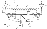
FIG. 1 is a schematic illustration of an exemplary embodiment of an array antenna in accordance with the present invention; -
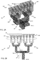
FIGS. 2A and 2B illustrate a perspective view and a front view, respectively, of a first particular example of an array antenna in accordance with the present invention; and -
FIGS. 3A and 3B illustrate a perspective view and a front view, respectively, of a second particular example of an array antenna in accordance with the present invention. - An array antenna as described herein incorporates a phased/coherent cancellation technique to control and to minimize an input reflection coefficient seen at the input of magic T, quadrature coupler or other 4-port device, and the subsequent corporate feed structure thereafter, including subsequent phase correction to support a uniform phase condition at the ports of an ensemble feed. Reflections caused by tolerance variation and/or inadequate bandwidth of components are diverted to a loaded sum or difference port of the magic T, quadrature coupler or other 4-port device, while the difference or the sum port is used for the signal input, respectively. Such configuration improves and broadens the main input reflection coefficient aside from any matching circuitry at the input.
- Referring to
FIG. 1 , anarray antenna 10 is shown schematically. In the exemplary embodiment, thearray antenna 10 is a flat plate array antenna. Thearray antenna 10 is intended for transmitting and/or receiving a plane wave denoted by dashedline 12. Thearray antenna 10 includes a plurality of radiating antenna elements arranged to form an antenna aperture. The plurality of radiating antenna elements are arranged to include a first group of radiatingantenna elements 14A and a second group of radiatingantenna elements 14B, similar in properties but distinct in grouping, from the first group ofradiating antenna elements 14A. In the exemplary embodiment, the first group ofradiating antenna elements 14A and second group of radiatingantenna elements 14B each represent one half of the radiating antenna elements defining the aperture of thearray antenna 10. - The radiating antenna elements may be made up of any suitable known type of array elements such as individual horns in a horn array, slots in a slot array, dipoles in a dipole array, patches in a patch array, etc., as well as any combination thereof. The
array antenna 10 may represent an entire antenna, one of several identical elements making up a larger array, a feed for another antenna system, etc. - The
array antenna 10 further includes acorporate feed network 16 configured to feed the plurality of radiatingantenna elements 14. Thecorporate feed network 16 includes as an input to the array antenna a 4-port device 18 such as a magic T coupler, quadrature hybrid coupler, quadrature hybrid ring coupler or other such suitable 4-port device. The 4-port device 18 includes a sum port (Port 1), a difference port (Port 4), a first signal port (Port 2) and a second signal port (Port 3). The first signal port (Port 2) is coupled via the corporate feed network to the first group of radiating elements and the second signal port (Port 3) is coupled via the corporate feed network to the second group of radiating elements. - A "4-port device" as defined herein refers to any passive 4-port microwave combining device whose microwave (network scattering) properties provide for vector resolution of two independent (signal) ports into two orthogonal vector components via the remaining two (output/input) ports. Orthogonality of the two vector-resolved channels may be in the form of amplitude pairs ("A+B" and "A-B") or alternatively in the form of complex-conjugate pairs ("A+jB" and "B+jA",) depending on the specifics of the particular 4-port device. In the case of the former (amplitude-only) device class, a 90 degree phase-shift (via introduction of a discrete phase-shifter or offset line-length) is added to one of the two signal ports in order to provide the requisite one-way 90 degree phase differential, while this supplemental section is unnecessary when employing a device in the latter (complex-conjugate) class.
- The
corporate feed network 16 may include acorporate feed structure 20 in addition to the 4-port device 18, thecorporate feed structure 20 including any of a variety of conventional corporate feed devices such as couplers, splitters, etc. As described herein, thecorporate feed structure 20 may be divided into afirst portion 20A and asecond portion 20B for feeding the first and second groups of radiatingantenna elements corporate feed structure 20 together with the 4-port device 18 may be constructed using any conventional transmission line approach, including waveguide, microstrip, stripline or other, as will be appreciated. - The
array antenna 10 further includes a firstphase shift element 22 proximal to the antenna aperture to introduce a first predetermined phase shift, via mechanical and/or dielectric means, to the first group of radiatingantenna elements 14A. Additionally, thearray antenna 10 includes a secondphase shift element 24 proximal to the 4-port microwave device 18, at the second signal port (Port 3) to introduce a second predetermined phase shift to the second group of radiatingantenna elements 14B. - The first
phase shift element 22 may include a flat plate dielectric material placed in front of the first group of radiatingantenna elements 14A. For example, the flat plate dielectric material may include air and/or glass as discussed below with respect toFIGS. 2 and3 , respectively. As another example, the firstphase shift element 22 may include a phase-shift line length coupled between the first group of radiatingantenna elements 14A and thecorporate feed network 16. The line length may be made up of waveguide, microstrip, stripline, etc., as will be appreciated. The firstphase shift element 22 preferably is configured to introduce an approximately 90 degree phase shift at mid frequency of an operating band of the array antenna. As referred to herein, "approximately 90 degrees" refers to a phase shift within the range of 90 degrees, plus or minus 20 degrees. - In an embodiment in which the 4-port device includes a magic T coupler, the first signal port (Port 2) and the second signal port (Port 3) represent respective ends of first and second collinear arms included in the magic T coupler. The second
phase shift element 24 is an additional line length in the second collinear arm added to compensate for the phase balance introduced by the firstphase shift element 14A. - In an embodiment where the first
phase shift element 22 is approximately 90 degrees, the secondphase shift element 24 is approximately 90 degrees in length with respect to a mid frequency of an operating band of thearray antenna 10. The secondphase shift element 24 may be made up of waveguide, microstrip, stripline, etc., as will be appreciated. - The 4-
port device 18 may be any of various known types of 4-port devices including, for example, a magic T coupler, a quadrature hybrid coupler, and/or a quadrature hybrid ring coupler. - Continuing to refer to
FIG. 1 , adevice 30 such as a transmitter has its output connected to the sum port (Port 1) of the 4-port device 18. Thedevice 30 outputs a signal (A12+B12) intoPort 1. One half of the signal (A12) is directed towards the first group of radiatingantenna elements 14A viaPort 2 and thefirst portion 20A of thecorporate feed structure 20. The other half of the signal (B12) is directed towards the second group of radiatingantenna elements 14B viaPort 3 and thesecond portion 20B of thecorporate feed structure 20. Undesired reflections at Port 2 (A11) are reflected back intoPort 2 and are directed within the 4-port device 18 to the difference port (Port 4) which is terminated with aload 34 designed to absorb the reflections. Similarly, undesired reflections at Port 3 (B11) are reflected back intoPort 3 and are directed within the 4-port device 18 to the difference port (Port 4) and into theload 34. - It will be appreciated that the
device 30 could be connected to the difference port (Port 4) and theload 34 connected to the sum port (Port 1) and similar operation occurs. - Thus, the
array antenna 10 enjoys a substantial improvement in VSWR by channeling the reflection caused by tolerance variation and/or inadequate components' bandwidth to the "loaded" sum or difference ports of the magic T, quadrature coupler or other 4-port device, while the difference or the sum port used for the signal input, respectively. Degradation in the input reflection or the radiation pattern is avoided since the phase change in half of the aperture is corrected by the introduction of the secondphase shift element 24 while the undesired reflection is channeled into the loaded arm of the 4-way power divider isolated from main input. Thearray antenna 10 thus presents the simplicity of using a piece of flat plate dielectric plus simple phase adjustment (e.g., in the collinear arms of a magic T) to achieve broader bandwidth without complicated matching circuitry at the input. - In exemplary embodiments, a half aperture sized flat plate dielectric material serving as the first
phase shift element 22 is placed in front of the first group of radiatingantenna elements 14A representing one half of the antenna aperture. At the same time, the 4-port device 18 feeding the entire aperture includes a purposeful phase shift in the form of the secondphase shift element 24 to compensate for the phase imbalance in the aperture introduced by the firstphase shift element 22. This intentional phase shift at the aperture and the 4-port device provides desired VSWR cancellation properties. - The half aperture sized flat plate dielectric material serving as the first
phase shift element 22 should be a half wavelength (wavelength inside the dielectric medium) thick around the mid frequency of the operating band of thearray antenna 10. Ideally, glass material with the dielectric constant of 4 can provide the thickness which is exactly the quarter of wavelength in free space and translates to a 90 degrees phase shift in free space. However, in the absence of the glass other dielectric materials, with appropriate thicknesses, can also be used to achieve similar improvement, while departing from a rigorous half-wavelength thickness criteria. Alternatively, multi-layer embodiments may be employed as the phase-shift element 22, in order to simultaneously provide both the desired insertion phase correction and desired input match properties. - Referring to
Figs. 2A-2B , shown is a first particular embodiment of the present invention as described herein. The first group of radiatingantenna elements 14A is made up of four radiatingantenna elements 14 coupled toPort 2 of the 4-port device 18 via a 1-to-4 power dividercorporate feed structure 20A. Similarly, the second group of radiatingantenna elements 14B is made up of four radiatingantenna elements 14 coupled toPort 3 of the 4-port device 18 via a 1-to-4 power dividercorporate feed structure 20B. - The 4-
port device 18 in this embodiment is a 4-port waveguide magic-T. Moreover, in this embodiment the firstphase shift element 22 is made up of a recessed half aperture. In this manner, the first phase shift element is anair dielectric 22a and is configured to introduce an approximately 90 degree phase shift at mid frequency of an operating band of the array antenna. To offset the radiated phase impact due to the introduction of theair dielectric 22a, the 4-port device 18 includes phase imbalanced collinear arms. Specifically, the collinear arm atPort 3 includes an additional 90 degree feed-line length representing the secondphase shift element 24. -
Figs. 3A and 3B illustrate another particular embodiment similar to the embodiment ofFigs. 2A-2B but with the following exceptions. Rather than theair dielectric 22a,dielectric plate 22b is introduced at the antenna aperture in front of the radiatingantenna elements 14A. To offset the radiated phase impact due to the introduction of thedielectric plate 22b, the 4-port device 18 again includes phase imbalanced collinear arms. Specifically, the collinear arm atPort 3 includes an additional 90 degree feed-line length representing the secondphase shift element 24. - Although the invention has been shown and described with respect to a certain embodiment or embodiments, equivalent alterations and modifications may occur to others skilled in the art upon the reading and understanding of this specification and the annexed drawings. In particular regard to the various functions performed by the above described elements (components, assemblies, devices, compositions, etc.), the terms (including a reference to a "means") used to describe such elements are intended to correspond, unless otherwise indicated, to any element which performs the specified function of the described element (i.e., that is functionally equivalent), even though not structurally equivalent to the disclosed structure which performs the function in the herein exemplary embodiment or embodiments of the invention. In addition, while a particular feature of the invention may have been described above with respect to only one or more of several embodiments, such feature may be combined with one or more other features of the other embodiments, as may be desired and advantageous for any given or particular application.
Claims (10)
- An array antenna (10), comprising:a plurality of radiating antenna elements arranged to form an antenna aperture, the plurality of radiating antenna elements including a first group of radiating antenna elements (14a) and a second group of radiating antenna elements (14b) distinct in grouping from the first group of radiating antenna elements;a corporate feed network (16) configured to feed the plurality of radiating antenna elements, wherein the corporate feed network includes a 4-port device (18) comprising a sum port (Port 1), a difference port (Port 4), a first signal port (Port 2) and a second signal port (Port 3), with the first signal port coupled via the corporate feed network to the first group of radiating elements and the second signal port coupled via the corporate feed network to the second group of radiating elements;a first phase shift element (22) connected between the first group of radiating antenna elements and the first signal port, wherein said first phase shift element is configured to introduce a predetermined phase shift to the first group of radiating antenna elements; anda second phase shift element (24) located within the 4-port device (18) and being configured such that the second signal port introduces a second predetermined phase shift to the second group of radiating antenna elements.
- The array antenna according to claim 1, wherein the first group of radiating antenna elements (14a) and the second group of radiating antenna elements (14b) each represent a corresponding half of the antenna aperture
- The array antenna according to any one of claims 1-2, wherein the first phase shift element (22) comprises a flat plate dielectric material (22b) placed in front of the first group of radiating antenna elements.
- The array antenna according to claim 3, wherein the flat plate dielectric material (22b) includes glass and/or air.
- The array antenna according to any one of claims 1-2, wherein the first phase shift element (22) comprises a phase-shift line length coupled between the first group of radiating antenna elements and the corporate feed network.
- The array antenna according to any one of claims 1-5, wherein the first phase shift element (22) introduces an approximately 90 degree phase shift at mid-frequency of an operating band of the array antenna.
- The array antenna according to any one of claims 1-6, wherein the first signal port (Port 2) and the second signal port (Port 3) represent respective ends of first and second collinear arms included in the 4-port device, and the second phase shift element comprises an additional line length in the second collinear arm.
- The array antenna according to claim 7, wherein the second phase shift element (24) is approximately 90 degrees in length with respect to a mid-frequency of an operating band of the array antenna.
- The array antenna according to any one of claims 1-8, wherein the 4-port device is a magic T-coupler, a quadrature hybrid coupler, and/or a quadrature hybrid ring coupler.
- The array antenna according to any one of claims 1 -9, wherein the corporate feed network is made up of waveguide, microstrip and/or stripline components.
Applications Claiming Priority (1)
| Application Number | Priority Date | Filing Date | Title |
|---|---|---|---|
| US14/246,264 US9257753B2 (en) | 2014-04-07 | 2014-04-07 | Array antenna |
Publications (2)
| Publication Number | Publication Date |
|---|---|
| EP2930790A1 EP2930790A1 (en) | 2015-10-14 |
| EP2930790B1 true EP2930790B1 (en) | 2017-03-22 |
Family
ID=52807706
Family Applications (1)
| Application Number | Title | Priority Date | Filing Date |
|---|---|---|---|
| EP15162366.7A Active EP2930790B1 (en) | 2014-04-07 | 2015-04-02 | Array antenna |
Country Status (5)
| Country | Link |
|---|---|
| US (1) | US9257753B2 (en) |
| EP (1) | EP2930790B1 (en) |
| CA (1) | CA2887073C (en) |
| ES (1) | ES2623767T3 (en) |
| IL (1) | IL237994B (en) |
Families Citing this family (12)
| Publication number | Priority date | Publication date | Assignee | Title |
|---|---|---|---|---|
| US9543644B2 (en) * | 2014-07-01 | 2017-01-10 | The Chinese University Of Hong Kong | Method and an apparatus for decoupling multiple antennas in a compact antenna array |
| CN106450763B (en) * | 2016-11-25 | 2024-02-23 | 京信通信技术(广州)有限公司 | Dielectric phase shift unit, dielectric phase shifter and base station antenna |
| FR3061364B1 (en) * | 2016-12-22 | 2020-06-19 | Thales | MECHANICAL ARCHITECTURE OF A BEAM FORMER FOR SINGLE-SOURCE SINGLE-SOURCE MFPB ANTENNA MFPB ACCORDING TO TWO SPACE DIMENSIONS AND METHOD FOR PRODUCING THE BEAM FORMER |
| CN107634301B (en) * | 2017-09-02 | 2020-04-17 | 南京理工大学 | Magic plane T with common mode rejection function |
| US10840605B2 (en) * | 2017-12-20 | 2020-11-17 | Optisys, LLC | Integrated linearly polarized tracking antenna array |
| US11101573B2 (en) * | 2018-07-02 | 2021-08-24 | Sea Tel, Inc. | Open ended waveguide antenna for one-dimensional active arrays |
| EP3861596A1 (en) * | 2018-10-02 | 2021-08-11 | Teknologian tutkimuskeskus VTT Oy | Phased array antenna system with a fixed feed antenna |
| US12183963B2 (en) | 2020-10-19 | 2024-12-31 | Optisys, Inc. | Device comprising a transition between a waveguide port and two or more coaxial waveguides |
| EP4238185A4 (en) | 2020-10-29 | 2024-10-02 | Optisys, Inc. | INTEGRATED BALANCED RADIATION ELEMENTS |
| US12009596B2 (en) | 2021-05-14 | 2024-06-11 | Optisys, Inc. | Planar monolithic combiner and multiplexer for antenna arrays |
| WO2023070350A1 (en) * | 2021-10-27 | 2023-05-04 | 京东方科技集团股份有限公司 | Antenna |
| CN117157833A (en) * | 2022-02-28 | 2023-12-01 | 京东方科技集团股份有限公司 | Phased array antenna |
Family Cites Families (7)
| Publication number | Priority date | Publication date | Assignee | Title |
|---|---|---|---|---|
| US6064350A (en) * | 1997-07-25 | 2000-05-16 | Kyocera Corporation | Laminated aperture-faced antenna and multi-layered wiring board comprising the same |
| US6201508B1 (en) * | 1999-12-13 | 2001-03-13 | Space Systems/Loral, Inc. | Injection-molded phased array antenna system |
| US8081115B2 (en) * | 2007-11-15 | 2011-12-20 | Raytheon Company | Combining multiple-port patch antenna |
| ES2399315T3 (en) * | 2008-04-29 | 2013-03-27 | Raytheon Company | Small aperture interrogator antenna system that uses sum-difference azimuth discrimination techniques |
| US7737904B2 (en) * | 2008-06-11 | 2010-06-15 | Lockheed Martin Corporation | Antenna systems for multiple frequency bands |
| EP2685557B1 (en) * | 2012-04-20 | 2019-09-11 | Huawei Technologies Co., Ltd. | Antenna and base station |
| US9413079B2 (en) * | 2013-03-13 | 2016-08-09 | Intel Corporation | Single-package phased array module with interleaved sub-arrays |
-
2014
- 2014-04-07 US US14/246,264 patent/US9257753B2/en active Active
-
2015
- 2015-03-29 IL IL237994A patent/IL237994B/en active IP Right Grant
- 2015-04-02 ES ES15162366.7T patent/ES2623767T3/en active Active
- 2015-04-02 EP EP15162366.7A patent/EP2930790B1/en active Active
- 2015-04-02 CA CA2887073A patent/CA2887073C/en active Active
Non-Patent Citations (1)
| Title |
|---|
| None * |
Also Published As
| Publication number | Publication date |
|---|---|
| EP2930790A1 (en) | 2015-10-14 |
| IL237994B (en) | 2018-07-31 |
| ES2623767T3 (en) | 2017-07-12 |
| IL237994A0 (en) | 2015-11-30 |
| CA2887073C (en) | 2021-10-26 |
| CA2887073A1 (en) | 2015-10-07 |
| US20150288075A1 (en) | 2015-10-08 |
| US9257753B2 (en) | 2016-02-09 |
Similar Documents
| Publication | Publication Date | Title |
|---|---|---|
| US9257753B2 (en) | Array antenna | |
| KR102302466B1 (en) | Waveguide slotted array antenna | |
| US12424747B2 (en) | Multiband resonator element for making filters, polarizers and frequency-selective surfaces | |
| US20130057447A1 (en) | Calibration of active antenna arrays for mobile telecommunications | |
| CN104332713B (en) | Monolayer double frequency round polarized micro-strip array antenna | |
| CN106898882A (en) | Suitable for the multi-beam back cavity type high-gain aerial battle array of millimetre-wave attenuator | |
| WO2016179799A1 (en) | Double-frequency phased array | |
| Nguyen et al. | Pencil-beam full-space scanning 2D CRLH leaky-wave antenna array | |
| Lee et al. | A circularly polarized single radiator leaky-wave antenna based on CRLH-inspired substrate integrated waveguide | |
| CN204407491U (en) | Antenna, antenna system and communication equipment | |
| CN204407484U (en) | Antenna, antenna system and communication equipment | |
| CN204407500U (en) | Antenna, antenna system and communication equipment | |
| Ji et al. | Array-fed beam-scanning partially reflective surface (PRS) antenna | |
| Islam et al. | E‐Band Beam‐Steerable and Scalable Phased Antenna Array for 5G Access Point | |
| CN204407494U (en) | Antenna, antenna system and communication equipment | |
| Kim et al. | A heterodyne-scan phased-array antenna | |
| Orakwue et al. | Switched-beam array antenna at 28 GHz for 5G wireless system based on butler matrix beamforming network | |
| Lele et al. | Reflectarray antennas | |
| Nassar et al. | Beam steering antenna arrays for 28-GHz applications | |
| Jayachitra et al. | Design of hybrid coupler | |
| JP2018093387A (en) | Antenna feed circuit | |
| CN204407498U (en) | Antenna, antenna system and communication equipment | |
| Kim et al. | School of Electronic and Electrical Engineering Hongik University, Seoul, Korea | |
| Guo et al. | A 2× 3 Hybrid Substrate Integrated Waveguide Coupler Applied to Beamforming Network | |
| Kim et al. | A tapered slot antenna for beamforming application |
Legal Events
| Date | Code | Title | Description |
|---|---|---|---|
| PUAI | Public reference made under article 153(3) epc to a published international application that has entered the european phase |
Free format text: ORIGINAL CODE: 0009012 |
|
| AK | Designated contracting states |
Kind code of ref document: A1 Designated state(s): AL AT BE BG CH CY CZ DE DK EE ES FI FR GB GR HR HU IE IS IT LI LT LU LV MC MK MT NL NO PL PT RO RS SE SI SK SM TR |
|
| AX | Request for extension of the european patent |
Extension state: BA ME |
|
| 17P | Request for examination filed |
Effective date: 20160408 |
|
| RBV | Designated contracting states (corrected) |
Designated state(s): AL AT BE BG CH CY CZ DE DK EE ES FI FR GB GR HR HU IE IS IT LI LT LU LV MC MK MT NL NO PL PT RO RS SE SI SK SM TR |
|
| REG | Reference to a national code |
Ref country code: DE Ref legal event code: R079 Ref document number: 602015001876 Country of ref document: DE Free format text: PREVIOUS MAIN CLASS: H01Q0025020000 Ipc: H01Q0021000000 |
|
| GRAP | Despatch of communication of intention to grant a patent |
Free format text: ORIGINAL CODE: EPIDOSNIGR1 |
|
| RIC1 | Information provided on ipc code assigned before grant |
Ipc: H01Q 21/00 20060101AFI20160915BHEP Ipc: H01Q 25/02 20060101ALI20160915BHEP Ipc: H01Q 15/08 20060101ALI20160915BHEP Ipc: H01Q 3/30 20060101ALI20160915BHEP Ipc: H01Q 3/26 20060101ALI20160915BHEP |
|
| INTG | Intention to grant announced |
Effective date: 20160929 |
|
| GRAS | Grant fee paid |
Free format text: ORIGINAL CODE: EPIDOSNIGR3 |
|
| STAA | Information on the status of an ep patent application or granted ep patent |
Free format text: STATUS: GRANT OF PATENT IS INTENDED |
|
| GRAA | (expected) grant |
Free format text: ORIGINAL CODE: 0009210 |
|
| STAA | Information on the status of an ep patent application or granted ep patent |
Free format text: STATUS: THE PATENT HAS BEEN GRANTED |
|
| AK | Designated contracting states |
Kind code of ref document: B1 Designated state(s): AL AT BE BG CH CY CZ DE DK EE ES FI FR GB GR HR HU IE IS IT LI LT LU LV MC MK MT NL NO PL PT RO RS SE SI SK SM TR |
|
| REG | Reference to a national code |
Ref country code: GB Ref legal event code: FG4D |
|
| REG | Reference to a national code |
Ref country code: CH Ref legal event code: EP |
|
| REG | Reference to a national code |
Ref country code: AT Ref legal event code: REF Ref document number: 878592 Country of ref document: AT Kind code of ref document: T Effective date: 20170415 |
|
| REG | Reference to a national code |
Ref country code: FR Ref legal event code: PLFP Year of fee payment: 3 Ref country code: IE Ref legal event code: FG4D |
|
| REG | Reference to a national code |
Ref country code: DE Ref legal event code: R096 Ref document number: 602015001876 Country of ref document: DE |
|
| REG | Reference to a national code |
Ref country code: ES Ref legal event code: FG2A Ref document number: 2623767 Country of ref document: ES Kind code of ref document: T3 Effective date: 20170712 |
|
| REG | Reference to a national code |
Ref country code: NL Ref legal event code: MP Effective date: 20170322 |
|
| PG25 | Lapsed in a contracting state [announced via postgrant information from national office to epo] |
Ref country code: HR Free format text: LAPSE BECAUSE OF FAILURE TO SUBMIT A TRANSLATION OF THE DESCRIPTION OR TO PAY THE FEE WITHIN THE PRESCRIBED TIME-LIMIT Effective date: 20170322 Ref country code: NO Free format text: LAPSE BECAUSE OF FAILURE TO SUBMIT A TRANSLATION OF THE DESCRIPTION OR TO PAY THE FEE WITHIN THE PRESCRIBED TIME-LIMIT Effective date: 20170622 Ref country code: GR Free format text: LAPSE BECAUSE OF FAILURE TO SUBMIT A TRANSLATION OF THE DESCRIPTION OR TO PAY THE FEE WITHIN THE PRESCRIBED TIME-LIMIT Effective date: 20170623 Ref country code: LT Free format text: LAPSE BECAUSE OF FAILURE TO SUBMIT A TRANSLATION OF THE DESCRIPTION OR TO PAY THE FEE WITHIN THE PRESCRIBED TIME-LIMIT Effective date: 20170322 Ref country code: FI Free format text: LAPSE BECAUSE OF FAILURE TO SUBMIT A TRANSLATION OF THE DESCRIPTION OR TO PAY THE FEE WITHIN THE PRESCRIBED TIME-LIMIT Effective date: 20170322 |
|
| REG | Reference to a national code |
Ref country code: LT Ref legal event code: MG4D |
|
| REG | Reference to a national code |
Ref country code: AT Ref legal event code: MK05 Ref document number: 878592 Country of ref document: AT Kind code of ref document: T Effective date: 20170322 |
|
| PG25 | Lapsed in a contracting state [announced via postgrant information from national office to epo] |
Ref country code: LV Free format text: LAPSE BECAUSE OF FAILURE TO SUBMIT A TRANSLATION OF THE DESCRIPTION OR TO PAY THE FEE WITHIN THE PRESCRIBED TIME-LIMIT Effective date: 20170322 Ref country code: SE Free format text: LAPSE BECAUSE OF FAILURE TO SUBMIT A TRANSLATION OF THE DESCRIPTION OR TO PAY THE FEE WITHIN THE PRESCRIBED TIME-LIMIT Effective date: 20170322 Ref country code: RS Free format text: LAPSE BECAUSE OF FAILURE TO SUBMIT A TRANSLATION OF THE DESCRIPTION OR TO PAY THE FEE WITHIN THE PRESCRIBED TIME-LIMIT Effective date: 20170322 Ref country code: BG Free format text: LAPSE BECAUSE OF FAILURE TO SUBMIT A TRANSLATION OF THE DESCRIPTION OR TO PAY THE FEE WITHIN THE PRESCRIBED TIME-LIMIT Effective date: 20170622 |
|
| PG25 | Lapsed in a contracting state [announced via postgrant information from national office to epo] |
Ref country code: NL Free format text: LAPSE BECAUSE OF FAILURE TO SUBMIT A TRANSLATION OF THE DESCRIPTION OR TO PAY THE FEE WITHIN THE PRESCRIBED TIME-LIMIT Effective date: 20170322 |
|
| PG25 | Lapsed in a contracting state [announced via postgrant information from national office to epo] |
Ref country code: EE Free format text: LAPSE BECAUSE OF FAILURE TO SUBMIT A TRANSLATION OF THE DESCRIPTION OR TO PAY THE FEE WITHIN THE PRESCRIBED TIME-LIMIT Effective date: 20170322 Ref country code: CZ Free format text: LAPSE BECAUSE OF FAILURE TO SUBMIT A TRANSLATION OF THE DESCRIPTION OR TO PAY THE FEE WITHIN THE PRESCRIBED TIME-LIMIT Effective date: 20170322 Ref country code: SK Free format text: LAPSE BECAUSE OF FAILURE TO SUBMIT A TRANSLATION OF THE DESCRIPTION OR TO PAY THE FEE WITHIN THE PRESCRIBED TIME-LIMIT Effective date: 20170322 Ref country code: RO Free format text: LAPSE BECAUSE OF FAILURE TO SUBMIT A TRANSLATION OF THE DESCRIPTION OR TO PAY THE FEE WITHIN THE PRESCRIBED TIME-LIMIT Effective date: 20170322 Ref country code: AT Free format text: LAPSE BECAUSE OF FAILURE TO SUBMIT A TRANSLATION OF THE DESCRIPTION OR TO PAY THE FEE WITHIN THE PRESCRIBED TIME-LIMIT Effective date: 20170322 |
|
| PG25 | Lapsed in a contracting state [announced via postgrant information from national office to epo] |
Ref country code: IS Free format text: LAPSE BECAUSE OF FAILURE TO SUBMIT A TRANSLATION OF THE DESCRIPTION OR TO PAY THE FEE WITHIN THE PRESCRIBED TIME-LIMIT Effective date: 20170722 Ref country code: PT Free format text: LAPSE BECAUSE OF FAILURE TO SUBMIT A TRANSLATION OF THE DESCRIPTION OR TO PAY THE FEE WITHIN THE PRESCRIBED TIME-LIMIT Effective date: 20170724 Ref country code: SM Free format text: LAPSE BECAUSE OF FAILURE TO SUBMIT A TRANSLATION OF THE DESCRIPTION OR TO PAY THE FEE WITHIN THE PRESCRIBED TIME-LIMIT Effective date: 20170322 Ref country code: PL Free format text: LAPSE BECAUSE OF FAILURE TO SUBMIT A TRANSLATION OF THE DESCRIPTION OR TO PAY THE FEE WITHIN THE PRESCRIBED TIME-LIMIT Effective date: 20170322 |
|
| REG | Reference to a national code |
Ref country code: DE Ref legal event code: R097 Ref document number: 602015001876 Country of ref document: DE |
|
| REG | Reference to a national code |
Ref country code: IE Ref legal event code: MM4A |
|
| PLBE | No opposition filed within time limit |
Free format text: ORIGINAL CODE: 0009261 |
|
| STAA | Information on the status of an ep patent application or granted ep patent |
Free format text: STATUS: NO OPPOSITION FILED WITHIN TIME LIMIT |
|
| PG25 | Lapsed in a contracting state [announced via postgrant information from national office to epo] |
Ref country code: MC Free format text: LAPSE BECAUSE OF FAILURE TO SUBMIT A TRANSLATION OF THE DESCRIPTION OR TO PAY THE FEE WITHIN THE PRESCRIBED TIME-LIMIT Effective date: 20170322 Ref country code: DK Free format text: LAPSE BECAUSE OF FAILURE TO SUBMIT A TRANSLATION OF THE DESCRIPTION OR TO PAY THE FEE WITHIN THE PRESCRIBED TIME-LIMIT Effective date: 20170322 |
|
| 26N | No opposition filed |
Effective date: 20180102 |
|
| PG25 | Lapsed in a contracting state [announced via postgrant information from national office to epo] |
Ref country code: LU Free format text: LAPSE BECAUSE OF NON-PAYMENT OF DUE FEES Effective date: 20170402 Ref country code: SI Free format text: LAPSE BECAUSE OF FAILURE TO SUBMIT A TRANSLATION OF THE DESCRIPTION OR TO PAY THE FEE WITHIN THE PRESCRIBED TIME-LIMIT Effective date: 20170322 |
|
| REG | Reference to a national code |
Ref country code: BE Ref legal event code: MM Effective date: 20170430 |
|
| REG | Reference to a national code |
Ref country code: FR Ref legal event code: PLFP Year of fee payment: 4 |
|
| PG25 | Lapsed in a contracting state [announced via postgrant information from national office to epo] |
Ref country code: IE Free format text: LAPSE BECAUSE OF NON-PAYMENT OF DUE FEES Effective date: 20170402 |
|
| PG25 | Lapsed in a contracting state [announced via postgrant information from national office to epo] |
Ref country code: BE Free format text: LAPSE BECAUSE OF NON-PAYMENT OF DUE FEES Effective date: 20170430 |
|
| PG25 | Lapsed in a contracting state [announced via postgrant information from national office to epo] |
Ref country code: MT Free format text: LAPSE BECAUSE OF NON-PAYMENT OF DUE FEES Effective date: 20170402 |
|
| REG | Reference to a national code |
Ref country code: CH Ref legal event code: PL |
|
| PG25 | Lapsed in a contracting state [announced via postgrant information from national office to epo] |
Ref country code: CH Free format text: LAPSE BECAUSE OF NON-PAYMENT OF DUE FEES Effective date: 20180430 Ref country code: LI Free format text: LAPSE BECAUSE OF NON-PAYMENT OF DUE FEES Effective date: 20180430 |
|
| PG25 | Lapsed in a contracting state [announced via postgrant information from national office to epo] |
Ref country code: HU Free format text: LAPSE BECAUSE OF FAILURE TO SUBMIT A TRANSLATION OF THE DESCRIPTION OR TO PAY THE FEE WITHIN THE PRESCRIBED TIME-LIMIT; INVALID AB INITIO Effective date: 20150402 |
|
| PG25 | Lapsed in a contracting state [announced via postgrant information from national office to epo] |
Ref country code: CY Free format text: LAPSE BECAUSE OF FAILURE TO SUBMIT A TRANSLATION OF THE DESCRIPTION OR TO PAY THE FEE WITHIN THE PRESCRIBED TIME-LIMIT Effective date: 20170322 |
|
| PG25 | Lapsed in a contracting state [announced via postgrant information from national office to epo] |
Ref country code: MK Free format text: LAPSE BECAUSE OF FAILURE TO SUBMIT A TRANSLATION OF THE DESCRIPTION OR TO PAY THE FEE WITHIN THE PRESCRIBED TIME-LIMIT Effective date: 20170322 |
|
| PG25 | Lapsed in a contracting state [announced via postgrant information from national office to epo] |
Ref country code: TR Free format text: LAPSE BECAUSE OF FAILURE TO SUBMIT A TRANSLATION OF THE DESCRIPTION OR TO PAY THE FEE WITHIN THE PRESCRIBED TIME-LIMIT Effective date: 20170322 |
|
| PG25 | Lapsed in a contracting state [announced via postgrant information from national office to epo] |
Ref country code: AL Free format text: LAPSE BECAUSE OF FAILURE TO SUBMIT A TRANSLATION OF THE DESCRIPTION OR TO PAY THE FEE WITHIN THE PRESCRIBED TIME-LIMIT Effective date: 20170322 |
|
| REG | Reference to a national code |
Ref country code: ES Ref legal event code: FD2A Effective date: 20200828 |
|
| PG25 | Lapsed in a contracting state [announced via postgrant information from national office to epo] |
Ref country code: ES Free format text: LAPSE BECAUSE OF NON-PAYMENT OF DUE FEES Effective date: 20190403 |
|
| REG | Reference to a national code |
Ref country code: ES Ref legal event code: NE2A Effective date: 20210415 |
|
| PG25 | Lapsed in a contracting state [announced via postgrant information from national office to epo] |
Ref country code: ES Free format text: LAPSE BECAUSE OF NON-PAYMENT OF DUE FEES Effective date: 20190403 |
|
| PGRI | Patent reinstated in contracting state [announced from national office to epo] |
Ref country code: ES Effective date: 20210415 |
|
| P01 | Opt-out of the competence of the unified patent court (upc) registered |
Effective date: 20230525 |
|
| PGFP | Annual fee paid to national office [announced via postgrant information from national office to epo] |
Ref country code: DE Payment date: 20250515 Year of fee payment: 11 |
|
| PGFP | Annual fee paid to national office [announced via postgrant information from national office to epo] |
Ref country code: GB Payment date: 20250520 Year of fee payment: 11 Ref country code: ES Payment date: 20250523 Year of fee payment: 11 |
|
| PGFP | Annual fee paid to national office [announced via postgrant information from national office to epo] |
Ref country code: IT Payment date: 20250520 Year of fee payment: 11 |
|
| PGFP | Annual fee paid to national office [announced via postgrant information from national office to epo] |
Ref country code: FR Payment date: 20250515 Year of fee payment: 11 |