EP2930739A1 - Super-junction manufacturing method - Google Patents
Super-junction manufacturing method Download PDFInfo
- Publication number
- EP2930739A1 EP2930739A1 EP12889660.2A EP12889660A EP2930739A1 EP 2930739 A1 EP2930739 A1 EP 2930739A1 EP 12889660 A EP12889660 A EP 12889660A EP 2930739 A1 EP2930739 A1 EP 2930739A1
- Authority
- EP
- European Patent Office
- Prior art keywords
- heavily doped
- type heavily
- doped substrate
- doped region
- super
- Prior art date
- Legal status (The legal status is an assumption and is not a legal conclusion. Google has not performed a legal analysis and makes no representation as to the accuracy of the status listed.)
- Granted
Links
Images

Classifications
-
- H—ELECTRICITY
- H10—SEMICONDUCTOR DEVICES; ELECTRIC SOLID-STATE DEVICES NOT OTHERWISE PROVIDED FOR
- H10P—GENERIC PROCESSES OR APPARATUS FOR THE MANUFACTURE OR TREATMENT OF DEVICES COVERED BY CLASS H10
- H10P34/00—Irradiation with electromagnetic or particle radiation of wafers, substrates or parts of devices
- H10P34/40—Irradiation with electromagnetic or particle radiation of wafers, substrates or parts of devices with high-energy radiation
-
- H—ELECTRICITY
- H10—SEMICONDUCTOR DEVICES; ELECTRIC SOLID-STATE DEVICES NOT OTHERWISE PROVIDED FOR
- H10D—INORGANIC ELECTRIC SEMICONDUCTOR DEVICES
- H10D62/00—Semiconductor bodies, or regions thereof, of devices having potential barriers
- H10D62/01—Manufacture or treatment
- H10D62/051—Forming charge compensation regions, e.g. superjunctions
- H10D62/054—Forming charge compensation regions, e.g. superjunctions by high energy implantations in bulk semiconductor bodies, e.g. forming pillars
-
- H—ELECTRICITY
- H10—SEMICONDUCTOR DEVICES; ELECTRIC SOLID-STATE DEVICES NOT OTHERWISE PROVIDED FOR
- H10D—INORGANIC ELECTRIC SEMICONDUCTOR DEVICES
- H10D62/00—Semiconductor bodies, or regions thereof, of devices having potential barriers
- H10D62/10—Shapes, relative sizes or dispositions of the regions of the semiconductor bodies; Shapes of the semiconductor bodies
- H10D62/102—Constructional design considerations for preventing surface leakage or controlling electric field concentration
- H10D62/103—Constructional design considerations for preventing surface leakage or controlling electric field concentration for increasing or controlling the breakdown voltage of reverse-biased devices
- H10D62/105—Constructional design considerations for preventing surface leakage or controlling electric field concentration for increasing or controlling the breakdown voltage of reverse-biased devices by having particular doping profiles, shapes or arrangements of PN junctions; by having supplementary regions, e.g. junction termination extension [JTE]
- H10D62/109—Reduced surface field [RESURF] PN junction structures
- H10D62/111—Multiple RESURF structures, e.g. double RESURF or 3D-RESURF structures
-
- H—ELECTRICITY
- H10—SEMICONDUCTOR DEVICES; ELECTRIC SOLID-STATE DEVICES NOT OTHERWISE PROVIDED FOR
- H10P—GENERIC PROCESSES OR APPARATUS FOR THE MANUFACTURE OR TREATMENT OF DEVICES COVERED BY CLASS H10
- H10P34/00—Irradiation with electromagnetic or particle radiation of wafers, substrates or parts of devices
- H10P34/20—Irradiation with electromagnetic or particle radiation of wafers, substrates or parts of devices for inducing a nuclear reaction transmuting chemical elements
-
- H—ELECTRICITY
- H10—SEMICONDUCTOR DEVICES; ELECTRIC SOLID-STATE DEVICES NOT OTHERWISE PROVIDED FOR
- H10D—INORGANIC ELECTRIC SEMICONDUCTOR DEVICES
- H10D12/00—Bipolar devices controlled by the field effect, e.g. insulated-gate bipolar transistors [IGBT]
- H10D12/01—Manufacture or treatment
- H10D12/031—Manufacture or treatment of IGBTs
- H10D12/032—Manufacture or treatment of IGBTs of vertical IGBTs
-
- H—ELECTRICITY
- H10—SEMICONDUCTOR DEVICES; ELECTRIC SOLID-STATE DEVICES NOT OTHERWISE PROVIDED FOR
- H10D—INORGANIC ELECTRIC SEMICONDUCTOR DEVICES
- H10D12/00—Bipolar devices controlled by the field effect, e.g. insulated-gate bipolar transistors [IGBT]
- H10D12/411—Insulated-gate bipolar transistors [IGBT]
- H10D12/441—Vertical IGBTs
-
- H—ELECTRICITY
- H10—SEMICONDUCTOR DEVICES; ELECTRIC SOLID-STATE DEVICES NOT OTHERWISE PROVIDED FOR
- H10D—INORGANIC ELECTRIC SEMICONDUCTOR DEVICES
- H10D30/00—Field-effect transistors [FET]
- H10D30/01—Manufacture or treatment
- H10D30/021—Manufacture or treatment of FETs having insulated gates [IGFET]
- H10D30/028—Manufacture or treatment of FETs having insulated gates [IGFET] of double-diffused metal oxide semiconductor [DMOS] FETs
- H10D30/0291—Manufacture or treatment of FETs having insulated gates [IGFET] of double-diffused metal oxide semiconductor [DMOS] FETs of vertical DMOS [VDMOS] FETs
-
- H—ELECTRICITY
- H10—SEMICONDUCTOR DEVICES; ELECTRIC SOLID-STATE DEVICES NOT OTHERWISE PROVIDED FOR
- H10D—INORGANIC ELECTRIC SEMICONDUCTOR DEVICES
- H10D8/00—Diodes
- H10D8/50—PIN diodes
Definitions
- the present disclosure relates to the field of semiconductor manufacturing technology, and particularly to a method for manufacturing a super-junction.
- a traditional process for manufacturing a super-junction is an ion implantation process or a grooving and filling process.
- the ion implantation process mainly adopts a high energy ion implantation process or a repeated epitaxy and implantation process.
- the grooving and filling process mainly adopts a deep reactive ion etching process, or a repeated epitaxy, grooving and filling process.
- a method for manufacturing a super-junction is provided according to embodiments of the present disclosure, in order to simplify a manufacturing process of a super-junction and reduce the manufacture cost.
- a method for manufacturing a super-junction which includes:
- the lightly doped substrate may be made of silicon, silicon carbide, gallium arsenide, or indium antimonide.
- the forming a p-type heavily doped region within the lightly doped substrate through a transmutation doping process may include: forming a high-energy photon beam by using a photon source; and forming a p-type heavily doped region within the lightly doped substrate by a nuclear reaction started by particle radiation on the lightly doped substrate by using the high-energy photon beam.
- the photon source may be an electronic linear accelerator photon source.
- the energy of the high-energy photon beam may range from 17.5 MeV to 22.5 MeV.
- the first mask may be made of high-energy photon absorber.
- the forming an n-type heavily doped region within the lightly doped substrate through a transmutation doping process may include: forming a neutron beam by using a neutron source; and forming an n-type heavily doped region within the lightly doped substrate by a nuclear reaction started by particle radiation on the lightly doped substrate by using the neutron beam.
- the neutron source may be a radioisotope neutron source, an accelerator neutron source, or a reactor neutron source.
- the second mask may be made of neutron absorber.
- a method for manufacturing a super-junction which includes:
- the first-type heavily doped substrate may be a p-type heavily doped substrate, and the second second-type heavily doped region may be an n-type heavily doped region.
- the first-type heavily doped substrate may be made of silicon, silicon carbide, gallium arsenide, or indium antimonide.
- the forming a second-type heavily doped region within the first-type heavily doped substrate through a transmutation doping process may include: forming a neutron beam by using a neutron source; and forming a second-type heavily doped region within the first-type heavily doped substrate by a nuclear reaction started by particle radiation on the first-type heavily doped substrate by using the neutron beam to ignite.
- the first-type heavily doped substrate may be an n-type heavily doped substrate, and the second-type heavily doped region may be a p-type heavily doped region.
- the first-type heavily doped substrate may be made of silicon, silicon carbide, diamond, germanium, gallium arsenide, or indium antimonide.
- the forming a second-type heavily doped region within the first-type heavily doped substrate through a transmutation doping process may include: forming a high-energy photon beam by using a photon source; and forming a second-type heavily doped region within the first-type heavily doped substrate by a nuclear reaction started by particle radiation on the first-type heavily doped substrate by using the high-energy photon beam.
- the first-type heavily doped substrate may be made of germanium.
- the forming a second-type heavily doped region within the first-type heavily doped substrate through a transmutation doping process may include: forming a neutron beam by using a neutron source; and forming a second-type heavily doped region within the first-type heavily doped substrate by a nuclear reaction started by particle radiation on the first-type heavily doped substrate by using the neutron beam.
- a super-junction manufactured by any one of the methods described above is provided.
- a super-junction semiconductor device is provided, where a super-junction in the super-junction semiconductor device is the super-junction described above.
- a p-type heavily doped region and an n-type heavily doped region are formed within a lightly doped substrate through a transmutation doping process.
- a second-type heavily doped region is formed within the first-type heavily doped substrate through a transmutation doping process.
- a doped region within a substrate is obtained by a nuclear reaction, i.e., a super-junction can be obtained by only particle radiation and annealing treatment.
- a super-junction in the prior art is obtained by a repeated epitaxy and implantation process or a repeated epitaxy, grooving and filling process. Therefore, in comparison with the prior art, the manufacturing process is simplified and the manufacture cost is reduced with the method for manufacturing a super-junction provided in the present disclosure.
- a method for manufacturing a super-junction is disclosed in this embodiment, as shown in Figure 2 .
- the method includes the following steps S11 to S14.
- a lightly doped substrate is provided.
- the lightly doped substrate is an n-type lightly doped substrate, a p-type lightly doped substrate, or a lightly doped substrate close to an intrinsic semiconductor.
- the lightly doped substrate is made of material for manufacturing a semiconductor device, such as silicon, silicon carbide, gallium arsenide, indium antimonide.
- step S12 a p-type heavily doped region is formed within the lightly doped substrate through a transmutation doping process by taking a first mask with a pattern of the p-type heavily doped region.
- step S13 an n-type heavily doped region is formed within the lightly doped substrate through a transmutation doping process by taking a second mask with a pattern of the n-type heavily doped region.
- the p-type heavily doped region and the n-type heavily doped region are arranged alternately within the lightly doped substrate. Front surfaces of the p-type heavily doped region and the n-type heavily doped region are aligned with a front surface of the lightly doped substrate, and back surfaces of the p-type heavily doped region and the n-type heavily doped region are aligned with a back surface of the lightly doped substrate.
- step S14 annealing treatment is performed to restore electrical properties of the lightly doped substrate.
- the temperature for the annealing treatment ranges from 800 Celsius degree to 900 Celsius degree.
- a doped region within a substrate is obtained by a nuclear reaction, i.e., a super-junction can be obtained by only particle radiation and annealing treatment.
- a super-junction in the prior art is obtained by a repeated epitaxy and implantation process or a repeated epitaxy, grooving and filling process. Therefore, in comparison with the prior art, the manufacturing process is simplified and the manufacture cost is reduced with the method for manufacturing a super-junction provided in the present disclosure.
- the particle beam adopted in the transmutation doping process has strong penetrability, and can be applied to a thick substrate. Therefore, the super-junction formed by the method according to this embodiment is applicable to various semiconductor devices with various withstand voltages.
- a path of the particles in the lightly doped substrate is almost a straight line, and thus almost uniform doping is formed in well-defined regions within the lightly doped substrate, and a doping concentration can be precisely controlled.
- step S12 and step S13 are interchangeable in this embodiment.
- the method includes the following steps S21 to S24.
- a lightly doped substrate is provided.
- the lightly doped substrate is an n-type lightly doped substrate, a p-type lightly doped substrate, or a lightly doped substrate close to an intrinsic semiconductor.
- the lightly doped substrate is made of material for manufacturing a semiconductor device, such as silicon, silicon carbide, gallium arsenide, indium antimonide.
- Step S22 a p-type heavily doped region is formed within the lightly doped substrate.
- Step S22 includes the following steps S221 and S222.
- step S221 a high-energy photon beam is formed by using a photon source.
- the photon source in this embodiment is preferably an electronic linear accelerator photon source.
- the energy of the generated high-energy photon beam is between 17.5 MeV and 22.5 MeV.
- the photons in the photon beam generated by the photon source need to move in directions parallel to each other. That is, the photon beam is similar to parallel light, or the photon beam has at least certain parallelism.
- step S222 a p-type heavily doped region is formed within the lightly doped substrate by a nuclear reaction started by particle radiation on the lightly doped substrate by using the neutron beam.
- the material is doped by photon radiation.
- An attenuation coefficient of high-energy electrons in silicon is very small, so it is possible to achieve deep doping in semiconductor. And the distribution of isotopic atoms in the crystal is very uniform, and thus very uniform doping is formed through transmutation of an element beam, by particle radiation on the lightly doped substrate by using the high-energy photon.
- a p-type impurity may be formed by a nuclear reaction started by the radiation of the high-energy photon beam.
- silicon-30 is transmuted into aluminum-27 and releases one proton after absorbing one photon, and specifically the nuclear reaction is: Si 14 28 ⁇ p Al 13 27
- silicon-30 is transmuted into silicon-27 and releases one neutron after absorbing one photon, and then the silicon-27 is transmuted into aluminum-27 by releasing a positron after a half-life of 4.2s.
- the nuclear reaction is: Si 14 28 ⁇ n Si 13 27 ⁇ 4 , 2 ⁇ s , ⁇ + Al 13 27
- the stable Al generated according to this reaction is just the donor element for p-doped silicon.
- photon energy in the high energy photon beam according to the present embodiment is between 17.5 MeV and 22.5MeV, preferably 20 MeV
- a p-type impurity may be formed by a nuclear reaction started by radiation of the high-energy photon beam on the lightly doped substrate.
- a carbon-12 is transmuted into a carbon-11 and release one proton after absorbing one photon, and then the carbon-11 is transmuted into a boron-11 by releasing one positron.
- the nuclear reaction is: C 6 12 ⁇ p C 6 11 ⁇ ⁇ + B 5 11
- a nuclear reaction process of silicon in silicon carbide is the same as the reaction of the silicon described above.
- a p-type impurity may be formed by a nuclear reaction after the lightly doped substrate is radiated by the high-energy photon beam.
- a first mask used for forming the p-type heavily doped region is made of photon absorber to block unwanted particle radiation.
- the high-energy photon absorber includes at least one of an elementary substance or compound of heavy metal, a titanate or silane coupling agent, and other substances capable of effectively absorbing photons.
- Step S23 an n-type heavily doped region is formed within the lightly doped substrate.
- Step S23 includes the following steps S231 and S232.
- step S231 a neutron source is provided to form a neutron beam.
- a free neutron may decay into a proton and release an electron and an anti-electric neutrino because the free neutron is unstable, an average life of the free neutron is only 15 minutes, and thus it can't be stored for a long term. Therefore, an appropriate source for generating neutrons is required to supply neutrons.
- the neutron sources are classified into the following three types:
- Radioisotope neutron source includes: a ( ⁇ , n) neutron source, which is obtained by employing a nuclear reaction 9Be+ ⁇ 12C+n+5.701 MeV by the following steps: 238 Pu, 226 Ra or 241 Am irradiating ⁇ rays are mixed uniformly with a beryllium metal powder at a certain percentage, and then the mixture is pressed into a small cylinder and sealed in a metal case; and a ( ⁇ , n) neutron source, which generates neutrons by ⁇ rays irradiated through a nuclear reaction, including a 24 Na-Be source, a 124 Sb-Be source and the like.
- the radioisotope neutron source can be simply manufactured into a smaller volume and can be used conveniently.
- the accelerator neutron source generates neutrons through a nuclear reaction by using charged particles accelerated by the accelerator to bombard an appropriate target nucleus.
- the most common nuclear reactions include (d, n), (p, n), ( ⁇ , n), and the like.
- An neutron intensity generated by the accelerator neutron source is much larger than that of the radioisotope neutron source, and monoenergetic neutrons can be obtained in a wide energy range through the accelerator neutron source.
- pulse neutrons may be obtained if the accelerator is pulse modulated.
- Reactor neutron sources The reactor neutron source generates lots of neutrons by using an atomic nucleus fission reactor. Reactor is the strongest thermal neutron source. Neutrons may be led out by opening a hole in a wall of the reactor, and the energy of the obtained neutrons is in continuous distribution, which is similar to Maxwell distribution. Neutron beams with various energies can be obtained by taking certain measures.
- the neutrons in the neutron beam also need to move in directions parallel to each other.
- the neutrons beam has at least certain parallelism.
- step S232 an n-type heavily doped region is formed within the lightly doped substrate by a nuclear reaction started by particleradiation on the lightly doped substrate with the neutron beam.
- the material is doped by neutron radiation.
- the distribution of isotopic atoms in the crystal is very uniform and a penetration depth of the neutron in a semiconductor is very large (about 100 cm), and thus very uniform doping is formed through transmutation of the element by particle radiation on the lightly doped substrate with the neutron beam. This is very useful for the manufacture of a high-power semiconductor device and a radiation detecting device.
- an n-type impurity may be formed by a nuclear reaction started after the lightly doped substrate is radiated by the neutron beam. That is, after absorbing one neutron, a silicon-30 is transmuted into a silicon-31 and releases one photon, and then after a half-life of 2.6 h, the silicon-31 is transmuted into a phosphorus-31 by releasing an electron.
- the nuclear reaction is: Si 14 30 n ⁇ Si 14 31 ⁇ 2 , 6 ⁇ h , ⁇ - P 15 31
- the stable P generated by the reaction is just the donor element for n-type doped silicon.
- N D N Si ⁇ 30 ⁇ ⁇ t
- the abundance of 30 Si, N Si30 is constant in a lightly doped substrate, and the radiative capture cross section ⁇ of a Si atom with respect to a thermal neutron is also constant, the doped impurity concentration in the n-type silicon can be precisely controlled by adjusting the radiation dose ⁇ of thermal neutrons and the radiation time duration t. Moreover, only one element (P) is generated in the reaction above, and no compensation due to transmutation occures.
- 30 Si has a natural uniform distribution in silicon, and thus 31 P generated through transmutation is also in a uniform distribution, i.e., the impurity in the N-type silicon is in a uniform distribution.
- a metal flux homogenizer can be used to obtain a uniform distribution of the neutron beam flux.
- a lightly doped substrate made of silicon carbide like the lightly doped substrate made of silicon, when the lightly doped substrate is radiated with a neutron beam, after absorbing one neutron, a silicon-30 is transmuted into a silicon-31 and releases one photon, and after a half-life of 2.6h, the silicon-31 is transmuted into a phosphorus-31 by releasing a electron. Therefore the donor element phosphorus appears in the silicon carbide, and thus the silicon carbide becomes n-type doped silicon carbide.
- an n-type impurity when being radiated with a neutron beam, an n-type impurity can be generated by a nuclear reaction.
- a second mask for forming an n-type heavily doped region is made of neutron absorber to block the unwanted particle radiation.
- Effective neutron absorber is a radioisotope capable of generating a stable atom nucleus by absorbing one neutron.
- a xenon-135 (a half-life of is about 9.1 hours) can be transmuted into a stable xenon-136 by absorbing one neutron.
- the neutron absorber may be at least one of the above isotopes.
- neutron absorber mainly includes: helium-3 isotope, which can generate a tritium (a heavy isotope of hydrogen) after absorbing a neutron; boron-10, which can generate a lithium and a helium nucleus after absorbing a neutron; and samarium-149, which is also effective neutron absorber and can generate a stable samarium-150 isotopes after absorbing a neutron.
- neutron absorbers used for control rods in nuclear reactors include cadmium, hafnium and rare earth metal gadolinium. These neutron absorbers contain several isotopes, and some are very effective neutron absorber.
- the second mask made of a selected suitable material and having sufficient thickness can effectively absorb neutrons to function as a mask and to achieve local doping.
- Figure 3 and Figure 4 each shows a doping process described above.
- a lightly doped substrate 101 is covered with a first mask 102 with a pattern of the p-type heavily doped region, and the first mask 102 and the lightly doped substrate 101 are aligned with each other. After that, the lightly doped substrate 101 is radiated with a high-energy photon beam in an incident direction perpendicular to a surface of the lightly doped substrate 101. In a position sheltered by the first mask 102, the high-energy photon beam is absorbed by the first mask 102.
- the high-energy photon beam can be injected directly into the lightly doped substrate 101 and starts a nuclear reaction (for example, silicon is transmuted into aluminum), to obtain a p-type heavily doped region 10.
- a nuclear reaction for example, silicon is transmuted into aluminum
- a lightly doped substrate 101 is covered and aligned with a second mask 103 with a pattern of the n-type heavily doped region.
- the lightly doped substrate 101 is radiated with a neutron beam in an incident direction perpendicular to a surface of the lightly doped substrate 101.
- the neutron beam is absorbed by the second mask 103.
- the neutron beam can be injected directly into the lightly doped substrate 101 and starts a nuclear reaction (for example, silicon is transmuted into phosphor), to obtain an n-type heavily doped region 11.
- the p-type heavily doped region 10 and the n-type heavily doped region 11 are arranged alternately within the lightly doped substrate 101. Front surfaces of the p-type heavily doped region 10 and the n-type heavily doped region 11 are aligned with a front surface of the lightly doped substrate 101, and back surfaces of the p-type heavily doped region 10 and the n-type heavily doped region 11 are aligned with a back surface of the lightly doped substrate 101.
- step S24 annealing treatment is performed.
- Defects may be caused in the lightly doped substrate by the radiation in the above-described method, and the lightly doped substrate significantly changes in physical properties.
- a annealing treatment on the lightly doped substrate is required in order to restore electrical properties of the lightly doped substrate, wherein the annealing temperature ranges preferably from 800 Celsius degree to 900 Celsius degree.
- a p-type heavily doped region and an n-type heavily doped region are formed within the lightly doped substrate through a transmutation doping process.
- a doped region within a substrate is obtained by a nuclear reaction, i.e., a super-junction can be obtained by only particle radiation and annealing treatment.
- a super-junction in the prior art is obtained by a repeated epitaxy and implantation process or a repeated epitaxy, grooving and filling process. Therefore, in comparison with the prior art, the manufacturing process is simplified and the manufacture cost is reduced with the method for manufacturing a super-junction provided in the present disclosure.
- particles adopted in the transmutation doping process have strong penetrability, and thus the transmutation doping process may be applied to a thick substrate.
- the super-junction formed by the method according to this embodiment is applicable to various semiconductor devices with various withstand voltages.
- the path of the particles in the lightly doped substrate is almost a straight line, and thus almost a uniform distribution is formed in a well-defined doping region within the lightly doped substrate, and a doping concentration can be precisely controlled.
- step S22 and step S23 are interchangeable in this embodiment.
- Still another method for manufacturing a super-junction is disclosed in this embodiment. As shown in Figure 5 , the method includes the following steps S31 to S33.
- a first-type heavily doped substrate is provided.
- the first-type heavily doped substrate is an n-type heavily doped substrate or a p-type heavily doped substrate.
- step S32 by taking a third mask with a pattern of the second-type heavily doped region, a second-type heavily doped region is formed within the first-type heavily doped substrate through a transmutation doping process, where a region other than the second-type heavily doped region is a first-type heavily doped region.
- the first-type heavily doped region and the second-type heavily doped region are arranged alternately.
- step S33 annealing treatment is performed to restore electrical properties of the first-type heavily doped substrate.
- the temperature for the annealing treatment is between 800 Celsius degree to 900 Celsius degree.
- the second-type heavily doped region is formed within the first-type heavily doped substrate through a transmutation doping process.
- a doped region within a substrate is obtained by a nuclear reaction, i.e., a super-junction can be obtained by only particle radiation and annealing treatment.
- a super-junction in the prior art is obtained by a repeated epitaxy and implantation process or a repeated epitaxy, grooving and filling process. Therefore, in comparison with the prior art, the manufacturing process is simplified and the manufacture cost is reduced with the method for manufacturing a super-junction provided in the present disclosure.
- particles adopted in the transmutation doping process have strong penetrability, and thus the transmutation doping process may be applied to a thick substrate. and the super-junction formed by the method according to this embodiment is applicable to various semiconductor devices with various withstand voltages.
- the path of the particles in the lightly doped substrate is almost a straight line, and thus almost a uniform distribution is formed in a well-defined doping region within the lightly doped substrate, and a doping concentration can be precisely controlled.
- the method for manufacturing a super-junction according to this embodiment is further simplified and the manufacture cost is further reduced.
- Still another method for manufacturing a super-junction is disclosed in this embodiment.
- the method includes the following steps S41 to S43.
- a first-type heavily doped substrate is provided.
- the first-type heavily doped substrate is a p-type heavily doped substrate.
- the first-type heavily doped substrate is made of material for manufacturing a semiconductor device, such as silicon, silicon carbide, gallium arsenide, indium antimonide which can be used for manufacturing a semiconductor device.
- a second-type heavily doped region is formed within the first-type heavily doped substrate, wherein a region other than the second-type heavily doped region is a first-type heavily doped region.
- the second-type heavily doped region is an n-type heavily doped region. Since the first-type heavily doped region is of the same type as the first-type heavily doped substrate, the first-type heavily doped region is a p-type heavily doped region.
- Step S42 includes the following steps S421 and S422.
- step S421 a neutron source is provided to form a neutron beam.
- n-type impurity is formed within the first-type heavily doped substrate a nuclear reaction started by particle radiation on the first-type heavily doped substrate with the neutron beam, so as to obtain a second-type heavily doped region.
- a third mask with a pattern of the second-type heavily doped region is required, and the third mask is made of neutron absorber.
- step S43 annealing treatment is performed to restore electrical properties of the first-type heavily doped substrate.
- the temperature for the annealing treatment is between 800 Celsius degree and 900 Celsius degree.
- the method includes the following steps S51 to S53.
- a first-type heavily doped substrate is provided.
- the first-type heavily doped substrate is an n-type heavily doped substrate.
- the first-type heavily doped substrate is made of material such as silicon, silicon carbide, diamond, germanium, gallium arsenide, indium antimonide, which can be used for manufacturing a semiconductor device.
- a second-type heavily doped region is formed within the first-type heavily doped substrate, wherein a region other than the second-type heavily doped region is a first-type heavily doped region.
- the second-type heavily doped region is a p-type heavily doped region. Since the first-type heavily doped region has the same type as the first-type heavily doped substrate, the first-type heavily doped region is an n-type heavily doped region.
- Step S52 includes the following steps S521 and S522.
- step S521 a photon source is provided to form a high-energy photon beam.
- step S522 a p-type impurity is formed within the first-type heavily doped substrate by a nuclear reaction started by particle radiation on the first-type heavily doped substrate with the high-energy photon beam, so as to obtain a second-type heavily doped region.
- a p-type impurity may also be formed by a nuclear reaction after the first-type heavily doped substrate is irradiated by the high-energy photon beam.
- a carbon-12 is transmuted into a carbon-11 and releases one proton, and then the carbon-11 is transmuted into a boron-11 by releasing one positron.
- the nuclear reaction is: C 6 12 ⁇ p C 6 11 ⁇ ⁇ + B 5 11
- a third mask with a pattern of the second-type heavily doped region is required, and the third mask is made of a high-energy photon absorber.
- Figures 6 shows a doping process described above.
- a first-type heavily doped substrate 201 is covered and aligned with a third mask 202 with a pattern of the second-type heavily doped region. After that, the first-type heavily doped substrate 201 is radiated with a high-energy photon beam in an incident direction perpendicular to a surface of the first-type heavily doped substrate 201. In a position of the first-type heavily doped substrate 201 sheltered by the third mask 202, the high-energy photon beam is absorbed by the third mask 202.
- the high-energy photon beam can be injected directly into the first-type heavily doped substrate 201 and starts a nuclear reaction (for example, a carbon is transmuted into a boron), to obtain a second-type heavily doped region 21.
- a region other than the second-type heavily doped region 21 is a first-type heavily doped region 20.
- step S53 annealing treatment is performed to restore electrical properties of the first-type heavily doped substrate.
- the temperature for the annealing treatment is between 800 Celsius degree and 900 Celsius degree.
- Still yet another method for manufacturing a super-junction is disclosed in this embodiment.
- the method includes the following steps S61 to S63.
- a first-type heavily doped substrate is provided.
- the first-type heavily doped substrate is an n-type heavily doped substrate and made of a germanium.
- a second-type heavily doped region is formed within the first-type heavily doped substrate, wherein a region other than the second-type heavily doped region is a first-type heavily doped region.
- the second-type heavily doped region is a p-type heavily doped region. Since the first-type heavily doped region is of the same type as the first-type heavily doped substrate, the first-type heavily doped region is an n-type heavily doped region.
- Step S62 includes the following steps S621 and S622.
- step S621 a neutron source is provided to form a neutron beam.
- step S622 a p-type impurity is formed within the first-type heavily doped substrate a nuclear reaction started by particle radiation on the first-type heavily doped substrate with the neutron beam, so as to obtain a second-type heavily doped region.
- a third mask with a pattern of the second-type heavily doped region is required, and the third mask is made of a neutron absorber.
- step S63 annealing treatment is performed to restore electrical properties of the first-type heavily doped substrate.
- the temperature for the annealing treatment is between 800 Celsius degree to 900 Celsius degree.
- a super-junction is disclosed in this embodiment, which is formed by the method according to any one of the above described embodiments, i.e., the super-junction is formed by a transmutation doping process.
- the super-junction formed by the method according to this embodiment is applicable to various semiconductor devices with various withstand voltages.
- the doping region of the super junction is well defined, the doping concentration can be precisely controlled, and the doping is in a uniform distribution.
- a super-junction semiconductor device is disclosed in this embodiment, wherein a super-junction in the super-junction semiconductor device is the super-junction disclosed by the previous embodiment.
- the super-junction may be achieved between the manufacture processes of other structures of the super-junction semiconductor device, so that the super-junction and other structures of the super-junction semiconductor device can share an annealing process.
- the manufacturing process of the super-junction semiconductor device is further simplified and the manufacture cost is further reduced.
- the method includes the following steps:
- the super-junction semiconductor device may also be a semiconductor device having a super-junction VDMOS, a super-junction PIN, or the like.
- the particles for the radiation may also be used as the particles for the radiation in the embodiments of the present disclosure, as long as the transmutation doping can be achieved.
- the radiation energy of the particles is at least able to start a nuclear reaction, and the radiation dose may be pre-calculated as desired.
- a super-junction may be formed by this method as long as corresponding doping types can be formed. And the formed super-junction may also be used for various semiconductor devices, which are not listed out here.
- the method for manufacturing a super-junction provided by the disclosure may further improve the production efficiency.
- the lightly doped substrate and the heavily doped substrate requires radiation cooling for a certain duration after the particle radiation, and then can be regarded as a non-radioactive material for subsequent operations.
Landscapes
- Crystals, And After-Treatments Of Crystals (AREA)
Abstract
Description
- The present disclosure relates to the field of semiconductor manufacturing technology, and particularly to a method for manufacturing a super-junction.
- After the proposing of the super-junction theory, withstand voltage of a semiconductor device adopting a super-junction is improved.
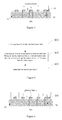
- Essence of the super-junction theory is the charge balance principle or the charge complementary principle, where a traditional low-doped withstand voltage structure is replaced with alternately arranged p-n structures (as shown in
Figure 1 ). - A traditional process for manufacturing a super-junction is an ion implantation process or a grooving and filling process. The ion implantation process mainly adopts a high energy ion implantation process or a repeated epitaxy and implantation process. The grooving and filling process mainly adopts a deep reactive ion etching process, or a repeated epitaxy, grooving and filling process.
- Complexity in the above described methods for manufacturing a super-junction results in a high cost for manufacturing a super-junction.
- To address the above technical problem, a method for manufacturing a super-junction is provided according to embodiments of the present disclosure, in order to simplify a manufacturing process of a super-junction and reduce the manufacture cost.
- A method for manufacturing a super-junction is provided, which includes:
- providing a lightly doped substrate; forming a p-type heavily doped region within the lightly doped substrate through a transmutation doping process by taking a first mask with a pattern of the p-type heavily doped region; forming an n-type heavily doped region within the lightly doped substrate through a transmutation doping process by taking a second mask with a pattern of the n-type heavily doped region; and performing annealing treatment.
- Preferably, the lightly doped substrate may be made of silicon, silicon carbide, gallium arsenide, or indium antimonide. The forming a p-type heavily doped region within the lightly doped substrate through a transmutation doping process may include: forming a high-energy photon beam by using a photon source; and forming a p-type heavily doped region within the lightly doped substrate by a nuclear reaction started by particle radiation on the lightly doped substrate by using the high-energy photon beam. The photon source may be an electronic linear accelerator photon source. The energy of the high-energy photon beam may range from 17.5 MeV to 22.5 MeV. The first mask may be made of high-energy photon absorber. The forming an n-type heavily doped region within the lightly doped substrate through a transmutation doping process may include: forming a neutron beam by using a neutron source; and forming an n-type heavily doped region within the lightly doped substrate by a nuclear reaction started by particle radiation on the lightly doped substrate by using the neutron beam. The neutron source may be a radioisotope neutron source, an accelerator neutron source, or a reactor neutron source. The second mask may be made of neutron absorber.
- A method for manufacturing a super-junction is provided, which includes:
- providing a first-type heavily doped substrate; forming a second-type heavily doped region within the first-type heavily doped substrate through a transmutation doping process by taking a third mask with a pattern of the second-type heavily doped region, wherein a region except for the second-type heavily doped region is a first-type heavily doped region; and performing annealing treatment.
- Preferably, the first-type heavily doped substrate may be a p-type heavily doped substrate, and the second second-type heavily doped region may be an n-type heavily doped region. The first-type heavily doped substrate may be made of silicon, silicon carbide, gallium arsenide, or indium antimonide. The forming a second-type heavily doped region within the first-type heavily doped substrate through a transmutation doping process may include: forming a neutron beam by using a neutron source; and forming a second-type heavily doped region within the first-type heavily doped substrate by a nuclear reaction started by particle radiation on the first-type heavily doped substrate by using the neutron beam to ignite.
- Preferably, the first-type heavily doped substrate may be an n-type heavily doped substrate, and the second-type heavily doped region may be a p-type heavily doped region. The first-type heavily doped substrate may be made of silicon, silicon carbide, diamond, germanium, gallium arsenide, or indium antimonide. The forming a second-type heavily doped region within the first-type heavily doped substrate through a transmutation doping process may include: forming a high-energy photon beam by using a photon source; and forming a second-type heavily doped region within the first-type heavily doped substrate by a nuclear reaction started by particle radiation on the first-type heavily doped substrate by using the high-energy photon beam.
- Preferably, the first-type heavily doped substrate may be made of germanium. The forming a second-type heavily doped region within the first-type heavily doped substrate through a transmutation doping process may include: forming a neutron beam by using a neutron source; and forming a second-type heavily doped region within the first-type heavily doped substrate by a nuclear reaction started by particle radiation on the first-type heavily doped substrate by using the neutron beam.
- A super-junction manufactured by any one of the methods described above is provided.
- A super-junction semiconductor device is provided, where a super-junction in the super-junction semiconductor device is the super-junction described above.
- The technical solution described above has the following advantages over the prior art.
- In the technical solutions according to the embodiments of the present disclosure, a p-type heavily doped region and an n-type heavily doped region are formed within a lightly doped substrate through a transmutation doping process. Or, a second-type heavily doped region is formed within the first-type heavily doped substrate through a transmutation doping process. In the transmutation doping process, a doped region within a substrate is obtained by a nuclear reaction, i.e., a super-junction can be obtained by only particle radiation and annealing treatment. While a super-junction in the prior art is obtained by a repeated epitaxy and implantation process or a repeated epitaxy, grooving and filling process. Therefore, in comparison with the prior art, the manufacturing process is simplified and the manufacture cost is reduced with the method for manufacturing a super-junction provided in the present disclosure.
-
-
Figure 1 is a schematic diagram of an existing super-junction; -
Figure 2 is a schematic flowchart of a method for manufacturing a super-junction according to an embodiment of the present disclosure; -
Figure 3 andFigure 4 are each a schematic flowchart of a doping process for a super-junction according to another embodiment of the present disclosure; -
Figure 5 is a schematic flowchart of another method for manufacturing a super-junction according to another embodiment of the present disclosure; and -
Figure 6 is a schematic flowchart of a doping process for a super-junction according to yet another embodiment of the present disclosure. - For clarity of the above objects, features and advantages of the disclosure, the embodiments of the disclosure will be described in detail in conjunction with the drawings.
- To facilitate sufficient understanding of the disclosure, details are explained in the following descriptions. However the present disclosure may be implemented in other ways different from those described herein, and similar extensions can be made by those skilled in the art without deviating from the essence of the present disclosure. Therefore the present disclosure is not limited to the embodiments described hereinafter.
- A method for manufacturing a super-junction is disclosed in this embodiment, as shown in
Figure 2 . The method includes the following steps S11 to S14. - In step S11, a lightly doped substrate is provided. The lightly doped substrate is an n-type lightly doped substrate, a p-type lightly doped substrate, or a lightly doped substrate close to an intrinsic semiconductor. The lightly doped substrate is made of material for manufacturing a semiconductor device, such as silicon, silicon carbide, gallium arsenide, indium antimonide.
- In step S12, a p-type heavily doped region is formed within the lightly doped substrate through a transmutation doping process by taking a first mask with a pattern of the p-type heavily doped region.
- In step S13, an n-type heavily doped region is formed within the lightly doped substrate through a transmutation doping process by taking a second mask with a pattern of the n-type heavily doped region.
- The p-type heavily doped region and the n-type heavily doped region are arranged alternately within the lightly doped substrate. Front surfaces of the p-type heavily doped region and the n-type heavily doped region are aligned with a front surface of the lightly doped substrate, and back surfaces of the p-type heavily doped region and the n-type heavily doped region are aligned with a back surface of the lightly doped substrate.
- In step S14, annealing treatment is performed to restore electrical properties of the lightly doped substrate. The temperature for the annealing treatment ranges from 800 Celsius degree to 900 Celsius degree.
- In the transmutation doping process, a doped region within a substrate is obtained by a nuclear reaction, i.e., a super-junction can be obtained by only particle radiation and annealing treatment. While a super-junction in the prior art is obtained by a repeated epitaxy and implantation process or a repeated epitaxy, grooving and filling process. Therefore, in comparison with the prior art, the manufacturing process is simplified and the manufacture cost is reduced with the method for manufacturing a super-junction provided in the present disclosure.
- Furthermore, the particle beam adopted in the transmutation doping process has strong penetrability, and can be applied to a thick substrate. Therefore, the super-junction formed by the method according to this embodiment is applicable to various semiconductor devices with various withstand voltages. In addition, a path of the particles in the lightly doped substrate is almost a straight line, and thus almost uniform doping is formed in well-defined regions within the lightly doped substrate, and a doping concentration can be precisely controlled.
- It should be noted that, orders of step S12 and step S13 are interchangeable in this embodiment.
- Another method for manufacturing a super-junction is disclosed in this embodiment. The method includes the following steps S21 to S24.
- In step S21, a lightly doped substrate is provided. The lightly doped substrate is an n-type lightly doped substrate, a p-type lightly doped substrate, or a lightly doped substrate close to an intrinsic semiconductor. The lightly doped substrate is made of material for manufacturing a semiconductor device, such as silicon, silicon carbide, gallium arsenide, indium antimonide.
- In step S22, a p-type heavily doped region is formed within the lightly doped substrate. Step S22 includes the following steps S221 and S222.
- In step S221, a high-energy photon beam is formed by using a photon source.
- Since the high-energy photon beam may be generated by bremsstrahlung from an electronic linear accelerator, the photon source in this embodiment is preferably an electronic linear accelerator photon source. And the energy of the generated high-energy photon beam is between 17.5 MeV and 22.5 MeV.
- In order to achieve local doping, the photons in the photon beam generated by the photon source need to move in directions parallel to each other. That is, the photon beam is similar to parallel light, or the photon beam has at least certain parallelism.
- In step S222, a p-type heavily doped region is formed within the lightly doped substrate by a nuclear reaction started by particle radiation on the lightly doped substrate by using the neutron beam.
- In the method described above, the material is doped by photon radiation.
- An attenuation coefficient of high-energy electrons in silicon is very small, so it is possible to achieve deep doping in semiconductor. And the distribution of isotopic atoms in the crystal is very uniform, and thus very uniform doping is formed through transmutation of an element beam, by particle radiation on the lightly doped substrate by using the high-energy photon.
- Furthermore, as for the lightly doped substrate made of silicon, a p-type impurity may be formed by a nuclear reaction started by the radiation of the high-energy photon beam.
- That is, silicon-30 is transmuted into aluminum-27 and releases one proton after absorbing one photon, and specifically the nuclear reaction is:
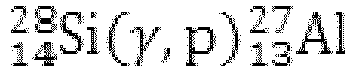
- Or, silicon-30 is transmuted into silicon-27 and releases one neutron after absorbing one photon, and then the silicon-27 is transmuted into aluminum-27 by releasing a positron after a half-life of 4.2s. The nuclear reaction is:

- The stable Al generated according to this reaction is just the donor element for p-doped silicon.
- Although a threshold value of photon energy for the nuclear reaction is 11.6 MeV, Huge resonance produces a maximum photon capture cross section when the photon energy is between 17.5 MeV and 22.5 MeV. Therefore, for example, photon energy in the high energy photon beam according to the present embodiment is between 17.5 MeV and 22.5MeV, preferably 20 MeV
- As for a lightly doped substrate made of silicon carbide, a p-type impurity may be formed by a nuclear reaction started by radiation of the high-energy photon beam on the lightly doped substrate.
- That is, after absorbing one photon, a carbon-12 is transmuted into a boron-11 and releases one proton, and the nuclear reaction is:

- Alternatively, a carbon-12 is transmuted into a carbon-11 and release one proton after absorbing one photon, and then the carbon-11 is transmuted into a boron-11 by releasing one positron. Specifically the nuclear reaction is:

- A nuclear reaction process of silicon in silicon carbide is the same as the reaction of the silicon described above.
- Furthermore, as for the lightly doped substrate made of gallium arsenide or indium antimonide, a p-type impurity may be formed by a nuclear reaction after the lightly doped substrate is radiated by the high-energy photon beam.
- Since in the particle irradiation process a local transmutation doping is achieved by using a high-energy photon beam, a first mask used for forming the p-type heavily doped region is made of photon absorber to block unwanted particle radiation.
- The high-energy photon absorber includes at least one of an elementary substance or compound of heavy metal, a titanate or silane coupling agent, and other substances capable of effectively absorbing photons.
- In step S23, an n-type heavily doped region is formed within the lightly doped substrate. Step S23 includes the following steps S231 and S232.
- In step S231, a neutron source is provided to form a neutron beam.
- A free neutron may decay into a proton and release an electron and an anti-electric neutrino because the free neutron is unstable, an average life of the free neutron is only 15 minutes, and thus it can't be stored for a long term. Therefore, an appropriate source for generating neutrons is required to supply neutrons. The neutron sources are classified into the following three types:
- 1st: Radioisotope neutron source. The radioisotope neutron source includes: a (α, n) neutron source, which is obtained by employing a nuclear reaction 9Be+α→12C+n+5.701 MeV by the following steps: 238Pu, 226Ra or 241Am irradiating α rays are mixed uniformly with a beryllium metal powder at a certain percentage, and then the mixture is pressed into a small cylinder and sealed in a metal case; and a (γ, n) neutron source, which generates neutrons by γ rays irradiated through a nuclear reaction, including a 24Na-Be source, a 124Sb-Be source and the like. The radioisotope neutron source can be simply manufactured into a smaller volume and can be used conveniently.
- 2nd: Accelerator neutron source. The accelerator neutron source generates neutrons through a nuclear reaction by using charged particles accelerated by the accelerator to bombard an appropriate target nucleus. The most common nuclear reactions include (d, n), (p, n), (γ, n), and the like. An neutron intensity generated by the accelerator neutron source is much larger than that of the radioisotope neutron source, and monoenergetic neutrons can be obtained in a wide energy range through the accelerator neutron source. Moreover, pulse neutrons may be obtained if the accelerator is pulse modulated.
- 3rd, Reactor neutron sources. The reactor neutron source generates lots of neutrons by using an atomic nucleus fission reactor. Reactor is the strongest thermal neutron source. Neutrons may be led out by opening a hole in a wall of the reactor, and the energy of the obtained neutrons is in continuous distribution, which is similar to Maxwell distribution. Neutron beams with various energies can be obtained by taking certain measures.
- Of course, like the requirement for the photon beam, the neutrons in the neutron beam also need to move in directions parallel to each other. The neutrons beam has at least certain parallelism.
- In step S232, an n-type heavily doped region is formed within the lightly doped substrate by a nuclear reaction started by particleradiation on the lightly doped substrate with the neutron beam.
- In the method described above, the material is doped by neutron radiation. The distribution of isotopic atoms in the crystal is very uniform and a penetration depth of the neutron in a semiconductor is very large (about 100 cm), and thus very uniform doping is formed through transmutation of the element by particle radiation on the lightly doped substrate with the neutron beam. This is very useful for the manufacture of a high-power semiconductor device and a radiation detecting device.
- In addition, as for the lightly doped substrate made of silicon, an n-type impurity may be formed by a nuclear reaction started after the lightly doped substrate is radiated by the neutron beam. That is, after absorbing one neutron, a silicon-30 is transmuted into a silicon-31 and releases one photon, and then after a half-life of 2.6 h, the silicon-31 is transmuted into a phosphorus-31 by releasing an electron. The nuclear reaction is:

- The stable P generated by the reaction is just the donor element for n-type doped silicon.
- The concentration ND (in cm-3) of P achieved after the radiation is performed can be calculated using the following formula:

- Where, NSi30 (in cm-3) is abundance of 30Si; σ is a radiative capture cross section of a Si atom with respect to a thermal neutron (σ =0.11 barn); ψ (in cm-2s-1) is a radiation dose of thermal neutrons , and t (in s) is radiation time duration.
- Since the abundance of 30Si, NSi30, is constant in a lightly doped substrate, and the radiative capture cross section σ of a Si atom with respect to a thermal neutron is also constant, the doped impurity concentration in the n-type silicon can be precisely controlled by adjusting the radiation dose ψ of thermal neutrons and the radiation time duration t. Moreover, only one element (P) is generated in the reaction above, and no compensation due to transmutation occures.
- In addition, 30Si has a natural uniform distribution in silicon, and thus 31P generated through transmutation is also in a uniform distribution, i.e., the impurity in the N-type silicon is in a uniform distribution.
- In addition, to avoid the influence of an ununiform distribution of the neutron beam flux, a metal flux homogenizer can be used to obtain a uniform distribution of the neutron beam flux.
- As for a lightly doped substrate made of silicon carbide, like the lightly doped substrate made of silicon, when the lightly doped substrate is radiated with a neutron beam, after absorbing one neutron, a silicon-30 is transmuted into a silicon-31 and releases one photon, and after a half-life of 2.6h, the silicon-31 is transmuted into a phosphorus-31 by releasing a electron. Therefore the donor element phosphorus appears in the silicon carbide, and thus the silicon carbide becomes n-type doped silicon carbide.
- In addition, as for a lightly doped substrate made of gallium arsenide or indium antimonide, when being radiated with a neutron beam, an n-type impurity can be generated by a nuclear reaction.
- Because the particle radiation process described above achieves a local transmutation doping using the neutron beam, a second mask for forming an n-type heavily doped region is made of neutron absorber to block the unwanted particle radiation.
- Effective neutron absorber is a radioisotope capable of generating a stable atom nucleus by absorbing one neutron. For example, a xenon-135 (a half-life of is about 9.1 hours) can be transmuted into a stable xenon-136 by absorbing one neutron. In a nuclear reactor by nuclear fissions of uranium-235, uranium-233 and plutonium-239, and the iodine-135 can generate xenon-135 by decaying rapidly and releasing a β particle (a high energy electron). Therefore, the neutron absorber may be at least one of the above isotopes.
- Other neutron absorber mainly includes: helium-3 isotope, which can generate a tritium (a heavy isotope of hydrogen) after absorbing a neutron; boron-10, which can generate a lithium and a helium nucleus after absorbing a neutron; and samarium-149, which is also effective neutron absorber and can generate a stable samarium-150 isotopes after absorbing a neutron.
- In addition, some neutron absorbers used for control rods in nuclear reactors include cadmium, hafnium and rare earth metal gadolinium. These neutron absorbers contain several isotopes, and some are very effective neutron absorber.
- All these materials described above may be used as neutron absorbers in this embodiment, i.e., can be used for making the second mask. Furthermore, the second mask made of a selected suitable material and having sufficient thickness can effectively absorb neutrons to function as a mask and to achieve local doping.
- In addition, for ease of understanding,
Figure 3 andFigure 4 each shows a doping process described above. - As shown in
Figure 3 , a lightly dopedsubstrate 101 is covered with afirst mask 102 with a pattern of the p-type heavily doped region, and thefirst mask 102 and the lightly dopedsubstrate 101 are aligned with each other. After that, the lightly dopedsubstrate 101 is radiated with a high-energy photon beam in an incident direction perpendicular to a surface of the lightly dopedsubstrate 101. In a position sheltered by thefirst mask 102, the high-energy photon beam is absorbed by thefirst mask 102. While in a position of the lightly dopedsubstrate 101 unsheltered by thefirst mask 102, the high-energy photon beam can be injected directly into the lightly dopedsubstrate 101 and starts a nuclear reaction (for example, silicon is transmuted into aluminum), to obtain a p-type heavily dopedregion 10. - As shown in
Figure 4 , a lightly dopedsubstrate 101 is covered and aligned with asecond mask 103 with a pattern of the n-type heavily doped region. After that, the lightly dopedsubstrate 101 is radiated with a neutron beam in an incident direction perpendicular to a surface of the lightly dopedsubstrate 101. In a position of the lightly dopedsubstrate 101 sheltered by thesecond mask 103, the neutron beam is absorbed by thesecond mask 103. While in a position of the lightly dopedsubstrate 101 unsheltered by thesecond mask 103, the neutron beam can be injected directly into the lightly dopedsubstrate 101 and starts a nuclear reaction (for example, silicon is transmuted into phosphor), to obtain an n-type heavily dopedregion 11. - The p-type heavily doped
region 10 and the n-type heavily dopedregion 11 are arranged alternately within the lightly dopedsubstrate 101. Front surfaces of the p-type heavily dopedregion 10 and the n-type heavily dopedregion 11 are aligned with a front surface of the lightly dopedsubstrate 101, and back surfaces of the p-type heavily dopedregion 10 and the n-type heavily dopedregion 11 are aligned with a back surface of the lightly dopedsubstrate 101. - In step S24, annealing treatment is performed.
- Defects may be caused in the lightly doped substrate by the radiation in the above-described method, and the lightly doped substrate significantly changes in physical properties. Thus, a annealing treatment on the lightly doped substrate is required in order to restore electrical properties of the lightly doped substrate, wherein the annealing temperature ranges preferably from 800 Celsius degree to 900 Celsius degree.
- In the technical solutions according to the embodiment of the present disclosure, a p-type heavily doped region and an n-type heavily doped region are formed within the lightly doped substrate through a transmutation doping process. In the transmutation doping process, a doped region within a substrate is obtained by a nuclear reaction, i.e., a super-junction can be obtained by only particle radiation and annealing treatment. While a super-junction in the prior art is obtained by a repeated epitaxy and implantation process or a repeated epitaxy, grooving and filling process. Therefore, in comparison with the prior art, the manufacturing process is simplified and the manufacture cost is reduced with the method for manufacturing a super-junction provided in the present disclosure.
- Furthermore, particles adopted in the transmutation doping process have strong penetrability, and thus the transmutation doping process may be applied to a thick substrate. The super-junction formed by the method according to this embodiment is applicable to various semiconductor devices with various withstand voltages. In addition, the path of the particles in the lightly doped substrate is almost a straight line, and thus almost a uniform distribution is formed in a well-defined doping region within the lightly doped substrate, and a doping concentration can be precisely controlled.
- It should be noted that, the orders of step S22 and step S23 are interchangeable in this embodiment.
- Still another method for manufacturing a super-junction is disclosed in this embodiment. As shown in
Figure 5 , the method includes the following steps S31 to S33. - In step S31, a first-type heavily doped substrate is provided. The first-type heavily doped substrate is an n-type heavily doped substrate or a p-type heavily doped substrate.
- In step S32, by taking a third mask with a pattern of the second-type heavily doped region, a second-type heavily doped region is formed within the first-type heavily doped substrate through a transmutation doping process, where a region other than the second-type heavily doped region is a first-type heavily doped region.
- Specifically, the first-type heavily doped region and the second-type heavily doped region are arranged alternately.
- In step S33, annealing treatment is performed to restore electrical properties of the first-type heavily doped substrate. The temperature for the annealing treatment is between 800 Celsius degree to 900 Celsius degree.
- In this embodiment, the second-type heavily doped region is formed within the first-type heavily doped substrate through a transmutation doping process. In the transmutation doping process, a doped region within a substrate is obtained by a nuclear reaction, i.e., a super-junction can be obtained by only particle radiation and annealing treatment. While a super-junction in the prior art is obtained by a repeated epitaxy and implantation process or a repeated epitaxy, grooving and filling process. Therefore, in comparison with the prior art, the manufacturing process is simplified and the manufacture cost is reduced with the method for manufacturing a super-junction provided in the present disclosure.
- Furthermore, particles adopted in the transmutation doping process have strong penetrability, and thus the transmutation doping process may be applied to a thick substrate. and the super-junction formed by the method according to this embodiment is applicable to various semiconductor devices with various withstand voltages. In addition, the path of the particles in the lightly doped substrate is almost a straight line, and thus almost a uniform distribution is formed in a well-defined doping region within the lightly doped substrate, and a doping concentration can be precisely controlled.
- In addition, as compared with the previous embodiments, the method for manufacturing a super-junction according to this embodiment is further simplified and the manufacture cost is further reduced.
- Still another method for manufacturing a super-junction is disclosed in this embodiment. The method includes the following steps S41 to S43.
- In step S41, a first-type heavily doped substrate is provided. The first-type heavily doped substrate is a p-type heavily doped substrate. The first-type heavily doped substrate is made of material for manufacturing a semiconductor device, such as silicon, silicon carbide, gallium arsenide, indium antimonide which can be used for manufacturing a semiconductor device.
- In step S42, a second-type heavily doped region is formed within the first-type heavily doped substrate, wherein a region other than the second-type heavily doped region is a first-type heavily doped region. The second-type heavily doped region is an n-type heavily doped region. Since the first-type heavily doped region is of the same type as the first-type heavily doped substrate, the first-type heavily doped region is a p-type heavily doped region.
- Step S42 includes the following steps S421 and S422.
- In step S421, a neutron source is provided to form a neutron beam.
- In step S422, n-type impurity is formed within the first-type heavily doped substrate a nuclear reaction started by particle radiation on the first-type heavily doped substrate with the neutron beam, so as to obtain a second-type heavily doped region.
- In the method described above, since a local transmutation doping is performed on the material by using neutron radiation, a third mask with a pattern of the second-type heavily doped region is required, and the third mask is made of neutron absorber.
- In step S43, annealing treatment is performed to restore electrical properties of the first-type heavily doped substrate. The temperature for the annealing treatment is between 800 Celsius degree and 900 Celsius degree.
- Yet another method for manufacturing a super-junction is disclosed in this embodiment. The method includes the following steps S51 to S53.
- In step S51, a first-type heavily doped substrate is provided. The first-type heavily doped substrate is an n-type heavily doped substrate. The first-type heavily doped substrate is made of material such as silicon, silicon carbide, diamond, germanium, gallium arsenide, indium antimonide, which can be used for manufacturing a semiconductor device.
- In step S52, a second-type heavily doped region is formed within the first-type heavily doped substrate, wherein a region other than the second-type heavily doped region is a first-type heavily doped region. The second-type heavily doped region is a p-type heavily doped region. Since the first-type heavily doped region has the same type as the first-type heavily doped substrate, the first-type heavily doped region is an n-type heavily doped region.
- Step S52 includes the following steps S521 and S522.
- In step S521, a photon source is provided to form a high-energy photon beam.
- In step S522, a p-type impurity is formed within the first-type heavily doped substrate by a nuclear reaction started by particle radiation on the first-type heavily doped substrate with the high-energy photon beam, so as to obtain a second-type heavily doped region.
- As for the first-type heavily doped substrate made of diamond, a p-type impurity may also be formed by a nuclear reaction after the first-type heavily doped substrate is irradiated by the high-energy photon beam.
- That is, after absorbing one photon, a carbon-12 is transmuted into a boron-11 and release one proton , and the nuclear reaction is:

- Or, after absorbing one photon, a carbon-12 is transmuted into a carbon-11 and releases one proton, and then the carbon-11 is transmuted into a boron-11 by releasing one positron. The nuclear reaction is:

- In the method described above, since a local transmutation doping is performed on the material by using photon irradiation, a third mask with a pattern of the second-type heavily doped region is required, and the third mask is made of a high-energy photon absorber.
- For ease of understanding,
Figures 6 shows a doping process described above. - A first-type heavily doped
substrate 201 is covered and aligned with athird mask 202 with a pattern of the second-type heavily doped region. After that, the first-type heavily dopedsubstrate 201 is radiated with a high-energy photon beam in an incident direction perpendicular to a surface of the first-type heavily dopedsubstrate 201. In a position of the first-type heavily dopedsubstrate 201 sheltered by thethird mask 202, the high-energy photon beam is absorbed by thethird mask 202. While in a position of the first-type heavily dopedsubstrate 201 unsheltered by thethird mask 202, the high-energy photon beam can be injected directly into the first-type heavily dopedsubstrate 201 and starts a nuclear reaction (for example, a carbon is transmuted into a boron), to obtain a second-type heavily dopedregion 21. A region other than the second-type heavily dopedregion 21 is a first-type heavily dopedregion 20. - In step S53, annealing treatment is performed to restore electrical properties of the first-type heavily doped substrate. The temperature for the annealing treatment is between 800 Celsius degree and 900 Celsius degree.
- Still yet another method for manufacturing a super-junction is disclosed in this embodiment. The method includes the following steps S61 to S63.
- In step S61, a first-type heavily doped substrate is provided. The first-type heavily doped substrate is an n-type heavily doped substrate and made of a germanium.
- In step S62, a second-type heavily doped region is formed within the first-type heavily doped substrate, wherein a region other than the second-type heavily doped region is a first-type heavily doped region. The second-type heavily doped region is a p-type heavily doped region. Since the first-type heavily doped region is of the same type as the first-type heavily doped substrate, the first-type heavily doped region is an n-type heavily doped region.
- Step S62 includes the following steps S621 and S622.
- In step S621, a neutron source is provided to form a neutron beam.
- In step S622, a p-type impurity is formed within the first-type heavily doped substrate a nuclear reaction started by particle radiation on the first-type heavily doped substrate with the neutron beam, so as to obtain a second-type heavily doped region.
- In the method described above, since a local transmutation doping is performed on the material by using neutron radiation, a third mask with a pattern of the second-type heavily doped region is required, and the third mask is made of a neutron absorber.
- In step S63, annealing treatment is performed to restore electrical properties of the first-type heavily doped substrate. The temperature for the annealing treatment is between 800 Celsius degree to 900 Celsius degree.
- A super-junction is disclosed in this embodiment, which is formed by the method according to any one of the above described embodiments, i.e., the super-junction is formed by a transmutation doping process.
- Therefore, the super-junction formed by the method according to this embodiment is applicable to various semiconductor devices with various withstand voltages. Thus the doping region of the super junction is well defined, the doping concentration can be precisely controlled, and the doping is in a uniform distribution.
- A super-junction semiconductor device is disclosed in this embodiment, wherein a super-junction in the super-junction semiconductor device is the super-junction disclosed by the previous embodiment.
- The super-junction may be achieved between the manufacture processes of other structures of the super-junction semiconductor device, so that the super-junction and other structures of the super-junction semiconductor device can share an annealing process. The manufacturing process of the super-junction semiconductor device is further simplified and the manufacture cost is further reduced.
- Taking a method for manufacturing a super-junction IGBT (Insulated Gate Bipolar Transistor) as an example, the method includes the following steps:
- providing a heavily doped substrate;
- growing epitaxially a first-type heavily doped layer on a surface of the heavily doped substrate;
- forming a second-type heavily doped region within the first-type heavily doped layer through a transmutation doping process by taking a third mask with a pattern of the second-type heavily doped region, wherein a region other than the second-type heavily doped region is a first-type heavily doped region, and the first-type heavily doped region and the second-type heavily doped region are arranged alternately;
- forming a front surface structure including a trap region, an emitter region, a gate, and front metal on the first-type heavily doped layer on which the first-type heavily doped region and the second-type heavily doped region are formed, to accomplish the manufacture of the front surface structure of the super-junction IGBT;
- performing annealing treatment to restore electrical properties of the first-type heavily doped layer and to activating the doped ions in the structures such as the trap region and the emitter region, where the temperature for the annealing treatment is between 800 Celsius degree and 900 Celsius degree; and
- forming a collector region and back metal on a back surface of the heavily doped substrate to accomplish the manufacture of the back surface structure of the super-junction IGBT.
- In addition, the super-junction semiconductor device may also be a semiconductor device having a super-junction VDMOS, a super-junction PIN, or the like.
- It should be noted that other charged particles or uncharged particles may also be used as the particles for the radiation in the embodiments of the present disclosure, as long as the transmutation doping can be achieved. And the radiation energy of the particles is at least able to start a nuclear reaction, and the radiation dose may be pre-calculated as desired. As for other semiconductor materials and the radiation particles, a super-junction may be formed by this method as long as corresponding doping types can be formed. And the formed super-junction may also be used for various semiconductor devices, which are not listed out here.
- In addition, a shorter duration is required for some materials and particles than a duration required in a conventional diffusion process. Therefore, the method for manufacturing a super-junction provided by the disclosure may further improve the production efficiency.
- In addition, it should be noted that since the nuclear transmutation doping of the semiconductor results in residual radioactivity. Therefore, the lightly doped substrate and the heavily doped substrate requires radiation cooling for a certain duration after the particle radiation, and then can be regarded as a non-radioactive material for subsequent operations.
- Drawings in the description are schematic diagrams, and do not represent a real scale. The embodiments of the present disclosure are described herein in a progressive manner, with emphasis on the difference between the embodiments,; hence, for the same or similar parts between the embodiments, one can refer to other embodiments.
- The above description of the disclosed embodiments enables those skilled in the art to implement or utilize the present disclosure. It will be obvious for those skilled in the art to modify the embodiments in various ways. The general principles defined herein can be implemented in other embodiments without departing from the spirit and the scope of the present disclosure. Therefore, the present disclosure is not limited to these embodiments shown herein, but conforms to the broadest scope consistent with the principles and the novelty features disclosed herein.
Claims (29)
- A method for manufacturing a super-junction, comprising:providing a lightly doped substrate;forming a p-type heavily doped region within the lightly doped substrate through a transmutation doping process by taking a first mask with a pattern of the p-type heavily doped region;forming an n-type heavily doped region within the lightly doped substrate through a transmutation doping process by taking a second mask with a pattern of the n-type heavily doped region pattern; andperforming annealing treatment.
- The method according to claim 1, wherein the lightly doped substrate is made of silicon, silicon carbide, a gallium arsenide, or an indium antimonide.
- The method according to claim 2, wherein the forming a p-type heavily doped region within the lightly doped substrate through a transmutation doping process comprises:forming a high-energy photon beam by using a photon source; andforming a p-type heavily doped region within the lightly doped substrate by a nuclear reaction started by particle radiation on the lightly doped substrate by using the high-energy photon beam.
- The method according to claim 3, wherein the photon source is an electronic linear accelerator photon source.
- The method according to claim 3, wherein the energy of the high-energy photon beam is between 17.5 MeV and 22.5 MeV.
- The method according to claim 3, wherein photons in the high-energy photon beam move in directions parallel to each other.
- The method according to claim 3, wherein the first mask is made of high-energy photon absorber.
- The method according to claim 7, wherein the high-energy photon absorber comprises at least one of an elementary substance or a compound of heavy metal, and a titanate or silane coupling agent.
- The method according to claim 2, wherein the forming an n-type heavily doped region within the lightly doped substrate through a transmutation doping process comprises:forming a neutron beam by using a neutron source; andforming an n-type heavily doped region within the lightly doped substrate by a nuclear reaction started by particle radiation on the lightly doped substrate by using the neutron beam.
- The method according to claim 9, wherein the neutron source is a radioisotope neutron source, an accelerator neutron source, or a reactor neutron source.
- The method according to claim 9, wherein the neutrons in the neutron beam move in directions parallel to each other.
- The method according to claim 9, wherein the second mask is made of neutron absorber.
- The method according to claim 12, wherein the neutron absorber comprises at least one of xenon-135, a helium-3 isotope, a boron-10, or a samarium-149.
- A method for manufacturing a super-junction, comprising:providing a first-type heavily doped substrate;forming a second-type heavily doped region within the first-type heavily doped substrate through a transmutation doping process by taking a third mask with a pattern of the second-type heavily doped region, wherein a region except for the second-type heavily doped region is a first-type heavily doped region; andperforming annealing treatment.
- The method according to claim 14, wherein the first-type heavily doped substrate is a p-type heavily doped substrate, and the second-type heavily doped region is an n-type heavily doped region.
- The method according to claim 15, wherein the first-type heavily doped substrate is made of silicon, silicon carbide, gallium arsenide, or indium antimonide.
- The method according to claim 16, wherein the forming a second-type heavily doped region within the first-type heavily doped substrate through a transmutation doping process comprises:forming a neutron beam by using a neutron source; andforming a second-type heavily doped region within the first-type heavily doped substrate by a nuclear reaction started by particle radiation on the first-type heavily doped substrate by using the neutron beam to ignite.
- The method according to claim 17, wherein the third mask is made of a neutron absorber.
- The method according to claim 14, wherein the first-type heavily doped substrate is an n-type heavily doped substrate, and the second heavily doped region is a p-type heavily doped region.
- The method according to claim 19, wherein the first-type heavily doped substrate is made of silicon, silicon carbide, diamond, germanium, gallium arsenide, or indium antimonide.
- The method according to claim 20, wherein the forming a second-type heavily doped region within the first-type heavily doped substrate through a transmutation doping process comprises:forming a high-energy photon beam by using a photon source; andforming a second-type heavily doped region within the first-type heavily doped substrate by a nuclear reaction started by particle radiation on the first-type heavily doped substrate by using the high-energy photon beam.
- The method according to claim 21, wherein the third mask is made of high-energy photon absorber.
- The method according to claim 19, wherein the first-type heavily doped substrate is made of germanium.
- The method according to claim 23, wherein the forming a second-type heavily doped region within the first-type heavily doped substrate through a transmutation doping process comprises:forming a neutron beam by using a neutron source; andforming a second-type heavily doped region within the first-type heavily doped substrate by a nuclear reaction started by particle radiation on the first-type heavily doped substrate by using the neutron beam.
- The method according to claim 24, wherein the third mask is made of neutron absorber.
- The method according to claim 1 or 14, wherein the temperature for the annealing treatment ranges from 800 Celsius degree to 900 Celsius degree.
- A super-junction manufactured by the method according to claim 1 or 14.
- A super-junction semiconductor device, wherein a super-junction in the super-junction semiconductor device is the super-junction according to claim 27.
- The super-junction semiconductor device according to claim 28, wherein the super-junction semiconductor device is a super-junction IGBT, a super-junction VDMOS, or a super-junction PIN.
Applications Claiming Priority (1)
| Application Number | Priority Date | Filing Date | Title |
|---|---|---|---|
| PCT/CN2012/085993 WO2014086010A1 (en) | 2012-12-06 | 2012-12-06 | Super-junction manufacturing method |
Publications (3)
| Publication Number | Publication Date |
|---|---|
| EP2930739A1 true EP2930739A1 (en) | 2015-10-14 |
| EP2930739A4 EP2930739A4 (en) | 2016-08-24 |
| EP2930739B1 EP2930739B1 (en) | 2020-07-01 |
Family
ID=50882769
Family Applications (1)
| Application Number | Title | Priority Date | Filing Date |
|---|---|---|---|
| EP12889660.2A Active EP2930739B1 (en) | 2012-12-06 | 2012-12-06 | Super-junction manufacturing method |
Country Status (2)
| Country | Link |
|---|---|
| EP (1) | EP2930739B1 (en) |
| WO (1) | WO2014086010A1 (en) |
Family Cites Families (10)
| Publication number | Priority date | Publication date | Assignee | Title |
|---|---|---|---|---|
| US3255050A (en) * | 1962-03-23 | 1966-06-07 | Carl N Klahr | Fabrication of semiconductor devices by transmutation doping |
| US4135951A (en) * | 1977-06-13 | 1979-01-23 | Monsanto Company | Annealing method to increase minority carrier life-time for neutron transmutation doped semiconductor materials |
| DE3714357C2 (en) * | 1986-04-30 | 1994-02-03 | Toshiba Ceramics Co | Silicon wafer and method of manufacturing the same, and silicon wafer selector |
| CH670332A5 (en) * | 1986-09-17 | 1989-05-31 | Bbc Brown Boveri & Cie | |
| CN1010038B (en) * | 1988-03-26 | 1990-10-17 | 河北工学院 | Annealing process for neutron transmutation doping Czochralski silicon |
| GB9916370D0 (en) * | 1999-07-14 | 1999-09-15 | Koninkl Philips Electronics Nv | Manufacture of semiconductor devices and material |
| US6475864B1 (en) * | 1999-10-21 | 2002-11-05 | Fuji Electric Co., Ltd. | Method of manufacturing a super-junction semiconductor device with an conductivity type layer |
| WO2002067333A1 (en) * | 2001-02-21 | 2002-08-29 | Mitsubishi Denki Kabushiki Kaisha | Semiconductor device and method of manufacturing the same |
| US6974720B2 (en) * | 2003-10-16 | 2005-12-13 | Cree, Inc. | Methods of forming power semiconductor devices using boule-grown silicon carbide drift layers and power semiconductor devices formed thereby |
| CN102254828A (en) * | 2011-07-18 | 2011-11-23 | 无锡新洁能功率半导体有限公司 | Method for making semiconductor device with super junction structure and rapid reverse recovery characteristic |
-
2012
- 2012-12-06 EP EP12889660.2A patent/EP2930739B1/en active Active
- 2012-12-06 WO PCT/CN2012/085993 patent/WO2014086010A1/en not_active Ceased
Also Published As
| Publication number | Publication date |
|---|---|
| EP2930739A4 (en) | 2016-08-24 |
| WO2014086010A1 (en) | 2014-06-12 |
| EP2930739B1 (en) | 2020-07-01 |
Similar Documents
| Publication | Publication Date | Title |
|---|---|---|
| Markov | On high energy neutrino physics | |
| Uesaka et al. | Compact neutron sources for energy and security | |
| Rahastama et al. | Optimization of surface passivation parameters in [147Pm]-Si planar pn junction betavoltaic based on analytical 1-D minority carrier diffusion equation approaches | |
| CN103854999A (en) | Super junction manufacturing method | |
| EP2930739B1 (en) | Super-junction manufacturing method | |
| CN103855000A (en) | Fabrication method of reverse-resistance type insulated gate bipolar transistor | |
| US20250253067A1 (en) | Semiconductor betavoltaic battery with integrated beta emitter | |
| Heydari et al. | Optimization study to determine the appropriate location for the implementation of silicon doping in Tehran research reactor | |
| Franchoo | The alto tandem and isol facility at IPN orsay | |
| Kamh et al. | Environmental conditions effect on characteristics of some unijunction and bijunction semiconductor devices | |
| WO2014086011A1 (en) | Rb-igbt manufacturing method | |
| Craddock et al. | Basic and applied research at the TRIUMF meson factory | |
| Wang et al. | Proton–boron fusion in femtosecond-laser-irradiated nanowire array target | |
| DeRosa et al. | Radiation characterization and mitigation of high-energy H+ beams: P. DeRosa et al. | |
| US20250194194A1 (en) | Radiation doped semiconductor junctions | |
| Liu et al. | Energy deposition, parameter optimization, and performance analysis of space radiation voltaic batteries | |
| Tunkl | Development of a new runaway electron diagnostics method based on strip semiconductor detectors | |
| Álvarez Frau | Characterization of scintillator materials for next generation fusion devices | |
| Maekawa et al. | Development of 44Sc high spin-polarized positron source using high energy proton beam | |
| Araujo et al. | LETTER OF INTENT TO THE ISOLDE AND NEUTRON TIME-OF-FLIGHT COMMITTEE (INTC) | |
| Nakai et al. | Industrial applications of laser neutron source | |
| Amouroux et al. | Measurement of mass yields from the 241Am (2nth, f) reaction at the Lohengrin Spectrometer | |
| US20200402802A1 (en) | Photonuclear transmutation doping in gallium-based semiconductor materials | |
| Skobelev et al. | Investigating the nuclear fusion and nucleon transfer channels in the 197Au+ 6He reaction at 6He energies up to 20 MeV/A | |
| Tripathi | Study of Sic-Based Neutron Detector for Applications in The Harsh Environment of Fast Reactors |
Legal Events
| Date | Code | Title | Description |
|---|---|---|---|
| PUAI | Public reference made under article 153(3) epc to a published international application that has entered the european phase |
Free format text: ORIGINAL CODE: 0009012 |
|
| 17P | Request for examination filed |
Effective date: 20150706 |
|
| AK | Designated contracting states |
Kind code of ref document: A1 Designated state(s): AL AT BE BG CH CY CZ DE DK EE ES FI FR GB GR HR HU IE IS IT LI LT LU LV MC MK MT NL NO PL PT RO RS SE SI SK SM TR |
|
| AX | Request for extension of the european patent |
Extension state: BA ME |
|
| DAX | Request for extension of the european patent (deleted) | ||
| RA4 | Supplementary search report drawn up and despatched (corrected) |
Effective date: 20160722 |
|
| RIC1 | Information provided on ipc code assigned before grant |
Ipc: H01L 21/263 20060101ALI20160718BHEP Ipc: H01L 21/261 20060101ALI20160718BHEP Ipc: H01L 21/336 20060101ALI20160718BHEP Ipc: H01L 29/06 20060101ALI20160718BHEP Ipc: H01L 21/00 20060101AFI20160718BHEP |
|
| RIC1 | Information provided on ipc code assigned before grant |
Ipc: H01L 21/261 20060101ALI20190917BHEP Ipc: H01L 21/263 20060101ALI20190917BHEP Ipc: H01L 29/739 20060101ALN20190917BHEP Ipc: H01L 21/336 20060101AFI20190917BHEP Ipc: H01L 29/868 20060101ALN20190917BHEP Ipc: H01L 29/78 20060101ALN20190917BHEP Ipc: H01L 29/06 20060101ALI20190917BHEP |
|
| REG | Reference to a national code |
Ref country code: DE Ref legal event code: R079 Ref document number: 602012071075 Country of ref document: DE Free format text: PREVIOUS MAIN CLASS: H01L0021000000 Ipc: H01L0021336000 |
|
| RIC1 | Information provided on ipc code assigned before grant |
Ipc: H01L 21/261 20060101ALI20191127BHEP Ipc: H01L 29/06 20060101ALI20191127BHEP Ipc: H01L 29/78 20060101ALN20191127BHEP Ipc: H01L 21/263 20060101ALI20191127BHEP Ipc: H01L 29/739 20060101ALN20191127BHEP Ipc: H01L 21/336 20060101AFI20191127BHEP Ipc: H01L 29/868 20060101ALN20191127BHEP |
|
| GRAP | Despatch of communication of intention to grant a patent |
Free format text: ORIGINAL CODE: EPIDOSNIGR1 |
|
| STAA | Information on the status of an ep patent application or granted ep patent |
Free format text: STATUS: GRANT OF PATENT IS INTENDED |
|
| INTG | Intention to grant announced |
Effective date: 20200124 |
|
| GRAS | Grant fee paid |
Free format text: ORIGINAL CODE: EPIDOSNIGR3 |
|
| GRAA | (expected) grant |
Free format text: ORIGINAL CODE: 0009210 |
|
| STAA | Information on the status of an ep patent application or granted ep patent |
Free format text: STATUS: THE PATENT HAS BEEN GRANTED |
|
| AK | Designated contracting states |
Kind code of ref document: B1 Designated state(s): AL AT BE BG CH CY CZ DE DK EE ES FI FR GB GR HR HU IE IS IT LI LT LU LV MC MK MT NL NO PL PT RO RS SE SI SK SM TR |
|
| REG | Reference to a national code |
Ref country code: GB Ref legal event code: FG4D |
|
| REG | Reference to a national code |
Ref country code: AT Ref legal event code: REF Ref document number: 1286942 Country of ref document: AT Kind code of ref document: T Effective date: 20200715 Ref country code: CH Ref legal event code: EP |
|
| REG | Reference to a national code |
Ref country code: DE Ref legal event code: R096 Ref document number: 602012071075 Country of ref document: DE |
|
| REG | Reference to a national code |
Ref country code: IE Ref legal event code: FG4D |
|
| REG | Reference to a national code |
Ref country code: LT Ref legal event code: MG4D |
|
| PG25 | Lapsed in a contracting state [announced via postgrant information from national office to epo] |
Ref country code: BG Free format text: LAPSE BECAUSE OF FAILURE TO SUBMIT A TRANSLATION OF THE DESCRIPTION OR TO PAY THE FEE WITHIN THE PRESCRIBED TIME-LIMIT Effective date: 20201001 |
|
| REG | Reference to a national code |
Ref country code: NL Ref legal event code: MP Effective date: 20200701 |
|
| REG | Reference to a national code |
Ref country code: AT Ref legal event code: MK05 Ref document number: 1286942 Country of ref document: AT Kind code of ref document: T Effective date: 20200701 |
|
| PG25 | Lapsed in a contracting state [announced via postgrant information from national office to epo] |
Ref country code: HR Free format text: LAPSE BECAUSE OF FAILURE TO SUBMIT A TRANSLATION OF THE DESCRIPTION OR TO PAY THE FEE WITHIN THE PRESCRIBED TIME-LIMIT Effective date: 20200701 Ref country code: SE Free format text: LAPSE BECAUSE OF FAILURE TO SUBMIT A TRANSLATION OF THE DESCRIPTION OR TO PAY THE FEE WITHIN THE PRESCRIBED TIME-LIMIT Effective date: 20200701 Ref country code: ES Free format text: LAPSE BECAUSE OF FAILURE TO SUBMIT A TRANSLATION OF THE DESCRIPTION OR TO PAY THE FEE WITHIN THE PRESCRIBED TIME-LIMIT Effective date: 20200701 Ref country code: NO Free format text: LAPSE BECAUSE OF FAILURE TO SUBMIT A TRANSLATION OF THE DESCRIPTION OR TO PAY THE FEE WITHIN THE PRESCRIBED TIME-LIMIT Effective date: 20201001 Ref country code: GR Free format text: LAPSE BECAUSE OF FAILURE TO SUBMIT A TRANSLATION OF THE DESCRIPTION OR TO PAY THE FEE WITHIN THE PRESCRIBED TIME-LIMIT Effective date: 20201002 Ref country code: CZ Free format text: LAPSE BECAUSE OF FAILURE TO SUBMIT A TRANSLATION OF THE DESCRIPTION OR TO PAY THE FEE WITHIN THE PRESCRIBED TIME-LIMIT Effective date: 20200701 Ref country code: PT Free format text: LAPSE BECAUSE OF FAILURE TO SUBMIT A TRANSLATION OF THE DESCRIPTION OR TO PAY THE FEE WITHIN THE PRESCRIBED TIME-LIMIT Effective date: 20201102 Ref country code: AT Free format text: LAPSE BECAUSE OF FAILURE TO SUBMIT A TRANSLATION OF THE DESCRIPTION OR TO PAY THE FEE WITHIN THE PRESCRIBED TIME-LIMIT Effective date: 20200701 Ref country code: FI Free format text: LAPSE BECAUSE OF FAILURE TO SUBMIT A TRANSLATION OF THE DESCRIPTION OR TO PAY THE FEE WITHIN THE PRESCRIBED TIME-LIMIT Effective date: 20200701 Ref country code: LT Free format text: LAPSE BECAUSE OF FAILURE TO SUBMIT A TRANSLATION OF THE DESCRIPTION OR TO PAY THE FEE WITHIN THE PRESCRIBED TIME-LIMIT Effective date: 20200701 |
|
| PG25 | Lapsed in a contracting state [announced via postgrant information from national office to epo] |
Ref country code: IS Free format text: LAPSE BECAUSE OF FAILURE TO SUBMIT A TRANSLATION OF THE DESCRIPTION OR TO PAY THE FEE WITHIN THE PRESCRIBED TIME-LIMIT Effective date: 20201101 Ref country code: LV Free format text: LAPSE BECAUSE OF FAILURE TO SUBMIT A TRANSLATION OF THE DESCRIPTION OR TO PAY THE FEE WITHIN THE PRESCRIBED TIME-LIMIT Effective date: 20200701 Ref country code: PL Free format text: LAPSE BECAUSE OF FAILURE TO SUBMIT A TRANSLATION OF THE DESCRIPTION OR TO PAY THE FEE WITHIN THE PRESCRIBED TIME-LIMIT Effective date: 20200701 Ref country code: RS Free format text: LAPSE BECAUSE OF FAILURE TO SUBMIT A TRANSLATION OF THE DESCRIPTION OR TO PAY THE FEE WITHIN THE PRESCRIBED TIME-LIMIT Effective date: 20200701 |
|
| PG25 | Lapsed in a contracting state [announced via postgrant information from national office to epo] |
Ref country code: NL Free format text: LAPSE BECAUSE OF FAILURE TO SUBMIT A TRANSLATION OF THE DESCRIPTION OR TO PAY THE FEE WITHIN THE PRESCRIBED TIME-LIMIT Effective date: 20200701 |
|
| REG | Reference to a national code |
Ref country code: DE Ref legal event code: R097 Ref document number: 602012071075 Country of ref document: DE |
|
| PG25 | Lapsed in a contracting state [announced via postgrant information from national office to epo] |
Ref country code: RO Free format text: LAPSE BECAUSE OF FAILURE TO SUBMIT A TRANSLATION OF THE DESCRIPTION OR TO PAY THE FEE WITHIN THE PRESCRIBED TIME-LIMIT Effective date: 20200701 Ref country code: SM Free format text: LAPSE BECAUSE OF FAILURE TO SUBMIT A TRANSLATION OF THE DESCRIPTION OR TO PAY THE FEE WITHIN THE PRESCRIBED TIME-LIMIT Effective date: 20200701 Ref country code: EE Free format text: LAPSE BECAUSE OF FAILURE TO SUBMIT A TRANSLATION OF THE DESCRIPTION OR TO PAY THE FEE WITHIN THE PRESCRIBED TIME-LIMIT Effective date: 20200701 Ref country code: DK Free format text: LAPSE BECAUSE OF FAILURE TO SUBMIT A TRANSLATION OF THE DESCRIPTION OR TO PAY THE FEE WITHIN THE PRESCRIBED TIME-LIMIT Effective date: 20200701 Ref country code: IT Free format text: LAPSE BECAUSE OF FAILURE TO SUBMIT A TRANSLATION OF THE DESCRIPTION OR TO PAY THE FEE WITHIN THE PRESCRIBED TIME-LIMIT Effective date: 20200701 |
|
| PLBE | No opposition filed within time limit |
Free format text: ORIGINAL CODE: 0009261 |
|
| STAA | Information on the status of an ep patent application or granted ep patent |
Free format text: STATUS: NO OPPOSITION FILED WITHIN TIME LIMIT |
|
| PG25 | Lapsed in a contracting state [announced via postgrant information from national office to epo] |
Ref country code: AL Free format text: LAPSE BECAUSE OF FAILURE TO SUBMIT A TRANSLATION OF THE DESCRIPTION OR TO PAY THE FEE WITHIN THE PRESCRIBED TIME-LIMIT Effective date: 20200701 |
|
| 26N | No opposition filed |
Effective date: 20210406 |
|
| PG25 | Lapsed in a contracting state [announced via postgrant information from national office to epo] |
Ref country code: SK Free format text: LAPSE BECAUSE OF FAILURE TO SUBMIT A TRANSLATION OF THE DESCRIPTION OR TO PAY THE FEE WITHIN THE PRESCRIBED TIME-LIMIT Effective date: 20200701 |
|
| REG | Reference to a national code |
Ref country code: CH Ref legal event code: PL |
|
| GBPC | Gb: european patent ceased through non-payment of renewal fee |
Effective date: 20201206 |
|
| PG25 | Lapsed in a contracting state [announced via postgrant information from national office to epo] |
Ref country code: SI Free format text: LAPSE BECAUSE OF FAILURE TO SUBMIT A TRANSLATION OF THE DESCRIPTION OR TO PAY THE FEE WITHIN THE PRESCRIBED TIME-LIMIT Effective date: 20200701 Ref country code: MC Free format text: LAPSE BECAUSE OF FAILURE TO SUBMIT A TRANSLATION OF THE DESCRIPTION OR TO PAY THE FEE WITHIN THE PRESCRIBED TIME-LIMIT Effective date: 20200701 |
|
| REG | Reference to a national code |
Ref country code: BE Ref legal event code: MM Effective date: 20201231 |
|
| PG25 | Lapsed in a contracting state [announced via postgrant information from national office to epo] |
Ref country code: IE Free format text: LAPSE BECAUSE OF NON-PAYMENT OF DUE FEES Effective date: 20201206 Ref country code: FR Free format text: LAPSE BECAUSE OF NON-PAYMENT OF DUE FEES Effective date: 20201231 Ref country code: LU Free format text: LAPSE BECAUSE OF NON-PAYMENT OF DUE FEES Effective date: 20201206 |
|
| PG25 | Lapsed in a contracting state [announced via postgrant information from national office to epo] |
Ref country code: LI Free format text: LAPSE BECAUSE OF NON-PAYMENT OF DUE FEES Effective date: 20201231 Ref country code: GB Free format text: LAPSE BECAUSE OF NON-PAYMENT OF DUE FEES Effective date: 20201206 Ref country code: CH Free format text: LAPSE BECAUSE OF NON-PAYMENT OF DUE FEES Effective date: 20201231 |
|
| PG25 | Lapsed in a contracting state [announced via postgrant information from national office to epo] |
Ref country code: IS Free format text: LAPSE BECAUSE OF FAILURE TO SUBMIT A TRANSLATION OF THE DESCRIPTION OR TO PAY THE FEE WITHIN THE PRESCRIBED TIME-LIMIT Effective date: 20201101 Ref country code: TR Free format text: LAPSE BECAUSE OF FAILURE TO SUBMIT A TRANSLATION OF THE DESCRIPTION OR TO PAY THE FEE WITHIN THE PRESCRIBED TIME-LIMIT Effective date: 20200701 Ref country code: MT Free format text: LAPSE BECAUSE OF FAILURE TO SUBMIT A TRANSLATION OF THE DESCRIPTION OR TO PAY THE FEE WITHIN THE PRESCRIBED TIME-LIMIT Effective date: 20200701 Ref country code: CY Free format text: LAPSE BECAUSE OF FAILURE TO SUBMIT A TRANSLATION OF THE DESCRIPTION OR TO PAY THE FEE WITHIN THE PRESCRIBED TIME-LIMIT Effective date: 20200701 |
|
| PG25 | Lapsed in a contracting state [announced via postgrant information from national office to epo] |
Ref country code: MK Free format text: LAPSE BECAUSE OF FAILURE TO SUBMIT A TRANSLATION OF THE DESCRIPTION OR TO PAY THE FEE WITHIN THE PRESCRIBED TIME-LIMIT Effective date: 20200701 |
|
| PG25 | Lapsed in a contracting state [announced via postgrant information from national office to epo] |
Ref country code: BE Free format text: LAPSE BECAUSE OF NON-PAYMENT OF DUE FEES Effective date: 20201231 |
|
| PGFP | Annual fee paid to national office [announced via postgrant information from national office to epo] |
Ref country code: DE Payment date: 20221209 Year of fee payment: 11 |
|
| REG | Reference to a national code |
Ref country code: DE Ref legal event code: R119 Ref document number: 602012071075 Country of ref document: DE |
|
| PG25 | Lapsed in a contracting state [announced via postgrant information from national office to epo] |
Ref country code: DE Free format text: LAPSE BECAUSE OF NON-PAYMENT OF DUE FEES Effective date: 20240702 |
|
| PG25 | Lapsed in a contracting state [announced via postgrant information from national office to epo] |
Ref country code: DE Free format text: LAPSE BECAUSE OF NON-PAYMENT OF DUE FEES Effective date: 20240702 |