EP2929606B1 - A self supplied protection relay with a module to boost performance - Google Patents
A self supplied protection relay with a module to boost performance Download PDFInfo
- Publication number
- EP2929606B1 EP2929606B1 EP13783373.7A EP13783373A EP2929606B1 EP 2929606 B1 EP2929606 B1 EP 2929606B1 EP 13783373 A EP13783373 A EP 13783373A EP 2929606 B1 EP2929606 B1 EP 2929606B1
- Authority
- EP
- European Patent Office
- Prior art keywords
- module
- protection relay
- trip
- protection
- measured current
- Prior art date
- Legal status (The legal status is an assumption and is not a legal conclusion. Google has not performed a legal analysis and makes no representation as to the accuracy of the status listed.)
- Active
Links
Images



Classifications
-
- H—ELECTRICITY
- H02—GENERATION; CONVERSION OR DISTRIBUTION OF ELECTRIC POWER
- H02H—EMERGENCY PROTECTIVE CIRCUIT ARRANGEMENTS
- H02H1/00—Details of emergency protective circuit arrangements
- H02H1/06—Arrangements for supplying operative power
- H02H1/063—Arrangements for supplying operative power primary power being supplied by fault current
-
- H—ELECTRICITY
- H02—GENERATION; CONVERSION OR DISTRIBUTION OF ELECTRIC POWER
- H02H—EMERGENCY PROTECTIVE CIRCUIT ARRANGEMENTS
- H02H3/00—Emergency protective circuit arrangements for automatic disconnection directly responsive to an undesired change from normal electric working condition with or without subsequent reconnection ; integrated protection
- H02H3/02—Details
- H02H3/05—Details with means for increasing reliability, e.g. redundancy arrangements
-
- H—ELECTRICITY
- H02—GENERATION; CONVERSION OR DISTRIBUTION OF ELECTRIC POWER
- H02H—EMERGENCY PROTECTIVE CIRCUIT ARRANGEMENTS
- H02H3/00—Emergency protective circuit arrangements for automatic disconnection directly responsive to an undesired change from normal electric working condition with or without subsequent reconnection ; integrated protection
- H02H3/08—Emergency protective circuit arrangements for automatic disconnection directly responsive to an undesired change from normal electric working condition with or without subsequent reconnection ; integrated protection responsive to excess current
- H02H3/093—Emergency protective circuit arrangements for automatic disconnection directly responsive to an undesired change from normal electric working condition with or without subsequent reconnection ; integrated protection responsive to excess current with timing means
-
- H—ELECTRICITY
- H02—GENERATION; CONVERSION OR DISTRIBUTION OF ELECTRIC POWER
- H02H—EMERGENCY PROTECTIVE CIRCUIT ARRANGEMENTS
- H02H3/00—Emergency protective circuit arrangements for automatic disconnection directly responsive to an undesired change from normal electric working condition with or without subsequent reconnection ; integrated protection
- H02H3/08—Emergency protective circuit arrangements for automatic disconnection directly responsive to an undesired change from normal electric working condition with or without subsequent reconnection ; integrated protection responsive to excess current
- H02H3/10—Emergency protective circuit arrangements for automatic disconnection directly responsive to an undesired change from normal electric working condition with or without subsequent reconnection ; integrated protection responsive to excess current additionally responsive to some other abnormal electrical conditions
- H02H3/105—Emergency protective circuit arrangements for automatic disconnection directly responsive to an undesired change from normal electric working condition with or without subsequent reconnection ; integrated protection responsive to excess current additionally responsive to some other abnormal electrical conditions responsive to excess current and fault current to earth
Definitions
- the invention relates to the field of electrical power distribution.
- the invention specifically relates to protection relay that generates a trip signal to operate a circuit breaker in case of a fault condition.
- a protection relay also referred as Intelligent Electronic Device (IED) is a microcontroller based intelligent electronic device with a basic function to protect electrical equipment by tripping a circuit breaker and interrupting a power line in case of abnormal situations.
- the tripping signal for the trip coil or other actuator of the circuit breaker is generated by the protection relay typically when a particular parameter (eg line or phase current) exceeds a nominal or preset value for a predefined time period.
- a self-supplied (self-powered) protection relay utilizes energy from the current sensing transformers to supply to the relay electronics circuit and the energy required to operate trip coils.
- the design of self-supplied relay has several constraints associated with it to ensure the measurements are accurate and sensitive to avoid any mal-operation. Also, special provisions are required to make its circuitry efficient and optimized for power consumption. Some of these constraints and method to generate power supply by controlled charging for operation of the self-powered relay are disclosed in WIPO publications WO2009101463 and WO2012056277 .
- a self-powered relay requires a minimum time and phase currents to get powered on. Therefore, the measurement and protection functionalities can only be performed after the self-powered relay is powered on from the energy in the circuit involving the electrical equipment being protected.
- the self-powered relay switches on as fast as possible and also performs detection of fault condition at the earliest to minimize any possibility of damage due to the fault.
- the delay contributed by switching on of the relay and to detect fault or normal condition to decide on tripping gets reflected as a Switch On To Fault (SOTF) time which is an important parameter to evaluate speed of a protection system.
- SOTF Switch On To Fault
- a protection system with a lower SOTF time is expected to operate faster and is safer.
- the startup time of the processing device (eg microcontroller) used in a self-powered relays is a major contributing factor to SOTF time.
- the startup includes time to initialize (boot) and the time to execute the protection algorithm used for the purpose of computing normal/abnormal condition.
- a reliable and less complex algorithm is certainly preferred to have the SOTF time and reliability within acceptable limits.
- the trip signal from a self-powered relay is provided with help of a trip capacitor that provides the power required to drive the coil. Therefore, in a self-powered relay a fast trip capacitor charging circuit to have faster SOTF is required and the charging method needs to be developed considering challenges in a self-power device.
- US 2003/063422 A1 discloses a circuit breaker having a trip mechanism and an electronic module having an application specific integrated circuit (ASIC), a control circuit, a composite which generates a composite signal voltage, a residual circuit, the circuit breaker comprising a first power supply to provide a first voltage signal and a second power supply to provide a second voltage signal.
- An analog override circuit in the circuit breaker is configured to receive the first voltage signal from the first power supply, the second voltage signal from the second power supply and the composite signal voltage from the composite circuit.
- the analog override circuit provides an override signal to the ASIC which is coupled to a logic gate configured to receive a first trip signal from the control circuit and a second trip signal from the ASIC and provides a third trip signal to the trip mechanism.
- US 4 347 541 A discloses an instantaneous trip circuit, a ground fault detector. and both short term and long term delay circuits providing trip signals upon certain conditions.
- an OR circuit Upon the presence of any trip signal, an OR circuit provides a control signal to gate an SCR having a thermal switch coupled across its anode and cathode. A supply voltage is applied across a serial connection to the anode, the cathode. and the solenoid.
- EP 1 589 629 A2 describes an electronic self-supplied protection device for automatic circuit-breakers comprising: a supply device that draws energy from the stretch of electrical network protected by said circuit-breaker; a control device comprising at least two levels of operation, the first of said at least two levels of operation being associated to the function of protection from instantaneous short-circuit, the second and possible further levels of operation being associated to further functions of said protection device; a selective interface device comprising means for regulating the supply, which, in a first step, immediately following upon closing of the circuit by the circuit-breaker, supply said first level of operation, and, after a controlled period of time, supply also said second and possible further levels of operation of said control device.
- the object of the invention is to minimize the time to Switch On to Fault (SOTF).
- a protection relay has a base module, also referred as a first module comprising of all the functionality required for operation of the relay and additional one or more specialized modules, being referred as additional modules, to boost performance.
- the additional module referred as SOTF core or second module
- SOTF core or second module comprises power and time efficient circuitries to execute measurement and protection related tasks efficiently.
- the trip signal for the circuit breaker is generated based on the trip signal from the first module and the trip signal from the additional module.
- the trip signal from the first module and the trip signal from the additional module in an embodiment may be logically combined with an "OR" logic to produce the trip signal from the protection relay for the circuit breaker.
- the trip signal from the additional module is produced with efficient processing using as an example, Field Programmable Gate Array (FPGA) modules to have power and time efficient means to carry out processing.
- the additional module (second module) performs tasks related to decision for generating trip signal much faster than that by the first module.
- the decision for generating trip signal is made on the basis of comparing the magnitude of measured current and magnitude of harmonics content in at least one specific frequency with a preconfigured values in the relay based on its settings.
- the trip signal can result also from other algorithms used for determining the conditions for trip.
- the additional module can be comprising of a programmable device such as a microcontroller or a microprocessor based circuits or application specific integrated circuit (ASIC) or programmable logic device (PLD).
- a programmable device such as a microcontroller or a microprocessor based circuits or application specific integrated circuit (ASIC) or programmable logic device (PLD).
- ASIC application specific integrated circuit
- PLD programmable logic device
- the additional module can comprise of analog circuits comprising of analog filters and comparators.
- the additional module can comprise of digital circuits.
- the additional module configured for having faster SOTF value is used only during the Power ON of the protection relay.
- the additional module may be electronically isolated after the first module is fully functional and operative after the Power ON of the protection relay.
- one or more additional modules are used along with the first module and the one or more additional modules are programmatically isolated or connected to work together with the first module to carry out any function related to measurement and analysis of power parameters (current, voltage, frequency etc) or to carry out functions related to configuration, diagnostics or human machine interface (HMI) functions.
- power parameters current, voltage, frequency etc
- HMI human machine interface
- a protection relay comprises a power management unit that is configured to provide power to various modules of the protection relay including a first module and a second module by controlled charging of a bus capacitor from the current which the protection relay is measuring.
- the power management unit also performs electronic isolation of the bus capacitor during measurement of the current so that the measurements are accurate.
- the protection relay comprises a power management unit that performs controlled charging of a trip capacitor from the bus capacitor.
- the controlled charging of the trip capacitor includes electronic isolation of the trip capacitor from the bus capacitor during the trip signal generation to operate the circuit breaker connected in the line.
- the controlled charging of the trip capacitor is made such that sufficient energy is available by fast charging to operate the circuit breaker before the generation of the trip signal to operate the circuit breaker.
- FIG. 1 shows a basic block diagram of a protection system with a protection relay connected for protection.
- the self-powered relay has measurement and protection algorithms executed using a controller electronics 110.
- the controller electronics 110 also referred as base module senses the current using a current sensor (current transformer) 120, samples and digitizes the current signal 125 using analog to digital convertor (ADC) 130 and performs computation on the sampled digital data with a measurement and protection component 140 to decide whether or not to serve the trip command 150 for circuit breaker 160.
- the current signal 125 is also used to generate power for the relay (not shown in Figure 1 ) in case of a self-powered protection relay.
- the figure is described using current as an example of the electrical parameter being measured but it can be noted that a relay (IED) can be used for measurement or/and protection purpose involving measurement and analysis of multiple electrical parameters (current, voltage, frequency etc).
- IED relay
- the SOTF time contribution by the base module in a self-powered relay may be visualized with respect to self-powering activity within the self-powered relay to reach a stable power for itself.
- the voltage build up happens with the measured current signal and on reaching a specific voltage level (trigger voltage level) from the powering ON the relay, the power management and system critical tasks are performed including initialization of electronics in the self-powered relay.
- a power on reset signal is provided to the base module.
- the base module gets initialized and performs read cycles involving external nonvolatile memory.
- the base module executes the tasks to detect the fault and serve trip command at SOTF time.
- SOTF time may be minimized if there is an efficient way to have the computing device to initialize (boot) and execute the protection algorithm used for the purpose of computing normal/abnormal condition immediately at the power-up stage.
- This is realized for a self-powered relay by providing a parallel specialized circuit for fast booting and efficient execution of protection algorithm to minimize the SOTF time.
- the specialized circuit being parallel needs to be efficient also for power consumption.
- the parallel specialized circuit may be designed to be specialized only to execute critical task, here, in this case SOTF task and would not have the burden of any general purpose or system activities that the base module used in self-powered relay is required to carry out.
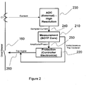
- FIG. 2 shows a block diagram illustrating the working of the invention.
- a specialized circuit, 210 for parallel execution of protection algorithm hence after referred as SOTF core or additional module or second module, is connected to a controller electronics (base module or first module) 220.
- the SOTF core, 210 is interfaced with an ADC that may be either external to both the SOTF core and controller electronics (base module) or may be integral part of the SOTF core.
- ADC, 230 is shown to be external to both.
- the SOTF core performs processing of digitized current signal (sampled current), 240 and also shares information (digitized current signal and processed information), 250 with the controller electronics (base module).
- the architecture has the benefit of off-loading portion of computational burden from controller electronics (base module), 220 to the SOTF core, 210.
- the SOTF core in addition processes digitized analog values to make a trip decision.
- the SOTF core may process at least two full power cycles (50/60 Hz) to make a trip decision.
- the trip signal 260 to the circuit breaker 160 is provided by combining the trip signal from the SOTF core 210 and the trip signal from the controller electronics (base module) 220 by a Boolean "OR" function.
- the SOTF core may process two power cycle data for reliable detection of fault condition.
- the processing by SOTF core may end even before the controller electronics (base module) starts executing the protection algorithm. If the trip command is not served by SOTF core the base module has the power cycle data used by the SOTF core ready for it to further work with protection algorithm, which may be advantageous for fast and efficient processing by the base module.
- FIG. 3 illustrates another embodiment of the invention where a SOTF core 310 consists of ADC and FPGA, 320 is used for measurement and fault detection. Further, there is a provision to electronically isolate the SOTF core with switches 330 once the microcontroller is up and running.
- FPGA 320 is made use for fast parallel execution of measurement and processing algorithms to have significant SOTF time reduction.
- the processing of digitized current signal may be performed to estimate the values of current magnitude along with its harmonics. These values are compared with pre-configured threshold values to determine existence of fault condition.
- the measurement of current signal though in the embodiment is shown for a single phase, is also configurable for measurement of multiple phases.
- the SOTF core may be implemented based on general purpose programmable devices (microcontroller) or custom made programmable devices such as application specific integrated circuit (ASIC) or programmable logic device (PLD).
- microcontroller general purpose programmable devices
- ASIC application specific integrated circuit
- PLD programmable logic device
- the SOTF core may be implemented using analog circuitries or digital or mixed (analog and digital) circuitries without any programmable devices (micro controller, FPGA, ASIC etc) based on electronic (analog/digital) manipulation of current signal to determine signal magnitude including magnitude of harmonics at select frequencies and detect fault condition for trip using comparators.
- the SOTF core electronically is capable to isolate itself, there is no off-loading of any further computational burden after power ON.
- the base module will have to do all its functionalities related to measurement and protection.
- the benefits of electronic isolation may be to reduce power consumption during normal operation as SOTF core need not be powered after the SOTF time duration and the saved power may be used for other functions/ peripherals during the normal functioning of the self-powered relay.
- the SOTF core may be optionally isolated or optionally connected with the base module i.e. at any time, when additional parallel computation may be required for example to process signals with different algorithms to improve confidence on measurement or determination of fault, SOTF core may be optionally connected and initiated accordingly to assist base module with parallel processing.
- the various stages in powering up and execution of tasks for a self-powered relay with a SOTF core is illustrated in Figure 4 .
- the SOTF time contribution with SOTF core is minimized as the SOTF core may begin its processing (digital or analog) on reaching a sufficiently stable voltage, 410.
- the SOTF core being designed as a special circuitry has just the primary task of fault detection with minimal system burden that is completed sooner (420) in comparison with the time for completion of task (430) for fault detection on Power ON by a controller electronics (base module). If any trip decision is arrived at, the trip signal is issued much earlier, at 420 than that with controller electronics (base module), at 430.
- base module controller electronics
- FIG. 5 shows architecture of a self-powered relay with a FPGA SOTF core, 503 along with controller electronics (base module), 505.
- the controller electronics (base module) is depicted as a microcontroller in the figure.
- the SOTF core is interfaced with an ADC, 507 with data and control signal interface 510,
- the FPGA SOTF core also has data and control signal interface, 520 with the microcontroller based controller electronics (base module).
- the FPGA SOTF core performs measurement and processing for faster trip decision.
- the trip signal, 530, from the FPGA SOTF core, referred as instantaneous trip signal is combined using Boolean OR (550) with the trip signal 540 generated from the controller electronics (base module), 505 to have the combined trip signal 560 for a trip coil 570.
- the SOTF performs minimal critical tasks to minimize the SOTF time while the controller performs in addition performs tasks like, Human Machine Interface (HMI) interface, supervision etc.
- HMI Human Machine Interface
- the invention may be realized with use of two or more specialized circuits (additional modules) along with the base module to carry out specialized activity related with any function that a relay may perform, for example functions related to measurement or protection or configuration or diagnostics or HMI.
- the base module or any other circuitry eg power management circuitry in the relay may accordingly initialize the specialized circuits.
- the specialized circuitries may be hosted or organized within a single module (eg within the FPGA SOTF core) or may have additional modules interfaced with base module.
- the self-powered relay may be designed as combinations of specialized circuitry that are organized and managed to improve performance or power management for effective operation of the self-powered relay.
- trip capacitor In a self-power protection device needs to take in account the startup current (i.e. to power on the self-powered device) which needs to be minimum, energy demand for fast charging trip capacitor needs to be controlled such that it is within the available minimum energy budget.
- the trip capacitor need to be isolated from the bus voltage (main voltage) during trip to prevent any rebooting of the protection device during tripping and the circuit design needs to satisfy thermal withstand requirement (20kA for 3 sec, 25kA for 1 sec, 62.5kA for half power cycle).
- FIG 6 shows the sequencing of hardware/software functionalities with respect to the charging of bus capacitor (bus voltage) and trip capacitor and power management scheme is illustrated in Figure 7 .
- the protection relay comprises of power management unit to manage power for various modules including operations related to bus capacitor and trip capacitor.
- the bus voltage (610) is established by charging of bus capacitor (610a) in a controlled manner to the bus voltage through one or more current sensors (710).
- a switch 720 represents control of bus capacitor charging.
- the bus voltage is regulated for various powering needs in the self-powered relay through regulators represented by 730 in Figure 7 .
- the microcontroller and FPGA power up is initiated as soon as sufficient power is available with bus capacitor to maintain the bus voltage through controlled charging.
- the FPGA SOTF core gets ready to process the current and determine fault conditions much before the microcontroller.
- the trip capacitor is also charged through the bus capacitor, controlled through trip capacitor charging and isolation circuit 740 illustrated in Figure 7 through the charging profile 620a to stabilize at 620b to make available energy for trip if fault is detected during the startup of the relay.
- the FPGA SOTF generates a trip signal at the instance illustrated by 630 and the energy from the trip capacitor voltage is made use by discharge 620c.
- the power management is carried out to have SOTF around 40ms by fast charging of trip capacitor without restarting/rebooting of relay or any other effect on performance of the self-power relay.
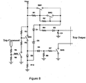
- FIG. 8 provides a scheme to charge the trip capacitor after powering ON the self-powered relay.
- the figure shows all switches SW1 - SW5 with generic switch symbol.
- SW1-SW3 can be realized with PNP transistor
- SW4 can be a NPN transistor
- SW5 can be MOSFET. The functioning of the scheme is explained through mention of the electronic components as referenced in Figure 8 .
- trip capacitor C1 In this scheme, charging of trip capacitor gets started when Vbus exceeds breakdown voltage of D3. Charging current of trip capacitor C1 is limited by current limiting resistor R4 and charging time will be decided by time constant of R4 & C1. In this scheme, capacitor is exponentially charged. During the trip condition, trip capacitor C1 is isolated from Vbus by switches SW1 & SW2.
- trip is command issued by the controller.
- trip capacitor Other means for charging of trip capacitor are possible, for example by adjusting biasing of SW1 & SW2 without series current limiting resistor R4. This will cause an effect of linear charging.
- Another exemplary means for charging of trip capacitor can be by adjusting biasing of SW1 & SW2 as well SW1 current limiting resistor R1. This will cause an effect of linear charging up to certain voltage and then exponential charging of trip capacitor.
Landscapes
- Emergency Protection Circuit Devices (AREA)
Description
- The invention relates to the field of electrical power distribution. The invention specifically relates to protection relay that generates a trip signal to operate a circuit breaker in case of a fault condition.
- A protection relay, also referred as Intelligent Electronic Device (IED), is a microcontroller based intelligent electronic device with a basic function to protect electrical equipment by tripping a circuit breaker and interrupting a power line in case of abnormal situations. The tripping signal for the trip coil or other actuator of the circuit breaker is generated by the protection relay typically when a particular parameter (eg line or phase current) exceeds a nominal or preset value for a predefined time period.
- A self-supplied (self-powered) protection relay utilizes energy from the current sensing transformers to supply to the relay electronics circuit and the energy required to operate trip coils. The design of self-supplied relay has several constraints associated with it to ensure the measurements are accurate and sensitive to avoid any mal-operation. Also, special provisions are required to make its circuitry efficient and optimized for power consumption. Some of these constraints and method to generate power supply by controlled charging for operation of the self-powered relay are disclosed in WIPO publications
WO2009101463 andWO2012056277 . - A self-powered relay requires a minimum time and phase currents to get powered on. Therefore, the measurement and protection functionalities can only be performed after the self-powered relay is powered on from the energy in the circuit involving the electrical equipment being protected. In conditions where the relay is required to switch on in a fault condition i.e. there may be a high current because of the fault, it is desirable that the self-powered relay switches on as fast as possible and also performs detection of fault condition at the earliest to minimize any possibility of damage due to the fault. The delay contributed by switching on of the relay and to detect fault or normal condition to decide on tripping gets reflected as a Switch On To Fault (SOTF) time which is an important parameter to evaluate speed of a protection system.
- Present state of the art protection relay working on microcontrollers with 75 MHZ operating frequency as an example is likely to consume around 50 milliseconds for the activities mainly involving power stabilization (powering up using the line current), power on reset delays (initialization) and non-volatile memory read operations. The controller electronics (base module) starts executing the protection algorithm only after around 50 milliseconds from the instant device is powered on. This duration is a crucial period for SOTF time.
- A protection system with a lower SOTF time is expected to operate faster and is safer. The startup time of the processing device (eg microcontroller) used in a self-powered relays is a major contributing factor to SOTF time. The startup includes time to initialize (boot) and the time to execute the protection algorithm used for the purpose of computing normal/abnormal condition. A reliable and less complex algorithm is certainly preferred to have the SOTF time and reliability within acceptable limits.
- Further, the trip signal from a self-powered relay is provided with help of a trip capacitor that provides the power required to drive the coil. Therefore, in a self-powered relay a fast trip capacitor charging circuit to have faster SOTF is required and the charging method needs to be developed considering challenges in a self-power device.
-
US 2003/063422 A1 discloses a circuit breaker having a trip mechanism and an electronic module having an application specific integrated circuit (ASIC), a control circuit, a composite which generates a composite signal voltage, a residual circuit, the circuit breaker comprising a first power supply to provide a first voltage signal and a second power supply to provide a second voltage signal. An analog override circuit in the circuit breaker is configured to receive the first voltage signal from the first power supply, the second voltage signal from the second power supply and the composite signal voltage from the composite circuit. The analog override circuit provides an override signal to the ASIC which is coupled to a logic gate configured to receive a first trip signal from the control circuit and a second trip signal from the ASIC and provides a third trip signal to the trip mechanism. -
US 4 347 541 A discloses an instantaneous trip circuit, a ground fault detector. and both short term and long term delay circuits providing trip signals upon certain conditions. Upon the presence of any trip signal, an OR circuit provides a control signal to gate an SCR having a thermal switch coupled across its anode and cathode. A supply voltage is applied across a serial connection to the anode, the cathode. and the solenoid. -
EP 1 589 629 A2 describes an electronic self-supplied protection device for automatic circuit-breakers comprising: a supply device that draws energy from the stretch of electrical network protected by said circuit-breaker; a control device comprising at least two levels of operation, the first of said at least two levels of operation being associated to the function of protection from instantaneous short-circuit, the second and possible further levels of operation being associated to further functions of said protection device; a selective interface device comprising means for regulating the supply, which, in a first step, immediately following upon closing of the circuit by the circuit-breaker, supply said first level of operation, and, after a controlled period of time, supply also said second and possible further levels of operation of said control device. - Thus, in a self-powered relay, minimizing the SOTF time requires further consideration and this is an important object of the invention.
- The object of the invention is to minimize the time to Switch On to Fault (SOTF). In one aspect of the invention, a protection relay is provided. The protection relay has a base module, also referred as a first module comprising of all the functionality required for operation of the relay and additional one or more specialized modules, being referred as additional modules, to boost performance. For SOTF enhancement in a self-powered protection relay, i.e. to reduce the time for SOTF specially in a self-powered protection relay, the additional module (referred as SOTF core or second module) comprises power and time efficient circuitries to execute measurement and protection related tasks efficiently.
- The invention is performed according to the object of appended independent claim 1.
- In one embodiment, the trip signal for the circuit breaker is generated based on the trip signal from the first module and the trip signal from the additional module. The trip signal from the first module and the trip signal from the additional module in an embodiment may be logically combined with an "OR" logic to produce the trip signal from the protection relay for the circuit breaker. From the view of reducing SOTF, the trip signal from the additional module is produced with efficient processing using as an example, Field Programmable Gate Array (FPGA) modules to have power and time efficient means to carry out processing. The additional module (second module) performs tasks related to decision for generating trip signal much faster than that by the first module. The decision for generating trip signal is made on the basis of comparing the magnitude of measured current and magnitude of harmonics content in at least one specific frequency with a preconfigured values in the relay based on its settings. The trip signal can result also from other algorithms used for determining the conditions for trip.
- In yet another embodiment, the additional module can be comprising of a programmable device such as a microcontroller or a microprocessor based circuits or application specific integrated circuit (ASIC) or programmable logic device (PLD).
- In yet another embodiment, the additional module can comprise of analog circuits comprising of analog filters and comparators.
- In yet another embodiment, the additional module can comprise of digital circuits.
- In yet another embodiment, the additional module configured for having faster SOTF value is used only during the Power ON of the protection relay. The additional module may be electronically isolated after the first module is fully functional and operative after the Power ON of the protection relay.
- In yet another embodiment, one or more additional modules are used along with the first module and the one or more additional modules are programmatically isolated or connected to work together with the first module to carry out any function related to measurement and analysis of power parameters (current, voltage, frequency etc) or to carry out functions related to configuration, diagnostics or human machine interface (HMI) functions.
- In another aspect of the invention, a protection relay comprises a power management unit that is configured to provide power to various modules of the protection relay including a first module and a second module by controlled charging of a bus capacitor from the current which the protection relay is measuring. The power management unit also performs electronic isolation of the bus capacitor during measurement of the current so that the measurements are accurate.
- In another embodiment, the protection relay comprises a power management unit that performs controlled charging of a trip capacitor from the bus capacitor. Also the controlled charging of the trip capacitor includes electronic isolation of the trip capacitor from the bus capacitor during the trip signal generation to operate the circuit breaker connected in the line.
- In yet another embodiment, the controlled charging of the trip capacitor is made such that sufficient energy is available by fast charging to operate the circuit breaker before the generation of the trip signal to operate the circuit breaker. Thus ensuring that SOTF time is minimized not just by having efficient computation means but also minimized time for charging trip capacitor responsible for providing energy during trip operation.
- Other features and advantages will become apparent to those skilled in the art upon reading the description of the preferred exemplary embodiments in conjunction with the accompanying drawings, wherein:
-
Figure 1 is a block diagram of a protection system having a protection relay; -
Figure 2 is a block diagram of a protection system having a protection relay with SOTF core; -
Figure 3 is a block diagram of a protection system having a protection relay with FPGA based SOTF core; -
Figure 4 illustrates various stages in powering up and execution of tasks for a self-powered relay with a SOTF core; -
Figure 5 is a block diagram of a self-powered relay with a FPGA SOTF core; -
Figure 6 illustrates controlled charging of bus capacitor and trip capacitor sequenced with operation of a self-powered relay; -
Figure 7 illustrates power extraction and management in a self-powered relay; and -
Figure 8 is an exemplary scheme to charge and discharge trip capacitor in a self-powered relay. -
Figure 1 shows a basic block diagram of a protection system with a protection relay connected for protection. The self-powered relay has measurement and protection algorithms executed using acontroller electronics 110. Thecontroller electronics 110, also referred as base module senses the current using a current sensor (current transformer) 120, samples and digitizes thecurrent signal 125 using analog to digital convertor (ADC) 130 and performs computation on the sampled digital data with a measurement andprotection component 140 to decide whether or not to serve thetrip command 150 forcircuit breaker 160. Thecurrent signal 125 is also used to generate power for the relay (not shown inFigure 1 ) in case of a self-powered protection relay. Further, the figure is described using current as an example of the electrical parameter being measured but it can be noted that a relay (IED) can be used for measurement or/and protection purpose involving measurement and analysis of multiple electrical parameters (current, voltage, frequency etc). - The SOTF time contribution by the base module in a self-powered relay may be visualized with respect to self-powering activity within the self-powered relay to reach a stable power for itself. The voltage build up happens with the measured current signal and on reaching a specific voltage level (trigger voltage level) from the powering ON the relay, the power management and system critical tasks are performed including initialization of electronics in the self-powered relay. As the voltage further builds up and reaches power-up stage where sufficiently stable voltage is available for the system devices, a power on reset signal is provided to the base module. Subsequently the base module gets initialized and performs read cycles involving external nonvolatile memory. On successful initialization the base module executes the tasks to detect the fault and serve trip command at SOTF time.
- SOTF time may be minimized if there is an efficient way to have the computing device to initialize (boot) and execute the protection algorithm used for the purpose of computing normal/abnormal condition immediately at the power-up stage. This is realized for a self-powered relay by providing a parallel specialized circuit for fast booting and efficient execution of protection algorithm to minimize the SOTF time. The specialized circuit being parallel needs to be efficient also for power consumption. Further, the parallel specialized circuit may be designed to be specialized only to execute critical task, here, in this case SOTF task and would not have the burden of any general purpose or system activities that the base module used in self-powered relay is required to carry out.
-
Figure 2 shows a block diagram illustrating the working of the invention. A specialized circuit, 210 for parallel execution of protection algorithm, hence after referred as SOTF core or additional module or second module, is connected to a controller electronics (base module or first module) 220. The SOTF core, 210 is interfaced with an ADC that may be either external to both the SOTF core and controller electronics (base module) or may be integral part of the SOTF core. In the embodiment, shown inFigure 2 , ADC, 230 is shown to be external to both. The SOTF core performs processing of digitized current signal (sampled current), 240 and also shares information (digitized current signal and processed information), 250 with the controller electronics (base module). The architecture has the benefit of off-loading portion of computational burden from controller electronics (base module), 220 to the SOTF core, 210. The SOTF core in addition processes digitized analog values to make a trip decision. The SOTF core may process at least two full power cycles (50/60 Hz) to make a trip decision. Thetrip signal 260 to thecircuit breaker 160 is provided by combining the trip signal from theSOTF core 210 and the trip signal from the controller electronics (base module) 220 by a Boolean "OR" function. The SOTF core may process two power cycle data for reliable detection of fault condition. - As SOTF core is a specialized circuit, the processing by SOTF core may end even before the controller electronics (base module) starts executing the protection algorithm. If the trip command is not served by SOTF core the base module has the power cycle data used by the SOTF core ready for it to further work with protection algorithm, which may be advantageous for fast and efficient processing by the base module.
-
Figure 3 illustrates another embodiment of the invention where aSOTF core 310 consists of ADC and FPGA, 320 is used for measurement and fault detection. Further, there is a provision to electronically isolate the SOTF core withswitches 330 once the microcontroller is up and running. In this embodiment,FPGA 320 is made use for fast parallel execution of measurement and processing algorithms to have significant SOTF time reduction. The processing of digitized current signal may be performed to estimate the values of current magnitude along with its harmonics. These values are compared with pre-configured threshold values to determine existence of fault condition. The measurement of current signal, though in the embodiment is shown for a single phase, is also configurable for measurement of multiple phases. - In other embodiments, the SOTF core (additional module) may be implemented based on general purpose programmable devices (microcontroller) or custom made programmable devices such as application specific integrated circuit (ASIC) or programmable logic device (PLD).
- In another embodiment, the SOTF core may be implemented using analog circuitries or digital or mixed (analog and digital) circuitries without any programmable devices (micro controller, FPGA, ASIC etc) based on electronic (analog/digital) manipulation of current signal to determine signal magnitude including magnitude of harmonics at select frequencies and detect fault condition for trip using comparators.
- In the embodiment illustrated in
Figure 3 , as the SOTF core electronically is capable to isolate itself, there is no off-loading of any further computational burden after power ON. The base module will have to do all its functionalities related to measurement and protection. The benefits of electronic isolation may be to reduce power consumption during normal operation as SOTF core need not be powered after the SOTF time duration and the saved power may be used for other functions/ peripherals during the normal functioning of the self-powered relay. - In another embodiment, the SOTF core may be optionally isolated or optionally connected with the base module i.e. at any time, when additional parallel computation may be required for example to process signals with different algorithms to improve confidence on measurement or determination of fault, SOTF core may be optionally connected and initiated accordingly to assist base module with parallel processing.
- The various stages in powering up and execution of tasks for a self-powered relay with a SOTF core is illustrated in
Figure 4 . The SOTF time contribution with SOTF core is minimized as the SOTF core may begin its processing (digital or analog) on reaching a sufficiently stable voltage, 410. The SOTF core being designed as a special circuitry has just the primary task of fault detection with minimal system burden that is completed sooner (420) in comparison with the time for completion of task (430) for fault detection on Power ON by a controller electronics (base module). If any trip decision is arrived at, the trip signal is issued much earlier, at 420 than that with controller electronics (base module), at 430. Thus the provision with SOTF core provides significant SOTF time reduction. -
Figure 5 shows architecture of a self-powered relay with a FPGA SOTF core, 503 along with controller electronics (base module), 505. The controller electronics (base module) is depicted as a microcontroller in the figure. The SOTF core is interfaced with an ADC, 507 with data andcontrol signal interface 510, The FPGA SOTF core also has data and control signal interface, 520 with the microcontroller based controller electronics (base module). The FPGA SOTF core performs measurement and processing for faster trip decision. The trip signal, 530, from the FPGA SOTF core, referred as instantaneous trip signal is combined using Boolean OR (550) with thetrip signal 540 generated from the controller electronics (base module), 505 to have the combinedtrip signal 560 for atrip coil 570. The SOTF performs minimal critical tasks to minimize the SOTF time while the controller performs in addition performs tasks like, Human Machine Interface (HMI) interface, supervision etc. - As another embodiment, the invention may be realized with use of two or more specialized circuits (additional modules) along with the base module to carry out specialized activity related with any function that a relay may perform, for example functions related to measurement or protection or configuration or diagnostics or HMI. The base module or any other circuitry eg power management circuitry in the relay may accordingly initialize the specialized circuits. The specialized circuitries may be hosted or organized within a single module (eg within the FPGA SOTF core) or may have additional modules interfaced with base module. It may be noted that the self-powered relay may be designed as combinations of specialized circuitry that are organized and managed to improve performance or power management for effective operation of the self-powered relay.
- To achieve successful and fast tripping during minimum SOTF condition, sufficient energy should be available as soon as possible once current starts flows through the sensing current transformer (CT). This energy is stored in a capacitor, known as trip capacitor. Fast charging of trip capacitor should not affect functioning of other circuit of the protection relay as the protection relay is fully self-powered from the current such that powering does not affect the working of microcontroller, accuracy of current measurement or detection of fault conditions. Therefore the charging needs to be controlled for the rate of charging and also the manner this charging is scheduled with respect to powering or measurement/analysis function carried out by the relay. Thus, in a self-powered relay, hardware design is optimized for startup time for performance and power consumption which requires tight coupling between the hardware/software functionalities with power management scheme.
- To achieve fast charging of trip capacitor in a self-power protection device needs to take in account the startup current (i.e. to power on the self-powered device) which needs to be minimum, energy demand for fast charging trip capacitor needs to be controlled such that it is within the available minimum energy budget. The trip capacitor need to be isolated from the bus voltage (main voltage) during trip to prevent any rebooting of the protection device during tripping and the circuit design needs to satisfy thermal withstand requirement (20kA for 3 sec, 25kA for 1 sec, 62.5kA for half power cycle).
-
Figure 6 shows the sequencing of hardware/software functionalities with respect to the charging of bus capacitor (bus voltage) and trip capacitor and power management scheme is illustrated inFigure 7 . The protection relay comprises of power management unit to manage power for various modules including operations related to bus capacitor and trip capacitor. In the figure, the bus voltage (610) is established by charging of bus capacitor (610a) in a controlled manner to the bus voltage through one or more current sensors (710). InFigure 7 , aswitch 720 represents control of bus capacitor charging. The bus voltage is regulated for various powering needs in the self-powered relay through regulators represented by 730 inFigure 7 . The microcontroller and FPGA power up is initiated as soon as sufficient power is available with bus capacitor to maintain the bus voltage through controlled charging. As discussed earlier, the FPGA SOTF core gets ready to process the current and determine fault conditions much before the microcontroller. The trip capacitor is also charged through the bus capacitor, controlled through trip capacitor charging andisolation circuit 740 illustrated inFigure 7 through the chargingprofile 620a to stabilize at 620b to make available energy for trip if fault is detected during the startup of the relay. In an event of the fault the FPGA SOTF generates a trip signal at the instance illustrated by 630 and the energy from the trip capacitor voltage is made use bydischarge 620c. The power management is carried out to have SOTF around 40ms by fast charging of trip capacitor without restarting/rebooting of relay or any other effect on performance of the self-power relay. -
Figure 8 provides a scheme to charge the trip capacitor after powering ON the self-powered relay. The figure shows all switches SW1 - SW5 with generic switch symbol. In an exemplary embodiment, SW1-SW3 can be realized with PNP transistor, SW4 can be a NPN transistor and SW5 can be MOSFET. The functioning of the scheme is explained through mention of the electronic components as referenced inFigure 8 . - In this scheme, charging of trip capacitor gets started when Vbus exceeds breakdown voltage of D3. Charging current of trip capacitor C1 is limited by current limiting resistor R4 and charging time will be decided by time constant of R4 & C1. In this scheme, capacitor is exponentially charged. During the trip condition, trip capacitor C1 is isolated from Vbus by switches SW1 & SW2.
- When the relay is energized with CT input, the energy is stored in bus capacitor (Vbus) to supply power to the relay.
- Charging of trip capacitor starts as Vbus exceeds breakdown voltage of zener diode D3. Now, biasing current of SW2 start flowing through path Vbus → R1 → R2 → D1 → D3 → R10 → Ground. So, SW2 is turned ON.
- Once SW2 is turned ON, SW1 will get the biasing current (which is DC gain of SW2 times biasing current of SW2) and it will turned on and start charging of trip capacitor C1 through Vbus → SW1 → R4 → D2 → C1 → Ground. Series resistor is R4 is kept to limit the charging current. Diode D2 is kept in series path to avoid discharging of trip capacitor through the charging circuit.
- As relay detects the fault, trip is command issued by the controller.
- Trip command will turn on SW4. As SW4 is turned on, switch SW3 will get biasing through path Vbus → R3 → R5 → SW4 → Ground and it will be turned on.
- Once SW3 is turned on zener diode D3 will be forward biased through path Vbus → SW3 → D5 → D3. Now, SW2 will not get biasing current and stops conducting which in turn will stop biasing of SW1. Hence, SW1 is turned off and trip capacitor is disconnected from the Vbus.
- At the same instant, SW5 will get biasing through Vbus → SW3 → D4 (zener diode) → R9 → Ground. And trip capacitor is discharged through path C1 → Trip output → SW5 → Ground.
- Other means for charging of trip capacitor are possible, for example by adjusting biasing of SW1 & SW2 without series current limiting resistor R4. This will cause an effect of linear charging. Another exemplary means for charging of trip capacitor can be by adjusting biasing of SW1 & SW2 as well SW1 current limiting resistor R1. This will cause an effect of linear charging up to certain voltage and then exponential charging of trip capacitor.
- Thus, fast charging of trip capacitor within power budget is achieved to support trip operation on detection of fault during initialization of the base module of the self-powered relay.
- While only certain features of the invention have been illustrated and described herein, many modifications and changes will occur to those skilled in the art. Various illustrations in the invention is made with specific exemplary conditions related to a self-powered relay and these conditions may equally be applicable for a protection relay that has a dedicated power source. Further, examples for over current protection with measurement of current are also applicable for over voltage protection with measurement of line voltage or for other power parameters for which a relay or an IED may be used. It is, therefore, to be understood that the appended claims are intended to cover all such modifications and changes as fall within the scope of the appended claims.
Claims (13)
- A protection relay configured to measure current in a power line with at least one current sensor connected in the power line, and to analyze the measured current for providing electrical protection by generating a trip signal (560) to operate a circuit breaker connected in the power line, the protection relay comprising:a first module (505) for analyzing the measured current in the power line and for providing electrical protection by generating a first trip signal (540) based on the analyzed measured current by the first module;a second module (503) for analyzing the measured current in the power line and for providing electrical protection by generating a second trip signal (530) based on the analyzed measured current by the second module;wherein, the trip signal (560) to operate the circuit breaker connected in the power line is generated by logical combination of the first trip signal (540) from the first module (505) and the second trip signal (530) from the second module (503), andwherein the protection relay comprises a power management unit that performs controlled charging of a trip capacitor (760) from a bus capacitor (750).
- The protection relay as described in Claim 1, wherein the power management unit is configured to provide power to the first module and the second module by controlled charging of the bus capacitor (750) from the current.
- The protection relay as described in Claim 2, wherein the controlled charging of the bus capacitor includes isolating the bus capacitor from the controlled charging of the bus capacitor during measurement of current using the at least one current sensor.
- The protection relay as described in Claim 1, wherein the controlled charging of the trip capacitor includes isolating the trip capacitor from the bus capacitor during operation of the circuit breaker.
- The protection relay as described in Claim 1, wherein the controlled charging of the trip capacitor, to an energy capacity sufficiently capable to operate the circuit breaker is completed before generation of the trip signal (560) to operate the circuit breaker.
- The protection relay as described in Claim 1, wherein the said second module for analyzing the measured current includes analysis based on comparing magnitude of the measured current and magnitude of at least one harmonic frequency in the measured current with a pre-configured value.
- The protection relay as described in Claim 1, wherein the said second module for analyzing the measured current is realized with a Field Programmable Gate Array (FPGA) module.
- The protection relay as described in Claim 1, wherein the said second module for analyzing the measured current is realized with a programmable devices including microcontroller or microprocessor based circuitry.
- The protection relay as described in Claim 1, wherein the said second module for analyzing the measured current is realized with an analog circuitry comprising of analog filters and analog comparators.
- The protection relay as described in Claim 1, the analyses of the measured current in the power line, for providing electrical protection by generation of the second trip signal, by the said second module is performed faster than the analyses of the measured current in the power line, for providing electrical protection by generation of the first trip signal, by the said first module.
- The protection relay as described in Claim 1, wherein the said second module for analyzing the measured current in the power line and for providing electrical protection by generation of the second trip signal is used during the Power ON of the protection relay.
- The protection relay as described in Claim 1, wherein the said second module for analyzing the measured current in the power line and for providing electrical protection by generation of the second trip signal is used only during the Power ON of the protection relay and is electronically isolated after the first module is functionally fully operative after the Power ON of the protection relay.
- The protection relay as described in Claim 1, wherein the second module is programmatically isolated or connected to work together with the first module to measure or analyze power parameters in the power line or perform configuration, diagnostics or human machine interface (HMI) functions.
Applications Claiming Priority (3)
| Application Number | Priority Date | Filing Date | Title |
|---|---|---|---|
| IN5044CH2012 | 2012-12-04 | ||
| IN1464CH2013 | 2013-04-01 | ||
| PCT/IB2013/001791 WO2014087205A1 (en) | 2012-12-04 | 2013-08-19 | A self supplied protection relay with a module to boost performance |
Publications (2)
| Publication Number | Publication Date |
|---|---|
| EP2929606A1 EP2929606A1 (en) | 2015-10-14 |
| EP2929606B1 true EP2929606B1 (en) | 2017-12-20 |
Family
ID=54142990
Family Applications (1)
| Application Number | Title | Priority Date | Filing Date |
|---|---|---|---|
| EP13783373.7A Active EP2929606B1 (en) | 2012-12-04 | 2013-08-19 | A self supplied protection relay with a module to boost performance |
Country Status (4)
| Country | Link |
|---|---|
| US (1) | US9887530B2 (en) |
| EP (1) | EP2929606B1 (en) |
| CN (1) | CN105144526B (en) |
| WO (1) | WO2014087205A1 (en) |
Cited By (1)
| Publication number | Priority date | Publication date | Assignee | Title |
|---|---|---|---|---|
| EP4697530A1 (en) * | 2024-07-16 | 2026-02-18 | Citel | Protection apparatus for protecting a surge protection device |
Families Citing this family (6)
| Publication number | Priority date | Publication date | Assignee | Title |
|---|---|---|---|---|
| US11088530B2 (en) * | 2017-04-18 | 2021-08-10 | The Government Of The United States Of America, As Represented By The Secretary Of The Navy | Highly variable and adjustable current circuit breaker |
| CN107658838B (en) * | 2017-11-06 | 2023-12-26 | 湖南电铨科技股份有限公司 | AC single-phase intelligent module |
| US10922203B1 (en) * | 2018-09-21 | 2021-02-16 | Nvidia Corporation | Fault injection architecture for resilient GPU computing |
| FR3114681B1 (en) * | 2020-09-30 | 2023-02-10 | Schneider Electric Ind Sas | Electrical protection device |
| US11862958B2 (en) * | 2021-10-04 | 2024-01-02 | Schweitzer Engineering Laboratories, Inc. | Isolation of protection functions in electrical power systems during startup |
| CN115986904A (en) * | 2022-12-08 | 2023-04-18 | 亨斯迈(杭州)电力技术有限公司 | A protection measurement and control system for standby automatic switching |
Family Cites Families (14)
| Publication number | Priority date | Publication date | Assignee | Title |
|---|---|---|---|---|
| FR2479556A1 (en) * | 1980-03-31 | 1981-10-02 | Merlin Gerin | IMPROVED STATIC SENSOR FOR ELECTRICAL CIRCUIT BREAKER |
| US4347541A (en) * | 1981-01-14 | 1982-08-31 | Gte Laboratories Incorporated | Circuit breaker |
| US4442472A (en) * | 1982-03-26 | 1984-04-10 | Siemens-Allis, Inc. | Solid state trip circuit with digital timer |
| US6496342B1 (en) | 1999-02-12 | 2002-12-17 | Bitronics Inc. | Distributed monitoring and protection system for a distributed power network |
| US6621672B2 (en) * | 2001-10-01 | 2003-09-16 | Siemens Energy & Automation, Inc. | Circuit breaker having analog override |
| ITMI20040759A1 (en) | 2004-04-19 | 2004-07-19 | Abb Service Srl | SELF-POWERED ELECTRONIC PROTECTION DEVICE FOR AUTOMATIC SWITCHES |
| EP2255424B1 (en) | 2008-02-15 | 2018-08-22 | ABB Schweiz AG | A standalone self-supplied numeric controlled relay |
| JP5056478B2 (en) * | 2008-02-28 | 2012-10-24 | 富士通株式会社 | Leak current analysis program, recording medium recording the program, leak current analysis apparatus, and leak current analysis method |
| CN201838536U (en) * | 2010-08-23 | 2011-05-18 | 北京恒源华清电力科技有限公司 | Self-power supply type digital relay |
| WO2012056277A1 (en) | 2010-10-28 | 2012-05-03 | Abb Technology Ltd | Human-machine interface for a self-supplied relay |
| BR112013010580A8 (en) | 2010-10-28 | 2017-12-19 | Abb Schweiz Ag | PROTECTION RELAY FOR SENSITIVE EARTH FAULT PROTECTION |
| US8665574B2 (en) * | 2010-11-12 | 2014-03-04 | Schneider Electric USA, Inc. | Thermal memory in a fault powered system |
| CN101980419B (en) * | 2010-12-09 | 2012-07-18 | 天津市海川电力技术有限公司 | Automatic control device for vacuum circuit breaker on electric distribution network |
| US8649146B2 (en) | 2010-12-17 | 2014-02-11 | General Electric Company | Capacitance check and current monitoring circuit for use with a circuit protection device |
-
2013
- 2013-08-19 CN CN201380072241.0A patent/CN105144526B/en active Active
- 2013-08-19 WO PCT/IB2013/001791 patent/WO2014087205A1/en not_active Ceased
- 2013-08-19 EP EP13783373.7A patent/EP2929606B1/en active Active
-
2015
- 2015-06-04 US US14/730,785 patent/US9887530B2/en active Active
Cited By (1)
| Publication number | Priority date | Publication date | Assignee | Title |
|---|---|---|---|---|
| EP4697530A1 (en) * | 2024-07-16 | 2026-02-18 | Citel | Protection apparatus for protecting a surge protection device |
Also Published As
| Publication number | Publication date |
|---|---|
| CN105144526B (en) | 2018-03-30 |
| EP2929606A1 (en) | 2015-10-14 |
| WO2014087205A1 (en) | 2014-06-12 |
| US9887530B2 (en) | 2018-02-06 |
| US20150270697A1 (en) | 2015-09-24 |
| CN105144526A (en) | 2015-12-09 |
Similar Documents
| Publication | Publication Date | Title |
|---|---|---|
| US9887530B2 (en) | Self supplied protection relay with a module to boost performance | |
| US7869170B2 (en) | Method and system for time synchronized trip algorithms for breaker self protection | |
| US7683586B2 (en) | Method and system of fault powered supply voltage regulation | |
| CN113454866A (en) | Method and apparatus for controlling power supply to protected electrical loads | |
| EP2188824B1 (en) | Method and apparatus for executing secondary functions on an electrical switchgear device | |
| EP1048103B1 (en) | Method for performing instantaneous protection in a trip unit | |
| EP0995251B1 (en) | Solid state overload relay | |
| EP2254214B1 (en) | Circuit breaker and method of controlling its operation | |
| JP6105643B2 (en) | Earth leakage breaker | |
| US7791849B2 (en) | Redundant trip activation | |
| US20200099218A1 (en) | Intelligent three-phase power switch controller | |
| CN100546141C (en) | Self-Powered Electronic Protection Devices for Automatic Circuit Breakers | |
| KR101312103B1 (en) | Digital protection relay | |
| EP2408078A2 (en) | Centrally controlled protection system having reduced energy let-through mode | |
| US20070076335A1 (en) | Protection apparatus for an electrical load | |
| WO2015075614A1 (en) | Power management in a self-supplied protection relay | |
| JP4998119B2 (en) | Circuit breaker | |
| US20250105616A1 (en) | Switching device and method for protecting an electrical load against overcurrent | |
| JP2007028858A (en) | Pack battery | |
| KR100781889B1 (en) | Malfunction prevention device and prevention method of ground overcurrent relay | |
| CN112993932A (en) | Digital control delay cycle-by-cycle current-limiting protection method and device | |
| EP4128459A1 (en) | A motor-protective circuit breaker comprising an automatic setup function and a method of using such a circuit breaker | |
| CN114336520B (en) | Electrical protection unit | |
| CN103683180A (en) | Methods, systems, and apparatus for automated maintenance mode switching | |
| KR20150029169A (en) | Over current relay based on the low power mode of the cpu |
Legal Events
| Date | Code | Title | Description |
|---|---|---|---|
| PUAI | Public reference made under article 153(3) epc to a published international application that has entered the european phase |
Free format text: ORIGINAL CODE: 0009012 |
|
| 17P | Request for examination filed |
Effective date: 20150624 |
|
| AK | Designated contracting states |
Kind code of ref document: A1 Designated state(s): AL AT BE BG CH CY CZ DE DK EE ES FI FR GB GR HR HU IE IS IT LI LT LU LV MC MK MT NL NO PL PT RO RS SE SI SK SM TR |
|
| AX | Request for extension of the european patent |
Extension state: BA ME |
|
| DAX | Request for extension of the european patent (deleted) | ||
| GRAP | Despatch of communication of intention to grant a patent |
Free format text: ORIGINAL CODE: EPIDOSNIGR1 |
|
| RIC1 | Information provided on ipc code assigned before grant |
Ipc: H02H 3/05 20060101ALI20170619BHEP Ipc: H02H 3/093 20060101ALI20170619BHEP Ipc: H02H 1/06 20060101AFI20170619BHEP Ipc: H02H 3/52 20060101ALI20170619BHEP Ipc: H02H 3/16 20060101ALI20170619BHEP Ipc: H02H 3/10 20060101ALI20170619BHEP |
|
| INTG | Intention to grant announced |
Effective date: 20170706 |
|
| GRAS | Grant fee paid |
Free format text: ORIGINAL CODE: EPIDOSNIGR3 |
|
| GRAA | (expected) grant |
Free format text: ORIGINAL CODE: 0009210 |
|
| AK | Designated contracting states |
Kind code of ref document: B1 Designated state(s): AL AT BE BG CH CY CZ DE DK EE ES FI FR GB GR HR HU IE IS IT LI LT LU LV MC MK MT NL NO PL PT RO RS SE SI SK SM TR |
|
| REG | Reference to a national code |
Ref country code: GB Ref legal event code: FG4D |
|
| REG | Reference to a national code |
Ref country code: CH Ref legal event code: EP |
|
| REG | Reference to a national code |
Ref country code: IE Ref legal event code: FG4D |
|
| REG | Reference to a national code |
Ref country code: AT Ref legal event code: REF Ref document number: 957192 Country of ref document: AT Kind code of ref document: T Effective date: 20180115 |
|
| REG | Reference to a national code |
Ref country code: DE Ref legal event code: R096 Ref document number: 602013031112 Country of ref document: DE |
|
| REG | Reference to a national code |
Ref country code: NL Ref legal event code: MP Effective date: 20171220 |
|
| PG25 | Lapsed in a contracting state [announced via postgrant information from national office to epo] |
Ref country code: SE Free format text: LAPSE BECAUSE OF FAILURE TO SUBMIT A TRANSLATION OF THE DESCRIPTION OR TO PAY THE FEE WITHIN THE PRESCRIBED TIME-LIMIT Effective date: 20171220 Ref country code: LT Free format text: LAPSE BECAUSE OF FAILURE TO SUBMIT A TRANSLATION OF THE DESCRIPTION OR TO PAY THE FEE WITHIN THE PRESCRIBED TIME-LIMIT Effective date: 20171220 Ref country code: NO Free format text: LAPSE BECAUSE OF FAILURE TO SUBMIT A TRANSLATION OF THE DESCRIPTION OR TO PAY THE FEE WITHIN THE PRESCRIBED TIME-LIMIT Effective date: 20180320 Ref country code: FI Free format text: LAPSE BECAUSE OF FAILURE TO SUBMIT A TRANSLATION OF THE DESCRIPTION OR TO PAY THE FEE WITHIN THE PRESCRIBED TIME-LIMIT Effective date: 20171220 |
|
| REG | Reference to a national code |
Ref country code: LT Ref legal event code: MG4D |
|
| REG | Reference to a national code |
Ref country code: AT Ref legal event code: MK05 Ref document number: 957192 Country of ref document: AT Kind code of ref document: T Effective date: 20171220 |
|
| PG25 | Lapsed in a contracting state [announced via postgrant information from national office to epo] |
Ref country code: HR Free format text: LAPSE BECAUSE OF FAILURE TO SUBMIT A TRANSLATION OF THE DESCRIPTION OR TO PAY THE FEE WITHIN THE PRESCRIBED TIME-LIMIT Effective date: 20171220 Ref country code: LV Free format text: LAPSE BECAUSE OF FAILURE TO SUBMIT A TRANSLATION OF THE DESCRIPTION OR TO PAY THE FEE WITHIN THE PRESCRIBED TIME-LIMIT Effective date: 20171220 Ref country code: GR Free format text: LAPSE BECAUSE OF FAILURE TO SUBMIT A TRANSLATION OF THE DESCRIPTION OR TO PAY THE FEE WITHIN THE PRESCRIBED TIME-LIMIT Effective date: 20180321 Ref country code: BG Free format text: LAPSE BECAUSE OF FAILURE TO SUBMIT A TRANSLATION OF THE DESCRIPTION OR TO PAY THE FEE WITHIN THE PRESCRIBED TIME-LIMIT Effective date: 20180320 Ref country code: RS Free format text: LAPSE BECAUSE OF FAILURE TO SUBMIT A TRANSLATION OF THE DESCRIPTION OR TO PAY THE FEE WITHIN THE PRESCRIBED TIME-LIMIT Effective date: 20171220 |
|
| PG25 | Lapsed in a contracting state [announced via postgrant information from national office to epo] |
Ref country code: NL Free format text: LAPSE BECAUSE OF FAILURE TO SUBMIT A TRANSLATION OF THE DESCRIPTION OR TO PAY THE FEE WITHIN THE PRESCRIBED TIME-LIMIT Effective date: 20171220 |
|
| PG25 | Lapsed in a contracting state [announced via postgrant information from national office to epo] |
Ref country code: EE Free format text: LAPSE BECAUSE OF FAILURE TO SUBMIT A TRANSLATION OF THE DESCRIPTION OR TO PAY THE FEE WITHIN THE PRESCRIBED TIME-LIMIT Effective date: 20171220 Ref country code: CZ Free format text: LAPSE BECAUSE OF FAILURE TO SUBMIT A TRANSLATION OF THE DESCRIPTION OR TO PAY THE FEE WITHIN THE PRESCRIBED TIME-LIMIT Effective date: 20171220 Ref country code: CY Free format text: LAPSE BECAUSE OF FAILURE TO SUBMIT A TRANSLATION OF THE DESCRIPTION OR TO PAY THE FEE WITHIN THE PRESCRIBED TIME-LIMIT Effective date: 20171220 Ref country code: ES Free format text: LAPSE BECAUSE OF FAILURE TO SUBMIT A TRANSLATION OF THE DESCRIPTION OR TO PAY THE FEE WITHIN THE PRESCRIBED TIME-LIMIT Effective date: 20171220 Ref country code: SK Free format text: LAPSE BECAUSE OF FAILURE TO SUBMIT A TRANSLATION OF THE DESCRIPTION OR TO PAY THE FEE WITHIN THE PRESCRIBED TIME-LIMIT Effective date: 20171220 |
|
| REG | Reference to a national code |
Ref country code: FR Ref legal event code: PLFP Year of fee payment: 6 |
|
| PG25 | Lapsed in a contracting state [announced via postgrant information from national office to epo] |
Ref country code: PL Free format text: LAPSE BECAUSE OF FAILURE TO SUBMIT A TRANSLATION OF THE DESCRIPTION OR TO PAY THE FEE WITHIN THE PRESCRIBED TIME-LIMIT Effective date: 20171220 Ref country code: SM Free format text: LAPSE BECAUSE OF FAILURE TO SUBMIT A TRANSLATION OF THE DESCRIPTION OR TO PAY THE FEE WITHIN THE PRESCRIBED TIME-LIMIT Effective date: 20171220 Ref country code: IS Free format text: LAPSE BECAUSE OF FAILURE TO SUBMIT A TRANSLATION OF THE DESCRIPTION OR TO PAY THE FEE WITHIN THE PRESCRIBED TIME-LIMIT Effective date: 20180420 Ref country code: RO Free format text: LAPSE BECAUSE OF FAILURE TO SUBMIT A TRANSLATION OF THE DESCRIPTION OR TO PAY THE FEE WITHIN THE PRESCRIBED TIME-LIMIT Effective date: 20171220 Ref country code: IT Free format text: LAPSE BECAUSE OF FAILURE TO SUBMIT A TRANSLATION OF THE DESCRIPTION OR TO PAY THE FEE WITHIN THE PRESCRIBED TIME-LIMIT Effective date: 20171220 Ref country code: AT Free format text: LAPSE BECAUSE OF FAILURE TO SUBMIT A TRANSLATION OF THE DESCRIPTION OR TO PAY THE FEE WITHIN THE PRESCRIBED TIME-LIMIT Effective date: 20171220 |
|
| REG | Reference to a national code |
Ref country code: DE Ref legal event code: R097 Ref document number: 602013031112 Country of ref document: DE |
|
| PLBE | No opposition filed within time limit |
Free format text: ORIGINAL CODE: 0009261 |
|
| STAA | Information on the status of an ep patent application or granted ep patent |
Free format text: STATUS: NO OPPOSITION FILED WITHIN TIME LIMIT |
|
| 26N | No opposition filed |
Effective date: 20180921 |
|
| PG25 | Lapsed in a contracting state [announced via postgrant information from national office to epo] |
Ref country code: DK Free format text: LAPSE BECAUSE OF FAILURE TO SUBMIT A TRANSLATION OF THE DESCRIPTION OR TO PAY THE FEE WITHIN THE PRESCRIBED TIME-LIMIT Effective date: 20171220 |
|
| PG25 | Lapsed in a contracting state [announced via postgrant information from national office to epo] |
Ref country code: SI Free format text: LAPSE BECAUSE OF FAILURE TO SUBMIT A TRANSLATION OF THE DESCRIPTION OR TO PAY THE FEE WITHIN THE PRESCRIBED TIME-LIMIT Effective date: 20171220 |
|
| PG25 | Lapsed in a contracting state [announced via postgrant information from national office to epo] |
Ref country code: MC Free format text: LAPSE BECAUSE OF FAILURE TO SUBMIT A TRANSLATION OF THE DESCRIPTION OR TO PAY THE FEE WITHIN THE PRESCRIBED TIME-LIMIT Effective date: 20171220 |
|
| REG | Reference to a national code |
Ref country code: CH Ref legal event code: PL |
|
| GBPC | Gb: european patent ceased through non-payment of renewal fee |
Effective date: 20180819 |
|
| PG25 | Lapsed in a contracting state [announced via postgrant information from national office to epo] |
Ref country code: CH Free format text: LAPSE BECAUSE OF NON-PAYMENT OF DUE FEES Effective date: 20180831 Ref country code: LI Free format text: LAPSE BECAUSE OF NON-PAYMENT OF DUE FEES Effective date: 20180831 Ref country code: LU Free format text: LAPSE BECAUSE OF NON-PAYMENT OF DUE FEES Effective date: 20180819 |
|
| REG | Reference to a national code |
Ref country code: BE Ref legal event code: MM Effective date: 20180831 |
|
| REG | Reference to a national code |
Ref country code: IE Ref legal event code: MM4A |
|
| PG25 | Lapsed in a contracting state [announced via postgrant information from national office to epo] |
Ref country code: IE Free format text: LAPSE BECAUSE OF NON-PAYMENT OF DUE FEES Effective date: 20180819 |
|
| PG25 | Lapsed in a contracting state [announced via postgrant information from national office to epo] |
Ref country code: BE Free format text: LAPSE BECAUSE OF NON-PAYMENT OF DUE FEES Effective date: 20180831 |
|
| PG25 | Lapsed in a contracting state [announced via postgrant information from national office to epo] |
Ref country code: GB Free format text: LAPSE BECAUSE OF NON-PAYMENT OF DUE FEES Effective date: 20180819 |
|
| REG | Reference to a national code |
Ref country code: DE Ref legal event code: R082 Ref document number: 602013031112 Country of ref document: DE Representative=s name: ZIMMERMANN & PARTNER PATENTANWAELTE MBB, DE Ref country code: DE Ref legal event code: R081 Ref document number: 602013031112 Country of ref document: DE Owner name: ABB SCHWEIZ AG, CH Free format text: FORMER OWNER: ABB RESEARCH LTD., ZUERICH, CH |
|
| PG25 | Lapsed in a contracting state [announced via postgrant information from national office to epo] |
Ref country code: MT Free format text: LAPSE BECAUSE OF NON-PAYMENT OF DUE FEES Effective date: 20180819 |
|
| PG25 | Lapsed in a contracting state [announced via postgrant information from national office to epo] |
Ref country code: TR Free format text: LAPSE BECAUSE OF FAILURE TO SUBMIT A TRANSLATION OF THE DESCRIPTION OR TO PAY THE FEE WITHIN THE PRESCRIBED TIME-LIMIT Effective date: 20171220 |
|
| PG25 | Lapsed in a contracting state [announced via postgrant information from national office to epo] |
Ref country code: PT Free format text: LAPSE BECAUSE OF FAILURE TO SUBMIT A TRANSLATION OF THE DESCRIPTION OR TO PAY THE FEE WITHIN THE PRESCRIBED TIME-LIMIT Effective date: 20171220 |
|
| PG25 | Lapsed in a contracting state [announced via postgrant information from national office to epo] |
Ref country code: MK Free format text: LAPSE BECAUSE OF NON-PAYMENT OF DUE FEES Effective date: 20171220 Ref country code: HU Free format text: LAPSE BECAUSE OF FAILURE TO SUBMIT A TRANSLATION OF THE DESCRIPTION OR TO PAY THE FEE WITHIN THE PRESCRIBED TIME-LIMIT; INVALID AB INITIO Effective date: 20130819 |
|
| PG25 | Lapsed in a contracting state [announced via postgrant information from national office to epo] |
Ref country code: AL Free format text: LAPSE BECAUSE OF FAILURE TO SUBMIT A TRANSLATION OF THE DESCRIPTION OR TO PAY THE FEE WITHIN THE PRESCRIBED TIME-LIMIT Effective date: 20171220 |
|
| PGFP | Annual fee paid to national office [announced via postgrant information from national office to epo] |
Ref country code: DE Payment date: 20250820 Year of fee payment: 13 |
|
| PGFP | Annual fee paid to national office [announced via postgrant information from national office to epo] |
Ref country code: FR Payment date: 20250829 Year of fee payment: 13 |