EP2927667A1 - Atomic absorption spectrophotometer and signal voltage optimization method used in same - Google Patents
Atomic absorption spectrophotometer and signal voltage optimization method used in same Download PDFInfo
- Publication number
- EP2927667A1 EP2927667A1 EP12887346.0A EP12887346A EP2927667A1 EP 2927667 A1 EP2927667 A1 EP 2927667A1 EP 12887346 A EP12887346 A EP 12887346A EP 2927667 A1 EP2927667 A1 EP 2927667A1
- Authority
- EP
- European Patent Office
- Prior art keywords
- signal voltage
- sample
- detector
- set value
- test measurement
- Prior art date
- Legal status (The legal status is an assumption and is not a legal conclusion. Google has not performed a legal analysis and makes no representation as to the accuracy of the status listed.)
- Withdrawn
Links
Images


Classifications
-
- G—PHYSICS
- G01—MEASURING; TESTING
- G01N—INVESTIGATING OR ANALYSING MATERIALS BY DETERMINING THEIR CHEMICAL OR PHYSICAL PROPERTIES
- G01N21/00—Investigating or analysing materials by the use of optical means, i.e. using sub-millimetre waves, infrared, visible or ultraviolet light
- G01N21/17—Systems in which incident light is modified in accordance with the properties of the material investigated
- G01N21/25—Colour; Spectral properties, i.e. comparison of effect of material on the light at two or more different wavelengths or wavelength bands
- G01N21/31—Investigating relative effect of material at wavelengths characteristic of specific elements or molecules, e.g. atomic absorption spectrometry
- G01N21/3103—Atomic absorption analysis
-
- G—PHYSICS
- G01—MEASURING; TESTING
- G01N—INVESTIGATING OR ANALYSING MATERIALS BY DETERMINING THEIR CHEMICAL OR PHYSICAL PROPERTIES
- G01N21/00—Investigating or analysing materials by the use of optical means, i.e. using sub-millimetre waves, infrared, visible or ultraviolet light
- G01N21/17—Systems in which incident light is modified in accordance with the properties of the material investigated
- G01N21/25—Colour; Spectral properties, i.e. comparison of effect of material on the light at two or more different wavelengths or wavelength bands
- G01N21/27—Colour; Spectral properties, i.e. comparison of effect of material on the light at two or more different wavelengths or wavelength bands using photo-electric detection ; circuits for computing concentration
Definitions
- the present invention relates to an atomic absorption spectrophotometer for causing measurement light to pass through atomic vapor generated by heating and atomizing a sample and detecting the measurement light by a detector to measure absorbance of the sample, and a signal voltage optimization method used by the same.
- An atomic absorption spectrophotometer is provided with an atomizing unit for heating and atomizing a sample.
- a sample is atomized, thereby generating atomic vapor, and measurement light is radiated in the atomic vapor by a light source.
- light of a specific wavelength is absorbed in the atomic vapor, and thus, analysis of the sample may be performed by measuring the absorbance (for example, see Patent Documents 1 and 2).
- the measurement light which has passed through the atomic vapor is detected by a detector.
- the detector may be configured from a photomultiplier tube, for example.
- An output signal from the detector is amplified by an amplifier, and is then input to a control unit via an A/D converter.
- the absorbance is measured based on the ratio between the received intensity of measurement light when light is absorbed in the atomic vapor and the received intensity of measurement light when light is not absorbed.
- light that reaches the detector includes, in addition to the measurement light from the light source as described above, light from outside the device, light occurring at the atomizing unit and the like, for example.
- the light occurring at the atomizing unit light emission from the structure of the atomizing unit accompanying heating, light emission from the sample itself and the like may be cited.
- light emission from the sample itself has a property that the amount of light emission is greater as the concentration of the sample is higher.
- Patent Document 1 proposes a configuration for storing detector signal voltages for all the settable combinations of wavelengths, slit widths, and atomizing temperatures of the atomizing unit. Then, at the time of sample measurement, an amplifier is controlled by an optimum detector signal amplification factor based on the detector signal voltage stored in relation to the wavelength, the slit width, and the atomizing temperature used for the sample measurement.
- Patent Document 2 proposes a configuration for storing an optimal value of the detector signal voltage for an A/D converter corresponding to a combination of measurement conditions that may be simultaneously set. Then, when measurement conditions are set, a voltage adjustment section or a signal amplifier is adjusted so that the optimal value of a corresponding detector signal voltage is input to the A/D converter.
- measurement may be normally performed in many cases.
- concentration of a sample which is the analysis target is unexpectedly high
- amount of light emission from the sample itself may be unexpectedly great.
- shifting of the optical axis of measurement light with respect to the atomizing unit caused by insufficient adjustment or the like may result in an unexpectedly great amount of light emission from the structure of the atomizing unit.
- the detector signal voltage may be saturated, and measurement may not be normally performed.
- a set value of the detector signal voltage may be set low in advance taking into account of saturation of the detector signal voltage, but in this case, there is a problem that the SIN ratio at the time of measurement is reduced and the measurement accuracy is reduced.
- the present invention has been made in view of the above circumstances, and has its aim to provide an atomic absorption spectrophotometer capable of effectively preventing saturation of a signal voltage of a detector at the time of measurement, and a signal voltage optimization method used by the same.
- An atomic absorption spectrophotometer of the present invention is an atomic absorption spectrophotometer for causing measurement light to pass through atomic vapor generated by heating and atomizing a sample and detecting the measurement light by a detector to measure absorbance of the sample, the atomic absorption spectrophotometer comprising: a test measurement execution processing unit for performing test measurement of the sample in a state where a preset value is taken as a set value of a signal voltage of the detector; and a signal voltage optimization processing unit for optimizing, based on the signal voltage of the detector at a time of the test measurement of the sample, the set value of the signal voltage of the detector corresponding to the sample.
- the set value of the signal voltage of the detector corresponding to the sample may be optimized based on the signal voltage of the detector at the time of the test measurement. That is, the set value of the signal voltage of the detector corresponding to the sample may be optimized through test measurement using the actual sample.
- the set value of the signal voltage of the detector corresponding to the sample may be set to a value according to which the signal voltage is not saturated at the time of actual measurement. Accordingly, saturation of the signal voltage of the detector at the time of measurement may be effectively prevented.
- the atomic absorption spectrophotometer preferably further comprises a signal voltage storage unit for storing, in association with the sample, the set value of the signal voltage of the detector optimized by the signal voltage optimization processing unit.
- measurement may be performed by reading the set value. Then, the efficiency of measurement may be increased, and also, saturation of the signal voltage of the detector at the time of measurement may be effectively prevented.
- the signal voltage optimization processing unit may determine the preset value to be the set value of the signal voltage of the detector corresponding to the sample.
- the preset value may be determined to be a value according to which the signal voltage of the detector will not be saturated at the time of actual measurement, and be determined to be the set value corresponding to the sample.
- the test measurement execution processing unit may reset the set value of the signal voltage of the detector to a lower value, and perform again the test measurement of the sample.
- the signal voltage optimization processing unit may determine the set value of the signal voltage when the signal voltage of the detector falls below the upper limit value to be the set value of the signal voltage of the detector corresponding to the sample.
- the preset value may be determined to be a value according to which the signal voltage of the detector will possibly be saturated, and be reset to a lower value.
- the set value of the signal voltage of the detector is reset in this manner, and the test measurement of the sample is performed several times, the set value of the signal voltage at the time of the signal voltage of the detector falling below the upper limit value may be determined to be a value according to which the signal voltage of the detector will not be saturated at the time of actual measurement, and be determined to be the set value corresponding to the sample.
- the test measurement execution processing unit may end the test measurement of the sample.
- the test measurement of the sample may be ended.
- conditions other than the signal voltage of the detector have to be re-examined, and thus, the test measurement of the sample is ended, and other appropriate measures may be taken.
- a signal voltage optimization method of an atomic absorption spectrophotometer of the present invention is a method for optimizing a set value of a signal voltage of a detector in the atomic absorption spectrophotometer for causing measurement light to pass through atomic vapor generated by heating and atomizing a sample and detecting the measurement light by the detector to measure absorbance of the sample, the method comprising: a test measurement execution processing step of performing test measurement of the sample in a state where a preset value is taken as the set value of the signal voltage of the detector; and a signal voltage optimization processing step of optimizing, based on the signal voltage of the detector at a time of the test measurement of the sample, the set value of the signal voltage of the detector corresponding to the sample.
- the signal voltage optimization method preferably further comprises a signal voltage storage step of storing, in association with the sample, the set value of the signal voltage of the detector optimized in the signal voltage optimization processing step.
- the preset value may be determined to be the set value of the signal voltage of the detector corresponding to the sample.
- the set value of the signal voltage of the detector may be reset to a lower value, and the test measurement of the sample may be performed again.
- the set value of the signal voltage when the signal voltage of the detector falls below the upper limit value may be determined to be the set value of the signal voltage of the detector corresponding to the sample.
- the test measurement execution processing step in a case where the set value of the signal voltage of the detector that is reset reaches a lower limit value, the test measurement of the sample may be ended.
- the present invention by optimizing the set value of the signal voltage of the detector corresponding to a sample through test measurement using the actual sample, saturation of the signal voltage of the detector at the time of measurement may be effectively prevented.
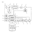
- Fig. 1 is a diagram showing a configuration example of an atomic absorption spectrophotometer according to an embodiment of the present invention.
- This atomic absorption spectrophotometer is a so-called furnace atomic absorption spectrophotometer, and is for generating atomic vapor by heating and atomizing a sample inside a graphite tube 2a, and measuring the absorbance of the sample by causing measurement light to pass through the atomic vapor.
- This atomic absorption spectrophotometer is provided with a light source 1, an atomizing unit 2, a spectroscope 3, a photomultiplier tube 4, an amplifier 5, an A/D converter 6, a control unit 7, a light source driving unit 8, a negative high voltage adjuster 9, an operation unit 10, a display unit 11, a memory 12, and the like.
- the light source 1 is provided with a hollow cathode lamp (HCL) 1a for radiating measurement light containing a bright line spectrum.
- the measurement light radiated from the hollow cathode lamp 1a passes through the graphite tube 2a provided to the atomizing unit 2.
- a sample solution is injected into the graphite tube 2a from a sample injection port (not shown), and the sample solution is heated by the graphite tube 2a through which a large current flows.
- the sample is thereby atomized, and atomic vapor is generated inside the graphite tube 2a.
- the measurement light has the light of a wavelength that is unique to the element contained in the sample greatly absorbed in the process of passing through the atomic vapor in the graphite tube 2a.
- the measurement light which has passed through the atomizing unit 2 enters the spectroscope 3.
- a diffraction grating is provided to the spectroscope 3, for example, and measurement light diffracted by the diffraction grating enters the photomultiplier tube 4.
- the photomultiplier tube 4 is an example of a detector for detecting measurement light, and outputs a signal according to the received intensity of the measurement light.
- the output signal from this photomultiplier tube 4 is amplified by the amplifier 5, and is then converted into a digital signal by the A/D converter 6 and input to the control unit 7.
- the control unit 7 is a structure including a CPU (Central Processing Unit), for example, and controls the operation of each unit provided to the atomic absorption spectrophotometer.
- the absorbance of the sample is measured based on the input signal from the A/D converter 6. Specifically, the absorbance is measured based on the ratio between the received intensity of measurement light when light is absorbed in the atomic vapor and the received intensity of measurement light when light is not absorbed.
- the atomizing unit 2, the amplifier 5, the light source driving unit 8, the negative high voltage adjuster 9, the operation unit 10, the display unit 11, the memory 12 and the like are electrically connected to the control unit 7.
- the light source driving unit 8 is for driving the hollow cathode lamp 1a provided to the light source 1, and outputs a drive signal to the hollow cathode lamp 1a based on a control signal from the control unit 7.
- the signal voltage of the photomultiplier tube 4 is dependent on the negative high voltage applied to the photomultiplier tube 4. Accordingly, by adjusting the negative high voltage to be applied to the photomultiplier tube 4 via the negative high voltage adjuster 9, the amplification factor of the signal voltage of the photomultiplier tube 4 may be adjusted. In the present embodiment, adjustment of the signal voltage is enabled by adjusting the amplification factor of the signal voltage of the photomultiplier tube 4 by the negative high voltage adjuster 9 after determining a signal level of a certain degree by circuit switching of the amplifier 5, and by performing control so as to bring the signal voltage closer to a set value (target value).
- the operation unit 10 is a structure including a keyboard or a mouse, for example, and an input task may be performed by an operator operating the operation unit 10.
- the display unit 11 may be configured from a liquid crystal display, for example, and results of processing by the control unit 7 and the like may be displayed on the display unit 11.
- the memory 12 may be configured from a ROM (Read Only Memory), a RAM (Random Access Memory) and the like, for example.
- the control unit 7 functions as a test measurement execution processing unit 7a, a signal voltage optimization processing unit 7b and the like by the CPU executing programs.
- test measurement of the sample is performed by the test measurement execution processing unit 7a, and a set value of the signal voltage of the photomultiplier tube 4 corresponding to the sample may be optimized based on the result of the test measurement.
- the test measurement execution processing unit 7a performs test measurement of the sample in a state where a preset value is taken as the set value of the signal voltage of the photomultiplier tube 4.
- the preset value is stored in the memory 12, and at the time of test measurement, this preset value is read from the memory 12, and is taken as the set value of the signal voltage of the photomultiplier tube 4.
- test measurement is performed in a state where control of bringing the signal voltage of the photomultiplier tube 4 close to the set value is performed, by atomizing the sample at the atomizing unit 2 and detecting, by the photomultiplier tube 4, measurement light which has passed through the generated atomic vapor.
- the preset value is desirably a value of 50% to 70% of the maximum value of the signal voltage of the photomultiplier tube 4. In the case where the maximum value of the signal voltage of the photomultiplier tube 4 is 2.5 V, the preset value may be set to 1.5 V, for example.
- the signal voltage optimization processing unit 7b optimizes the set value of the signal voltage of the photomultiplier tube 4 corresponding to a sample based on the signal voltage of the photomultiplier tube 4 at the time of test measurement of the sample. Specifically, if, as a result of the test measurement of the sample, it is determined that the signal voltage of the photomultiplier tube 4 may be saturated at the time of actual measurement, the set value of the signal voltage of the photomultiplier tube 4 corresponding to the sample is set to a lower value.
- the set value of the signal voltage of the photomultiplier tube 4 corresponding to the sample may be optimized based on the signal voltage of the photomultiplier tube 4 at the time of the test measurement. That is, the set value of the signal voltage of the photomultiplier tube 4 corresponding to a sample may be optimized through test measurement using the actual sample.
- the set value of the signal voltage of the photomultiplier tube 4 corresponding to the sample may be set to a value according to which the signal voltage is not saturated at the time of actual measurement. Accordingly, saturation of the signal voltage of the photomultiplier tube 4 at the time of measurement may be effectively prevented.
- the memory 12 configures a signal voltage storage unit that stores, in association with a sample, a set value of the signal voltage of the photomultiplier tube 4 which has been optimized by the signal voltage optimization processing unit 7b.
- a signal voltage storage unit that stores, in association with a sample, a set value of the signal voltage of the photomultiplier tube 4 which has been optimized by the signal voltage optimization processing unit 7b.
- Fig. 2 is a flow chart showing an example of processing by the control unit 7 at the time of test measurement.
- a value higher than the preset value is set in advance as the upper limit value of the signal voltage of the photomultiplier tube 4
- a value lower than the preset value is set in advance as the lower limit value of the set value of the signal voltage of the photomultiplier tube 4.
- the upper limit value of the signal voltage of the photomultiplier tube 4 refers to the maximum voltage at which the signal voltage is saturated and measurement cannot be normally performed, for example.
- the lower limit value of the set value of the signal voltage of the photomultiplier tube 4 refers to the minimum voltage which is such a value that if the set value is set to a value lower than that, the S/N ratio at the time of measurement is too low and measurement cannot be performed normally, for example.
- a preset value of the signal voltage of the photomultiplier tube 4 is read from the memory 12 (step S101). Then, test measurement of a sample is performed with the preset value taken as the set value of the signal voltage of the photomultiplier tube 4 (step S102).
- the preset value is determined to be the set value of the signal voltage of the photomultiplier tube 4 corresponding to the sample (step S104). At this time, the preset value is stored in the memory 12 in association with the sample, as the set value of the signal voltage of the photomultiplier tube 4 (step S107).
- step S105 whether or not the set value of the signal voltage of the photomultiplier tube 4 has reached the lower limit value is determined.
- the set value of the signal voltage of the photomultiplier tube 4 is the preset value, which is a value higher than the lower limit value, and thus, the set value of the signal voltage of the photomultiplier tube 4 has not reached the lower limit value (No in step S105).
- the set value of the signal voltage of the photomultiplier tube 4 is reset to a lower value (for example, a value that is one step lower) (step S108), and the test measurement of the sample is performed again using the set value (step S102). If, as a result, the signal voltage of the photomultiplier tube 4 at the time of the test measurement of the sample is below the upper limit value (Yes in step S103), the set value of the signal voltage of the photomultiplier tube 4 at this time is determined to be the set value of the signal voltage of the photomultiplier tube 4 corresponding to the sample (step S104), and this set value is stored in the memory 12 in association with the sample (step S107).
- a lower value for example, a value that is one step lower
- the test measurement of the sample may be performed several times until the signal voltage of the photomultiplier tube 4 at the time of the test measurement is below the upper limit value (until Yes is achieved in step S103).
- the set value of the signal voltage when the signal voltage of the photomultiplier tube 4 at the time of the test measurement falls below the upper limit value is determined to be the set value of the signal voltage of the photomultiplier tube 4 corresponding to the sample (step S104), and this set value is stored in the memory 12 in association with the sample (step S107).
- step S105 the test measurement of the sample is ended.
- an abnormality notification is issued by a display on the display unit 11 (step S106), for example, and the set value of the signal voltage of the photomultiplier tube 4 that is set in the test measurement of the sample at the time is stored in the memory 12 in association with the sample (step S107).
- steps S101, S102, and S108 in Fig. 2 constitute a test measurement execution processing step of performing test measurement of a sample.
- steps S103, S104, and S105 constitute a signal voltage optimization processing step of optimizing the set value of the signal voltage of the photomultiplier tube 4 corresponding to a sample.
- Step S107 constitutes a signal voltage storing step of storing an optimized set value of the signal voltage of the photomultiplier tube 4 in association with a sample.
- Step S106 constitutes an abnormality notification step of notifying an operator of an abnormal state.
- a normality notification step of notifying an operator of normal completion in the case where the set value of the signal voltage of the photomultiplier tube 4 is normally determined in step S104 may be included without being restricted to the abnormality notification step.
- the normality notification may be issued by a display on the display unit 11, for example.
- the preset value may be determined to be a value according to which the signal voltage of the photomultiplier tube 4 will not be saturated at the time of actual measurement, and be determined to be the set value corresponding to the sample (step S104).
- the preset value may be determined to be a value according to which the signal voltage of the photomultiplier tube 4 will possibly be saturated, and be reset to a lower value (step S108).
- the set value of the signal voltage at the time of the signal voltage of the photomultiplier tube 4 falling below the upper limit value may be determined to be a value according to which the signal voltage of the photomultiplier tube 4 will not be saturated at the time of actual measurement, and be determined to be the set value corresponding to the sample (step S104).
- the test measurement of the sample may be ended.
- conditions other than the signal voltage of the photomultiplier tube 4 for example, atomization conditions
- the test measurement of the sample is ended, and other appropriate measures may be taken.
- Fig. 3 is a diagram showing a configuration example of an atomic absorption spectrophotometer according to another embodiment.
- This atomic absorption spectrophotometer is a furnace atomic absorption spectrophotometer, as in the embodiment described above, but is a dual light source atomic absorption spectrophotometer including, at the light source 1, a deuterium lamp (D2L) 1b for radiating light including a continuous spectrum, in addition to the hollow cathode lamp 1a.
- D2L deuterium lamp
- This atomic absorption spectrophotometer is capable of performing so-called background correction using light from the deuterium lamp 1b. Structures other than that regarding the background correction are the same as the structures of the embodiment described above, and the same structures are denoted with the same reference signs in the drawing, and detailed description thereof is omitted.
- a semitransparent mirror 1c is provided to the light source 1, and measurement light radiated from the hollow cathode lamp 1a passes through the semitransparent mirror 1c and enters the graphite tube 2a of the atomizing unit 2.
- light from the deuterium lamp 1b is reflected by the semitransparent mirror 1c, and enters the graphite tube 2a of the atomizing unit 2 on the same axis as the measurement light from the hollow cathode lamp 1a.
- the hollow cathode lamp 1a and the deuterium lamp 1b are pulse-lighted under the control of the control unit 7 via the light source driving unit 8.
- the measurement light from the hollow cathode lamp 1a and the light from the deuterium lamp 1b are alternately detected by the photomultiplier tube 4 via the atomizing unit 2 and the spectroscope 3, and a time division multiplexed (TDM) signal is output from the photomultiplier tube 4.
- TDM time division multiplexed
- An output signal from the photomultiplier tube 4 has the high frequency noise removed by a low-pass filter (LPF) 13 after being amplified by the amplifier 5, and is input to a synchronous circuit 14.
- LPF low-pass filter
- an output signal of the photomultiplier tube 4 based on the measurement light from the hollow cathode lamp 1a and an output signal of the photomultiplier tube 4 based on the light from the deuterium lamp 1b are separated, and these output signals are input to the control unit 7 via the A/D converter 6.
- the measurement light from the hollow cathode lamp 1a may undergo absorption (background absorption) other than the original absorption at the atomizing unit 2.
- absorption background absorption
- the present embodiment also in such a case, by calculating the difference between the output signal of the photomultiplier tube 4 based on the measurement light from the hollow cathode lamp 1a and the output signal of the photomultiplier tube 4 based on the light from the deuterium lamp 1b, background correction may be performed, and the influence of background absorption may be eliminated.
- the present invention may also be applied to the dual light source atomic absorption spectrophotometer as described above.
- the difference between the set value, of the signal voltage of the photomultiplier tube 4 based on the measurement light, which is optimized by test measurement and the signal voltage of the photomultiplier tube 4 based on the light from the deuterium lamp 1b is desirably smaller.
- a structure is adopted according to which a variable dimmer 1d is provided to the light source 1 and the amount of light from the deuterium lamp 1b is adjusted, thereby making it possible to reduce the difference.
- a concrete example as shown in Fig. 2 is described as the method for optimizing the set value of the signal voltage of the photomultiplier tube 4.
- the method for optimizing the set value is not restricted to such a concrete example, and the set value may be optimized in various other modes.
- a configuration may be adopted according to which the set value is reset by an operator operating the operation unit 10, instead of being limited to a configuration where the set value of the signal voltage of the photomultiplier tube 4 is automatically reset to a lower value (step S108).
- the detector for detecting measurement light is not limited to the photomultiplier tube 4, and various other detectors may be adopted. Also, the light source for radiating the measurement light is not limited to the hollow cathode lamp 1a, and various other light sources may be adopted.
- the present invention is not limited to the furnace atomic absorption spectrophotometer, and may also be applied to, for example, a flame atomic absorption spectrophotometer that sprays a sample to a flammable gas and burns the mixture gas thereby heating and atomizing the sample, and that measures the absorbance of the sample by causing measurement light to pass through the generated atomic vapor.
Landscapes
- Physics & Mathematics (AREA)
- Spectroscopy & Molecular Physics (AREA)
- Health & Medical Sciences (AREA)
- Life Sciences & Earth Sciences (AREA)
- Chemical & Material Sciences (AREA)
- Analytical Chemistry (AREA)
- Biochemistry (AREA)
- General Health & Medical Sciences (AREA)
- General Physics & Mathematics (AREA)
- Immunology (AREA)
- Pathology (AREA)
- Engineering & Computer Science (AREA)
- Mathematical Physics (AREA)
- Theoretical Computer Science (AREA)
- Investigating Or Analysing Materials By Optical Means (AREA)
Abstract
Description
- The present invention relates to an atomic absorption spectrophotometer for causing measurement light to pass through atomic vapor generated by heating and atomizing a sample and detecting the measurement light by a detector to measure absorbance of the sample, and a signal voltage optimization method used by the same.
- An atomic absorption spectrophotometer is provided with an atomizing unit for heating and atomizing a sample. At the atomizing unit, a sample is atomized, thereby generating atomic vapor, and measurement light is radiated in the atomic vapor by a light source. At this time, light of a specific wavelength is absorbed in the atomic vapor, and thus, analysis of the sample may be performed by measuring the absorbance (for example, see
Patent Documents 1 and 2). - The measurement light which has passed through the atomic vapor is detected by a detector. The detector may be configured from a photomultiplier tube, for example. An output signal from the detector is amplified by an amplifier, and is then input to a control unit via an A/D converter. At the control unit, the absorbance is measured based on the ratio between the received intensity of measurement light when light is absorbed in the atomic vapor and the received intensity of measurement light when light is not absorbed.
- With a general atomic absorption spectrophotometer, light that reaches the detector includes, in addition to the measurement light from the light source as described above, light from outside the device, light occurring at the atomizing unit and the like, for example. As the light occurring at the atomizing unit, light emission from the structure of the atomizing unit accompanying heating, light emission from the sample itself and the like may be cited. Among these light emissions, light emission from the sample itself has a property that the amount of light emission is greater as the concentration of the sample is higher.
- With this type of atomic absorption spectrophotometer, depending on the measurement conditions, the amount of light emission from the structure of the atomizing unit accompanying heating may change, and a signal voltage of the detector (detector signal voltage) may exceed the maximum voltage that can be measured. Accordingly,
Patent Document 1 proposes a configuration for storing detector signal voltages for all the settable combinations of wavelengths, slit widths, and atomizing temperatures of the atomizing unit. Then, at the time of sample measurement, an amplifier is controlled by an optimum detector signal amplification factor based on the detector signal voltage stored in relation to the wavelength, the slit width, and the atomizing temperature used for the sample measurement. - However, even with the configuration in
Patent Document 1, depending on the measurement conditions (wavelength, slit width, flame species, gas flow rate), the detector signal voltage may exceed the maximum voltage that can be measured and accurate measurement is sometimes prevented. Thus,Patent Document 2 proposes a configuration for storing an optimal value of the detector signal voltage for an A/D converter corresponding to a combination of measurement conditions that may be simultaneously set. Then, when measurement conditions are set, a voltage adjustment section or a signal amplifier is adjusted so that the optimal value of a corresponding detector signal voltage is input to the A/D converter. -
- Patent Document 1:
JP 2004-325341 A - Patent Document 2:
JP 2007-10314 A - As described above, by optimizing the detector signal voltage or the amplification factor by taking measurement conditions into account, measurement may be normally performed in many cases. However, in the case where the concentration of a sample which is the analysis target is unexpectedly high, the amount of light emission from the sample itself may be unexpectedly great. Also, shifting of the optical axis of measurement light with respect to the atomizing unit caused by insufficient adjustment or the like may result in an unexpectedly great amount of light emission from the structure of the atomizing unit.
- In the case where the amount of light emission from the sample itself or the structure of the atomizing unit is unexpectedly great as described above, the detector signal voltage may be saturated, and measurement may not be normally performed. A set value of the detector signal voltage may be set low in advance taking into account of saturation of the detector signal voltage, but in this case, there is a problem that the SIN ratio at the time of measurement is reduced and the measurement accuracy is reduced.
- The present invention has been made in view of the above circumstances, and has its aim to provide an atomic absorption spectrophotometer capable of effectively preventing saturation of a signal voltage of a detector at the time of measurement, and a signal voltage optimization method used by the same.
- An atomic absorption spectrophotometer of the present invention is an atomic absorption spectrophotometer for causing measurement light to pass through atomic vapor generated by heating and atomizing a sample and detecting the measurement light by a detector to measure absorbance of the sample, the atomic absorption spectrophotometer comprising: a test measurement execution processing unit for performing test measurement of the sample in a state where a preset value is taken as a set value of a signal voltage of the detector; and a signal voltage optimization processing unit for optimizing, based on the signal voltage of the detector at a time of the test measurement of the sample, the set value of the signal voltage of the detector corresponding to the sample.
- According to the configuration described above, by performing test measurement of a sample, the set value of the signal voltage of the detector corresponding to the sample may be optimized based on the signal voltage of the detector at the time of the test measurement. That is, the set value of the signal voltage of the detector corresponding to the sample may be optimized through test measurement using the actual sample.
- Therefore, even in a case where the amount of light emission of the sample itself or of the structure of the atomizing unit is unexpectedly great, the set value of the signal voltage of the detector corresponding to the sample may be set to a value according to which the signal voltage is not saturated at the time of actual measurement. Accordingly, saturation of the signal voltage of the detector at the time of measurement may be effectively prevented.
- The atomic absorption spectrophotometer preferably further comprises a signal voltage storage unit for storing, in association with the sample, the set value of the signal voltage of the detector optimized by the signal voltage optimization processing unit.
- According to the configuration described above, by storing the optimized set value of the signal voltage of the detector in association with a sample, at the time of performing measurement of the same sample, measurement may be performed by reading the set value. Then, the efficiency of measurement may be increased, and also, saturation of the signal voltage of the detector at the time of measurement may be effectively prevented.
- In a case where the signal voltage of the detector at a time of the test measurement of the sample is below an upper limit value, the signal voltage optimization processing unit may determine the preset value to be the set value of the signal voltage of the detector corresponding to the sample.
- According to the configuration described above, in the case where the signal voltage of the detector is below the upper limit value at the time of test measurement of a sample where a preset value is taken as the set value of the signal voltage of the detector, the preset value may be determined to be a value according to which the signal voltage of the detector will not be saturated at the time of actual measurement, and be determined to be the set value corresponding to the sample.
- In a case where the signal voltage of the detector at a time of the test measurement of the sample is at or above an upper limit value, the test measurement execution processing unit may reset the set value of the signal voltage of the detector to a lower value, and perform again the test measurement of the sample. In this case, in a case where the test measurement of the sample is performed several times, the signal voltage optimization processing unit may determine the set value of the signal voltage when the signal voltage of the detector falls below the upper limit value to be the set value of the signal voltage of the detector corresponding to the sample.
- According to the configuration described above, in the case where the signal voltage of the detector is at or above the upper limit value at the time of test measurement of a sample where the preset value is taken as the set value of the signal voltage of the detector, the preset value may be determined to be a value according to which the signal voltage of the detector will possibly be saturated, and be reset to a lower value. When the set value of the signal voltage of the detector is reset in this manner, and the test measurement of the sample is performed several times, the set value of the signal voltage at the time of the signal voltage of the detector falling below the upper limit value may be determined to be a value according to which the signal voltage of the detector will not be saturated at the time of actual measurement, and be determined to be the set value corresponding to the sample.
- In a case where the set value of the signal voltage of the detector that is reset reaches a lower limit value, the test measurement execution processing unit may end the test measurement of the sample.
- According to the configuration described above, in the case where the set value reaches the lower limit value without the signal voltage of the detector falling below the upper limit value when the set value of the signal voltage of the detector is reset and test measurement of a sample is performed several times, the test measurement of the sample may be ended. In such a case, conditions other than the signal voltage of the detector have to be re-examined, and thus, the test measurement of the sample is ended, and other appropriate measures may be taken.
- A signal voltage optimization method of an atomic absorption spectrophotometer of the present invention is a method for optimizing a set value of a signal voltage of a detector in the atomic absorption spectrophotometer for causing measurement light to pass through atomic vapor generated by heating and atomizing a sample and detecting the measurement light by the detector to measure absorbance of the sample, the method comprising: a test measurement execution processing step of performing test measurement of the sample in a state where a preset value is taken as the set value of the signal voltage of the detector; and a signal voltage optimization processing step of optimizing, based on the signal voltage of the detector at a time of the test measurement of the sample, the set value of the signal voltage of the detector corresponding to the sample.
- The signal voltage optimization method preferably further comprises a signal voltage storage step of storing, in association with the sample, the set value of the signal voltage of the detector optimized in the signal voltage optimization processing step.
- In the signal voltage optimization processing step, in a case where the signal voltage of the detector at a time of the test measurement of the sample is below an upper limit value, the preset value may be determined to be the set value of the signal voltage of the detector corresponding to the sample.
- In the test measurement execution processing step, in a case where the signal voltage of the detector at a time of the test measurement of the sample is at or above an upper limit value, the set value of the signal voltage of the detector may be reset to a lower value, and the test measurement of the sample may be performed again. In this case, in the signal voltage optimization processing step, in a case where the test measurement of the sample is performed several times, the set value of the signal voltage when the signal voltage of the detector falls below the upper limit value may be determined to be the set value of the signal voltage of the detector corresponding to the sample.
- In the test measurement execution processing step, in a case where the set value of the signal voltage of the detector that is reset reaches a lower limit value, the test measurement of the sample may be ended.
- According to the present invention, by optimizing the set value of the signal voltage of the detector corresponding to a sample through test measurement using the actual sample, saturation of the signal voltage of the detector at the time of measurement may be effectively prevented.
-
-
Fig. 1 is a diagram showing a configuration example of an atomic absorption spectrophotometer according to an embodiment of the present invention; -
Fig. 2 is a flow chart showing an example of processing by a control unit at the time of test measurement; and -
Fig. 3 is a diagram showing a configuration example of an atomic absorption spectrophotometer according to another embodiment. -
Fig. 1 is a diagram showing a configuration example of an atomic absorption spectrophotometer according to an embodiment of the present invention. This atomic absorption spectrophotometer is a so-called furnace atomic absorption spectrophotometer, and is for generating atomic vapor by heating and atomizing a sample inside a graphite tube 2a, and measuring the absorbance of the sample by causing measurement light to pass through the atomic vapor. - This atomic absorption spectrophotometer is provided with a
light source 1, anatomizing unit 2, aspectroscope 3, aphotomultiplier tube 4, anamplifier 5, an A/D converter 6, acontrol unit 7, a lightsource driving unit 8, a negative high voltage adjuster 9, anoperation unit 10, adisplay unit 11, amemory 12, and the like. - The
light source 1 is provided with a hollow cathode lamp (HCL) 1a for radiating measurement light containing a bright line spectrum. The measurement light radiated from the hollow cathode lamp 1a passes through the graphite tube 2a provided to the atomizingunit 2. - A sample solution is injected into the graphite tube 2a from a sample injection port (not shown), and the sample solution is heated by the graphite tube 2a through which a large current flows. The sample is thereby atomized, and atomic vapor is generated inside the graphite tube 2a. The measurement light has the light of a wavelength that is unique to the element contained in the sample greatly absorbed in the process of passing through the atomic vapor in the graphite tube 2a.
- The measurement light which has passed through the
atomizing unit 2 enters thespectroscope 3. A diffraction grating is provided to thespectroscope 3, for example, and measurement light diffracted by the diffraction grating enters thephotomultiplier tube 4. Thephotomultiplier tube 4 is an example of a detector for detecting measurement light, and outputs a signal according to the received intensity of the measurement light. The output signal from thisphotomultiplier tube 4 is amplified by theamplifier 5, and is then converted into a digital signal by the A/D converter 6 and input to thecontrol unit 7. - The
control unit 7 is a structure including a CPU (Central Processing Unit), for example, and controls the operation of each unit provided to the atomic absorption spectrophotometer. At thecontrol unit 7, the absorbance of the sample is measured based on the input signal from the A/D converter 6. Specifically, the absorbance is measured based on the ratio between the received intensity of measurement light when light is absorbed in the atomic vapor and the received intensity of measurement light when light is not absorbed. - The
atomizing unit 2, theamplifier 5, the lightsource driving unit 8, the negative high voltage adjuster 9, theoperation unit 10, thedisplay unit 11, thememory 12 and the like are electrically connected to thecontrol unit 7. The lightsource driving unit 8 is for driving the hollow cathode lamp 1a provided to thelight source 1, and outputs a drive signal to the hollow cathode lamp 1a based on a control signal from thecontrol unit 7. - The signal voltage of the
photomultiplier tube 4 is dependent on the negative high voltage applied to thephotomultiplier tube 4. Accordingly, by adjusting the negative high voltage to be applied to thephotomultiplier tube 4 via the negative high voltage adjuster 9, the amplification factor of the signal voltage of thephotomultiplier tube 4 may be adjusted. In the present embodiment, adjustment of the signal voltage is enabled by adjusting the amplification factor of the signal voltage of thephotomultiplier tube 4 by the negative high voltage adjuster 9 after determining a signal level of a certain degree by circuit switching of theamplifier 5, and by performing control so as to bring the signal voltage closer to a set value (target value). - The
operation unit 10 is a structure including a keyboard or a mouse, for example, and an input task may be performed by an operator operating theoperation unit 10. Thedisplay unit 11 may be configured from a liquid crystal display, for example, and results of processing by thecontrol unit 7 and the like may be displayed on thedisplay unit 11. Thememory 12 may be configured from a ROM (Read Only Memory), a RAM (Random Access Memory) and the like, for example. - The
control unit 7 functions as a test measurement execution processing unit 7a, a signal voltageoptimization processing unit 7b and the like by the CPU executing programs. In the present embodiment, before actually measuring a sample, test measurement of the sample is performed by the test measurement execution processing unit 7a, and a set value of the signal voltage of thephotomultiplier tube 4 corresponding to the sample may be optimized based on the result of the test measurement. - The test measurement execution processing unit 7a performs test measurement of the sample in a state where a preset value is taken as the set value of the signal voltage of the
photomultiplier tube 4. The preset value is stored in thememory 12, and at the time of test measurement, this preset value is read from thememory 12, and is taken as the set value of the signal voltage of thephotomultiplier tube 4. Then, test measurement is performed in a state where control of bringing the signal voltage of thephotomultiplier tube 4 close to the set value is performed, by atomizing the sample at theatomizing unit 2 and detecting, by thephotomultiplier tube 4, measurement light which has passed through the generated atomic vapor. - Although not particularly restricted, the preset value is desirably a value of 50% to 70% of the maximum value of the signal voltage of the
photomultiplier tube 4. In the case where the maximum value of the signal voltage of thephotomultiplier tube 4 is 2.5 V, the preset value may be set to 1.5 V, for example. - The signal voltage
optimization processing unit 7b optimizes the set value of the signal voltage of thephotomultiplier tube 4 corresponding to a sample based on the signal voltage of thephotomultiplier tube 4 at the time of test measurement of the sample. Specifically, if, as a result of the test measurement of the sample, it is determined that the signal voltage of thephotomultiplier tube 4 may be saturated at the time of actual measurement, the set value of the signal voltage of thephotomultiplier tube 4 corresponding to the sample is set to a lower value. - In this manner, according to the present embodiment, by performing test measurement of a sample, the set value of the signal voltage of the
photomultiplier tube 4 corresponding to the sample may be optimized based on the signal voltage of thephotomultiplier tube 4 at the time of the test measurement. That is, the set value of the signal voltage of thephotomultiplier tube 4 corresponding to a sample may be optimized through test measurement using the actual sample. - Thus, even in a case where the amount of light emission of the sample itself or of the structure of the
atomizing unit 2 is unexpectedly great, the set value of the signal voltage of thephotomultiplier tube 4 corresponding to the sample may be set to a value according to which the signal voltage is not saturated at the time of actual measurement. Accordingly, saturation of the signal voltage of thephotomultiplier tube 4 at the time of measurement may be effectively prevented. - In the present embodiment, the
memory 12 configures a signal voltage storage unit that stores, in association with a sample, a set value of the signal voltage of thephotomultiplier tube 4 which has been optimized by the signal voltageoptimization processing unit 7b. By storing an optimized set value of the signal voltage of thephotomultiplier tube 4 in association with a sample as described above, at the time of performing measurement of the same sample, measurement may be performed by reading the set value. Then, the efficiency of measurement may be increased, and also, saturation of the signal voltage of thephotomultiplier tube 4 at the time of measurement may be effectively prevented. -
Fig. 2 is a flow chart showing an example of processing by thecontrol unit 7 at the time of test measurement. In the present embodiment, a value higher than the preset value is set in advance as the upper limit value of the signal voltage of thephotomultiplier tube 4, and a value lower than the preset value is set in advance as the lower limit value of the set value of the signal voltage of thephotomultiplier tube 4. - Additionally, the upper limit value of the signal voltage of the
photomultiplier tube 4 refers to the maximum voltage at which the signal voltage is saturated and measurement cannot be normally performed, for example. Also, the lower limit value of the set value of the signal voltage of thephotomultiplier tube 4 refers to the minimum voltage which is such a value that if the set value is set to a value lower than that, the S/N ratio at the time of measurement is too low and measurement cannot be performed normally, for example. - At the time of performing test measurement of a sample, first, a preset value of the signal voltage of the
photomultiplier tube 4 is read from the memory 12 (step S101). Then, test measurement of a sample is performed with the preset value taken as the set value of the signal voltage of the photomultiplier tube 4 (step S102). - In the case where the signal voltage of the
photomultiplier tube 4 at the time of the test measurement of the sample is below the upper limit value (Yes in step S103), the preset value is determined to be the set value of the signal voltage of thephotomultiplier tube 4 corresponding to the sample (step S104). At this time, the preset value is stored in thememory 12 in association with the sample, as the set value of the signal voltage of the photomultiplier tube 4 (step S107). - On the other hand, in the case where the signal voltage of the
photomultiplier tube 4 at the time of the test measurement of the sample is at or above the upper limit value (No in step S103), whether or not the set value of the signal voltage of thephotomultiplier tube 4 has reached the lower limit value is determined (step S105). At this point, the set value of the signal voltage of thephotomultiplier tube 4 is the preset value, which is a value higher than the lower limit value, and thus, the set value of the signal voltage of thephotomultiplier tube 4 has not reached the lower limit value (No in step S105). - In this case, the set value of the signal voltage of the
photomultiplier tube 4 is reset to a lower value (for example, a value that is one step lower) (step S108), and the test measurement of the sample is performed again using the set value (step S102). If, as a result, the signal voltage of thephotomultiplier tube 4 at the time of the test measurement of the sample is below the upper limit value (Yes in step S103), the set value of the signal voltage of thephotomultiplier tube 4 at this time is determined to be the set value of the signal voltage of thephotomultiplier tube 4 corresponding to the sample (step S104), and this set value is stored in thememory 12 in association with the sample (step S107). - The test measurement of the sample (step S102) may be performed several times until the signal voltage of the
photomultiplier tube 4 at the time of the test measurement is below the upper limit value (until Yes is achieved in step S103). In the case where the test measurement of the sample is performed several times in this manner, the set value of the signal voltage when the signal voltage of thephotomultiplier tube 4 at the time of the test measurement falls below the upper limit value is determined to be the set value of the signal voltage of thephotomultiplier tube 4 corresponding to the sample (step S104), and this set value is stored in thememory 12 in association with the sample (step S107). - However, if the set value of the signal voltage of the
photomultiplier tube 4 that is reset reaches the lower limit value (Yes in step S105) before the signal voltage of thephotomultiplier tube 4 at the time of the test measurement of the sample falls below the upper limit value (before Yes is achieved in step S103), the test measurement of the sample is ended. In this case, an abnormality notification is issued by a display on the display unit 11 (step S106), for example, and the set value of the signal voltage of thephotomultiplier tube 4 that is set in the test measurement of the sample at the time is stored in thememory 12 in association with the sample (step S107). - In the present embodiment, steps S101, S102, and S108 in
Fig. 2 constitute a test measurement execution processing step of performing test measurement of a sample. Steps S103, S104, and S105 constitute a signal voltage optimization processing step of optimizing the set value of the signal voltage of thephotomultiplier tube 4 corresponding to a sample. Step S107 constitutes a signal voltage storing step of storing an optimized set value of the signal voltage of thephotomultiplier tube 4 in association with a sample. - Step S106 constitutes an abnormality notification step of notifying an operator of an abnormal state. Incidentally, for example, a normality notification step of notifying an operator of normal completion in the case where the set value of the signal voltage of the
photomultiplier tube 4 is normally determined in step S104 may be included without being restricted to the abnormality notification step. In this case, the normality notification may be issued by a display on thedisplay unit 11, for example. - As described above, in the present embodiment, in the case where the signal voltage of the
photomultiplier tube 4 is below the upper limit value at the time of test measurement of a sample where a preset value is taken as the set value of the signal voltage of the photomultiplier tube 4 (Yes in step S103), the preset value may be determined to be a value according to which the signal voltage of thephotomultiplier tube 4 will not be saturated at the time of actual measurement, and be determined to be the set value corresponding to the sample (step S104). - On the other hand, in the case where the signal voltage of the
photomultiplier tube 4 is at or above the upper limit value at the time of test measurement of a sample where the preset value is taken as the set value of the signal voltage of the photomultiplier tube 4 (No in step S103), the preset value may be determined to be a value according to which the signal voltage of thephotomultiplier tube 4 will possibly be saturated, and be reset to a lower value (step S108). In the case where the set value of the signal voltage of thephotomultiplier tube 4 is reset in the above manner, and the test measurement of the sample is performed several times, the set value of the signal voltage at the time of the signal voltage of thephotomultiplier tube 4 falling below the upper limit value (at the time when Yes is achieved in step S103) may be determined to be a value according to which the signal voltage of thephotomultiplier tube 4 will not be saturated at the time of actual measurement, and be determined to be the set value corresponding to the sample (step S104). - Also, in the case where the set value reaches the lower limit value without the signal voltage of the
photomultiplier tube 4 falling below the upper limit value when the set value of the signal voltage of thephotomultiplier tube 4 is reset and test measurement of the sample is performed several times (Yes in step S105), the test measurement of the sample may be ended. In such a case, conditions other than the signal voltage of the photomultiplier tube 4 (for example, atomization conditions) have to be re-examined, and thus, the test measurement of the sample is ended, and other appropriate measures may be taken. -
Fig. 3 is a diagram showing a configuration example of an atomic absorption spectrophotometer according to another embodiment. This atomic absorption spectrophotometer is a furnace atomic absorption spectrophotometer, as in the embodiment described above, but is a dual light source atomic absorption spectrophotometer including, at thelight source 1, a deuterium lamp (D2L) 1b for radiating light including a continuous spectrum, in addition to the hollow cathode lamp 1a. - This atomic absorption spectrophotometer is capable of performing so-called background correction using light from the deuterium lamp 1b. Structures other than that regarding the background correction are the same as the structures of the embodiment described above, and the same structures are denoted with the same reference signs in the drawing, and detailed description thereof is omitted.
- A semitransparent mirror 1c is provided to the
light source 1, and measurement light radiated from the hollow cathode lamp 1a passes through the semitransparent mirror 1c and enters the graphite tube 2a of theatomizing unit 2. On the other hand, light from the deuterium lamp 1b is reflected by the semitransparent mirror 1c, and enters the graphite tube 2a of theatomizing unit 2 on the same axis as the measurement light from the hollow cathode lamp 1a. - The hollow cathode lamp 1a and the deuterium lamp 1b are pulse-lighted under the control of the
control unit 7 via the lightsource driving unit 8. The measurement light from the hollow cathode lamp 1a and the light from the deuterium lamp 1b are alternately detected by thephotomultiplier tube 4 via theatomizing unit 2 and thespectroscope 3, and a time division multiplexed (TDM) signal is output from thephotomultiplier tube 4. - An output signal from the
photomultiplier tube 4 has the high frequency noise removed by a low-pass filter (LPF) 13 after being amplified by theamplifier 5, and is input to asynchronous circuit 14. At thesynchronous circuit 14, an output signal of thephotomultiplier tube 4 based on the measurement light from the hollow cathode lamp 1a and an output signal of thephotomultiplier tube 4 based on the light from the deuterium lamp 1b are separated, and these output signals are input to thecontrol unit 7 via the A/D converter 6. - Depending on the type of the sample, the measurement conditions or the like, the measurement light from the hollow cathode lamp 1a may undergo absorption (background absorption) other than the original absorption at the
atomizing unit 2. According to the present embodiment, also in such a case, by calculating the difference between the output signal of thephotomultiplier tube 4 based on the measurement light from the hollow cathode lamp 1a and the output signal of thephotomultiplier tube 4 based on the light from the deuterium lamp 1b, background correction may be performed, and the influence of background absorption may be eliminated. - The present invention may also be applied to the dual light source atomic absorption spectrophotometer as described above. However, in this case, the difference between the set value, of the signal voltage of the
photomultiplier tube 4 based on the measurement light, which is optimized by test measurement and the signal voltage of thephotomultiplier tube 4 based on the light from the deuterium lamp 1b is desirably smaller. Accordingly, in the present embodiment, a structure is adopted according to which a variable dimmer 1d is provided to thelight source 1 and the amount of light from the deuterium lamp 1b is adjusted, thereby making it possible to reduce the difference. - In the embodiment described above, a concrete example as shown in
Fig. 2 is described as the method for optimizing the set value of the signal voltage of thephotomultiplier tube 4. However, the method for optimizing the set value is not restricted to such a concrete example, and the set value may be optimized in various other modes. - For example, in the case where the signal voltage of the
photomultiplier tube 4 at the time of test measurement of a sample is at or above the upper limit value (No in step S103), a configuration may be adopted according to which the set value is reset by an operator operating theoperation unit 10, instead of being limited to a configuration where the set value of the signal voltage of thephotomultiplier tube 4 is automatically reset to a lower value (step S108). - The detector for detecting measurement light is not limited to the
photomultiplier tube 4, and various other detectors may be adopted. Also, the light source for radiating the measurement light is not limited to the hollow cathode lamp 1a, and various other light sources may be adopted. - Also, the present invention is not limited to the furnace atomic absorption spectrophotometer, and may also be applied to, for example, a flame atomic absorption spectrophotometer that sprays a sample to a flammable gas and burns the mixture gas thereby heating and atomizing the sample, and that measures the absorbance of the sample by causing measurement light to pass through the generated atomic vapor.
-
- 1
- light source
- 1a
- hollow cathode lamp
- 1b
- deuterium lamp
- 1c
- semitransparent mirror
- 1d
- variable dimmer
- 2
- atomizing unit
- 2a
- graphite tube
- 3
- spectroscope
- 4
- photomultiplier tube
- 5
- amplifier
- 6
- A/D converter
- 7
- control unit
- 7a
- test measurement execution processing unit
- 7b
- signal voltage optimization processing unit
- 8
- light source driving unit
- 9
- negative high voltage adjuster
- 10
- operation unit
- 11
- display unit
- 12
- memory
- 13
- low-pass filter
- 14
- synchronous circuit
Claims (10)
- An atomic absorption spectrophotometer for causing measurement light to pass through atomic vapor generated by heating and atomizing a sample and detecting the measurement light by a detector to measure absorbance of the sample, the atomic absorption spectrophotometer comprising:a test measurement execution processing unit for performing test measurement of the sample in a state where a preset value is taken as a set value of a signal voltage of the detector; anda signal voltage optimization processing unit for optimizing, based on the signal voltage of the detector at a time of the test measurement of the sample, the set value of the signal voltage of the detector corresponding to the sample.
- The atomic absorption spectrophotometer according to claim 1, further comprising a signal voltage storage unit for storing, in association with the sample, the set value of the signal voltage of the detector optimized by the signal voltage optimization processing unit.
- The atomic absorption spectrophotometer according to claim 1 or 2, wherein, in a case where the signal voltage of the detector at a time of the test measurement of the sample is below an upper limit value, the signal voltage optimization processing unit determines the preset value to be the set value of the signal voltage of the detector corresponding to the sample.
- The atomic absorption spectrophotometer according to any one of claims 1 to 3,
wherein, in a case where the signal voltage of the detector at a time of the test measurement of the sample is at or above an upper limit value, the test measurement execution processing unit resets the set value of the signal voltage of the detector to a lower value, and performs again the test measurement of the sample, and
wherein, in a case where the test measurement of the sample is performed several times, the signal voltage optimization processing unit determines the set value of the signal voltage when the signal voltage of the detector falls below the upper limit value to be the set value of the signal voltage of the detector corresponding to the sample. - The atomic absorption spectrophotometer according to claim 4, wherein, in a case where the set value of the signal voltage of the detector that is reset reaches a lower limit value, the test measurement execution processing unit ends the test measurement of the sample.
- A signal voltage optimization method of an atomic absorption spectrophotometer, the method being for optimizing a set value of a signal voltage of a detector in the atomic absorption spectrophotometer for causing measurement light to pass through atomic vapor generated by heating and atomizing a sample and detecting the measurement light by the detector to measure absorbance of the sample, the method comprising:a test measurement execution processing step of performing test measurement of the sample in a state where a preset value is taken as the set value of the signal voltage of the detector; anda signal voltage optimization processing step of optimizing, based on the signal voltage of the detector at a time of the test measurement of the sample, the set value of the signal voltage of the detector corresponding to the sample.
- The signal voltage optimization method of the atomic absorption spectrophotometer according to claim 6, further comprising a signal voltage storage step of storing, in association with the sample, the set value of the signal voltage of the detector optimized in the signal voltage optimization processing step.
- The signal voltage optimization method of the atomic absorption spectrophotometer according to claim 6 or 7, wherein, in the signal voltage optimization processing step, in a case where the signal voltage of the detector at a time of the test measurement of the sample is below an upper limit value, the preset value is determined to be the set value of the signal voltage of the detector corresponding to the sample.
- The signal voltage optimization method of the atomic absorption spectrophotometer according to any one of claims 6 to 8,
wherein, in the test measurement execution processing step, in a case where the signal voltage of the detector at a time of the test measurement of the sample is at or above an upper limit value, the set value of the signal voltage of the detector is reset to a lower value, and the test measurement of the sample is performed again, and
wherein, in the signal voltage optimization processing step, in a case where the test measurement of the sample is performed several times, the set value of the signal voltage when the signal voltage of the detector falls below the upper limit value is determined to be the set value of the signal voltage of the detector corresponding to the sample. - The signal voltage optimization method of the atomic absorption spectrophotometer according to claim 9, wherein, in the test measurement execution processing step, in a case where the set value of the signal voltage of the detector that is reset reaches a lower limit value, the test measurement of the sample is ended.
Applications Claiming Priority (1)
| Application Number | Priority Date | Filing Date | Title |
|---|---|---|---|
| PCT/JP2012/078603 WO2014068781A1 (en) | 2012-11-05 | 2012-11-05 | Atomic absorption spectrophotometer and signal voltage optimization method used in same |
Publications (2)
| Publication Number | Publication Date |
|---|---|
| EP2927667A1 true EP2927667A1 (en) | 2015-10-07 |
| EP2927667A4 EP2927667A4 (en) | 2016-06-29 |
Family
ID=50626744
Family Applications (1)
| Application Number | Title | Priority Date | Filing Date |
|---|---|---|---|
| EP12887346.0A Withdrawn EP2927667A4 (en) | 2012-11-05 | 2012-11-05 | Atomic absorption spectrophotometer and signal voltage optimization method used in same |
Country Status (5)
| Country | Link |
|---|---|
| US (1) | US9874514B2 (en) |
| EP (1) | EP2927667A4 (en) |
| JP (1) | JP5975109B2 (en) |
| CN (1) | CN104769416B (en) |
| WO (1) | WO2014068781A1 (en) |
Families Citing this family (4)
| Publication number | Priority date | Publication date | Assignee | Title |
|---|---|---|---|---|
| JP6825708B2 (en) * | 2017-07-10 | 2021-02-03 | 株式会社島津製作所 | Frame type atomic absorption spectrophotometer |
| CN111380651A (en) * | 2018-12-29 | 2020-07-07 | 株式会社岛津制作所 | State indication method of detection instrument, device, medium and system thereof |
| DE102019103035A1 (en) * | 2019-02-07 | 2020-08-13 | Analytik Jena Ag | Atomic absorption spectrometer |
| CN115943300B (en) * | 2020-08-24 | 2025-12-05 | 株式会社岛津制作所 | Atomic absorption spectrophotometer and its control method |
Family Cites Families (12)
| Publication number | Priority date | Publication date | Assignee | Title |
|---|---|---|---|---|
| JPS5255686A (en) * | 1975-10-31 | 1977-05-07 | Seiko Instr & Electronics Ltd | Computer controlled atomic absorption spectrophotometer |
| JPS59125040A (en) * | 1982-12-30 | 1984-07-19 | Shimadzu Corp | Spectroscopic analyzer |
| JP3461982B2 (en) * | 1995-09-21 | 2003-10-27 | 株式会社日立製作所 | Atomic absorption photometer |
| US6043880A (en) * | 1997-09-15 | 2000-03-28 | Becton Dickinson And Company | Automated optical reader for nucleic acid assays |
| JP2001153799A (en) * | 1999-11-29 | 2001-06-08 | Shimadzu Corp | Quantitative analysis method and quantitative analyzer |
| JP2003523510A (en) * | 2000-02-15 | 2003-08-05 | ベアリアン・オーストラリア・プロプライエタリー・リミテッド | Method and apparatus for spectroscopic analysis |
| US6809804B1 (en) * | 2000-05-11 | 2004-10-26 | Becton, Dickinson And Company | System and method for providing improved event reading and data processing capabilities in a flow cytometer |
| US6870166B2 (en) | 2002-02-28 | 2005-03-22 | Agilent Technologies, Inc. | Maximum sensitivity optical scanning system |
| JP3960256B2 (en) * | 2003-04-25 | 2007-08-15 | 株式会社島津製作所 | Atomic absorption spectrophotometer |
| JP2007010314A (en) | 2005-06-28 | 2007-01-18 | Shimadzu Corp | Flame atomic absorption spectrophotometer |
| US8184286B2 (en) * | 2006-12-18 | 2012-05-22 | Shimadzu Corporation | Atomic absorption spectrophotometer |
| JP5251729B2 (en) * | 2008-06-20 | 2013-07-31 | 株式会社島津製作所 | Spectrophotometer |
-
2012
- 2012-11-05 CN CN201280076870.6A patent/CN104769416B/en not_active Expired - Fee Related
- 2012-11-05 WO PCT/JP2012/078603 patent/WO2014068781A1/en not_active Ceased
- 2012-11-05 EP EP12887346.0A patent/EP2927667A4/en not_active Withdrawn
- 2012-11-05 US US14/437,754 patent/US9874514B2/en not_active Expired - Fee Related
- 2012-11-05 JP JP2014544192A patent/JP5975109B2/en not_active Expired - Fee Related
Also Published As
| Publication number | Publication date |
|---|---|
| JP5975109B2 (en) | 2016-08-23 |
| EP2927667A4 (en) | 2016-06-29 |
| CN104769416A (en) | 2015-07-08 |
| US9874514B2 (en) | 2018-01-23 |
| US20150293014A1 (en) | 2015-10-15 |
| WO2014068781A1 (en) | 2014-05-08 |
| CN104769416B (en) | 2018-01-09 |
| JPWO2014068781A1 (en) | 2016-09-08 |
Similar Documents
| Publication | Publication Date | Title |
|---|---|---|
| US9874514B2 (en) | Atomic absorption spectrophotometer and signal voltage optimization method used by the same | |
| US9829430B2 (en) | Spectrophotometer | |
| JP3960256B2 (en) | Atomic absorption spectrophotometer | |
| US12078624B2 (en) | Spectrophotometer | |
| US8717557B2 (en) | Spectrophotometer and method for determining performance thereof | |
| JP6201547B2 (en) | Spectrometer wavelength calibration method | |
| US10184886B2 (en) | Atomic absorption photometer and atomic absorption measurement method | |
| JP6167920B2 (en) | Spectrophotometer | |
| JPH01224645A (en) | Atomic absorption spectrophotometer | |
| JPWO2019043858A1 (en) | Atomic absorption spectrophotometer and atomic absorption measurement method | |
| CN111829971A (en) | Method for reducing measurement error of wide spectrum transmittance | |
| JP2024078963A (en) | Wavelength calibration method and atomic absorption spectrophotometer | |
| JP2007010314A (en) | Flame atomic absorption spectrophotometer | |
| Schorsch et al. | Detection of flame radicals using light-emitting diodes | |
| JP5895691B2 (en) | Solar cell evaluation apparatus and method | |
| CN115943300B (en) | Atomic absorption spectrophotometer and its control method | |
| JP2003185498A (en) | Spectrophotometer | |
| JP2013234895A (en) | Solar cell evaluating device and method | |
| JP2014102146A (en) | Spectrophotometer | |
| CN121207894A (en) | Spectrophotometer, spectral analysis method and spectral analysis procedure | |
| JP6128737B2 (en) | Tunable monochromatic light source | |
| CN121632992A (en) | Spectrophotometer, spectrophotometric measurement methods and procedures | |
| JP2017161318A (en) | Analyzer | |
| JP2004286764A (en) | Molten metal analysis method | |
| JP2007024684A (en) | Automatic analyzer |
Legal Events
| Date | Code | Title | Description |
|---|---|---|---|
| PUAI | Public reference made under article 153(3) epc to a published international application that has entered the european phase |
Free format text: ORIGINAL CODE: 0009012 |
|
| 17P | Request for examination filed |
Effective date: 20150501 |
|
| AK | Designated contracting states |
Kind code of ref document: A1 Designated state(s): AL AT BE BG CH CY CZ DE DK EE ES FI FR GB GR HR HU IE IS IT LI LT LU LV MC MK MT NL NO PL PT RO RS SE SI SK SM TR |
|
| AX | Request for extension of the european patent |
Extension state: BA ME |
|
| DAX | Request for extension of the european patent (deleted) | ||
| RA4 | Supplementary search report drawn up and despatched (corrected) |
Effective date: 20160527 |
|
| RIC1 | Information provided on ipc code assigned before grant |
Ipc: G01N 21/31 20060101AFI20160520BHEP |
|
| 17Q | First examination report despatched |
Effective date: 20181026 |
|
| STAA | Information on the status of an ep patent application or granted ep patent |
Free format text: STATUS: THE APPLICATION HAS BEEN WITHDRAWN |
|
| 18W | Application withdrawn |
Effective date: 20190301 |