EP2924525A1 - Method of inspecting ram of programmable logic controller, and programmable logic controller - Google Patents
Method of inspecting ram of programmable logic controller, and programmable logic controller Download PDFInfo
- Publication number
- EP2924525A1 EP2924525A1 EP15160240.6A EP15160240A EP2924525A1 EP 2924525 A1 EP2924525 A1 EP 2924525A1 EP 15160240 A EP15160240 A EP 15160240A EP 2924525 A1 EP2924525 A1 EP 2924525A1
- Authority
- EP
- European Patent Office
- Prior art keywords
- ram
- unit storage
- blocks
- region
- storage regions
- Prior art date
- Legal status (The legal status is an assumption and is not a legal conclusion. Google has not performed a legal analysis and makes no representation as to the accuracy of the status listed.)
- Withdrawn
Links
Images




Classifications
-
- G—PHYSICS
- G05—CONTROLLING; REGULATING
- G05B—CONTROL OR REGULATING SYSTEMS IN GENERAL; FUNCTIONAL ELEMENTS OF SUCH SYSTEMS; MONITORING OR TESTING ARRANGEMENTS FOR SUCH SYSTEMS OR ELEMENTS
- G05B19/00—Program-control systems
- G05B19/02—Program-control systems electric
- G05B19/04—Program control other than numerical control, i.e. in sequence controllers or logic controllers
- G05B19/05—Programmable logic controllers, e.g. simulating logic interconnections of signals according to ladder diagrams or function charts
- G05B19/058—Safety, monitoring
-
- G—PHYSICS
- G05—CONTROLLING; REGULATING
- G05B—CONTROL OR REGULATING SYSTEMS IN GENERAL; FUNCTIONAL ELEMENTS OF SUCH SYSTEMS; MONITORING OR TESTING ARRANGEMENTS FOR SUCH SYSTEMS OR ELEMENTS
- G05B2219/00—Program-control systems
- G05B2219/10—Plc systems
- G05B2219/14—Plc safety
- G05B2219/14085—Memory testing
-
- G—PHYSICS
- G11—INFORMATION STORAGE
- G11C—STATIC STORES
- G11C29/00—Checking stores for correct operation ; Subsequent repair; Testing stores during standby or offline operation
- G11C29/04—Detection or location of defective memory elements, e.g. cell constructio details, timing of test signals
- G11C2029/0409—Online test
Definitions
- the present invention relates to a method of inspecting a RAM of a programmable logic controller, and to a programmable logic controller.
- a programmable logic controller (hereinafter referred to as "PLC”) is used to control automated machinery in a factory or the like.
- the PLC includes a central processing unit (hereinafter referred to as "CPU") that is a small computer and that executes a program.
- CPU central processing unit
- a ladder diagram that simulates a ladder circuit is used to prepare the program. The ladder diagram may be rewritten as appropriate into a sequence program that matches the usage.
- the PLC receives a signal (on or off information) about a continuity state input from a variety of input devices (such as switches and sensors).
- the PLC controls (e.g. outputs an on or off signal to) output devices (such as relays and motors) with the sequence program in which the variety of input devices are combined in a desired form (connected in series or in parallel).
- a safety standard for a random access memory that is abbreviated as "RAM” and that is a memory that enables data to be read from and written into a desired address at any time
- a method called Galpat may be used to inspect the RAM in order to meet the safety standard for the RAM.
- Galpat inspecting the RAM using the Galpat takes a significantly long time (e.g. about two to three hours), and it takes much time to detect an abnormality of the RAM, which is not preferable.
- JP 8-87429 A describes a method of inspecting an application program storage region (ROM region) of a PLC for performing sequence control that is changed in accordance with the usage, in which a check sum (inspection reference value) obtained by totaling program codes in a region to be inspected is stored in the ROM in advance. To execute the inspection, it is determined whether or not a value obtained by totaling values read from the ROM as the region to be inspected coincides with the check sum stored in the ROM.
- JP 2006-40122 A describes an inspection method in which a RAM region of a PLC to be inspected is divided into a plurality of regions, one inspection unit is inspected each time the PLC is turned on, and an inspection unit that is next to the inspection unit inspected before the PLC is turned off the last time is inspected when the PLC is turned on again after the PLC is turned off.
- JP 8-87429 A The inspection method described in JP 8-87429 A is intended to inspect program codes stored in the ROM, not to inspect the RAM, which enables values to be rewritten at any time, and may not be applied to the inspection of the RAM.
- a method of inspecting a RAM of a programmable logic controller including:
- the writing and reading step is executed for all combinations of two blocks extracted from the blocks obtained by dividing the RAM inspection region, and thus it is possible to inspect the RAM in a short time and to appropriately meet a predetermined safety standard (such as the IEC standard).
- a predetermined safety standard such as the IEC standard
- the RAM may be provided with a RAM temporary saving region which is different from the RAM inspection region; the number of unit storage regions in each block may be set to be equal to or less than half the number of unit storage regions in the RAM temporary saving region; and the control device may execute the writing and reading step after values in unit storage regions in the extracted combination of blocks are stored in the RAM temporary saving region, and write the values stored in the RAM temporary saving region back into the respective original unit storage regions in the combination of blocks after execution of the writing and reading step so that the values stored in the RAM inspection region before inspection of the RAM are reproduced and maintained after inspection of the RAM.
- the RAM inspection program uses the method of inspecting a RAM of a programmable logic controller according to above mentioned aspect to inspect the unit storage regions in the RAM inspection region.
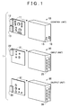
- a PLC 1 is composed of a control unit 10, an input unit 20, and an output unit 30. Extra input units 20 and output units 30 may be added as appropriate in accordance with the number of inputs and outputs.
- An input board 21 that includes a connector 22 for connection with the control unit 10 is housed in the input unit 20.
- the input unit 20 is provided with an input terminal 25 for connection with wiring that extends from a plurality of input devices (such as switches and sensors).
- An output board 31 that includes a connector 33 for connection with the control unit 10 is housed in the output unit 30.
- the output unit 30 is provided with an output terminal 35 for connection with wiring that extends to a plurality of output devices (such as relays and motors).
- a control board 11 that includes a connector 12 for connection with the input unit 20 and a connector 13 for connection with the output unit 30 is housed in the control unit 10.
- the control unit 10 is provided with a connector 15 for connection with a terminal device such as a personal computer, a connector 16 for connection with another PLC, and so forth.
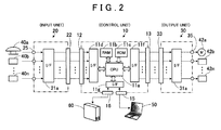
- Wiring that extends from a plurality of input devices (such as a switch 40a, a sensor 40b through an input device 40n) is connected to the input terminal 25 of the input unit 20.
- a signal (such as on or off information) about a continuity state of the input devices is input to the input terminal 25.
- the input signal about the continuity state is transferred to the control unit 10 via an interface 21a (the term “interface” is hereinafter referred to as "I/F”) and the connector 22.
- the control unit 10 is mainly composed of a CPU 11a (corresponding to the control device), and includes a RAM 11b and a ROM 11c.
- a rewritable ROM such as an EEPROM or a flash ROM is used as the ROM 11c.
- the ROM 11c stores a sequence program that simulates a sequence circuit constituted by connecting desired input devices in series or in parallel, and so forth.
- a user can use the terminal device 50 to prepare a sequence program using a ladder circuit or the like, and can have the prepared sequence program stored in (written into) the control unit 10.
- a RAM inspection program that implements a RAM inspection method to be discussed later is implemented in the sequence program.
- the ROM 11c also stores a program for communication with the terminal device 50, another PLC 60, or the like via an I/F 11g, and so forth.
- the CPU 11a outputs a computation result based on the sequence program stored in the ROM 11c and the signal about the continuity state from the input devices input from the input unit 20 via the connector 12 and an I/F 11d to the output unit 30 via an I/F 11f and the connector 13.
- Wiring that extends to a plurality of output devices (such as a motor 42a, a relay 42b through an output device 42n) is connected to the output terminal 35 of the output unit 30.
- a computation result obtained by the control unit 10 on the basis of the sequence program and the continuity state of the input devices is output to the output devices connected to the output terminal 35 via the connector 33 and an I/F 31a.
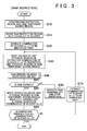
- the RAM inspection illustrated in FIG. 3 is invoked by an interrupt process or the like while the control unit 10 is executing normal control, that is, a machine control process called a main process or a normal process.
- the timing to invoke the RAM inspection is not specifically limited.
- the process procedure of the RAM inspection method described in relation to the embodiment is based on a known memory testing method called "March C".
- the RAM inspection region is the entire region excluding special use regions such as a stack region, a communication region, and regions for peripheral devices.
- step S10 the CPU 11a confirms a RAM inspection region as a region of the RAM to be inspected and a RAM temporary saving region, and the process proceeds to step S15.
- the start address and last address of the RAM inspection region, the start address and last address of the RAM temporary saving region, and so forth are stored in advance somewhere in the program region of the ROM 11c.
- the RAM inspection region is located at addresses 0x00 to 0xBF
- the RAM temporary saving region is located at addresses 0xC0 to 0xFF.
- the start and last addresses of such regions are stored in the ROM 11c, and the CPU 11a reads such addresses from the ROM 11c to confirm the RAM inspection region and the RAM temporary saving region.
- the RAM temporary saving region may be a stack region, for example.
- the RAM inspection region is a region at continuous addresses.
- the RAM inspection region is not limited to a region at continuous addresses, and may be a plurality of non-continuous regions.
- step S15 the CPU 11a divides the RAM inspection region into a plurality of blocks, and the process proceeds to step S20.
- the RAM inspection region is divided into blocks such that the number of unit storage regions in each block is equal to or less than half the number of unit storage regions in the RAM temporary saving region.
- unit storage region refers to a minimum storage region for writing and reading data, and may be a one-byte storage region, for example. Different addresses are assigned to each unit storage region. In the case of the example of the region configuration of the RAM of FIG.
- the inspection time can be made shorter as the number of divided blocks is smaller.
- the RAM inspection region is divided such that the number of unit storage regions in each block is 32, and the RAM inspection region is divided into first to sixth blocks.
- the RAM inspection region may be divided into blocks in advance to omit steps S10 and S15.
- step S20 the CPU 11a extracts a combination of blocks (m, n) to be inspected first from combinations of blocks (such as a combination of the first block and the second block and a combination of the third block and the fourth block, for example) obtained by combining two blocks extracted from the divided blocks, and the process proceeds to step S35.
- (m, n) is equal to (1, 2) in the case where a combination of the first block and the second block is extracted
- (m, n) is equal to (3, 4) in the case where a combination of the third block and the fourth block is extracted.
- the combination of blocks to be inspected first may be a combination of blocks (1, 2).
- (m, n) indicates a combination of the m-th block and the n-th block (m ⁇ n).
- step S35 the CPU 11a copies (saves) values of unit storage regions in the extracted combination of blocks (m, n) to respective unit storage regions in the RAM temporary saving region, and the process proceeds to step S40.
- (m, n) is equal to (1, 2)
- values of unit storage regions (addresses 0x00 to 0x1F) in the first block illustrated in FIG. 8 are copied to respective unit storage regions (addresses 0xC0 to 0xDF) in the RAM temporary saving region
- values of unit storage regions (addresses 0x20 to Ox3F) in the second block are copied to respective unit storage regions (addresses 0xE0 to 0xFF) in the RAM temporary saving region.
- step S40 the CPU 11a executes a process of a sub routine SB 100 illustrated in FIGS. 4 to 7 .
- the process proceeds to step S50.
- a predetermined value is written into each unit storage region in the extracted combination of blocks (m, n), and thereafter it is sequentially inspected whether or not a value read from the unit storage region coincides with the written value.
- the process of the sub routine SB 100 corresponds towriting and reading step, and will be discussed in detail later.
- step S50 the CPU 11a determines whether or not the RAM is normal as a result of the process of the sub routine SB 100. In the case where the RAM is normal (Yes), the process proceeds to step S60. In the case where the RAM is not normal (No), the process proceeds to step S80. In step S80, the CPU 11a indicates (e.g. turns on an abnormality lamp) that an abnormality of the RAM has been found, and stops operation.
- step S60 the CPU 11a writes the copied values in the unit storage regions in the RAM temporary saving region (the value copied in step S35) back into the original unit storage regions in the extracted combination of blocks (m, n), and the process proceeds to step S65.
- (m, n) is equal to (1, 2)
- the copied (saved) values in the unit storage regions (addresses 0xC0 to 0xDF) in the RAM temporary saving region illustrated in FIG. 8 are written back into the original unit storage regions (addresses 0x00 to 0x1F) in the first block, and the copied
- step S65 the CPU 11a determines whether or not inspection of all the combinations of blocks (m, n) has been finished. In the case where inspection of all the combinations of blocks has been finished (Yes), the process of the RAM inspection is ended. In the case where inspection of all the combinations of blocks has not been finished (No), the process proceeds to step S70. For example, in the case where the RAM inspection region is divided into first to sixth blocks as illustrated in FIG.
- step S70 the CPU 11a extracts a combination of blocks (m, n) to be inspected next, and the process returns to step S35.
- step S70 is reached when the combination of blocks (1, 2) has been inspected, the next combination of blocks (1, 3) is extracted, and the process returns to step S35.
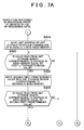
- the process procedure illustrated in FIG. 4 is a RAM writing/reading inspection executed in the ascending order of the address of the unit storage regions by use of ascending data (values) to be written and read.
- the process procedure illustrated in FIG. 5 is a RAM writing/reading inspection executed in the ascending order of the address of the unit storage regions bv use of descending data (values) to be written and read.
- the process procedure illustrated in FIG. 6 is a RAM writing/reading inspection executed in the descending order of the address of the unit storage regions by use of ascending data (values) to be written and read.
- the process procedure illustrated in FIG. 7 is a RAM writing/reading inspection executed in the descending order of the address of the unit storage regions by use of descending data (values) to be written and read.
- step S110 illustrated in FIG. 4 the CPU 11a writes a first-first predetermined value into all the unit storage regions in the combination of blocks (m, n) in the ascending order of the address, and the process proceeds to step S115.
- the combination of blocks (1,2) for example, 0x00 as the first-first predetermined value is first written into the unit storage region at the address 0x00, and 0x00 (first-first predetermined value) is written into the unit storage region at the address 0x01 which is the next in the ascending order. After that, 0x00 (first-first predetermined value) is sequentially written into the unit storage regions at addresses of up to 0x3F.
- step S115 the CPU 11a saves the start address of the unit storage regions in the combination of blocks (m, n) (in this case, the start address of the unit storage regions is 0x00) into an index value storage region (hereinafter referred to as "index memory"), and the process proceeds to step S125.
- step S125 the CPU 11a reads a value from the unit storage region corresponding to the address in the index memory, and determines whether or not the read value coincides with the first-first predetermined value (the value written in step S110). In the case where such values coincide with each other (Yes), the process proceeds to step S130. In the case where such values do not coincide with each other (No), the process proceeds to step S180. In the case where the process proceeds to step S180, an abnormality of the RAM has been found, and the CPU 11a stores a RAM abnormality, and the process returns from the sub routine SB 100.
- step S130 the CPU 11a writes a first-second predetermined value which is the next in ascending order into the unit storage region corresponding to the address in the index memory, and the process proceeds to step S135.
- the first-second predetermined value may be 0x01, for example.
- step S135 the CPU 11a reads a value from the unit storage region corresponding to the address in the index memory, and determines whether or not the read value coincides with the first-second predetermined value (the value written in step S130). In the case where such values coincide with each other (Yes), the process proceeds to step S140. In the case where such values do not coincide with each other (No), the process proceeds to step S180.
- steps S135 and S140 steps in which a predetermined value is written into the unit storage region corresponding to the address in the index memory and it is checked whether or not the read value is the predetermined value using ascending data, namely, a first-third predetermined value (e.g. 0x03), a first-fourth predetermined value (e.g. 0x07), a first-fifth predetermined value (e.g. 0x0F), a first-sixth predetermined value (e.g. 0x1F), a first-seventh predetermined value (e.g. Ox3F), and a first-eighth predetermined value (e.g. Ox7F).
- a first-third predetermined value e.g. 0x03
- a first-fourth predetermined value e.g. 0x07
- a first-fifth predetermined value e.g. 0x0F
- a first-sixth predetermined value e.g. 0x1
- step S140 the CPU 11a writes a first-a-th predetermined value (e.g. 0xFF) into the unit storage region corresponding to the address in the index memory, and the process proceeds to step S145.
- step S145 the CPU 11a reads a value from the unit storage region corresponding to the address in the index memory, and determines whether or not the read value coincides with the first-a-th predetermined value (the value written in step S140). In the case where such values coincide with each other (Yes), the process proceeds to step S150. In the case where such values do not coincide with each other (No), the process proceeds to step S180. In the case where the process proceeds to step S180, as discussed above, the CPU 11a stores a RAM abnormality, and the process returns from the sub routine SB 100.
- a first-a-th predetermined value e.g. 0xFF
- the CPU 11a determines whether or not the address in the index memory is the last address of the unit storage regions in the combination of blocks (m, n) that is currently checked. In the case where the address in the index memory is the last address of the unit storage regions (Yes), the process proceeds to the process of FIG. 5 which corresponds to symbol B. In the case where the address in the index memory is not the last address of the unit storage regions (No), the process proceeds to step S155. For example, in the case of the combination of blocks (1, 2) (the first block and the second block) illustrated in FIG. 8 , the CPU 11a determines that the address in the index memory is the last address of the unit storage regions if the address in the index memory is 0x3F.
- the CPU 11a saves into the index memory the address of the unit storage region to be inspected next in the combination of blocks (m, n) that is currently extracted , and the process returns to step S125.
- the combination of blocks (1, 2) is currently extracted and the unit storage region at 0x00 has been checked
- 0x01 which is the address of the unit storage region to be inspected next is saved into the index memory since the inspection is performed in the ascending order of the address of the unit storage regions in the process of FIG. 4 .
- the RAM writing/reading inspection executed in the ascending order of the address of the unit storage regions by use of the ascending of data (values) to be written and read is completed through the process procedure illustrated in FIG. 4 . Subsequently, the RAM writing/reading inspection executed in the ascending order of the address of the unit storage regions by use of the descending data (values) to be written and read is executed through the process procedure illustrated in FIG. 5 .
- steps S215 to S280 illustrated in FIG. 5 are the same as the processes illustrated in FIG. 4 in that the unit storage regions in the same combination of blocks (m, n) are checked in the ascending order of the address, but are different from such processes in that data to be written and read are descending data rather than ascending data.
- step S215 is the same as the process in step S115 of FIG. 4 , and thus is not described.
- the process in step S225 is different from the process in step S125 of FIG. 4 in that the read value is the first-a-th predetermined value (which is the value written in step S140, e.g. 0xFF).
- the read value coincides with the first-a-th predetermined value (Yes)
- the process proceeds to step S230.
- step S280 In the case where the read value does not coincide with the first-a-th predetermined value, the process proceeds to step S280.
- the CPU 11a stores a RAM abnormality, and the process returns from the sub routine SB 100.
- steps S230 to S245 are different from the processes in steps S130 to S 145 of FIG. 4 in that the values to be written and read are descending values rather than ascending values. That is, in steps S130 to S145 of FIG. 4 , ascending data are written and read , namely in the order of the first-second predetermined value (0x01), the first-third predetermined value (0x03), the first-fourth predetermined value (0x07) through the first-a-th predetermined value (OxFF). In the processes in steps S230 to S245, however, descending data are written and read, namely in the order of a second-first predetermined value (e.g. 0xFE), a second-second predetermined value (e.g.
- a second-first predetermined value e.g. 0xFE
- a second-second predetermined value e.g.
- 0xFC a second-third predetermined value
- a second-fourth predetermined value e.g. 0xF0
- a second-fifth predetermined value e.g. 0xE0
- a second-sixth predetermined value e.g. 0xC0
- a second-seventh predetermined value e.g. 0x80
- a second-b-th predetermined value e.g. 0x00
- step S250 the CPU 11a determines whether or not the address in the index memory is the last address of the unit storage regions in the combination of blocks (m, n) that is currently checked. In the case where the address in the index memory is the last address of the unit storage regions (Yes), the process proceeds to the process of FIG. 6 indicated by symbol C. In the case where the address in the index memory is not the last address of the unit storage regions (No), the process proceeds to step S255.
- the CPU 11a saves into the index memory the address of the unit storage region to be inspected next in the combination of blocks (m, n) that is currently extracted , and the process returns to step S225.
- the combination of blocks (1, 2) is currently extracted and the unit storage region at 0x00 has been checked
- 0x01 which is the address of the unit storage region to be inspected next is saved into the index memory since the inspection is performed in the ascending order of the address of the unit storage regions in the process of FIG. 5 .
- the RAM writing/reading inspection executed in the ascending order of the address of the unit storage regions by use of the descending data (values) to be written and read is completed through the process procedure illustrated in FIG. 5 . Subsequently, a RAM writing/reading inspection executed in the descending order of the address of the unit storage regions by use of the ascending data (values) to be written and read is executed through the process procedure illustrated in FIG. 6 .
- steps S305 to S380 illustrated in FIG. 6 are different from the processes illustrated in FIG. 4 in that the unit storage regions in the same combination of blocks (m, n) are checked in the descending order of the address, but are the same as such processes in that data to be written and read are ascending data.
- step S305 the CPU 11a sequentially reads values from all the unit storage regions in the combination of blocks (m, n) (e.g. reads values in the ascending order of the address of the unit storage regions), and determines whether or not the read values each coincide with the second-b-th predetermined value (0x00). In the case where such values coincide with each other (Yes), the process proceeds to step S315. In the case where such values do not coincide with each other (No), the process proceeds to step S380. In the case where the process proceeds to step S380, the CPU 11a stores a RAM abnormality, and the process returns from the sub routine SB 100.
- step S315 the CPU 11a saves into the index memory the last address of the unit storage regions in the combination of blocks (m, n) (in this case, the last address of the unit storage regions is 0x3F), and the process proceeds to step S325.
- step S325 the CPU 11a reads a value from the unit storage region corresponding to the address in the index memory, and determines whether or not the read value coincides with the second-b-th predetermined value (the value written in step S240). In the case where such values coincide with each other (Yes), the process proceeds to step S330. In the case where such values do not coincide with each other (No), the process proceeds to step S380.
- step S380 the CPU 11a stores a RAM abnormality, and the process returns from the sub routine SB 100.
- steps S330 to S345 are the same as the processes in steps S130 to S145 in that the values to be written and read are ascending values, but are different from such processes in that the value in the index memory is varied in the descending order from the last address of the unit storage regions to the start address of the unit storage regions.
- Ascending data are written and read, namely in the order of the first-second predetermined value (0x01), the first-third predetermined value (0x03), the first-fourth predetermined value (0x07) through the first-a-th predetermined value (OxFF).
- the CPU 11a determines whether or not the address in the index memory is the start address of the unit storage regions in the combination of blocks (m, n) that is currently checked. In the case where the address in the index memory is the start address of the unit storage regions (Yes), the process proceeds to the process of FIG. 7 indicated by symbol D. In the case where the address in the index memory is not the start address of the unit storage regions (No), the process proceeds to step S355. In the case of the combination of blocks (1, 2) (the first block and the second block) illustrated in FIG. 8 , the CPU 11a determines that the address in the index memory is the start address of the unit storage regions if the address in the index memory is 0x00.
- step S355 the CPU 11a saves into the index memory the address of the unit storage region to be inspected next in the combination of blocks (m, n) that is currently extracted , and the process returns to step S325.
- the combination of blocks (1, 2) is currently extracted and the unit storage region at Ox3F has been checked
- Ox3E which is the address of the unit storage region to be inspected next is saved into the index memory since the inspection is performed in the descending order of the address of the unit storage regions in the process of FIG. 6 .
- the RAM writing/reading inspection executed in the descending order of the address of the unit storage regions by use of the ascending data (values) to be written and read is completed through the process procedure illustrated in FIG. 6 . Subsequently, the RAM writing/reading inspection executed in the descending order of the address of the unit storage regions by use of the descending data (values) to be written and read is executed through the process procedure illustrated in FIG. 7 .
- steps S415 to S490 illustrated in FIG. 7 are the same as the processes illustrated in FIG. 6 in that the unit storage regions in the same combination of blocks (m, n) are checked in the descending order of the address, but are different from such processes in that data to be written and read are descending data rather than ascending data.
- step S415 is the same as the process in step S315 of FIG. 6 , and thus is not described.
- the process in step S425 is different from the process in step S325 of FIG. 6 in that the read value is the first-a-th predetermined value (which is the value written in step S340, e.g. 0xFF).
- the read value coincides with the first-a-th predetermined value (Yes)
- the process proceeds to step S430.
- step S480 In the case where the read value does not coincide with the first-a-th predetermined value, the process proceeds to step S480.
- the CPU 11a stores a RAM abnormality, and the process returns from the sub routine SB 100.
- steps S430 to S445 are different from the processes in steps S330 to S345 of FIG. 6 in that the values to be written and read are descending values rather than ascending values.
- steps S330 to S345 of FIG. 6 ascending data are written and read, namely in the order of the first-second predetermined value (0x01), the first-third predetermined value (0x03), the first-fourth predetermined value (0x07) through the first-a-th predetermined value (OxFF).
- descending data are written and read, namely in the order of the second-first predetermined value (e.g. 0xFE), the second-second predetermined value (e.g.
- the second-third predetermined value e.g. 0xF8
- the second-fourth predetermined value e.g. 0xF0
- the second-fifth predetermined value e.g. 0xE0
- the second-sixth predetermined value e.g. 0xC0
- the second-seventh predetermined value e.g. 0x80
- the second-b-th predetermined value e.g. 0x00
- step S450 the CPU 11a determines whether or not the address in the index memory is the start address of the unit storage regions in the combination of blocks (m, n) that is currently checked. In the case where the address in the index memory is the start address of the unit storage regions (Yes), the CPU 11a proceeds to step S490. In the case where the address in the index memory is not the start address of the unit storage regions (No), the process proceeds to step S455.
- step S455 the CPU 11a saves into the index memory the address of the unit storage region to be inspected next in the combination of blocks (m, n) that is currently extracted , and the process returns to step S425.
- the combination of blocks (1, 2) is currently extracted and the unit storage region at Ox3F has been checked
- Ox3E which is the address of the unit storage region to be inspected next is saved into the index memory since the inspection is performed in the descending order of the address of the unit storage regions in the process of FIG. 7 .
- the RAM writing/reading inspection executed in the descending order of the address of the unit storage regions by use of the descending data (values) to be written and read is completed through the process procedure illustrated in FIG. 7 .
- the RAM is normal for all the unit storage regions in the extracted combination of blocks (m, n) in all of the RAM inspection performed in the ascending order of the address by use of the ascending data illustrated in FIG. 4 , the RAM inspection performed in the ascending order of the address by use of descending data illustrated in FIG. 5 , the RAM inspection performed in the descending order of the address by use of the ascending data illustrated in FIG. 6 , and the RAM inspection performed in the descending order of the address by use of the descending data illustrated in FIG. 7 .
- the CPU 11a stores a RAM normality, and the process returns from the sub routine SB 100.
- RAM interference refers to a phenomenon in which when data in a unit storage region at a first address are rewritten, data in a unit storage region at a second address that is different from the first address are also changed.
- the RAM inspection method described in relation to the embodiment it is possible to appropriately inspect whether unit storage regions in the entire RAM inspection region are normal in a short time and to meet a predetermined safety standard by dividing the RAM inspection region into a plurality of blocks, for example, and inspecting all combinations of two blocks even in the case where the size of the RAM inspection region is so large that there is no RAM temporary saving region that is sized enough to temporarily save the values of all the unit storage regions in the RAM inspection region.
- a method of inspecting a RAM of a programmable logic controller that enables all unit storage regions in a RAM inspection region to be inspected in about several minutes and that meets a predetermined safety standard.
- the inspection method includes the steps of: dividing step (S15) for dividing a RAM inspection region, which is a region of the RAM (11b) to be inspected, into a plurality of blocks; and writing and reading step (S40) for, by a control device, writing a predetermined value into unit storage regions in a combination of blocks obtained by combining two blocks extracted from the divided blocks and thereafter sequentially inspecting whether or not values read from the unit storage regions each coincide with the written value.
- the writing and reading step is executed for all combinations of two blocks extracted from the divided blocks.
Landscapes
- Physics & Mathematics (AREA)
- General Physics & Mathematics (AREA)
- Engineering & Computer Science (AREA)
- Automation & Control Theory (AREA)
- For Increasing The Reliability Of Semiconductor Memories (AREA)
- Programmable Controllers (AREA)
- Techniques For Improving Reliability Of Storages (AREA)
Abstract
A method of inspecting a RAM of a programmable logic controller is provided that enables all unit storage regions in a RAM inspection region to be inspected in about several minutes and that meets a predetermined safety standard. The inspection method includes the steps of: dividing step (S15) for dividing a RAM inspection region, which is a region of the RAM (11b) to be inspected, into a plurality of blocks; and writing and reading step (S40) for, by a control device, writing a predetermined value into unit storage regions in a combination of blocks obtained by combining two blocks extracted from the divided blocks and thereafter sequentially inspecting whether or not values read from the unit storage regions each coincide with the written value. The writing and reading step is executed for all combinations of two blocks extracted from the divided blocks.
Description
- The present invention relates to a method of inspecting a RAM of a programmable logic controller, and to a programmable logic controller.
- A programmable logic controller (hereinafter referred to as "PLC") is used to control automated machinery in a factory or the like. The PLC includes a central processing unit (hereinafter referred to as "CPU") that is a small computer and that executes a program. A ladder diagram that simulates a ladder circuit is used to prepare the program. The ladder diagram may be rewritten as appropriate into a sequence program that matches the usage. The PLC receives a signal (on or off information) about a continuity state input from a variety of input devices (such as switches and sensors). The PLC controls (e.g. outputs an on or off signal to) output devices (such as relays and motors) with the sequence program in which the variety of input devices are combined in a desired form (connected in series or in parallel).
- It is necessary that the PLC used in a factory or the like should meet a predetermined safety standard (e.g. the IEC standard). Among such safety standards, there is provided a safety standard for a random access memory (that is abbreviated as "RAM" and that is a memory that enables data to be read from and written into a desired address at any time) used by the CPU. A variety of methods have been considered to inspect the RAM in order to meet the safety standard for the RAM. For example, a method called Galpat may be used to inspect the RAM in order to meet the safety standard for the RAM. However, inspecting the RAM using the Galpat takes a significantly long time (e.g. about two to three hours), and it takes much time to detect an abnormality of the RAM, which is not preferable.
- Japanese Patent Application Publication No.
8-87429 JP 8-87429 A - Japanese Patent Application Publication No.
2006-40122 JP 2006-40122 A - The inspection method described in
JP 8-87429 A - In the inspection method described in
JP 2006-40122 A - It is an object of the present invention to provide a method of inspecting a RAM of a programmable logic controller that enables all unit storage regions in a RAM inspection region to be inspected in about several minutes and that appropriately meets a predetermined safety standard, and a programmable logic controller.
- According to an aspect of the present invention, a method of inspecting a RAM of a programmable logic controller, including:
- dividing step for dividing a RAM inspection region, which is a region of the RAM to be inspected, into a plurality of blocks; and
- writing and reading step for, by using a control device, writing a predetermined value into unit storage regions in a combination of blocks obtained by combining two blocks extracted from the divided blocks and thereafter sequentially inspecting whether or not values read from the unit storage regions each coincide with the written value. In the method, the control device executes the writing and reading step for all combinations of two blocks extracted from the divided blocks.
- According to above mentioned aspect, the writing and reading step is executed for all combinations of two blocks extracted from the blocks obtained by dividing the RAM inspection region, and thus it is possible to inspect the RAM in a short time and to appropriately meet a predetermined safety standard (such as the IEC standard).
- In the method of inspecting a RAM of a programmable logic controller according to above mentioned aspect , the RAM may be provided with a RAM temporary saving region which is different from the RAM inspection region;
the number of unit storage regions in each block may be set to be equal to or less than half the number of unit storage regions in the RAM temporary saving region; and
the control device may execute the writing and reading step after values in unit storage regions in the extracted combination of blocks are stored in the RAM temporary saving region, and write the values stored in the RAM temporary saving region back into the respective original unit storage regions in the combination of blocks after execution of the writing and reading step so that the values stored in the RAM inspection region before inspection of the RAM are reproduced and maintained after inspection of the RAM. - According to above mentioned aspect, it is possible to set the size of each of the divided blocks to an appropriate size, and to appropriately hold the value in the unit storage regions in the RAM inspection region before inspection of the RAM even after inspection of the RAM.
- According to above mentioned aspect of the present invention, in a programmable logic controller in which a RAM inspection program is installed, the RAM inspection program uses the method of inspecting a RAM of a programmable logic controller according to above mentioned aspect to inspect the unit storage regions in the RAM inspection region.
- According to above mentioned aspect, it is possible to provide a programmable logic controller that allows the RAM to be inspected appropriately in a short time.
- The foregoing and further features and advantages of the invention will become apparent from the following description of example embodiments with reference to the accompanying drawings, wherein like numerals are used to represent like elements and wherein:
-
FIG. 1 is a perspective view illustrating an example of the appearance of a control unit, an input unit, and an output unit that compose a PLC according to the present invention; -
FIG. 2 illustrates an example of the block configuration and the connection of the PLC composed of the control unit, the input unit, and the output unit; -
FIG. 3 is a flowchart illustrating the procedure of a process for inspecting a RAM performed by a CPU of the PLC; -
FIG. 4 is a flowchart illustrating the details of a process of a RAM writing/reading sub routine (SB 100) in the flowchart ofFIG. 3 ; -
FIG. 5 is a flowchart that follows the flowchart ofFIG. 4 ; -
FIG. 6 is a flowchart that follows the flowchart ofFIG. 5 ; -
FIG. 7 is a flowchart that follows the flowchart ofFIG. 6 ; and -
FIG. 8 illustrates an example of the configuration of a RAM region including a RAM inspection region to be inspected. - An embodiment of the present invention will be described below with reference to the drawings. As illustrated in
FIG. 1 , aPLC 1 is composed of acontrol unit 10, aninput unit 20, and anoutput unit 30.Extra input units 20 andoutput units 30 may be added as appropriate in accordance with the number of inputs and outputs. Aninput board 21 that includes aconnector 22 for connection with thecontrol unit 10 is housed in theinput unit 20. Theinput unit 20 is provided with aninput terminal 25 for connection with wiring that extends from a plurality of input devices (such as switches and sensors). Anoutput board 31 that includes aconnector 33 for connection with thecontrol unit 10 is housed in theoutput unit 30. Theoutput unit 30 is provided with anoutput terminal 35 for connection with wiring that extends to a plurality of output devices (such as relays and motors). Acontrol board 11 that includes aconnector 12 for connection with theinput unit 20 and aconnector 13 for connection with theoutput unit 30 is housed in thecontrol unit 10. Thecontrol unit 10 is provided with aconnector 15 for connection with a terminal device such as a personal computer, aconnector 16 for connection with another PLC, and so forth. - Next, an example of the block configuration and the connection of the
PLC 1 will be described with reference toFIG. 2 . Wiring that extends from a plurality of input devices (such as aswitch 40a, asensor 40b through aninput device 40n) is connected to theinput terminal 25 of theinput unit 20. A signal (such as on or off information) about a continuity state of the input devices is input to theinput terminal 25. The input signal about the continuity state is transferred to thecontrol unit 10 via aninterface 21a (the term "interface" is hereinafter referred to as "I/F") and theconnector 22. - The
control unit 10 is mainly composed of aCPU 11a (corresponding to the control device), and includes a RAM 11b and aROM 11c. A rewritable ROM such as an EEPROM or a flash ROM is used as theROM 11c. TheROM 11c stores a sequence program that simulates a sequence circuit constituted by connecting desired input devices in series or in parallel, and so forth. A user can use theterminal device 50 to prepare a sequence program using a ladder circuit or the like, and can have the prepared sequence program stored in (written into) thecontrol unit 10. A RAM inspection program that implements a RAM inspection method to be discussed later is implemented in the sequence program. TheROM 11c also stores a program for communication with theterminal device 50, anotherPLC 60, or the like via an I/F 11g, and so forth. TheCPU 11a outputs a computation result based on the sequence program stored in theROM 11c and the signal about the continuity state from the input devices input from theinput unit 20 via theconnector 12 and an I/F 11d to theoutput unit 30 via an I/F 11f and theconnector 13. - Wiring that extends to a plurality of output devices (such as a
motor 42a, a relay 42b through anoutput device 42n) is connected to theoutput terminal 35 of theoutput unit 30. A computation result obtained by thecontrol unit 10 on the basis of the sequence program and the continuity state of the input devices is output to the output devices connected to theoutput terminal 35 via theconnector 33 and an I/F 31a. - Next, the procedure of a process for inspecting the RAM 11b performed by the
CPU 11a (corresponding to the control device) of thecontrol unit 10 of thePLC 1 illustrated inFIG. 2 will be described with reference toFIG. 3 . The RAM inspection illustrated inFIG. 3 is invoked by an interrupt process or the like while thecontrol unit 10 is executing normal control, that is, a machine control process called a main process or a normal process. The timing to invoke the RAM inspection is not specifically limited. The process procedure of the RAM inspection method described in relation to the embodiment is based on a known memory testing method called "March C". In addition, the RAM inspection region is the entire region excluding special use regions such as a stack region, a communication region, and regions for peripheral devices. - In step S10, the
CPU 11a confirms a RAM inspection region as a region of the RAM to be inspected and a RAM temporary saving region, and the process proceeds to step S15. The start address and last address of the RAM inspection region, the start address and last address of the RAM temporary saving region, and so forth are stored in advance somewhere in the program region of theROM 11c. In the example illustrated inFIG. 8 , for example, the RAM inspection region is located at addresses 0x00 to 0xBF, and the RAM temporary saving region is located at addresses 0xC0 to 0xFF. (A number starting with "Ox" represents hexadecimal number.) The start and last addresses of such regions are stored in theROM 11c, and theCPU 11a reads such addresses from theROM 11c to confirm the RAM inspection region and the RAM temporary saving region. In addition, for the values in the RAM inspection region, it is necessary that the value stored before execution of the RAM inspection program should be maintained (held) also after execution of the RAM inspection program. The RAM temporary saving region may be a stack region, for example. In the example ofFIG. 8 , the RAM inspection region is a region at continuous addresses. However, the RAM inspection region is not limited to a region at continuous addresses, and may be a plurality of non-continuous regions. - In step S15, the
CPU 11a divides the RAM inspection region into a plurality of blocks, and the process proceeds to step S20. The RAM inspection region is divided into blocks such that the number of unit storage regions in each block is equal to or less than half the number of unit storage regions in the RAM temporary saving region. The term "unit storage region" refers to a minimum storage region for writing and reading data, and may be a one-byte storage region, for example. Different addresses are assigned to each unit storage region. In the case of the example of the region configuration of the RAM ofFIG. 8 , the RAM temporary saving region has 64 unit storage regions located over addresses of 0xC0 to 0xFF (Ox indicates a hexadecimal number), and thus the RAM inspection region is divided such that the number of unit storage regions in each block is equal to or less than 32 (=64*1/2). The inspection time can be made shorter as the number of divided blocks is smaller. Thus, in the example ofFIG. 8 , the RAM inspection region is divided such that the number of unit storage regions in each block is 32, and the RAM inspection region is divided into first to sixth blocks. The RAM inspection region may be divided into blocks in advance to omit steps S10 and S15. - In step S20, the
CPU 11a extracts a combination of blocks (m, n) to be inspected first from combinations of blocks (such as a combination of the first block and the second block and a combination of the third block and the fourth block, for example) obtained by combining two blocks extracted from the divided blocks, and the process proceeds to step S35. For example, (m, n) is equal to (1, 2) in the case where a combination of the first block and the second block is extracted, and (m, n) is equal to (3, 4) in the case where a combination of the third block and the fourth block is extracted. For example, the combination of blocks to be inspected first may be a combination of blocks (1, 2). In the following description, (m, n) indicates a combination of the m-th block and the n-th block (m < n). - In step S35, the
CPU 11a copies (saves) values of unit storage regions in the extracted combination of blocks (m, n) to respective unit storage regions in the RAM temporary saving region, and the process proceeds to step S40. In the case where (m, n) is equal to (1, 2), for example, values of unit storage regions (addresses 0x00 to 0x1F) in the first block illustrated inFIG. 8 are copied to respective unit storage regions (addresses 0xC0 to 0xDF) in the RAM temporary saving region, and values of unit storage regions (addresses 0x20 to Ox3F) in the second block are copied to respective unit storage regions (addresses 0xE0 to 0xFF) in the RAM temporary saving region. - In step S40, the
CPU 11a executes a process of asub routine SB 100 illustrated inFIGS. 4 to 7 . Returning from thesub routine SB 100, the process proceeds to step S50. In thesub routine SB 100, as discussed later, a predetermined value is written into each unit storage region in the extracted combination of blocks (m, n), and thereafter it is sequentially inspected whether or not a value read from the unit storage region coincides with the written value. The process of thesub routine SB 100 corresponds towriting and reading step, and will be discussed in detail later. - In step S50, the
CPU 11a determines whether or not the RAM is normal as a result of the process of thesub routine SB 100. In the case where the RAM is normal (Yes), the process proceeds to step S60. In the case where the RAM is not normal (No), the process proceeds to step S80. In step S80, theCPU 11a indicates (e.g. turns on an abnormality lamp) that an abnormality of the RAM has been found, and stops operation. - In the case where the process proceeds to step S60, the
CPU 11a writes the copied values in the unit storage regions in the RAM temporary saving region (the value copied in step S35) back into the original unit storage regions in the extracted combination of blocks (m, n), and the process proceeds to step S65. In the case where (m, n) is equal to (1, 2), for example, the copied (saved) values in the unit storage regions (addresses 0xC0 to 0xDF) in the RAM temporary saving region illustrated inFIG. 8 are written back into the original unit storage regions (addresses 0x00 to 0x1F) in the first block, and the copied - (saved) values in the unit storage regions (addresses 0xE0 to 0xFF) in the RAM temporary saving region are written back into the original unit storage regions (addresses 0x20 to Ox3F) in the second block. Consequently, the values held before the RAM inspection can be maintained (held) also after the RAM inspection.
- In step S65, the
CPU 11a determines whether or not inspection of all the combinations of blocks (m, n) has been finished. In the case where inspection of all the combinations of blocks has been finished (Yes), the process of the RAM inspection is ended. In the case where inspection of all the combinations of blocks has not been finished (No), the process proceeds to step S70. For example, in the case where the RAM inspection region is divided into first to sixth blocks as illustrated inFIG. 8 , the process of the RAM inspection is ended when inspection of all the 15 (= 6C2) combinations of blocks has been finished: (1, 2), (1, 3), (1, 4), (1, 5), (1, 6), (2, 3), (2, 4), (2, 5), (2, 6), (3, 4), (3, 5), (3, 6), (4, 5), (4, 6), and (5, 6). - In the case where the process proceeds to step S70, the
CPU 11a extracts a combination of blocks (m, n) to be inspected next, and the process returns to step S35. For example, in the case where step S70 is reached when the combination of blocks (1, 2) has been inspected, the next combination of blocks (1, 3) is extracted, and the process returns to step S35. - Next, the procedure of a process in the
sub routine SB 100 executed in step S40 illustrated inFIG. 3 will be described with reference toFIGS. 4 to 7 . The process procedure illustrated inFIG. 4 is a RAM writing/reading inspection executed in the ascending order of the address of the unit storage regions by use of ascending data (values) to be written and read. The process procedure illustrated inFIG. 5 is a RAM writing/reading inspection executed in the ascending order of the address of the unit storage regions bv use of descending data (values) to be written and read. The process procedure illustrated inFIG. 6 is a RAM writing/reading inspection executed in the descending order of the address of the unit storage regions by use of ascending data (values) to be written and read. The process procedure illustrated inFIG. 7 is a RAM writing/reading inspection executed in the descending order of the address of the unit storage regions by use of descending data (values) to be written and read. - In step S110 illustrated in
FIG. 4 , theCPU 11a writes a first-first predetermined value into all the unit storage regions in the combination of blocks (m, n) in the ascending order of the address, and the process proceeds to step S115. In the case of the combination of blocks (1,2), for example, 0x00 as the first-first predetermined value is first written into the unit storage region at the address 0x00, and 0x00 (first-first predetermined value) is written into the unit storage region at the address 0x01 which is the next in the ascending order. After that, 0x00 (first-first predetermined value) is sequentially written into the unit storage regions at addresses of up to 0x3F. - In step S115, the
CPU 11a saves the start address of the unit storage regions in the combination of blocks (m, n) (in this case, the start address of the unit storage regions is 0x00) into an index value storage region (hereinafter referred to as "index memory"), and the process proceeds to step S125. In step S125, theCPU 11a reads a value from the unit storage region corresponding to the address in the index memory, and determines whether or not the read value coincides with the first-first predetermined value (the value written in step S110). In the case where such values coincide with each other (Yes), the process proceeds to step S130. In the case where such values do not coincide with each other (No), the process proceeds to step S180. In the case where the process proceeds to step S180, an abnormality of the RAM has been found, and theCPU 11a stores a RAM abnormality, and the process returns from thesub routine SB 100. - In the case where the process proceeds to step S130, the
CPU 11a writes a first-second predetermined value which is the next in ascending order into the unit storage region corresponding to the address in the index memory, and the process proceeds to step S135. The first-second predetermined value may be 0x01, for example. In step S135, theCPU 11a reads a value from the unit storage region corresponding to the address in the index memory, and determines whether or not the read value coincides with the first-second predetermined value (the value written in step S130). In the case where such values coincide with each other (Yes), the process proceeds to step S140. In the case where such values do not coincide with each other (No), the process proceeds to step S180. In the case where the process proceeds to step S180, as discussed above, theCPU 11a stores a RAM abnormality, and the process returns from thesub routine SB 100. InFIG. 4 , the following plural steps are not illustrated between steps S135 and S140. That is, as in steps S130 and S135, steps in which a predetermined value is written into the unit storage region corresponding to the address in the index memory and it is checked whether or not the read value is the predetermined value using ascending data, namely, a first-third predetermined value (e.g. 0x03), a first-fourth predetermined value (e.g. 0x07), a first-fifth predetermined value (e.g. 0x0F), a first-sixth predetermined value (e.g. 0x1F), a first-seventh predetermined value (e.g. Ox3F), and a first-eighth predetermined value (e.g. Ox7F). - In the case where the process proceeds to step S140, the
CPU 11a writes a first-a-th predetermined value (e.g. 0xFF) into the unit storage region corresponding to the address in the index memory, and the process proceeds to step S145. In step S145, theCPU 11a reads a value from the unit storage region corresponding to the address in the index memory, and determines whether or not the read value coincides with the first-a-th predetermined value (the value written in step S140). In the case where such values coincide with each other (Yes), the process proceeds to step S150. In the case where such values do not coincide with each other (No), the process proceeds to step S180. In the case where the process proceeds to step S180, as discussed above, theCPU 11a stores a RAM abnormality, and the process returns from thesub routine SB 100. - In the case where the process proceeds to step S150, the
CPU 11a determines whether or not the address in the index memory is the last address of the unit storage regions in the combination of blocks (m, n) that is currently checked. In the case where the address in the index memory is the last address of the unit storage regions (Yes), the process proceeds to the process ofFIG. 5 which corresponds to symbol B. In the case where the address in the index memory is not the last address of the unit storage regions (No), the process proceeds to step S155. For example, in the case of the combination of blocks (1, 2) (the first block and the second block) illustrated inFIG. 8 , theCPU 11a determines that the address in the index memory is the last address of the unit storage regions if the address in the index memory is 0x3F. - In the case where the process proceeds to step S155, the
CPU 11a saves into the index memory the address of the unit storage region to be inspected next in the combination of blocks (m, n) that is currently extracted , and the process returns to step S125. For example, in the case where the combination of blocks (1, 2) is currently extracted and the unit storage region at 0x00 has been checked, 0x01 which is the address of the unit storage region to be inspected next is saved into the index memory since the inspection is performed in the ascending order of the address of the unit storage regions in the process ofFIG. 4 . - The RAM writing/reading inspection executed in the ascending order of the address of the unit storage regions by use of the ascending of data (values) to be written and read is completed through the process procedure illustrated in
FIG. 4 . Subsequently, the RAM writing/reading inspection executed in the ascending order of the address of the unit storage regions by use of the descending data (values) to be written and read is executed through the process procedure illustrated inFIG. 5 . - When proceeding from step S150 to symbol B in the flowchart illustrated in
FIG. 4 , the process proceeds to the process illustrated inFIG. 5 . The processes in steps S215 to S280 illustrated inFIG. 5 are the same as the processes illustrated inFIG. 4 in that the unit storage regions in the same combination of blocks (m, n) are checked in the ascending order of the address, but are different from such processes in that data to be written and read are descending data rather than ascending data. - The process in step S215 is the same as the process in step S115 of
FIG. 4 , and thus is not described. The process in step S225 is different from the process in step S125 ofFIG. 4 in that the read value is the first-a-th predetermined value (which is the value written in step S140, e.g. 0xFF). In the case where the read value coincides with the first-a-th predetermined value (Yes), the process proceeds to step S230. In the case where the read value does not coincide with the first-a-th predetermined value, the process proceeds to step S280. In the case where the process proceeds to step S280, theCPU 11a stores a RAM abnormality, and the process returns from thesub routine SB 100. - The processes in steps S230 to S245 are different from the processes in steps S130 to S 145 of
FIG. 4 in that the values to be written and read are descending values rather than ascending values. That is, in steps S130 to S145 ofFIG. 4 , ascending data are written and read , namely in the order of the first-second predetermined value (0x01), the first-third predetermined value (0x03), the first-fourth predetermined value (0x07) through the first-a-th predetermined value (OxFF). In the processes in steps S230 to S245, however, descending data are written and read, namely in the order of a second-first predetermined value (e.g. 0xFE), a second-second predetermined value (e.g. 0xFC), a second-third predetermined value (e.g. 0xF8), a second-fourth predetermined value (e.g. 0xF0), a second-fifth predetermined value (e.g. 0xE0), a second-sixth predetermined value (e.g. 0xC0), a second-seventh predetermined value (e.g. 0x80), and a second-b-th predetermined value (e.g. 0x00). - In the case where the process proceeds to step S250, as in the process in step S150 of
FIG. 4 , theCPU 11a determines whether or not the address in the index memory is the last address of the unit storage regions in the combination of blocks (m, n) that is currently checked. In the case where the address in the index memory is the last address of the unit storage regions (Yes), the process proceeds to the process ofFIG. 6 indicated by symbol C. In the case where the address in the index memory is not the last address of the unit storage regions (No), the process proceeds to step S255. - In the case where the process proceeds to step S255, the
CPU 11a saves into the index memory the address of the unit storage region to be inspected next in the combination of blocks (m, n) that is currently extracted , and the process returns to step S225. For example, in the case where the combination of blocks (1, 2) is currently extracted and the unit storage region at 0x00 has been checked, 0x01 which is the address of the unit storage region to be inspected next is saved into the index memory since the inspection is performed in the ascending order of the address of the unit storage regions in the process ofFIG. 5 . - The RAM writing/reading inspection executed in the ascending order of the address of the unit storage regions by use of the descending data (values) to be written and read is completed through the process procedure illustrated in
FIG. 5 . Subsequently, a RAM writing/reading inspection executed in the descending order of the address of the unit storage regions by use of the ascending data (values) to be written and read is executed through the process procedure illustrated inFIG. 6 . - When proceeding from step S250 to symbol C in the flowchart illustrated in
FIG. 5 , the process proceeds to the process illustrated inFIG. 6 . The processes in steps S305 to S380 illustrated inFIG. 6 are different from the processes illustrated inFIG. 4 in that the unit storage regions in the same combination of blocks (m, n) are checked in the descending order of the address, but are the same as such processes in that data to be written and read are ascending data. - In step S305, the
CPU 11a sequentially reads values from all the unit storage regions in the combination of blocks (m, n) (e.g. reads values in the ascending order of the address of the unit storage regions), and determines whether or not the read values each coincide with the second-b-th predetermined value (0x00). In the case where such values coincide with each other (Yes), the process proceeds to step S315. In the case where such values do not coincide with each other (No), the process proceeds to step S380. In the case where the process proceeds to step S380, theCPU 11a stores a RAM abnormality, and the process returns from thesub routine SB 100. - In the case where the process proceeds to step S315, the
CPU 11a saves into the index memory the last address of the unit storage regions in the combination of blocks (m, n) (in this case, the last address of the unit storage regions is 0x3F), and the process proceeds to step S325. In step S325, theCPU 11a reads a value from the unit storage region corresponding to the address in the index memory, and determines whether or not the read value coincides with the second-b-th predetermined value (the value written in step S240). In the case where such values coincide with each other (Yes), the process proceeds to step S330. In the case where such values do not coincide with each other (No), the process proceeds to step S380. In the case where the process proceeds to step S380, theCPU 11a stores a RAM abnormality, and the process returns from thesub routine SB 100. - The processes in steps S330 to S345 are the same as the processes in steps S130 to S145 in that the values to be written and read are ascending values, but are different from such processes in that the value in the index memory is varied in the descending order from the last address of the unit storage regions to the start address of the unit storage regions. Ascending data are written and read, namely in the order of the first-second predetermined value (0x01), the first-third predetermined value (0x03), the first-fourth predetermined value (0x07) through the first-a-th predetermined value (OxFF).
- In the case where the process proceeds to step S350, the
CPU 11a determines whether or not the address in the index memory is the start address of the unit storage regions in the combination of blocks (m, n) that is currently checked. In the case where the address in the index memory is the start address of the unit storage regions (Yes), the process proceeds to the process ofFIG. 7 indicated by symbol D. In the case where the address in the index memory is not the start address of the unit storage regions (No), the process proceeds to step S355. In the case of the combination of blocks (1, 2) (the first block and the second block) illustrated inFIG. 8 , theCPU 11a determines that the address in the index memory is the start address of the unit storage regions if the address in the index memory is 0x00. - In the case where the process proceeds to step S355, the
CPU 11a saves into the index memory the address of the unit storage region to be inspected next in the combination of blocks (m, n) that is currently extracted , and the process returns to step S325. For example, in the case where the combination of blocks (1, 2) is currently extracted and the unit storage region at Ox3F has been checked, Ox3E which is the address of the unit storage region to be inspected next is saved into the index memory since the inspection is performed in the descending order of the address of the unit storage regions in the process ofFIG. 6 . - The RAM writing/reading inspection executed in the descending order of the address of the unit storage regions by use of the ascending data (values) to be written and read is completed through the process procedure illustrated in
FIG. 6 . Subsequently, the RAM writing/reading inspection executed in the descending order of the address of the unit storage regions by use of the descending data (values) to be written and read is executed through the process procedure illustrated inFIG. 7 . - When proceeding from step S350 to symbol D in the flowchart illustrated in
FIG. 6 , the process proceeds to the process illustrated inFIG. 7 . The processes in steps S415 to S490 illustrated inFIG. 7 are the same as the processes illustrated inFIG. 6 in that the unit storage regions in the same combination of blocks (m, n) are checked in the descending order of the address, but are different from such processes in that data to be written and read are descending data rather than ascending data. - The process in step S415 is the same as the process in step S315 of
FIG. 6 , and thus is not described. The process in step S425 is different from the process in step S325 ofFIG. 6 in that the read value is the first-a-th predetermined value (which is the value written in step S340, e.g. 0xFF). In the case where the read value coincides with the first-a-th predetermined value (Yes), the process proceeds to step S430. In the case where the read value does not coincide with the first-a-th predetermined value, the process proceeds to step S480. In the case where the process proceeds to step S480, theCPU 11a stores a RAM abnormality, and the process returns from thesub routine SB 100. - The processes in steps S430 to S445 are different from the processes in steps S330 to S345 of
FIG. 6 in that the values to be written and read are descending values rather than ascending values. In steps S330 to S345 ofFIG. 6 , ascending data are written and read, namely in the order of the first-second predetermined value (0x01), the first-third predetermined value (0x03), the first-fourth predetermined value (0x07) through the first-a-th predetermined value (OxFF). In the processes in steps S430 to S445, however, descending data are written and read, namely in the order of the second-first predetermined value (e.g. 0xFE), the second-second predetermined value (e.g. 0xFC), the second-third predetermined value (e.g. 0xF8), the second-fourth predetermined value (e.g. 0xF0), the second-fifth predetermined value (e.g. 0xE0), the second-sixth predetermined value (e.g. 0xC0), the second-seventh predetermined value (e.g. 0x80), and the second-b-th predetermined value (e.g. 0x00). - In the case where the process proceeds to step S450, as in the process in step S350 of
FIG. 6 , theCPU 11a determines whether or not the address in the index memory is the start address of the unit storage regions in the combination of blocks (m, n) that is currently checked. In the case where the address in the index memory is the start address of the unit storage regions (Yes), theCPU 11a proceeds to step S490. In the case where the address in the index memory is not the start address of the unit storage regions (No), the process proceeds to step S455. - In the case where the process proceeds to step S455, the
CPU 11a saves into the index memory the address of the unit storage region to be inspected next in the combination of blocks (m, n) that is currently extracted , and the process returns to step S425. For example, in the case where the combination of blocks (1, 2) is currently extracted and the unit storage region at Ox3F has been checked, Ox3E which is the address of the unit storage region to be inspected next is saved into the index memory since the inspection is performed in the descending order of the address of the unit storage regions in the process ofFIG. 7 . - The RAM writing/reading inspection executed in the descending order of the address of the unit storage regions by use of the descending data (values) to be written and read is completed through the process procedure illustrated in
FIG. 7 . In the case where the process proceeds to step S490, it has been confirmed that the RAM is normal for all the unit storage regions in the extracted combination of blocks (m, n) in all of the RAM inspection performed in the ascending order of the address by use of the ascending data illustrated inFIG. 4 , the RAM inspection performed in the ascending order of the address by use of descending data illustrated inFIG. 5 , the RAM inspection performed in the descending order of the address by use of the ascending data illustrated inFIG. 6 , and the RAM inspection performed in the descending order of the address by use of the descending data illustrated inFIG. 7 . Thus, theCPU 11a stores a RAM normality, and the process returns from thesub routine SB 100. - By the RAM inspection method described above, in the case where the RAM inspection region is divided into three blocks, namely a first block, a second block, and a third block, for example, it can be confirmed that there is no RAM interference among the first block, the second block, and the third block, by confirming that there is no RAM interference for combinations of blocks (1, 2), (1, 3), and (2, 3). The term "RAM interference" refers to a phenomenon in which when data in a unit storage region at a first address are rewritten, data in a unit storage region at a second address that is different from the first address are also changed. According to the RAM inspection method described in relation to the embodiment, it is possible to appropriately inspect whether unit storage regions in the entire RAM inspection region are normal in a short time and to meet a predetermined safety standard by dividing the RAM inspection region into a plurality of blocks, for example, and inspecting all combinations of two blocks even in the case where the size of the RAM inspection region is so large that there is no RAM temporary saving region that is sized enough to temporarily save the values of all the unit storage regions in the RAM inspection region.
- A method of inspecting a RAM of a programmable logic controller is provided that enables all unit storage regions in a RAM inspection region to be inspected in about several minutes and that meets a predetermined safety standard. The inspection method includes the steps of: dividing step (S15) for dividing a RAM inspection region, which is a region of the RAM (11b) to be inspected, into a plurality of blocks; and writing and reading step (S40) for, by a control device, writing a predetermined value into unit storage regions in a combination of blocks obtained by combining two blocks extracted from the divided blocks and thereafter sequentially inspecting whether or not values read from the unit storage regions each coincide with the written value. The writing and reading step is executed for all combinations of two blocks extracted from the divided blocks.
Claims (3)
- A method of inspecting a RAM of a programmable logic controller, comprising:dividing step for dividing a RAM inspection region, which is a region of the RAM to be inspected, into a plurality of blocks; andwriting and reading step for, by using a control device, writing a predetermined value into unit storage regions in a combination of blocks obtained by combining two blocks extracted from the divided blocks and thereafter sequentially inspecting whether or not values read from the unit storage regions each coincide with the written value, whereinthe writing and reading step is executed for all combinations of two blocks extracted from the divided blocks.
- The method of inspecting a RAM of a programmable logic controller according to claim 1, wherein:the RAM is provided with a RAM temporary saving region which is different from the RAM inspection region;the number of unit storage regions in each block is set to be equal to or less than half the number of unit storage regions in the RAM temporary saving region; andthe control device executes the writing and reading step after values in unit storage regions in the extracted combination of blocks are stored in the RAM temporary saving region, and writes the values stored in the RAM temporary saving region back into the respective original unit storage regions in the combination of blocks after execution of the writing and reading step so that the values stored in the RAM inspection region before inspection of the RAM are reproduced and maintained after inspection of the RAM.
- A programmable logic controller in which a RAM inspection program is installed, wherein the RAM inspection program uses the method of inspecting a RAM of a programmable logic controller according to claim 1 or 2 to inspect the unit storage regions in the RAM inspection region.
Applications Claiming Priority (1)
| Application Number | Priority Date | Filing Date | Title |
|---|---|---|---|
| JP2014061861A JP6269228B2 (en) | 2014-03-25 | 2014-03-25 | RAM inspection method for programmable logic controller and programmable logic controller |
Publications (1)
| Publication Number | Publication Date |
|---|---|
| EP2924525A1 true EP2924525A1 (en) | 2015-09-30 |
Family
ID=52697262
Family Applications (1)
| Application Number | Title | Priority Date | Filing Date |
|---|---|---|---|
| EP15160240.6A Withdrawn EP2924525A1 (en) | 2014-03-25 | 2015-03-23 | Method of inspecting ram of programmable logic controller, and programmable logic controller |
Country Status (4)
| Country | Link |
|---|---|
| US (1) | US9817384B2 (en) |
| EP (1) | EP2924525A1 (en) |
| JP (1) | JP6269228B2 (en) |
| CN (1) | CN104950784B (en) |
Families Citing this family (2)
| Publication number | Priority date | Publication date | Assignee | Title |
|---|---|---|---|---|
| DE102015219266A1 (en) * | 2015-10-06 | 2017-04-06 | Robert Bosch Gmbh | Method for testing a memory unit of a microcontroller |
| KR102110340B1 (en) * | 2018-11-27 | 2020-05-13 | 엘에스일렉트릭(주) | Method for EEPROM Recovery of Slave Device in PLC Communication Module |
Citations (6)
| Publication number | Priority date | Publication date | Assignee | Title |
|---|---|---|---|---|
| US4541090A (en) * | 1981-06-09 | 1985-09-10 | Matsushita Electric Industrial Co., Ltd. | Semiconductor memory device |
| US5377148A (en) * | 1990-11-29 | 1994-12-27 | Case Western Reserve University | Apparatus and method to test random access memories for a plurality of possible types of faults |
| JPH0887429A (en) | 1994-09-19 | 1996-04-02 | Fuji Electric Co Ltd | Programmable controller |
| WO2006011579A1 (en) * | 2004-07-29 | 2006-02-02 | Jtekt Corporation | Programmable controller |
| JP2006040122A (en) | 2004-07-29 | 2006-02-09 | Toyoda Mach Works Ltd | Programmable controller |
| US20130238947A1 (en) * | 2011-02-18 | 2013-09-12 | Mitsubishi Electric Corporation | Memory diagnostic apparatus and memory diagnostic method and program |
Family Cites Families (5)
| Publication number | Priority date | Publication date | Assignee | Title |
|---|---|---|---|---|
| JPS57203298A (en) * | 1981-06-09 | 1982-12-13 | Matsushita Electric Ind Co Ltd | Semiconductor storage device |
| JP2811580B2 (en) * | 1989-04-28 | 1998-10-15 | エヌシーアール インターナショナル インコーポレイテッド | LSI memory test method |
| JP4455547B2 (en) * | 2006-07-07 | 2010-04-21 | 株式会社東芝 | Semiconductor integrated circuit |
| CN201352313Y (en) * | 2009-01-16 | 2009-11-25 | 北京凯迪恩自动化技术有限公司 | PLC extension module device with multipath digital quantity input/output multiplex channels |
| KR101279710B1 (en) * | 2011-04-01 | 2013-06-27 | 엘에스산전 주식회사 | Plc data log module and method for storing data in the same |
-
2014
- 2014-03-25 JP JP2014061861A patent/JP6269228B2/en not_active Expired - Fee Related
-
2015
- 2015-03-17 US US14/660,106 patent/US9817384B2/en not_active Expired - Fee Related
- 2015-03-23 CN CN201510128135.0A patent/CN104950784B/en not_active Expired - Fee Related
- 2015-03-23 EP EP15160240.6A patent/EP2924525A1/en not_active Withdrawn
Patent Citations (6)
| Publication number | Priority date | Publication date | Assignee | Title |
|---|---|---|---|---|
| US4541090A (en) * | 1981-06-09 | 1985-09-10 | Matsushita Electric Industrial Co., Ltd. | Semiconductor memory device |
| US5377148A (en) * | 1990-11-29 | 1994-12-27 | Case Western Reserve University | Apparatus and method to test random access memories for a plurality of possible types of faults |
| JPH0887429A (en) | 1994-09-19 | 1996-04-02 | Fuji Electric Co Ltd | Programmable controller |
| WO2006011579A1 (en) * | 2004-07-29 | 2006-02-02 | Jtekt Corporation | Programmable controller |
| JP2006040122A (en) | 2004-07-29 | 2006-02-09 | Toyoda Mach Works Ltd | Programmable controller |
| US20130238947A1 (en) * | 2011-02-18 | 2013-09-12 | Mitsubishi Electric Corporation | Memory diagnostic apparatus and memory diagnostic method and program |
Non-Patent Citations (1)
| Title |
|---|
| SALLADE R ED - INSTITUTE OF ELECTRICAL AND ELECTRONICS ENGINEERS: "Commanders independent thermal viewer and hull/turret electronics unit-built-in test and diagnostics: Two different approaches to meeting the M1A2 supportability requirements", IMPROVING SYSTEMS EFFECTIVENESS IN THE CHANGING ENVIRONMENT OF THE 90'S. ANAHEIM, SEPT. 24 -26, 1991; [PROCEEDINGS OF THE SYSTEMS READINESS TECHNOLOGY CONFERENCE. (AUTOTESTCON)], NEW YORK, IEEE, US, vol. -, 24 September 1991 (1991-09-24), pages 3 - 14, XP010036866, ISBN: 978-0-87942-576-0, DOI: 10.1109/AUTEST.1991.197525 * |
Also Published As
| Publication number | Publication date |
|---|---|
| US9817384B2 (en) | 2017-11-14 |
| JP2015184992A (en) | 2015-10-22 |
| CN104950784B (en) | 2019-04-09 |
| CN104950784A (en) | 2015-09-30 |
| JP6269228B2 (en) | 2018-01-31 |
| US20150277417A1 (en) | 2015-10-01 |
Similar Documents
| Publication | Publication Date | Title |
|---|---|---|
| CN112000351B (en) | Updating method, updating device, updating equipment and storage medium of BMC (baseboard management controller) firmware | |
| JP6289778B2 (en) | Test case generation apparatus and test case generation program | |
| CN112100085B (en) | Android application stability testing method, apparatus and device | |
| JP2010282617A5 (en) | ||
| US20170146987A1 (en) | Electronic control module testing system | |
| JP2014165748A (en) | Processing device and method of controlling processing device | |
| CN107992322B (en) | DSP code self-updating method for radar signal processor | |
| EP2579171A1 (en) | Wire harness continuity inspection method, and wire harness continuity inspection program | |
| CN114417563B (en) | Simulation method and device of multi-core mechanism and electronic equipment | |
| US9817384B2 (en) | Method of inspecting RAM of programmable logic controller, and programmable logic controller | |
| US9786373B2 (en) | EEPROM backup method and device | |
| JP2010072843A (en) | Verification device, verifying apparatus and verification system | |
| CN117608740B (en) | Methods and electronic devices for achieving hard real-time operation in non-real-time systems during hardware-in-the-loop simulation. | |
| JP7640146B2 (en) | Parameter configuration method and system for graphics programs and vehicle development debug system | |
| CN105095072A (en) | Application testing method and device and terminal | |
| CN111792532B (en) | Multi-controller adaptive installation method and equipment | |
| CN115858396A (en) | Method and device for chip verification, electronic equipment and storage medium | |
| KR20130089545A (en) | Usb memory device having an auto test function | |
| CN108628699B (en) | ECC-based FLASH data exception processing method and device | |
| CN120256359B (en) | Signal processing system, electronic device, storage medium, and program product | |
| CN112395224A (en) | Data processing method and system, concatenation device and electronic equipment | |
| CN110910945A (en) | Method and device for testing robustness of SSD (solid State disk) signal, computer equipment and storage medium | |
| CN111221701A (en) | Chip and circuit logic reconfiguration system thereof | |
| JP6660902B2 (en) | Automotive electronic control unit | |
| KR101409070B1 (en) | Apparatus and method for data processing |
Legal Events
| Date | Code | Title | Description |
|---|---|---|---|
| PUAI | Public reference made under article 153(3) epc to a published international application that has entered the european phase |
Free format text: ORIGINAL CODE: 0009012 |
|
| AK | Designated contracting states |
Kind code of ref document: A1 Designated state(s): AL AT BE BG CH CY CZ DE DK EE ES FI FR GB GR HR HU IE IS IT LI LT LU LV MC MK MT NL NO PL PT RO RS SE SI SK SM TR |
|
| AX | Request for extension of the european patent |
Extension state: BA ME |
|
| 17P | Request for examination filed |
Effective date: 20160201 |
|
| 17Q | First examination report despatched |
Effective date: 20161129 |
|
| STAA | Information on the status of an ep patent application or granted ep patent |
Free format text: STATUS: THE APPLICATION IS DEEMED TO BE WITHDRAWN |
|
| 18D | Application deemed to be withdrawn |
Effective date: 20180913 |