EP2924485A1 - Optical deflection device, and image display device - Google Patents
Optical deflection device, and image display device Download PDFInfo
- Publication number
- EP2924485A1 EP2924485A1 EP15158672.4A EP15158672A EP2924485A1 EP 2924485 A1 EP2924485 A1 EP 2924485A1 EP 15158672 A EP15158672 A EP 15158672A EP 2924485 A1 EP2924485 A1 EP 2924485A1
- Authority
- EP
- European Patent Office
- Prior art keywords
- mirror
- beam portions
- optical polarization
- voltage
- driving
- Prior art date
- Legal status (The legal status is an assumption and is not a legal conclusion. Google has not performed a legal analysis and makes no representation as to the accuracy of the status listed.)
- Granted
Links
Images





Classifications
-
- G—PHYSICS
- G02—OPTICS
- G02B—OPTICAL ELEMENTS, SYSTEMS OR APPARATUS
- G02B26/00—Optical devices or arrangements for the control of light using movable or deformable optical elements
- G02B26/08—Optical devices or arrangements for the control of light using movable or deformable optical elements for controlling the direction of light
- G02B26/0816—Optical devices or arrangements for the control of light using movable or deformable optical elements for controlling the direction of light by means of one or more reflecting elements
- G02B26/0833—Optical devices or arrangements for the control of light using movable or deformable optical elements for controlling the direction of light by means of one or more reflecting elements the reflecting element being a micromechanical device, e.g. a MEMS mirror, DMD
- G02B26/0858—Optical devices or arrangements for the control of light using movable or deformable optical elements for controlling the direction of light by means of one or more reflecting elements the reflecting element being a micromechanical device, e.g. a MEMS mirror, DMD the reflecting means being moved or deformed by piezoelectric means
-
- G—PHYSICS
- G02—OPTICS
- G02B—OPTICAL ELEMENTS, SYSTEMS OR APPARATUS
- G02B26/00—Optical devices or arrangements for the control of light using movable or deformable optical elements
- G02B26/08—Optical devices or arrangements for the control of light using movable or deformable optical elements for controlling the direction of light
- G02B26/10—Scanning systems
- G02B26/101—Scanning systems with both horizontal and vertical deflecting means, e.g. raster or XY scanners
-
- H—ELECTRICITY
- H10—SEMICONDUCTOR DEVICES; ELECTRIC SOLID-STATE DEVICES NOT OTHERWISE PROVIDED FOR
- H10N—ELECTRIC SOLID-STATE DEVICES NOT OTHERWISE PROVIDED FOR
- H10N30/00—Piezoelectric or electrostrictive devices
- H10N30/20—Piezoelectric or electrostrictive devices with electrical input and mechanical output, e.g. functioning as actuators or vibrators
- H10N30/204—Piezoelectric or electrostrictive devices with electrical input and mechanical output, e.g. functioning as actuators or vibrators using bending displacement, e.g. unimorph, bimorph or multimorph cantilever or membrane benders
- H10N30/2041—Beam type
- H10N30/2042—Cantilevers, i.e. having one fixed end
- H10N30/2044—Cantilevers, i.e. having one fixed end having multiple segments mechanically connected in series, e.g. zig-zag type
-
- G—PHYSICS
- G02—OPTICS
- G02B—OPTICAL ELEMENTS, SYSTEMS OR APPARATUS
- G02B7/00—Mountings, adjusting means, or light-tight connections, for optical elements
- G02B7/18—Mountings, adjusting means, or light-tight connections, for optical elements for prisms; for mirrors
- G02B7/182—Mountings, adjusting means, or light-tight connections, for optical elements for prisms; for mirrors for mirrors
- G02B7/1821—Mountings, adjusting means, or light-tight connections, for optical elements for prisms; for mirrors for mirrors for rotating or oscillating mirrors
Definitions
- the present invention relates to optical polarization mirrors, and optical polarization devices and image display devices each employing the optical polarization mirrors.
- optical polarization mirrors are fabricated through micro machining to which semiconductor fabrication technique is applied.
- the optical polarization mirror which polarizes and scans a light beam, is fabricated as a micro electro mechanical systems (MEMS) device through fine processing silicon or glasses, for example, by integrally forming a movable portion provided with a reflective surface and elastic beam-shaped members on a substrate.
- MEMS micro electro mechanical systems
- piezoelectric actuator systems may be used as mirror driving systems for such optical polarization mirrors, which are provided with thin-film piezoelectric materials laminated on the elastic beam-shaped members.
- the piezoelectric actuator systems transmit expansions and contractions of the piezoelectric materials to a supporting member forming a cantilever, thus oscillating the cantilever to rotate the mirror.
- this mirror is rotated about two axes as center axes, which are a first axis (in a horizontal direction) and a second axis (in a vertical direction) orthogonal to each other, thereby enabling two-dimensional scanning.
- the cantilever is secured at its one end to a frame portion to be supported thereby, while the cantilever is oscillated at its other end through piezoelectric driving.
- the oscillations of the cantilever generate torques, which are transmitted to a torsion bar (elastic beam-shaped member) which is coupled to the other end of the cantilever, thereby rotating and driving the mirror installed at the tip end of the torsion bar.
- This provides a larger scanning angle through driving at lower voltages.
- the non-resonance driving in the vertical direction is used, since there is a need for raster scanning, in order to attain higher fineness and in-surface uniformization, in cases where it is applied to an image display device and the like, for example.
- sawtooth waves are used as driving signals, for performing raster scanning.
- oscillation components of resonance which are determined by the weight of the movable portion, the rigidity of the cantilever and the like, may interfere with higher harmonics for this driving.
- Such interference of oscillation components of resonance during light scanning may cause brightness unevenness, image distortions and the like to degrade the image quality of displayed images. Accordingly, it is necessary to adjust the amplitude and the phase of the applied driving signal for suppressing oscillations caused by resonance.
- JP-2011-107505-A there is provided a speed detection means for detecting the speed of light scanning, and the speed is fed back to a scanning driving means based on these speed detection signals, for reducing the non-uniformity of the scanning speed of light scanning.
- this structure necessitates an additional sensor mechanism for detecting light-scanning speed signals, which complicates the entire device structure and, also, induces the problem of obstruction of the size reduction in the entire device.
- One of the objectives of at least one embodiment of the present invention is to overcome the aforementioned conventional problems in controlling driving signals for light scanning in the vertical direction for axial raster scanning, thus reducing the non-uniformity of the scanning speed. Further, for an optical polarization device and an image display device using the same optical polarization device, the present invention aims at providing an optical polarization device capable of ensuring scanning uniformity regardless of the ambient environmental temperature with a simple structure. This suppresses the occurrence of brightness unevenness and image distortions for providing images with higher quality.
- Example embodiments of the present invention include an optical polarization device, which includes a mirror (2) having a reflective surface; a pair of meander-shaped beam portions (4) to rotatably support the mirror (2), each meander-shaped beam portion (4) having a plurality of beam portions (4a, 4b) alternately connected at folding-back sections to form a meander shape; a plurality of piezoelectric members (5a, 5b) provided on the respective beam portions (4a, 4b) and applied with voltage waveforms to deform the respective beam portions (4a, 4b), accumulated deformation of the respective beam portions (4a, 4b) causing mirror (2) to rotate; and a voltage controller (22) to individually adjust a driving frequency of each of the voltage waveforms applied to the respective piezoelectric members (5a, 5b).
- Example embodiments of the present invention include image display devices provided with the optical polarization device.
- Example embodiments of the present invention include optical polarization mirrors, which includes: a mirror (2) having a reflective surface; a pair of meander-shaped beam portions (4) to rotatably support the mirror (2), each meander-shaped beam portion (4) having a plurality of beam portions (4a, 4b) alternately connected at folding-back sections to form a meander shape; a plurality of piezoelectric members (5a, 5b) provided on the respective beam portions (4a, 4b) and applied with voltage waveforms to deform the respective beam portions (4a, 4b), accumulated deformation of the respective beam portions (4a, 4b) causing mirror (2) to rotate, in which a driving frequency of each of the voltage waveforms applied to the respective piezoelectric members (5a, 5b) is individually adjusted.
- the optical polarization mirror in an optical polarization device for performing light scanning through non-resonance driving is structured to have cantilevers provided with piezoelectric materials in a mender shape. Out of these cantilevers, different voltages are applied to every other cantilevers for causing warpage in the respective cantilevers, thus rotating a reflective surface for light scanning.
- the voltages applied to every other cantilevers are sawtooth waves having such a pattern that a rising time period and a falling time period in a single period are alternately interchanged. Their relative phases and their maximum voltage values are adjusted, thereby reducing the waving of the scanning speed due to mechanical resonance.
- oscillations of mechanical resonance may be enhanced by the non-resonance driving, which may change the uniformity of the light scanning speed in the vertical direction. This has induced variations and degradations in image qualities, in some cases.
- the relative value of the frequency of the driving signal applied to every other cantilever with respect to the resonance frequency is continuously deviated from an integer-multiple relationship. This improves the uniformity of the light scanning speed of the mirror, thereby realizing sufficient linearity regardless of the temperature.
- Meander-shaped cantilevers are coupled and connected to the optical polarization mirror for use in the present invention.
- This device structure is designed in such a way as to ensure symmetry for safe operations, but it is impossible to make it have a completely symmetric shape due to characteristics of the meander-shaped pattern.
- the driving signal is adjusted such that the relative value of the frequency of the applied driving signal with respect to the resonance frequency is continuously deviated from an integer-multiple relationship. This suppresses the interference of oscillations caused by mechanical resonance with the light scanning through the non-resonance driving.
- images can be uniform over a wider temperature range such that it is not necessary to have a detection device such as a new temperature sensor.
- Fig. 1 there will be described the structure of a polarization mirror adapted to polarize and scan a light beam according to the embodiment of the present invention.
- An optical polarization mirror 1 has respective members which have been formed integrally through an MEMS process, which will be described later. Further, the optical polarization mirror 1 includes a frame member 3 in which there is placed, at an approximate center thereof, a mirror 2 with a laser-light reflective surface 2a over its surface.
- the mirror 2 is rotatable about two axes as center axes (a horizontal axis X and a vertical axis Y), which are orthogonal to each other in the same plane orthogonal to an optical axis P of laser light, to display two-dimensional images.
- the frame member 3 supports a pair of meander-shaped beam portions 4 which are supported by an outer frame 3a at their respective one ends and are supported by a movable frame 3b at their respective other ends.
- the pair of the meander-shaped beam portions 4 each includes longitudinal beam portions 4a and 4b, which are extended long along the vertical axis Y.
- the upper ends and lower ends of the beam portions 4a and 4b are alternately connected to each other at lateral beam portions 4c extending shortly along the horizontal axis X, which serve as folding-back sections.
- the pair of the meander-shaped beam portions 4 are formed to meander.
- the meander-shaped beam portions 4 are alternately divided into the longitudinal beam portions 4a and the longitudinal beam portions 4b, at their portions along the vertical axis Y except the lateral beam portions 4c.
- These respective longitudinal beam portions 4a and 4b adjacent to each other, which are meandered, are provided with independent piezoelectric members (piezoelectric member layers) 5a and 5b.
- the movable frame 3b has a pair of torsion bars 6a and 6b extending on the same axis as the vertical axis Y above and below the mirror 2, and driving beams 7a and 7b having piezoelectric materials laminated thereon.
- Light scanning in the vertical direction of the mirror 2 about the horizontal axis X is performed as follows.
- the respective piezoelectric members 5a and 5b are applied with different voltage waveforms to generate warpage (deformation) in the meander-shaped beam portions 4 for deflecting the longitudinal beam portions 4a and 4b adjacent to each other in the opposite directions. This is accumulated for rotating and driving the mirror 2 about the horizontal axis X in a non-resonance manner, thereby causing the optical polarization mirror 1 to play the function of a piezoelectric-type optical polarization mirror.
- scanning in the horizontal direction of the mirror 2 about the vertical axis Y is performed through resonance driving using the driving beams 7a and 7b and the torsion bars 6a and 6b provided in the opposite sides beside the mirror 2.
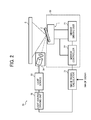
- FIG. 2 there will be described the structures of an optical polarization device 20 for driving the optical polarization mirror 1 illustrated in Fig. 1 , and a two-dimensional image display device 30 including this optical polarization device 20.
- the optical polarization device 20 includes the optical polarization mirror 1 having the mirror 2, a mirror driving unit 21, and a mirror controller 22.
- the mirror controller 22 is implemented by a processor such as a microprocessor, and a memory such as a volatile or nonvolatile memory.
- an image signal calculator 31 determines a laser light-emission intensity and launching timing based on image signals inputted thereto from the outside and, further, outputs control signals to a light source driving unit 32.
- the light source driving unit 32 controls the light emission from a light source 33, based on these control signals.
- the light source 33 outputs a light beam, which irradiates the mirror 2 in the optical polarization mirror 1 through a beam optical system 34, so that images resulted from scanning by the optical polarization device 20 are projected as two-dimensional images onto a projection surface S.
- the optical polarization device 20 performs two-dimensional raster scanning, as illustrated in Fig. 3A , in order to project an appropriate image based on the image signals inputted from the outside, onto the projection surface S.
- the horizontal scanning in the direction of the horizontal axis X corresponds to mechanical resonance driving of the optical polarization mirror 1
- the vertical scanning in the direction of the Y axis corresponds to non-resonance driving of the optical polarization mirror 1.
- the patterns of the voltage waveforms applied to the meander-shaped beam portions 4 in the optical polarization mirror 1 are divided into the voltage signals applied to the longitudinal beam portions 4a and the voltage signals applied to the longitudinal beam portions 4b, as in Fig. 4A .
- the patterns of the voltage waveforms have sawtooth waveforms, and a single period for the vertical scanning direction is divided into an interval within which the applied voltage is gradually changed for raster scanning, and an interval within which the applied voltage is abruptly changed for restoration.
- the time period Ta of a single period is divided into a time period Ta for raster scanning, and a time period Ta2 for restoration.
- the time period of a single period can be expressed as 1/fv, as illustrated in Fig. 4B .
- this adjustment which is referred to as individual adjustment of the driving frequency, is performed by the mirror driving unit 21 under control of the mirror controller 22.
- phase difference ⁇ p between the signals to the longitudinal beam portions 4a and the longitudinal beam portions 4b there are listed the phase difference ⁇ p between the signals to the longitudinal beam portions 4a and the longitudinal beam portions 4b, and the maximum voltage values Va and Vb of the respective signals to the longitudinal beam portions 4a and the longitudinal beam portions 4b.
- the mirror controller 22 stores a value for most improving the light scanning in the vertical direction in its memory and controls the driving of the mirror driving unit 21.
- this adjustment is effective in the uniformity of light scanning, since the configuration of the meander-shaped beam portions 4 having the meander shape is not completely symmetric, in cases of driving in the vertical direction with the configuration of the optical polarization mirror 1.
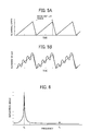
- Fig. 5A illustrates a state where the light scanning speed within the image display range is ideally uniform
- Fig. 5B illustrates a state where speed waving has occurred in a case where a mechanical resonance component interferes with non-resonance driving.
- the period of this waving is 1/f0, with respect to the mechanical resonance frequency f0 in the vertical direction of the optical polarization mirror 1.
- the relative relationship fv/f0 between the resonance frequency and the non-resonance driving is closer to an integer multiple, waving is more prone to be induced.
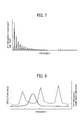
- the specific frequency characteristics in mechanical resonance modes in the vertical direction are as illustrated in Fig. 6 and have two or more resonance frequencies f1, in addition to the resonance frequency f0.
- a voltage signal having a sawtooth waveform illustrated in Figs. 4A to 4D also have a frequency component corresponding to the driving frequency fv.
- n is an integer, as illustrated in Fig. 11 .
- ⁇ T which is a range of temperatures in which the two-dimensional image display device 30 and the optical polarization device 20 will be used
- a driving frequency for maintaining the relationship between the mechanical resonance and the driving frequency which satisfies the Equation 2 is stored in the memory of the mirror controller 22, and the mirror driving unit 21 is controlled therewith.
- the movable frame 3b is rotated in the Y-axis direction and, along therewith, the mirror 2 is also rotated in the vertical direction.
- voltages with a sawtooth waveform are applied to every other piezoelectric member, out of the piezoelectric members 5a and 5b provided independently of the respective beam portions which are meandered, in the longitudinal beam portions 4a and the longitudinal beam portions 4b.
- the voltage application pattern is such that the sawtooth waves to the longitudinal beam portions 4a and the longitudinal beam portions 4b are deviated in phase from each other, for adjusting their maximum voltage values.
- the raster scanning through such non-resonance driving is operated in such a way as to provide rotations of about ⁇ 4 degrees, with sawtooth waves with a frequency of about 60 Hz.
- the waving in the actual images was as illustrated in Fig. 11 .
- the light scanning speed is made constant, which enables providing two-dimensional images having image quality with excellent temperature stability.
- the present invention can be applied to a head-up display device for a vehicle or the like, which employs a diffusion plate as a screen and forms virtual images using a semi-transparent plate or the like. Further, there has been described a structure capable of two-axis scanning as the optical polarization mirror 1, but the present invention can be also applied to an optical polarization device for one-dimensional light scanning through only non-resonance raster scanning.
- the present invention is not limited to only the structure according to the aforementioned embodiment, such that the present invention may be implemented in various other ways to have other designs.
- optical polarization mirror As described above, with the optical polarization mirror according to the embodiment of the present invention, it is possible to ensure a uniform light scanning speed regardless of the ambient environmental temperature during light scanning through non-resonance driving, thereby providing images with higher quality and with reduced brightness unevenness and reduced image distortions, without involving additional sensor mechanisms or complicated signal processing.
Landscapes
- Physics & Mathematics (AREA)
- General Physics & Mathematics (AREA)
- Optics & Photonics (AREA)
- Mechanical Optical Scanning Systems (AREA)
- Transforming Electric Information Into Light Information (AREA)
Abstract
Description
- The present invention relates to optical polarization mirrors, and optical polarization devices and image display devices each employing the optical polarization mirrors.
- In recent years, to achieve size reduction and cost reduction of optical polarization devices and image display devices each provided with optical polarization mirrors, the optical polarization mirrors are fabricated through micro machining to which semiconductor fabrication technique is applied.
- The optical polarization mirror, which polarizes and scans a light beam, is fabricated as a micro electro mechanical systems (MEMS) device through fine processing silicon or glasses, for example, by integrally forming a movable portion provided with a reflective surface and elastic beam-shaped members on a substrate.
- Further, piezoelectric actuator systems may be used as mirror driving systems for such optical polarization mirrors, which are provided with thin-film piezoelectric materials laminated on the elastic beam-shaped members.
- Due to its piezoelectric characteristics, the piezoelectric actuator systems transmit expansions and contractions of the piezoelectric materials to a supporting member forming a cantilever, thus oscillating the cantilever to rotate the mirror.
- Further, on the same plane orthogonal to the optical axis of the light beam, this mirror is rotated about two axes as center axes, which are a first axis (in a horizontal direction) and a second axis (in a vertical direction) orthogonal to each other, thereby enabling two-dimensional scanning.
- On the other hand, in performing two-dimensional light scanning with the optical polarization device using the optical polarization mirror, in general, resonance driving with mechanical resonance frequencies is used for light scanning in the horizontal direction, while non-resonance driving is used for light scanning in the vertical direction.
- For example, for the resonance driving in the horizontal scanning, the cantilever is secured at its one end to a frame portion to be supported thereby, while the cantilever is oscillated at its other end through piezoelectric driving. The oscillations of the cantilever generate torques, which are transmitted to a torsion bar (elastic beam-shaped member) which is coupled to the other end of the cantilever, thereby rotating and driving the mirror installed at the tip end of the torsion bar. This provides a larger scanning angle through driving at lower voltages.
- On the other hand, the non-resonance driving in the vertical direction is used, since there is a need for raster scanning, in order to attain higher fineness and in-surface uniformization, in cases where it is applied to an image display device and the like, for example.
- In general, sawtooth waves are used as driving signals, for performing raster scanning. However, oscillation components of resonance, which are determined by the weight of the movable portion, the rigidity of the cantilever and the like, may interfere with higher harmonics for this driving.
- Such interference of oscillation components of resonance during light scanning may cause brightness unevenness, image distortions and the like to degrade the image quality of displayed images. Accordingly, it is necessary to adjust the amplitude and the phase of the applied driving signal for suppressing oscillations caused by resonance.
- However, if environmental changes including a change in ambient temperature around the optical polarization device are induced, this also changes resonance characteristics in the sub-scanning direction, along with the changes of the piezoelectric characteristics and the physical values of the optical polarization mirror configuration. As a result, the driving signal having been adjusted in such a way as to suppress the interference in the light scanning with respect to the room temperature may be made inappropriate.
- This appears as time-varying brightness unevenness and image distortions in the displayed images during raster scanning, which causes degradations and instability in image quality depending on the environmental temperature.
- In view of this, there have been suggested techniques for ensuring uniformity of the scanning speed during raster scanning (refer to
JP-2011-107505-A - In general, in cases of light scanning in two axes, during light scanning in the vertical direction, a waving phenomenon occurs due to interference between higher harmonics for non-resonance driving and a resonance frequency caused by the configuration for scanning in the vertical direction. This makes the scanning non-uniform.
- According to
JP-2011-107505-A - However, this structure necessitates an additional sensor mechanism for detecting light-scanning speed signals, which complicates the entire device structure and, also, induces the problem of obstruction of the size reduction in the entire device.
- Further, due to light scanning in the two axes, it is impossible to avoid mixture of signals in the horizontal direction and in the vertical direction, which causes the problem of burdens imposed on processing for avoiding the mixture of signals and, further, causes the problem of significant difficulty of completely eliminating such mixture.
- Further, in cases of further coping with the change of the environmental temperature, it is necessary to consider the temperature dependency of the entire device including the sensor mechanism and, also, it is necessary to optimize the respective mechanisms and conditions for performing feedback control, which increases the cost for fabrication such as development cost.
- One of the objectives of at least one embodiment of the present invention is to overcome the aforementioned conventional problems in controlling driving signals for light scanning in the vertical direction for axial raster scanning, thus reducing the non-uniformity of the scanning speed. Further, for an optical polarization device and an image display device using the same optical polarization device, the present invention aims at providing an optical polarization device capable of ensuring scanning uniformity regardless of the ambient environmental temperature with a simple structure. This suppresses the occurrence of brightness unevenness and image distortions for providing images with higher quality.
- Example embodiments of the present invention include an optical polarization device, which includes a mirror (2) having a reflective surface; a pair of meander-shaped beam portions (4) to rotatably support the mirror (2), each meander-shaped beam portion (4) having a plurality of beam portions (4a, 4b) alternately connected at folding-back sections to form a meander shape; a plurality of piezoelectric members (5a, 5b) provided on the respective beam portions (4a, 4b) and applied with voltage waveforms to deform the respective beam portions (4a, 4b), accumulated deformation of the respective beam portions (4a, 4b) causing mirror (2) to rotate; and a voltage controller (22) to individually adjust a driving frequency of each of the voltage waveforms applied to the respective piezoelectric members (5a, 5b).
- Example embodiments of the present invention include image display devices provided with the optical polarization device.
- Example embodiments of the present invention include optical polarization mirrors, which includes: a mirror (2) having a reflective surface; a pair of meander-shaped beam portions (4) to rotatably support the mirror (2), each meander-shaped beam portion (4) having a plurality of beam portions (4a, 4b) alternately connected at folding-back sections to form a meander shape; a plurality of piezoelectric members (5a, 5b) provided on the respective beam portions (4a, 4b) and applied with voltage waveforms to deform the respective beam portions (4a, 4b), accumulated deformation of the respective beam portions (4a, 4b) causing mirror (2) to rotate, in which a driving frequency of each of the voltage waveforms applied to the respective piezoelectric members (5a, 5b) is individually adjusted.
- With this configuration, scanning uniformity is ensured regardless of the ambient environmental temperature, with a simple structure. This further suppresses the occurrence of brightness unevenness and image distortions for providing images with higher quality.
- A more complete appreciation of the disclosure and many of the attendant advantages and features thereof can be readily obtained and understood from the following detailed description with reference to the accompanying drawings, wherein:
-
Fig. 1 is a front view of an optical polarization mirror which is applied to an optical polarization device according to an embodiment of the present invention; -
Fig. 2 is a block diagram illustrating a structure a two-dimensional image display device using the optical polarization device according to an embodiment of the present invention; -
Figs. 3A and 3B illustrate the optical polarization device according to the embodiment of the present invention,Fig. 3A is an explanation view of raster scanning, andFig. 3B is a graphic view of reciprocating scanning deviations induced during raster scanning; -
Figs. 4A to 4D are graphic views of examples of driving signals for the optical polarization mirror in the optical polarization device according to the embodiment of the present invention; -
Figs. 5A and 5B illustrate the optical polarization device according to the embodiment of the present invention,Fig. 5A is a graphic view of ideal raster scanning, andFig. 5B is a graphic view of a state where speed waving has occurred in a case where a mechanical resonance component interferes with non-resonance driving; -
Fig. 6 is a graphic view of a specific frequency characteristic in mechanical resonance modes in the vertical direction of the optical polarization mirror in the optical polarization device according to the embodiment of the present invention; -
Fig. 7 is a graphic view of frequency components resulted from an FFT analysis performed on frequency components of a mirror driving signal; -
Fig. 8 is a graphic diagram illustrating overlapping between mechanical resonance and frequency components of driving signals; -
Fig. 9 is a graphic diagram of a resonance frequency characteristic of a linear temperature coefficient; -
Fig. 10 is a graphic diagram illustrating the relative relationship between the resonance frequency and the driving frequency of the optical polarization mirror; -
Fig. 11 is a graphic view for illustrating (temperature) the temperature dependency of image light-intensity unevenness in two-dimensional image display using the optical polarization device according to the embodiment of the present invention; and -
Fig. 12 is a graphic view for illustrating (vertical axis Y) the temperature dependency of the image light-intensity unevenness in two-dimensional image display using the optical polarization device according to the embodiment of the present invention. - The accompanying drawings are intended to depict example embodiments of the present invention and should not be interpreted to limit the scope thereof. The accompanying drawings are not to be considered as drawn to scale unless explicitly noted.
- The terminology used herein is for the purpose of describing particular embodiments only and is not intended to be limiting of the present invention. As used herein, the singular forms "a", "an" and "the" are intended to include the plural forms as well, unless the context clearly indicates otherwise. It will be further understood that the terms "includes" and/or "including", when used in this specification, specify the presence of stated features, integers, steps, operations, elements, and/or components, but do not preclude the presence or addition of one or more other features, integers, steps, operations, elements, components, and/or groups thereof.
- In describing example embodiments shown in the drawings, specific terminology is employed for the sake of clarity. However, the present disclosure is not intended to be limited to the specific terminology so selected and it is to be understood that each specific element includes all technical equivalents that operate in a similar manner.
- Hereinafter, there will be described an optical polarization mirror according to an embodiment of the present invention.
- The optical polarization mirror in an optical polarization device for performing light scanning through non-resonance driving according to this embodiment of the present invention is structured to have cantilevers provided with piezoelectric materials in a mender shape. Out of these cantilevers, different voltages are applied to every other cantilevers for causing warpage in the respective cantilevers, thus rotating a reflective surface for light scanning.
- In this case, the voltages applied to every other cantilevers are sawtooth waves having such a pattern that a rising time period and a falling time period in a single period are alternately interchanged. Their relative phases and their maximum voltage values are adjusted, thereby reducing the waving of the scanning speed due to mechanical resonance.
- However, in cases where physical constants of the members are changed along with the ambient environmental temperature, and the resonance frequency derived from the configuration is changed, oscillations of mechanical resonance may be enhanced by the non-resonance driving, which may change the uniformity of the light scanning speed in the vertical direction. This has induced variations and degradations in image qualities, in some cases.
- In view of this, in the present invention, for an assumed environmental temperature range for the optical polarization mirror, the optical polarization device and the image projection device, and for variations of the resonance frequency of the optical polarization mirror at that time, the relative value of the frequency of the driving signal applied to every other cantilever with respect to the resonance frequency is continuously deviated from an integer-multiple relationship. This improves the uniformity of the light scanning speed of the mirror, thereby realizing sufficient linearity regardless of the temperature.
- Meander-shaped cantilevers are coupled and connected to the optical polarization mirror for use in the present invention. This device structure is designed in such a way as to ensure symmetry for safe operations, but it is impossible to make it have a completely symmetric shape due to characteristics of the meander-shaped pattern.
- In this case, if there is such an integer-multiple relative relationship between the resonance frequency and the driving frequency, oscillation components caused by resonance are enhanced by operation components of the reflection mirror, and the resonance interferes with the higher harmonics for light scanning, which induces a waving phenomenon, thereby degrading the scanning uniformity.
- Therefore, for assumed temperature variations and for the range within which the resonance frequency varies, the driving signal is adjusted such that the relative value of the frequency of the applied driving signal with respect to the resonance frequency is continuously deviated from an integer-multiple relationship. This suppresses the interference of oscillations caused by mechanical resonance with the light scanning through the non-resonance driving.
- With the mechanism for adjusting the driving signal, it is possible to form images with higher quality and with excellent speed uniformity.
- With the adjusted driving signal, images can be uniform over a wider temperature range such that it is not necessary to have a detection device such as a new temperature sensor.
- Further, it is possible to provide uniform images, in a state where there is no need for performing complicated signal processing.
- Hereinafter, the optical polarization device according to the present invention will be described in detail, with reference to the drawings. At first, with reference to
Fig. 1 , there will be described the structure of a polarization mirror adapted to polarize and scan a light beam according to the embodiment of the present invention. - An
optical polarization mirror 1 has respective members which have been formed integrally through an MEMS process, which will be described later. Further, theoptical polarization mirror 1 includes a frame member 3 in which there is placed, at an approximate center thereof, amirror 2 with a laser-lightreflective surface 2a over its surface. - The
mirror 2 is rotatable about two axes as center axes (a horizontal axis X and a vertical axis Y), which are orthogonal to each other in the same plane orthogonal to an optical axis P of laser light, to display two-dimensional images. - The frame member 3 supports a pair of meander-shaped
beam portions 4 which are supported by anouter frame 3a at their respective one ends and are supported by amovable frame 3b at their respective other ends. - The pair of the meander-shaped
beam portions 4 each includeslongitudinal beam portions beam portions lateral beam portions 4c extending shortly along the horizontal axis X, which serve as folding-back sections. With this configuration, the pair of the meander-shapedbeam portions 4 are formed to meander. Thus, the meander-shapedbeam portions 4 are alternately divided into thelongitudinal beam portions 4a and thelongitudinal beam portions 4b, at their portions along the vertical axis Y except thelateral beam portions 4c. These respectivelongitudinal beam portions - The
movable frame 3b has a pair oftorsion bars mirror 2, and drivingbeams - Light scanning in the vertical direction of the
mirror 2 about the horizontal axis X is performed as follows. The respectivepiezoelectric members beam portions 4 for deflecting thelongitudinal beam portions mirror 2 about the horizontal axis X in a non-resonance manner, thereby causing theoptical polarization mirror 1 to play the function of a piezoelectric-type optical polarization mirror. - On the other hand, scanning in the horizontal direction of the
mirror 2 about the vertical axis Y is performed through resonance driving using the drivingbeams torsion bars mirror 2. - With this structure, it is possible to perform light scanning, at the same time, in the directions of the two axes which are the horizontal axis X and the vertical axis Y.
- Next, with reference to
Fig. 2 , there will be described the structures of anoptical polarization device 20 for driving theoptical polarization mirror 1 illustrated inFig. 1 , and a two-dimensionalimage display device 30 including thisoptical polarization device 20. - The
optical polarization device 20 includes theoptical polarization mirror 1 having themirror 2, amirror driving unit 21, and amirror controller 22. - In this embodiment, the
mirror controller 22 is implemented by a processor such as a microprocessor, and a memory such as a volatile or nonvolatile memory. - In the two-dimensional
image display device 30, animage signal calculator 31 determines a laser light-emission intensity and launching timing based on image signals inputted thereto from the outside and, further, outputs control signals to a lightsource driving unit 32. The lightsource driving unit 32 controls the light emission from a light source 33, based on these control signals. The light source 33 outputs a light beam, which irradiates themirror 2 in theoptical polarization mirror 1 through a beamoptical system 34, so that images resulted from scanning by theoptical polarization device 20 are projected as two-dimensional images onto a projection surface S. - In this case, the
optical polarization device 20 performs two-dimensional raster scanning, as illustrated inFig. 3A , in order to project an appropriate image based on the image signals inputted from the outside, onto the projection surface S. Further, inFig. 3A , the horizontal scanning in the direction of the horizontal axis X corresponds to mechanical resonance driving of theoptical polarization mirror 1, while the vertical scanning in the direction of the Y axis corresponds to non-resonance driving of theoptical polarization mirror 1. - In this case, in the vertical scanning direction, similarly, due to the weights, rigidities and the like of the respective members including the
optical polarization mirror 1, and the like, there exists a specific resonance frequency, which may interfere with the oscillations of the non-resonance driving. This may cause an appearance of light intensity waving in the Y-axis direction, namely image intensity unevenness, as illustrated inFig. 3B . - Hereinafter, with reference to
Figs. 4A to 4D , a non-resonance driving method for theoptical polarization mirror 1 will be described. In the following description, it will be assumed that voltage waveforms are applied to thelongitudinal beam portions 4a and thelongitudinal beam portions 4b, for convenience of description, although they are applied to thepiezoelectric members - The patterns of the voltage waveforms applied to the meander-shaped
beam portions 4 in theoptical polarization mirror 1 are divided into the voltage signals applied to thelongitudinal beam portions 4a and the voltage signals applied to thelongitudinal beam portions 4b, as inFig. 4A . - The patterns of the voltage waveforms have sawtooth waveforms, and a single period for the vertical scanning direction is divided into an interval within which the applied voltage is gradually changed for raster scanning, and an interval within which the applied voltage is abruptly changed for restoration.
- More specifically, regarding the voltage applied to the
longitudinal beam portions 4a, the time period Ta of a single period is divided into a time period Ta for raster scanning, and a time period Ta2 for restoration. In this case, assuming that the ratio of the time period for raster scanning to the time period of a single period is a symmetry Sa, there is held Sa=Ta1/Ta. - Similarly, regarding the voltage applied to the
longitudinal beam portions 4b, with respect to the time period Tb of a single period, there is held Sb=Tb1/Tb. Further, with the driving frequency fv of the applied-voltage signal having the waveform, the time period of a single period can be expressed as 1/fv, as illustrated inFig. 4B . Further, this adjustment, which is referred to as individual adjustment of the driving frequency, is performed by themirror driving unit 21 under control of themirror controller 22. - On the other hand, in order to suppress the image unevenness illustrated in
Fig. 3B , it is necessary to determine the uniformity of the light scanning speed in the vertical direction, and it is necessary to set signals for most improving the uniformity. - As setting parameters, as illustrated in
Fig. 4D , there are listed the phase difference Δp between the signals to thelongitudinal beam portions 4a and thelongitudinal beam portions 4b, and the maximum voltage values Va and Vb of the respective signals to thelongitudinal beam portions 4a and thelongitudinal beam portions 4b. - The
mirror controller 22 stores a value for most improving the light scanning in the vertical direction in its memory and controls the driving of themirror driving unit 21. - In this case, this adjustment is effective in the uniformity of light scanning, since the configuration of the meander-shaped
beam portions 4 having the meander shape is not completely symmetric, in cases of driving in the vertical direction with the configuration of theoptical polarization mirror 1. - Therefore, by compensating for the slight asymmetry through the adjustment of the values of the voltages to the
longitudinal beam portions 4a and thelongitudinal beam portions 4b, it is possible to suppress the induction of mechanical resonance. - However, with only this method, it is impossible to sufficiently suppress the variation of the light scanning speed along with the variation of the mechanical resonance frequency, which follows the change in ambient temperature around the
optical polarization mirror 1. -
Fig. 5A illustrates a state where the light scanning speed within the image display range is ideally uniform, andFig. 5B illustrates a state where speed waving has occurred in a case where a mechanical resonance component interferes with non-resonance driving. - The period of this waving is 1/f0, with respect to the mechanical resonance frequency f0 in the vertical direction of the
optical polarization mirror 1. - Namely, as the relative relationship fv/f0 between the resonance frequency and the non-resonance driving is closer to an integer multiple, waving is more prone to be induced. In this case, the specific frequency characteristics in mechanical resonance modes in the vertical direction are as illustrated in
Fig. 6 and have two or more resonance frequencies f1, in addition to the resonance frequency f0. - As a result thereof, a voltage signal having a sawtooth waveform illustrated in
Figs. 4A to 4D also have a frequency component corresponding to the driving frequency fv. By performing an FFT analysis thereon, it is possible to recognize frequency components as illustrated inFig. 7 . - Therefore, as illustrated in
Fig. 8 , there is a need for taking account of the overlap between the mechanical resonance and the frequency components of the driving signal. In this case, the specific frequencies in mechanical resonance modes as illustrated inFig. 6 have temperature dependency, due to the changes of the physical properties of the members and the performance of the thin-film materials in thepiezoelectric members - For addressing this, the
optical polarization mirror 1 has a resonance frequency characteristic having a linear temperature coefficient as illustrated inFig. 9 , and this temperature gradient is assumed to be "a". Further, assuming that the temperature change around theoptical polarization mirror 1 is ΔT, and the shift of the resonance frequency is Δf, it is possible to express the relationship therebetween, as follows.
- Further, for addressing the ambient temperature change, in order to maintain the uniformity of the light scanning speed of the
optical polarization mirror 1, it is necessary to satisfy the following relationship, assuming that "n" is an integer, as illustrated inFig. 11 .
- Namely, adjustments are performed as follows. Based on the used temperature range ΔT which is a range of temperatures in which the two-dimensional
image display device 30 and theoptical polarization device 20 will be used, a driving frequency for maintaining the relationship between the mechanical resonance and the driving frequency which satisfies theEquation 2 is stored in the memory of themirror controller 22, and themirror driving unit 21 is controlled therewith. - This enables continuously maintaining a linear light scanning speed uniformity over a wider temperature range, at the same set driving frequency, as illustrated in
Fig. 12 , without performing complicated adjustment every time the temperature has changed. Further, as illustrated inFig. 12 , it is possible to eliminate brightness unevenness and image pattern distortions, which are prone to be induced in images in the vertical direction. Further, it is possible to project images with higher quality regardless of the environment, without performing complicated signal processing such as driving control based on temperature table data, using external temperature detection means, and the like. - This enables alleviating the problems of image amplitude deviations, deviations between mirror scanning timing and light-emission synchronization timing, and image fluctuations, due to waving of the light scanning speed, in the two-dimensional
image display device 30. - Further, by combining the mechanism for adjusting the driving frequency with the mechanism for adjusting the values of the voltages to the respective meander-shaped
beam portions 4, it is possible to perform light scanning with higher quality and lower temperature dependency. - Further, even when slight unevenness is induced due to working errors generated in the fabrication processing for the optical polarization device and the positions of the piezoelectric members, it is possible to compensate for these errors through the mechanism for adjusting the driving frequency. Therefore, it is possible to improve the uniformity in the sub-scanning direction and, concurrently, it is possible to compensate for errors resulted from working, thereby increasing the yield in the fabrication processing.
- Hereinafter, there will be described an example of control of the
optical polarization mirror 1 by themirror controller 22 according to the present invention. More specifically, for horizontal scanning in the X direction along the horizontal axis, a sinusoidal voltage with a frequency of about 20 kHz, which is a higher frequency by several tens of Hz than the resonance frequency, is applied, so that themirror 2 is rotated at about 20 kHz through torsions of thetorsion bars mirror 2, theoptical polarization mirror 1 is operated such that themirror 2 can rotate by about ±10 degrees. - On the other hand, by driving the
longitudinal beam portions 4a and thelongitudinal beam portions 4b, themovable frame 3b is rotated in the Y-axis direction and, along therewith, themirror 2 is also rotated in the vertical direction. - More specifically, voltages with a sawtooth waveform are applied to every other piezoelectric member, out of the
piezoelectric members longitudinal beam portions 4a and thelongitudinal beam portions 4b. The voltage application pattern is such that the sawtooth waves to thelongitudinal beam portions 4a and thelongitudinal beam portions 4b are deviated in phase from each other, for adjusting their maximum voltage values. In this case, the adjustment is set in such a way as to satisfy the relationship of f0/fv=n, n+1/2. The raster scanning through such non-resonance driving is operated in such a way as to provide rotations of about ±4 degrees, with sawtooth waves with a frequency of about 60 Hz. - Two-dimensional images were displayed, using two-axis scanning with the
optical polarization mirror 1. Further, the driving conditions were set to satisfy the relationships of f0/fv=n and f0/fv=n+1/2, and image light-intensity unevenness was determined within the temperature range of about -25 degrees C to 75 degrees C, for the respective driving conditions. - As a result thereof, as illustrated in
Fig. 10 , under the condition where the relative relationship between the resonance and the driving frequency was "n" times, more image quality degradations were observed as the temperature was deviated from the room temperature. With light scanning satisfying the relationship ofEquation 2, the image quality degradation due to the temperature was reduced to about 1/10 or less. - The waving in the actual images was as illustrated in
Fig. 11 . With the lightscanning satisfying Equation 2, the light scanning speed is made constant, which enables providing two-dimensional images having image quality with excellent temperature stability. - There has been illustrated an example where one or more light sources 33 are mainly used, and laser light having been subjected to two-dimensional light scanning through the
optical polarization mirror 1 is projected onto the projection surface S such as a screen, as described above, but the present invention is not limited thereto. - For example, the present invention can be applied to a head-up display device for a vehicle or the like, which employs a diffusion plate as a screen and forms virtual images using a semi-transparent plate or the like. Further, there has been described a structure capable of two-axis scanning as the
optical polarization mirror 1, but the present invention can be also applied to an optical polarization device for one-dimensional light scanning through only non-resonance raster scanning. - As described above, the present invention is not limited to only the structure according to the aforementioned embodiment, such that the present invention may be implemented in various other ways to have other designs.
- As described above, with the optical polarization mirror according to the embodiment of the present invention, it is possible to ensure a uniform light scanning speed regardless of the ambient environmental temperature during light scanning through non-resonance driving, thereby providing images with higher quality and with reduced brightness unevenness and reduced image distortions, without involving additional sensor mechanisms or complicated signal processing.
- Numerous additional modifications and variations are possible in light of the above teachings. It is therefore to be understood that within the scope of the appended claims, the disclosure of the present invention may be practiced otherwise than as specifically described herein. For example, elements and/or features of different illustrative embodiments may be combined with each other and/or substituted for each other within the scope of this disclosure and appended claims.
Claims (9)
- An optical polarization device (20) comprising:a mirror (2) having a reflective surface;a pair of meander-shaped beam portions (4) configured to rotatably support the mirror (2), each meander-shaped beam portion (4) having a plurality of beam portions (4a, 4b) alternately connected at folding-back sections to form a meander shape;a plurality of piezoelectric members (5a, 5b) provided on the respective beam portions (4a, 4b) and applied with voltage waveforms to deform the respective beam portions (4a, 4b), wherein accumulated deformation of the respective beam portions (4a, 4b) causes mirror (2) to rotate; anda voltage controller (22) configured to individually adjust a driving frequency of each of the voltage waveforms applied to the respective piezoelectric members (5a, 5b).
- The optical polarization device (2) according to Claim 1, wherein
the voltage controller (22) is configured to apply two different types of voltage waveforms to every other beam portions (4a, 4b) through corresponding ones of the plurality of piezoelectric members (5a, 5b), and to adjust the driving frequencies of the two types of the applied voltage waveforms. - The optical polarization device (2) according to Claim 2, wherein
the voltage controller (22) is configured to store the respective driving frequencies (fv) of the two types of the applied voltage waveforms in a memory, and to apply the voltage waveforms to the respective piezoelectric members (5a, 5b) based on the stored values of the respective driving frequencies (fv). - The optical polarization device (2) according to Claim 3, wherein
the voltage controller (22) is configured to store a resonance frequency (f0) of the optical polarization device (2) in addition to the respective driving frequencies (fv) of the two types of the voltage waveforms, and to apply a voltage to each of the piezoelectric members (5a, 5b), based on a relative value of each of the driving frequencies (fv) of the two types of the voltage waveforms with respect to the resonance frequency (f0). - The optical polarization device (2) according to Claim 4, wherein
the voltage controller (22) is configured to apply the voltage to each of the piezoelectric members (5a, 5b), so as to satisfy a driving condition which prevents the ratio between the resonance frequency (f0) and each of the driving frequencies (fv) from being an integer multiple. - The optical polarization device (2) according to Claim 5, wherein
the voltage controller (22) is configured to individually adjust a maximum value of the voltage waveform applied to each of the piezoelectric members (5a, 5b) and to adjust the value of the driving frequency (fv). - An image projection device comprising the optical polarization device (2) according to any one of Claims 1 to 6.
- An optical polarization mirror (1) comprising:a mirror (2) having a reflective surface;a pair of meander-shaped beam portions (4) configured to rotatably support the mirror (2), each meander-shaped beam portion (4) having a plurality of beam portions (4a, 4b) alternately connected at folding-back sections to form a meander shape; anda plurality of piezoelectric members (5a, 5b) provided on the respective beam portions (4a, 4b) and applied with voltage waveforms to deform the respective beam portions (4a, 4b), wherein accumulated deformation of the respective beam portions (4a, 4b) causes mirror (2) to rotate,wherein each of the voltage waveforms applied to the respective piezoelectric members (5a, 5b) is individually adjusted.
- The optical polarization mirror (1) according to Claim 8, wherein
the mirror (2) is configured to perform two-dimensional light scanning while rotating about two axes orthogonal to each other within the same plane orthogonal to an optical axis, and
each of the voltage waveforms is applied to the respective piezoelectric members (5a, 5b) to cause the mirror (2) to rotate about at least one axis of the two axes.
Applications Claiming Priority (1)
| Application Number | Priority Date | Filing Date | Title |
|---|---|---|---|
| JP2014050337A JP6533365B2 (en) | 2014-03-13 | 2014-03-13 | Light deflection device, light deflection mirror and image display device |
Publications (2)
| Publication Number | Publication Date |
|---|---|
| EP2924485A1 true EP2924485A1 (en) | 2015-09-30 |
| EP2924485B1 EP2924485B1 (en) | 2023-03-01 |
Family
ID=52810941
Family Applications (1)
| Application Number | Title | Priority Date | Filing Date |
|---|---|---|---|
| EP15158672.4A Active EP2924485B1 (en) | 2014-03-13 | 2015-03-11 | Optical deflection device, and image display device |
Country Status (2)
| Country | Link |
|---|---|
| EP (1) | EP2924485B1 (en) |
| JP (1) | JP6533365B2 (en) |
Cited By (3)
| Publication number | Priority date | Publication date | Assignee | Title |
|---|---|---|---|---|
| CN110945404A (en) * | 2017-07-25 | 2020-03-31 | 浜松光子学株式会社 | Scanning device |
| CN112432766A (en) * | 2020-09-23 | 2021-03-02 | 菲兹克光电(长春)有限公司 | Method for detecting performance of laser scanning galvanometer |
| EP4394479A1 (en) * | 2022-12-29 | 2024-07-03 | Silicon Austria Labs GmbH | Micromirror device and method operating same |
Families Citing this family (3)
| Publication number | Priority date | Publication date | Assignee | Title |
|---|---|---|---|---|
| JP2017116842A (en) * | 2015-12-25 | 2017-06-29 | 株式会社リコー | Optical deflector and image projection apparatus |
| JP2019095353A (en) * | 2017-11-24 | 2019-06-20 | パイオニア株式会社 | Ranging device |
| JPWO2023190068A1 (en) * | 2022-03-29 | 2023-10-05 |
Citations (3)
| Publication number | Priority date | Publication date | Assignee | Title |
|---|---|---|---|---|
| JP2011107505A (en) | 2009-11-19 | 2011-06-02 | Konica Minolta Opto Inc | Two-dimensional optical scanner driving device |
| EP2495600A1 (en) * | 2011-03-04 | 2012-09-05 | Stanley Electric Co., Ltd. | Driver for optical deflector using complex-sinusoidal-wave drive voltages and method for setting the same |
| EP2848978A1 (en) * | 2013-09-13 | 2015-03-18 | Ricoh Company Ltd. | Optical deflecting device, apparatus including the same, and method of controlling optical deflecting device |
Family Cites Families (6)
| Publication number | Priority date | Publication date | Assignee | Title |
|---|---|---|---|---|
| US7031040B2 (en) * | 2003-05-16 | 2006-04-18 | Ricoh Company, Ltd. | Optical scanning apparatus, optical writing apparatus, image forming apparatus, and method of driving vibration mirror |
| US8059322B1 (en) * | 2008-09-16 | 2011-11-15 | National Semiconductor Corporation | System for suppressing undesirable oscillations in a MEMS scanner |
| JP5670227B2 (en) * | 2011-03-04 | 2015-02-18 | スタンレー電気株式会社 | Drive device for optical deflector |
| JP5845394B2 (en) * | 2011-05-17 | 2016-01-20 | パナソニックIpマネジメント株式会社 | Optical scanning device |
| JP5652336B2 (en) * | 2011-06-06 | 2015-01-14 | 株式会社Jvcケンウッド | Optical scanning device |
| JP2013205818A (en) * | 2012-03-29 | 2013-10-07 | Stanley Electric Co Ltd | Light deflector |
-
2014
- 2014-03-13 JP JP2014050337A patent/JP6533365B2/en active Active
-
2015
- 2015-03-11 EP EP15158672.4A patent/EP2924485B1/en active Active
Patent Citations (3)
| Publication number | Priority date | Publication date | Assignee | Title |
|---|---|---|---|---|
| JP2011107505A (en) | 2009-11-19 | 2011-06-02 | Konica Minolta Opto Inc | Two-dimensional optical scanner driving device |
| EP2495600A1 (en) * | 2011-03-04 | 2012-09-05 | Stanley Electric Co., Ltd. | Driver for optical deflector using complex-sinusoidal-wave drive voltages and method for setting the same |
| EP2848978A1 (en) * | 2013-09-13 | 2015-03-18 | Ricoh Company Ltd. | Optical deflecting device, apparatus including the same, and method of controlling optical deflecting device |
Cited By (5)
| Publication number | Priority date | Publication date | Assignee | Title |
|---|---|---|---|---|
| CN110945404A (en) * | 2017-07-25 | 2020-03-31 | 浜松光子学株式会社 | Scanning device |
| US11644666B2 (en) | 2017-07-25 | 2023-05-09 | Hamamatsu Photonics K.K. | Scanning device |
| CN112432766A (en) * | 2020-09-23 | 2021-03-02 | 菲兹克光电(长春)有限公司 | Method for detecting performance of laser scanning galvanometer |
| CN112432766B (en) * | 2020-09-23 | 2024-07-12 | 菲兹克光电(长春)有限公司 | Laser scanning galvanometer performance detection method |
| EP4394479A1 (en) * | 2022-12-29 | 2024-07-03 | Silicon Austria Labs GmbH | Micromirror device and method operating same |
Also Published As
| Publication number | Publication date |
|---|---|
| JP2015175889A (en) | 2015-10-05 |
| JP6533365B2 (en) | 2019-06-19 |
| EP2924485B1 (en) | 2023-03-01 |
Similar Documents
| Publication | Publication Date | Title |
|---|---|---|
| EP2924485B1 (en) | Optical deflection device, and image display device | |
| JP6012276B2 (en) | Deflection device for a scanner performing Lissajous scanning | |
| JP5659056B2 (en) | Drive device for optical deflector | |
| EP3814826B1 (en) | Adjusting a resonant frequency of a scanning mirror | |
| US8786926B2 (en) | Driver for optical deflector using two asyncronous saw-tooth drive voltages and method for setting the same | |
| JP5689477B2 (en) | Deflection device for projection device, projection device for projecting image, and method for controlling deflection device for projection device | |
| JP6641709B2 (en) | Optical deflection device, image forming device, image display device, moving body device, and adjustment method for optical deflection device | |
| JP5184909B2 (en) | Oscillator device and optical deflection device | |
| CN109991732B (en) | Scanning reflector device and method for driving a reflector system | |
| US8325407B2 (en) | Oscillating device, optical scanning device using the same, image display apparatus, and control method of the oscillating device | |
| JP2017010005A (en) | Optical deflection device, image formation device, image display device, body device, and method of adjusting optical deflection device | |
| JP5769941B2 (en) | Actuator drive | |
| JP2008310295A (en) | Image display apparatus | |
| US8270057B2 (en) | Oscillator device, optical deflecting device and method of controlling the same | |
| JP6398599B2 (en) | Optical deflection apparatus, optical scanning apparatus, image projection apparatus, and head-up display | |
| EP2891917B1 (en) | Optical deflection device, optical scanning apparatus, image display apparatus, and image forming apparatus | |
| JP7027689B2 (en) | Light deflector and image projection device | |
| JP6789704B2 (en) | Optical scanning device | |
| JP2010048928A (en) | Oscillating body device and light deflector using the same | |
| EP4354199B1 (en) | Mems optical deflector and optical scanning device | |
| US20240288683A1 (en) | Microscanner having meander spring-based mirror suspension | |
| JP5341372B2 (en) | Oscillator device and image forming apparatus using the oscillator device | |
| JP2011123246A (en) | Optical reflecting element | |
| JP6369357B2 (en) | Scanning device | |
| JP5235511B2 (en) | Optical scanning device, driving method thereof, and optical apparatus |
Legal Events
| Date | Code | Title | Description |
|---|---|---|---|
| PUAI | Public reference made under article 153(3) epc to a published international application that has entered the european phase |
Free format text: ORIGINAL CODE: 0009012 |
|
| 17P | Request for examination filed |
Effective date: 20150311 |
|
| AK | Designated contracting states |
Kind code of ref document: A1 Designated state(s): AL AT BE BG CH CY CZ DE DK EE ES FI FR GB GR HR HU IE IS IT LI LT LU LV MC MK MT NL NO PL PT RO RS SE SI SK SM TR |
|
| AX | Request for extension of the european patent |
Extension state: BA ME |
|
| RIN1 | Information on inventor provided before grant (corrected) |
Inventor name: SHINKAWA, MIZUKI Inventor name: HASIGUCHI, TSUYOSHI |
|
| STAA | Information on the status of an ep patent application or granted ep patent |
Free format text: STATUS: EXAMINATION IS IN PROGRESS |
|
| 17Q | First examination report despatched |
Effective date: 20190528 |
|
| GRAP | Despatch of communication of intention to grant a patent |
Free format text: ORIGINAL CODE: EPIDOSNIGR1 |
|
| STAA | Information on the status of an ep patent application or granted ep patent |
Free format text: STATUS: GRANT OF PATENT IS INTENDED |
|
| INTG | Intention to grant announced |
Effective date: 20221020 |
|
| GRAS | Grant fee paid |
Free format text: ORIGINAL CODE: EPIDOSNIGR3 |
|
| GRAA | (expected) grant |
Free format text: ORIGINAL CODE: 0009210 |
|
| STAA | Information on the status of an ep patent application or granted ep patent |
Free format text: STATUS: THE PATENT HAS BEEN GRANTED |
|
| AK | Designated contracting states |
Kind code of ref document: B1 Designated state(s): AL AT BE BG CH CY CZ DE DK EE ES FI FR GB GR HR HU IE IS IT LI LT LU LV MC MK MT NL NO PL PT RO RS SE SI SK SM TR |
|
| REG | Reference to a national code |
Ref country code: GB Ref legal event code: FG4D |
|
| REG | Reference to a national code |
Ref country code: CH Ref legal event code: EP Ref country code: AT Ref legal event code: REF Ref document number: 1551389 Country of ref document: AT Kind code of ref document: T Effective date: 20230315 |
|
| REG | Reference to a national code |
Ref country code: DE Ref legal event code: R096 Ref document number: 602015082625 Country of ref document: DE |
|
| REG | Reference to a national code |
Ref country code: IE Ref legal event code: FG4D |
|
| REG | Reference to a national code |
Ref country code: LT Ref legal event code: MG9D |
|
| REG | Reference to a national code |
Ref country code: NL Ref legal event code: MP Effective date: 20230301 |
|
| PG25 | Lapsed in a contracting state [announced via postgrant information from national office to epo] |
Ref country code: RS Free format text: LAPSE BECAUSE OF FAILURE TO SUBMIT A TRANSLATION OF THE DESCRIPTION OR TO PAY THE FEE WITHIN THE PRESCRIBED TIME-LIMIT Effective date: 20230301 Ref country code: NO Free format text: LAPSE BECAUSE OF FAILURE TO SUBMIT A TRANSLATION OF THE DESCRIPTION OR TO PAY THE FEE WITHIN THE PRESCRIBED TIME-LIMIT Effective date: 20230601 Ref country code: LV Free format text: LAPSE BECAUSE OF FAILURE TO SUBMIT A TRANSLATION OF THE DESCRIPTION OR TO PAY THE FEE WITHIN THE PRESCRIBED TIME-LIMIT Effective date: 20230301 Ref country code: LT Free format text: LAPSE BECAUSE OF FAILURE TO SUBMIT A TRANSLATION OF THE DESCRIPTION OR TO PAY THE FEE WITHIN THE PRESCRIBED TIME-LIMIT Effective date: 20230301 Ref country code: HR Free format text: LAPSE BECAUSE OF FAILURE TO SUBMIT A TRANSLATION OF THE DESCRIPTION OR TO PAY THE FEE WITHIN THE PRESCRIBED TIME-LIMIT Effective date: 20230301 Ref country code: ES Free format text: LAPSE BECAUSE OF FAILURE TO SUBMIT A TRANSLATION OF THE DESCRIPTION OR TO PAY THE FEE WITHIN THE PRESCRIBED TIME-LIMIT Effective date: 20230301 |
|
| REG | Reference to a national code |
Ref country code: AT Ref legal event code: MK05 Ref document number: 1551389 Country of ref document: AT Kind code of ref document: T Effective date: 20230301 |
|
| P01 | Opt-out of the competence of the unified patent court (upc) registered |
Effective date: 20230714 |
|
| PG25 | Lapsed in a contracting state [announced via postgrant information from national office to epo] |
Ref country code: SE Free format text: LAPSE BECAUSE OF FAILURE TO SUBMIT A TRANSLATION OF THE DESCRIPTION OR TO PAY THE FEE WITHIN THE PRESCRIBED TIME-LIMIT Effective date: 20230301 Ref country code: PL Free format text: LAPSE BECAUSE OF FAILURE TO SUBMIT A TRANSLATION OF THE DESCRIPTION OR TO PAY THE FEE WITHIN THE PRESCRIBED TIME-LIMIT Effective date: 20230301 Ref country code: NL Free format text: LAPSE BECAUSE OF FAILURE TO SUBMIT A TRANSLATION OF THE DESCRIPTION OR TO PAY THE FEE WITHIN THE PRESCRIBED TIME-LIMIT Effective date: 20230301 Ref country code: GR Free format text: LAPSE BECAUSE OF FAILURE TO SUBMIT A TRANSLATION OF THE DESCRIPTION OR TO PAY THE FEE WITHIN THE PRESCRIBED TIME-LIMIT Effective date: 20230602 Ref country code: FI Free format text: LAPSE BECAUSE OF FAILURE TO SUBMIT A TRANSLATION OF THE DESCRIPTION OR TO PAY THE FEE WITHIN THE PRESCRIBED TIME-LIMIT Effective date: 20230301 |
|
| PG25 | Lapsed in a contracting state [announced via postgrant information from national office to epo] |
Ref country code: SM Free format text: LAPSE BECAUSE OF FAILURE TO SUBMIT A TRANSLATION OF THE DESCRIPTION OR TO PAY THE FEE WITHIN THE PRESCRIBED TIME-LIMIT Effective date: 20230301 Ref country code: RO Free format text: LAPSE BECAUSE OF FAILURE TO SUBMIT A TRANSLATION OF THE DESCRIPTION OR TO PAY THE FEE WITHIN THE PRESCRIBED TIME-LIMIT Effective date: 20230301 Ref country code: PT Free format text: LAPSE BECAUSE OF FAILURE TO SUBMIT A TRANSLATION OF THE DESCRIPTION OR TO PAY THE FEE WITHIN THE PRESCRIBED TIME-LIMIT Effective date: 20230703 Ref country code: EE Free format text: LAPSE BECAUSE OF FAILURE TO SUBMIT A TRANSLATION OF THE DESCRIPTION OR TO PAY THE FEE WITHIN THE PRESCRIBED TIME-LIMIT Effective date: 20230301 Ref country code: CZ Free format text: LAPSE BECAUSE OF FAILURE TO SUBMIT A TRANSLATION OF THE DESCRIPTION OR TO PAY THE FEE WITHIN THE PRESCRIBED TIME-LIMIT Effective date: 20230301 Ref country code: AT Free format text: LAPSE BECAUSE OF FAILURE TO SUBMIT A TRANSLATION OF THE DESCRIPTION OR TO PAY THE FEE WITHIN THE PRESCRIBED TIME-LIMIT Effective date: 20230301 |
|
| REG | Reference to a national code |
Ref country code: CH Ref legal event code: PL |
|
| PG25 | Lapsed in a contracting state [announced via postgrant information from national office to epo] |
Ref country code: SK Free format text: LAPSE BECAUSE OF FAILURE TO SUBMIT A TRANSLATION OF THE DESCRIPTION OR TO PAY THE FEE WITHIN THE PRESCRIBED TIME-LIMIT Effective date: 20230301 Ref country code: IS Free format text: LAPSE BECAUSE OF FAILURE TO SUBMIT A TRANSLATION OF THE DESCRIPTION OR TO PAY THE FEE WITHIN THE PRESCRIBED TIME-LIMIT Effective date: 20230701 |
|
| REG | Reference to a national code |
Ref country code: BE Ref legal event code: MM Effective date: 20230331 |
|
| REG | Reference to a national code |
Ref country code: DE Ref legal event code: R097 Ref document number: 602015082625 Country of ref document: DE |
|
| PG25 | Lapsed in a contracting state [announced via postgrant information from national office to epo] |
Ref country code: LU Free format text: LAPSE BECAUSE OF NON-PAYMENT OF DUE FEES Effective date: 20230311 |
|
| PLBE | No opposition filed within time limit |
Free format text: ORIGINAL CODE: 0009261 |
|
| STAA | Information on the status of an ep patent application or granted ep patent |
Free format text: STATUS: NO OPPOSITION FILED WITHIN TIME LIMIT |
|
| PG25 | Lapsed in a contracting state [announced via postgrant information from national office to epo] |
Ref country code: MC Free format text: LAPSE BECAUSE OF FAILURE TO SUBMIT A TRANSLATION OF THE DESCRIPTION OR TO PAY THE FEE WITHIN THE PRESCRIBED TIME-LIMIT Effective date: 20230301 |
|
| REG | Reference to a national code |
Ref country code: IE Ref legal event code: MM4A |
|
| PG25 | Lapsed in a contracting state [announced via postgrant information from national office to epo] |
Ref country code: SI Free format text: LAPSE BECAUSE OF FAILURE TO SUBMIT A TRANSLATION OF THE DESCRIPTION OR TO PAY THE FEE WITHIN THE PRESCRIBED TIME-LIMIT Effective date: 20230301 Ref country code: MC Free format text: LAPSE BECAUSE OF FAILURE TO SUBMIT A TRANSLATION OF THE DESCRIPTION OR TO PAY THE FEE WITHIN THE PRESCRIBED TIME-LIMIT Effective date: 20230301 Ref country code: LI Free format text: LAPSE BECAUSE OF NON-PAYMENT OF DUE FEES Effective date: 20230331 Ref country code: IE Free format text: LAPSE BECAUSE OF NON-PAYMENT OF DUE FEES Effective date: 20230311 Ref country code: DK Free format text: LAPSE BECAUSE OF FAILURE TO SUBMIT A TRANSLATION OF THE DESCRIPTION OR TO PAY THE FEE WITHIN THE PRESCRIBED TIME-LIMIT Effective date: 20230301 Ref country code: CH Free format text: LAPSE BECAUSE OF NON-PAYMENT OF DUE FEES Effective date: 20230331 |
|
| 26N | No opposition filed |
Effective date: 20231204 |
|
| PG25 | Lapsed in a contracting state [announced via postgrant information from national office to epo] |
Ref country code: BE Free format text: LAPSE BECAUSE OF NON-PAYMENT OF DUE FEES Effective date: 20230331 |
|
| PG25 | Lapsed in a contracting state [announced via postgrant information from national office to epo] |
Ref country code: IT Free format text: LAPSE BECAUSE OF FAILURE TO SUBMIT A TRANSLATION OF THE DESCRIPTION OR TO PAY THE FEE WITHIN THE PRESCRIBED TIME-LIMIT Effective date: 20230301 |
|
| PG25 | Lapsed in a contracting state [announced via postgrant information from national office to epo] |
Ref country code: BG Free format text: LAPSE BECAUSE OF FAILURE TO SUBMIT A TRANSLATION OF THE DESCRIPTION OR TO PAY THE FEE WITHIN THE PRESCRIBED TIME-LIMIT Effective date: 20230301 |
|
| PG25 | Lapsed in a contracting state [announced via postgrant information from national office to epo] |
Ref country code: BG Free format text: LAPSE BECAUSE OF FAILURE TO SUBMIT A TRANSLATION OF THE DESCRIPTION OR TO PAY THE FEE WITHIN THE PRESCRIBED TIME-LIMIT Effective date: 20230301 |
|
| PG25 | Lapsed in a contracting state [announced via postgrant information from national office to epo] |
Ref country code: CY Free format text: LAPSE BECAUSE OF FAILURE TO SUBMIT A TRANSLATION OF THE DESCRIPTION OR TO PAY THE FEE WITHIN THE PRESCRIBED TIME-LIMIT; INVALID AB INITIO Effective date: 20150311 |
|
| PG25 | Lapsed in a contracting state [announced via postgrant information from national office to epo] |
Ref country code: HU Free format text: LAPSE BECAUSE OF FAILURE TO SUBMIT A TRANSLATION OF THE DESCRIPTION OR TO PAY THE FEE WITHIN THE PRESCRIBED TIME-LIMIT; INVALID AB INITIO Effective date: 20150311 |
|
| PG25 | Lapsed in a contracting state [announced via postgrant information from national office to epo] |
Ref country code: TR Free format text: LAPSE BECAUSE OF FAILURE TO SUBMIT A TRANSLATION OF THE DESCRIPTION OR TO PAY THE FEE WITHIN THE PRESCRIBED TIME-LIMIT Effective date: 20230301 |
|
| PGFP | Annual fee paid to national office [announced via postgrant information from national office to epo] |
Ref country code: GB Payment date: 20260324 Year of fee payment: 12 |
|
| PGFP | Annual fee paid to national office [announced via postgrant information from national office to epo] |
Ref country code: DE Payment date: 20260319 Year of fee payment: 12 |
|
| PGFP | Annual fee paid to national office [announced via postgrant information from national office to epo] |
Ref country code: FR Payment date: 20260320 Year of fee payment: 12 |