EP2924452A1 - A circuit for use in scan testing - Google Patents
A circuit for use in scan testing Download PDFInfo
- Publication number
- EP2924452A1 EP2924452A1 EP15161196.9A EP15161196A EP2924452A1 EP 2924452 A1 EP2924452 A1 EP 2924452A1 EP 15161196 A EP15161196 A EP 15161196A EP 2924452 A1 EP2924452 A1 EP 2924452A1
- Authority
- EP
- European Patent Office
- Prior art keywords
- scan
- input
- test
- output
- data
- Prior art date
- Legal status (The legal status is an assumption and is not a legal conclusion. Google has not performed a legal analysis and makes no representation as to the accuracy of the status listed.)
- Withdrawn
Links
Images


Classifications
-
- G—PHYSICS
- G01—MEASURING; TESTING
- G01R—MEASURING ELECTRIC VARIABLES; MEASURING MAGNETIC VARIABLES
- G01R31/00—Arrangements for testing electric properties; Arrangements for locating electric faults; Arrangements for electrical testing characterised by what is being tested not provided for elsewhere
- G01R31/28—Testing of electronic circuits, e.g. by signal tracer
- G01R31/317—Testing of digital circuits
- G01R31/3177—Testing of logic operation, e.g. by logic analysers
-
- G—PHYSICS
- G01—MEASURING; TESTING
- G01R—MEASURING ELECTRIC VARIABLES; MEASURING MAGNETIC VARIABLES
- G01R31/00—Arrangements for testing electric properties; Arrangements for locating electric faults; Arrangements for electrical testing characterised by what is being tested not provided for elsewhere
- G01R31/28—Testing of electronic circuits, e.g. by signal tracer
- G01R31/317—Testing of digital circuits
- G01R31/3181—Functional testing
- G01R31/3185—Reconfiguring for testing, e.g. LSSD, partitioning
- G01R31/318533—Reconfiguring for testing, e.g. LSSD, partitioning using scanning techniques, e.g. LSSD, Boundary Scan, JTAG
-
- G—PHYSICS
- G01—MEASURING; TESTING
- G01R—MEASURING ELECTRIC VARIABLES; MEASURING MAGNETIC VARIABLES
- G01R31/00—Arrangements for testing electric properties; Arrangements for locating electric faults; Arrangements for electrical testing characterised by what is being tested not provided for elsewhere
- G01R31/28—Testing of electronic circuits, e.g. by signal tracer
- G01R31/317—Testing of digital circuits
- G01R31/3181—Functional testing
- G01R31/3185—Reconfiguring for testing, e.g. LSSD, partitioning
- G01R31/318533—Reconfiguring for testing, e.g. LSSD, partitioning using scanning techniques, e.g. LSSD, Boundary Scan, JTAG
- G01R31/318552—Clock circuits details
-
- G—PHYSICS
- G01—MEASURING; TESTING
- G01R—MEASURING ELECTRIC VARIABLES; MEASURING MAGNETIC VARIABLES
- G01R31/00—Arrangements for testing electric properties; Arrangements for locating electric faults; Arrangements for electrical testing characterised by what is being tested not provided for elsewhere
- G01R31/28—Testing of electronic circuits, e.g. by signal tracer
- G01R31/317—Testing of digital circuits
- G01R31/3181—Functional testing
- G01R31/3183—Generation of test inputs, e.g. test vectors, patterns or sequences
- G01R31/318307—Generation of test inputs, e.g. test vectors, patterns or sequences computer-aided, e.g. automatic test program generator [ATPG], program translations, test program debugging
-
- G—PHYSICS
- G01—MEASURING; TESTING
- G01R—MEASURING ELECTRIC VARIABLES; MEASURING MAGNETIC VARIABLES
- G01R31/00—Arrangements for testing electric properties; Arrangements for locating electric faults; Arrangements for electrical testing characterised by what is being tested not provided for elsewhere
- G01R31/28—Testing of electronic circuits, e.g. by signal tracer
- G01R31/317—Testing of digital circuits
- G01R31/3181—Functional testing
- G01R31/3183—Generation of test inputs, e.g. test vectors, patterns or sequences
- G01R31/318335—Test pattern compression or decompression
-
- G—PHYSICS
- G01—MEASURING; TESTING
- G01R—MEASURING ELECTRIC VARIABLES; MEASURING MAGNETIC VARIABLES
- G01R31/00—Arrangements for testing electric properties; Arrangements for locating electric faults; Arrangements for electrical testing characterised by what is being tested not provided for elsewhere
- G01R31/28—Testing of electronic circuits, e.g. by signal tracer
- G01R31/317—Testing of digital circuits
- G01R31/3181—Functional testing
- G01R31/3185—Reconfiguring for testing, e.g. LSSD, partitioning
- G01R31/318533—Reconfiguring for testing, e.g. LSSD, partitioning using scanning techniques, e.g. LSSD, Boundary Scan, JTAG
- G01R31/318572—Input/Output interfaces
-
- G—PHYSICS
- G01—MEASURING; TESTING
- G01R—MEASURING ELECTRIC VARIABLES; MEASURING MAGNETIC VARIABLES
- G01R31/00—Arrangements for testing electric properties; Arrangements for locating electric faults; Arrangements for electrical testing characterised by what is being tested not provided for elsewhere
- G01R31/28—Testing of electronic circuits, e.g. by signal tracer
- G01R31/317—Testing of digital circuits
- G01R31/3181—Functional testing
- G01R31/319—Tester hardware, i.e. output processing circuits
- G01R31/31917—Stimuli generation or application of test patterns to the device under test [DUT]
- G01R31/31919—Storing and outputting test patterns
Definitions
- Some embodiments relate to a circuit, and in particular but not exclusively which may be used for testing.
- the circuit may be provided in the integrated circuit or die.
- Some embodiments may relate to a method of testing an integrated circuit.
- Some embodiments may relate to an apparatus for testing an integrated circuit.
- Integrated circuits can be tested by automated test equipment (ATE).
- ATE automated test equipment
- the automated test equipment (ATE) typically works in response to a test sequence or input provided from an automatic test pattern generator (ATPG) which when applied to the circuit under test allows a distinction to be made between correct circuit behaviour and faulty circuit behaviour.
- ATPG patterns can in practice be used to attempt to detect faults such as a "stuck-at fault" where a signal line in the circuit is assumed to be stuck at a fixed logic value regardless of the inputs supplied to the circuit.
- an integrated circuit or die comprising: a first input pad configured to receive an input, said first input pad input comprises scan data multiplexed with a clock signal; a scan chain configured to receive said scan data and said clock signal, a circuit provided between said first input pad and said scan chain configured to provide from said input a first output and a second output, said first output providing said scan data and said second output providing said clock signal.
- the circuit may comprise a first part having an enable input and a second input to receive said first input pad input, said first part being configured to provide said second output.
- the first part may comprise a logic gate, said enable inputs and said second inputs being inputs to said gate and said second output being an output of said gate.
- the logic gate may comprise an AND gate.
- the circuit may comprise a second part having a data input and configured to provide said first output.
- the second part may comprise a flip flop, a data input of said flip flop configured to receive said first input pad input and a data output of said flip flop configured to provide said first output.
- the second part may be configured to receive a control clock input.
- a clock input of said flip flop may be configured to receive said control clock input.
- At least one of said control clock input and said enable input may be provided by one or more input pads different to said first input pad.
- the input may be received from a tester and one tester cycle may be required to provide one value of said scan data and its associated clock signal.
- the input may be received from a tester and two tester cycles may be required to provide one value of said scan data and its associated clock signal.
- a tester apparatus comprising: a test pattern generator configured to generate test pattern data for testing of an integrated circuit or die having a first input pad configured to receive an input, said generated test pattern data comprising said scan data multiplexed with said clock data for applying to said first input pad; a memory configured to store said scan test pattern; and an output configured to output said generated test pattern data.
- a method comprising: applying an input to a first input pad of an integrated circuit or die, said input comprising scan data multiplexed with a clock signal, wherein one or two tester cycles is required to provide one value of said scan data and its associated clock signal.
- a tester apparatus comprising: a memory configured to store test data to be applied to a first input pad of an integrated circuit or die, said test data comprising scan data multiplexed with a clock signal, an output configured to output said test data to said first input pad, wherein one or two tester cycles is required to provide one value of said scan data and its associated clock signal.
- a computer program comprising program code means adapted to perform the method may also be provided.
- the computer program may be stored and/or otherwise embodied by means of a carrier medium.
- Some embodiments may have scan chains for testing system on chip circuits or the like.
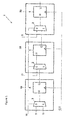
- the scan chain is schematically shown in Figure 1 .
- the scan chain comprises a plurality of scan blocks. In the example shown in Figure 1 , three scan blocks, 10, 20 and 30 are shown. In practice, the scan chains provided will be much larger.
- a scan chain can be any length. For example, some scan chains may have a very large number of scan blocks. Some scan chains may have tens of thousands of scan blocks.
- Each scan block is provided with a flip-flop or similar element.
- the flip-flop may be a D-type flip-flop.
- Each flip-flop 4 receives a clock signal at its clock input.
- a common clock signal is applied to each of the flip-flops.
- different flip-flops may receive different clock signals. Different ones of the scan blocks may be in different clock domains.
- Each scan block comprises a multiplexer 2.
- the multiplexer 2 has one input which is configured to receive data D.
- the other input is configured to receive a test input TI.
- the multiplexer 2 of the first scan block 10 is arranged to receive test data from the test data source.
- This data comprises a test vector in the form of a stream of data which is clocked through the serially connected flip-flops. Thus, the output of each flip-flop is connected to the test input of the next scan block and so on.
- a test enable signal is set to the scan mode. This causes the multiplexers 2 to select the test input data as the input to the flip-flop 4.
- the test vector is then scanned into this scan chain. In other words, in each successive clock cycle, the vector is shifted by one bit through the scan chain. At the end of the scan in mode, each flip-flop will have its respective bit of the test vector.
- the test enable signal is then de-asserted.
- the chip is put into the functional mode configuration which means that the data input of each multiplexer is selected.
- the outputs of functional circuitry are then captured by the respective flip-flops.
- the scan chain is then put back in to the test mode and the values which are captured by the flip-flops are clocked out. This can be done at the same time that a new test vector is input.
- Scan testing is used for testing digital integrated circuits.
- ATPG tools from CAD (computer aided design) vendors are used to generate the scan test patterns used with arrangements such as shown in Figure 1 .
- VLSI (very large scale integration) testers are used to apply these scan test patterns to the device under test (DUT).
- DUT device under test
- VLSI (very large scale integration) testers are used to apply these scan test patterns to the device under test (DUT).
- DUT device under test
- one or more devices are data logged. This may generate information such as a text file containing diagnostic failure data.
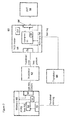
- FIG. 2 schematically shows a testing arrangement.
- An ATPG tool 50 is provided.
- the ATPG tools create scan test patterns which can be saved out, for example in one or more industry standard formats.
- WGL wave generation language
- STIL standard test interface language
- STIL is defined in IEEE P1450.1.
- the test patterns may be stored in a memory 66 of the ATPG tool.
- VLSI testers cannot directly use these standard file formats or other outputs of the ATPG tool.
- the tester manufacturer or third party vendors may supply tools which read in the scan patterns from the ATPG tool, and then write out one or more files in the specific format required by the specific tester. Accordingly a translation function 52 is provided between the ATPG tool 50 and the VLSI tester 54.
- the ATPG tool has an output 68 from which the test patterns are output to the translator.
- the ATPG has a test pattern generator 51 which create scan test patterns composed of multiple vectors.
- a vector may correspond to one clock cycle, and contains the test values (for example both drive and compare) for a set of channels which may correspond one to one to the pins on the IC being tested.
- the test patterns are stored in the memory 66.
- the VLSI tester 54 is used to apply scan test patterns via an interface 64 to the IC to be tested 58.
- the testing of an IC is performed by a test program.
- a test program may be made up from a set of DC tests and test patterns.
- the test patterns may include one or more of patterns testing the IC configured in the scan test mode, patterns testing the IC with the IC configured in a device specific test mode, and patterns testing the IC in its normal functional mode.
- the VLSI tester 54 receives from the translator the translated test patterns via an interface 62 and stores the (translated) test patterns in a test vector memory 56.
- Each test vector may contain one or more values which determine whether the pin electronics for each channel (which connect to the pins of the IC) generate high or low drive data, generate a high going or low going clock pulse, test for a high value, a low value, or a tristate value, or do not drive and do not test in each cycle.
- a master clock source 61 (which may be programmable) applies each set of data from the test vector memory to the device under test (DUT), until the vectors are exhausted. This may be indicated by a special value, terminal count, opcode or in any other suitable way.
- test vectors stored in the memory 56 of the tester 54 are applied by the tester 54 to the device under test.
- the response to each test vector is read out by the VLSI tester via the interface 64 and compared by a comparator 55 of the VLSI tester to an expected response stored in the memory 56.
- the comparison carried out by the comparator may be done dynamically as the test vector is read in. If the response of the device to the stimulus from the test vector memory matches the expected values also found in the test vector memory, the DUT is considered to have passed this test.
- the expected response is provided by the ATPG tool.
- the expected response will also be translated by the translator before being provided to the tester 54 and stored in the memory 56.
- the expected response may be provided with the test patterns or separately from the test patterns.
- the memory 56 may be provided by a plurality of memories.
- the VLSI tester 54 will generate a datalog or other suitable information.
- the datalog may be generated by a processing function 57 of the comparator 55.
- one or more separate processors may be provided to generate the datalog.
- the processing function or processors are provided by suitable processing circuitry.
- the datalog may be a file which contains fail information.
- the file may be a text file.
- Datalog formats can vary from each tester manufacturer.
- a datalog may contain one or more of a list of channels/pins which have had one or more mis-compares, the cycle number of each fail, together with the actual data value, sometimes giving the expected data value.
- the ATPG tool may have an analyser 53 which is configured to receive, for example, scan test fails (for example in an ATPG specific non-standard format) via input 70 and using the original scan test pattern, the ATPG tool performs an analysis to try to diagnose the cause of the fail.
- the information or datalog from the VLSI tester may be converted by a translator 60 to the file format expected by the ATPG tool.
- test time execution time of the test
- test vector memory usage the lower the execution time and/or the lower the amount of test vector memory usage the better.
- the flops are re-configured into serial scan chains which are repeatedly loaded with test data and unloaded with test results.
- the total number of flip flops in system on chips has increased at a faster rate than the ability to efficiently inject scan test data into these flip flops, because more scan flip flops result in longer scan chains, hence longer test times and greater test vector memory usage.
- Some embodiments may use time division multiplexing to multiply the number of input channels available for scan test purposes. This may provide an increase in the number of scan chains. This may result in an improvement in test efficiency.
- the flip flops which are used in the functional circuitry are reconfigured into one (or usually more) more serial shift registers providing one or more scan chains.
- digital I/O (input/output) pads are reconfigured into scan I/O pads known as scan inputs and scan outputs.
- scan inputs are used to inject data into the scan chains - there being a one to one correspondence in the number of scan inputs to the number of scan chains. Likewise there is a one to one correspondence in the number of scan outputs to the number of scan chains.
- some digital I/O pads are used as for a scan clocks, scan reset, and scan control.
- a standard scan control pad would be known as scan enable, and has the function of switching all the scan flip flops between the functional configuration and the serial shift register ("scan mode”) configuration.
- Some embodiments may be used with either of the previously mentioned architectures.
- a requirement associated with scan testing is the number of clock cycles required to load all the scan chains.
- the length of all the scan chains may be balanced between the number of available scan ports (a scan port provides one scan input and one scan output).
- Some available scan I/O are used for scan clocks, scan resets and scan control. The remaining scan I/O may be split in half and used as scan inputs and scan outputs. However, as SoCs get bigger, then usually more scan I/O are used for scan clocks, which then limits the number of scan I/O available for scan chains.
- the number of flip flops in the IC is nf and the number of scan in and scan out pairs (scan ports, usually the same number as number of scan chains) is ns, then the number of clock cycles required to load the scan chains with data would be nf/ns assuming a perfectly balanced set of scan chains.
- the scan chains are loaded and unloaded multiple (for example thousands) of times, hence the maximum length of the scan chains is of importance.
- the VLSI testers have a test vector memory into which many test data values are loaded. This memory is of limited size, but is often the most costly part of any VLSI tester. Each line of test vector memory maps to a single clock cycle during application of the test pattern to the device under test (DUT).
- Each scan test pattern is made up a test initialisation phase whose purpose is to put the IC into the scan testing mode, and a sequence of scan chain loads, scan capture test and scan chain unloads.
- the dominant usage of clock cycles and hence test vector memory is the scan chain load/unload (approximately nf/ns for well balanced scan chains).
- the time required to apply the test vectors to the DUT is directly proportional to the total number of test vectors used.
- the dominant factor which determines the number of scan test vectors is the load/unload cycles, which itself is determined by the scan chain length.
- One way to reduce the (maximum) scan chain length is to allocate more scan I/O pads to scan input and scan output usage (i.e. increase ns). However, this may mean that the number of scan I/O allocated to scan clock and scan reset usage, has to be reduced.
- clock domains The circuits which are clocked by the same clock frequency are known as "clock domains".
- clock domains The circuits which are clocked by the same clock frequency are known as "clock domains".
- one scan I/O scan clock pad may be allocated to each of the different internal clock domains. This requirement is a consequence of the different depths of clock tree for each of the clock domains. If the same scan clock were to be used for multiple clock domains, this may lead to a timing hazard during the scan capture phase of scan testing known as "shoot -through".
- This problem may be addressed by balancing the clock trees which are connected to the same scan clock, however there can be a high cost in silicon clock tree buffer overhead to achieve this. Consequently as the number of functional clock domains increase, the number of scan I/O needed to be allocated to scan clock usage may also increase.
- Some embodiments may provide circuitry which may increase the number of both scan inputs and scan clocks and resets.
- the circuitry allows a scan I/O pad to be used as both a scan input and a scan clock/reset.
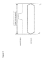
- Figure 3 shows the relationship between scan input timing and scan clock timing.
- the tester cycle or period is between time to and t 1 .
- the first line shows the scan clock which is pulsed high and then low again during the cycle.
- the scan inputs are shown on the second line and are all driven with a '0' or a '1' value at the start of each shift cycle.
- the scan input data propagates through the scan in pad (which is configured into the input mode during the shift phase of testing) and eventually reaches the test input (SI) of the first scan flip flop in a scan chain.
- the scan clock propagates through the scan clock pad (which is configured into the input mode for all phases of scan testing) then sometimes through some test multiplexing and onto a functional clock tree and thereby to a set of scan (and possibly non-scan) flip flops.
- Figure 4 shows the arrangement between the scan clock pad 104 and scan in pad 102 and the first flip flop 100 in the scan chain.
- the flip flop has a normal data input D; a normal data output Q; a clock pin CK; a scan enable input SE; a scan input SI; and a scan output SO.
- the flip flop may have a reset pin (not shown).
- a second scan flip flop 100 having the same inputs and outputs as the first flip flop.
- the first and second flip flops have the same scan clock.
- the scan out SO output of the first flip flop is provided to the scan in SI port of the second flip flop.
- Test "glue” circuitry 114 is provided between the scan in pad and the first flip flop.
- a first buffer 106 is provided for input signals between the scan in pad 102 and the test glue circuitry.
- a second buffer 108 is provided for output signals between the test glue circuitry 114 and the scan in pad.
- Test glue circuitry 116 is provided between and the scan clock pad and the clock inputs of the flip flops.
- a third buffer 110 is provided for input signals and a fourth buffer 112 is provided for output signals. The third and fourth buffers 110 and 112 are provided between the scan clock pad and the test glue circuitry 116.
- the test glue circuitry may be multiplexing circuitry in the pad logic which is enabled by test signals internal to the SoC and which when asserted put the pads into the scan configuration.
- the SE input of all flip flops would normally all be connected to the same internal test signal called scan enable or shift enable.
- This signal is set to '1' in order to enable the scan shift configuration and is set to '0' for the scan capture (or functional) configuration.
- the scan enable may be controlled by a dedicated scan test pad.
- the test glue circuitry is used such that the internal scan enable is low during the functional operation of the IC.
- the first flip flop in the scan chain has a more complicated timing requirement than flip flops internal to the scan chain because of the time it takes scan data to propagate from the pad to the first flip flop which in an IC might be some distance away.
- the digital pad re-purposed as a scan clock is put into the input mode during the application of all scan patterns, which includes scan shift and the testing phase known as scan capture.
- the digital pad re-purposed as a scan input is put into the input mode only during scan shift.
- the internal scan enable is shown as enabling this pad mode.
- Test glue circuitry 126 is provided with a first buffer 122 and a second buffer 124 between the test glue circuitry and the scan input and clock pad 120.
- the first buffer is for input data and the second buffer is for output data.
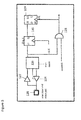
- An additional flip-flop 130 and a two input AND gate 128 is provided per scan in/clock pad.
- the flip flop 130 is shown as having in input D which receives an output of the test glue 126 and an output which is provided the scan input SI of the first flip flop 100 of the scan chain.
- the clock input of the flip flop 120 is clkX which will be described later in more detail.
- the AND gate 128 has its output provided to the clock input of each of the flip flops of the scan chain.
- the AND gate has a first input enable X which will be described later in more detail and a second input which is provide by the test glue.
- the test glue is controlled by a scan mode signal.
- Each scan I/O modified in this way can be used as a scan clock and a scan input.
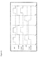
- Figure 6 shows a timing diagram for the arrangement of Figure 5 .
- the first line shows the pad signals
- the second line shows the signal enable X
- the third line shows the virtual scan clock (the scan clock output by the AND gate
- the fourth link shows clkX
- the fifth line shows the virtual scan input (the output provided by the flip flop 130.
- the timing diagram shows the required waveforms and timing of clkX and enable X in order to generate the derived virtual scan input and virtual scan clock.
- four tester cycles are shown. This equates to two virtual scan cycles.
- the first two cycles show the waveform required on the shared pad which will make the virtual scan input '1' while generating a clock pulse on the virtual scan clock.
- the enable X signal is low for the first cycle and high for the second cycle.
- the clock signal clkX will be low for the first half of the first cycle and high for the second half and is low for the whole of the second cycle.
- the virtual scan input will thus be low for the first half of the first cycle (because the clock signal is low) but will be high in the second half of the first cycle because the clock signal clkX is high and the pad signal is high.
- the virtual scan input remains high for the second cycle while the clkX is low.
- the next two cycles show the waveform required on the shared pad which will make the virtual scan input '0' while generating a clock pulse on the virtual scan clock.
- the input to the pad is low and in the fourth cycle the input is toggled from low to high and back to low again.
- the enable X signal is low for the third cycle and high for the fourth cycle.
- This means the output of the AND gate (virtual scan clock) is low for the third cycle and will go high in the fourth cycle when the pad signal is high.
- the clock signal clkX will be low for the first half of the third cycle and high for the second half and is low for the whole of the fourth cycle.
- the virtual scan input will thus be high for the first half of the third cycle (because the clock signal is still low) but will be low in the second half of the third cycle because the clock signal clkX is high and the pad signal is low.
- the virtual scan input remains low for the fourth cycle while the clkX is low.
- the gain of number of virtual scan inputs and virtual scan clocks may be at the expense of the number of test vectors (which is doubled). This may be acceptable for devices with smaller test vector requirements.
- the waveform on the (shared) pad may compatible with all tester types.
- Figure 7 shows a timing diagram waveforms and timing of clkX and enableX in order to generate the derived virtual scan input and virtual scan clock on a more timing flexible tester.
- the first line shows the pad signals
- the second line shows the signal enable X
- the third line shows the virtual scan clock (the scan clock output by the AND gate)
- the fourth link shows clkX
- the fifth line shows the virtual scan input (the output provided by the flip flop 130).
- the first cycle shows the waveform required on the shared pad which will make the virtual scan input '1' while generating a clock pulse on the virtual scan clock.
- the enable X signal is low for the first half of the first cycle and high for the second half of the first cycle. This means the output of the AND gate (virtual scan clock) is low for the first half of the first cycle and will go high in the second half of the first cycle when the pad signal is high.
- the clock signal clkX will be low for the first quarter of the first cycle and high for the second quarter and is low for the whole of the second half of the first cycle.
- the virtual scan input will thus be low for the first quarter of the first cycle (because the clock signal is low) but will be high in the remainder of the first cycle because the clock signal clkX is high and the pad signal is high.
- the virtual scan input remains high for the second half of the first cycle while the clkX is low.
- the next cycle shows the waveform required on the shared pad which will make the virtual scan input '0' while generating a clock pulse on the virtual scan clock.
- the input to the pad is low and in the last half of the cycle the input is toggled from low to high and back to low again.
- the enable X signal is low for the first half of the second cycle and high for the second half of the cycle. This means the output of the AND gate (virtual scan clock) is low for the first half of the second cycle and will go high in the second half of the second cycle when the pad signal is high.
- the clock signal clkX will be low for the first quarter of the second cycle, high for the second quarter and is low for the whole of the second half of the second cycle.
- the virtual scan input will thus be high for the first quarter of the second cycle (because the clock signal is still low) but will be low in the rest of the second cycle, because the clock signal clkX is high and the pad signal is low and then clkX is low.
- the required sequencing or timing setup time of the virtual scan input before the virtual scan clock is maintained in this example.
- Embodiments may be used with a tester having the capability of generating several events per cycle.
- the waveform shape on pad in cycle one appears like a double clock pulse, whereas the waveform shape on pad in cycle two appears like a single clock pulse.
- a number of testers have the capability of generating one or more clock pulses per tester cycle. Some embodiments may make use of the capability of this type of tester.
- enableX and clkX would both come from dedicated re-purposed digital I/O pads which are configured into input mode by the test signal scan mode.
- the necessary waveforms for these two test signals are straight forward for any test system to generate regardless of the type or capability of the tester.
- the delay from these auxiliary scan test pads to all the gating AND gates 128 and all the latching flip flops 130 is kept low and well balanced. Dedicating two scan test pads to be used to generate these enableX and clkX may not be a large overhead.
- suitable circuitry may be provided by a device under test to generate clkX and enable X.
- the ATPG tool is configured to generate the test pattern data which comprises scan data merged with the clock signal for application to the same input pad.
- the test pattern data is generated by the test pattern generator 71.
- the ATPG tool may not have the capability to merge the scan data and the clock signal such that the scan data is multiplexed with the clock data when the test pattern is applied to a scan pad.
- an additionally translator may be provided between the output of the ATPG tester and the input to the translator 52 which would merge the scan and clock data.
- the translator 52 may have the capability to merge the scan data and the clock signal.
- a CAD/EDA (electronic design automation) tool may have the ability to insert circuitry such as previously described in a circuit design. This may be done automatically, for example during scan insertion/hook-up.
- the device under test has been described as an integrated circuit. In other embodiments, the device under test may be a die.
Landscapes
- Engineering & Computer Science (AREA)
- General Engineering & Computer Science (AREA)
- Physics & Mathematics (AREA)
- General Physics & Mathematics (AREA)
- Computer Hardware Design (AREA)
- Tests Of Electronic Circuits (AREA)
- Semiconductor Integrated Circuits (AREA)
Abstract
Description
- Some embodiments relate to a circuit, and in particular but not exclusively which may be used for testing. The circuit may be provided in the integrated circuit or die. Some embodiments may relate to a method of testing an integrated circuit. Some embodiments may relate to an apparatus for testing an integrated circuit.
- Despite advances in semiconductor process technology integrated circuits can be manufactured with faults. Just a single fault can render a circuit unusable and because of this manufacturers have implemented various techniques to identify where these circuits are faulty.
- Integrated circuits can be tested by automated test equipment (ATE). The automated test equipment (ATE) typically works in response to a test sequence or input provided from an automatic test pattern generator (ATPG) which when applied to the circuit under test allows a distinction to be made between correct circuit behaviour and faulty circuit behaviour. ATPG patterns can in practice be used to attempt to detect faults such as a "stuck-at fault" where a signal line in the circuit is assumed to be stuck at a fixed logic value regardless of the inputs supplied to the circuit.
- As integrated circuits have become larger, the amount of test circuitry required may be increased.
- According to one aspect, there is provided an integrated circuit or die comprising: a first input pad configured to receive an input, said first input pad input comprises scan data multiplexed with a clock signal; a scan chain configured to receive said scan data and said clock signal, a circuit provided between said first input pad and said scan chain configured to provide from said input a first output and a second output, said first output providing said scan data and said second output providing said clock signal.
- The circuit may comprise a first part having an enable input and a second input to receive said first input pad input, said first part being configured to provide said second output.
- The first part may comprise a logic gate, said enable inputs and said second inputs being inputs to said gate and said second output being an output of said gate.
- The logic gate may comprise an AND gate.
- The circuit may comprise a second part having a data input and configured to provide said first output.
- The second part may comprise a flip flop, a data input of said flip flop configured to receive said first input pad input and a data output of said flip flop configured to provide said first output.
- The second part may be configured to receive a control clock input.
- A clock input of said flip flop may be configured to receive said control clock input.
- At least one of said control clock input and said enable input may be provided by one or more input pads different to said first input pad.
- The input may be received from a tester and one tester cycle may be required to provide one value of said scan data and its associated clock signal.
- The input may be received from a tester and two tester cycles may be required to provide one value of said scan data and its associated clock signal.
- According to another aspect, there is provided a tester apparatus comprising: a test pattern generator configured to generate test pattern data for testing of an integrated circuit or die having a first input pad configured to receive an input, said generated test pattern data comprising said scan data multiplexed with said clock data for applying to said first input pad; a memory configured to store said scan test pattern; and an output configured to output said generated test pattern data.
- According to another aspect, there is provided a method comprising: applying an input to a first input pad of an integrated circuit or die, said input comprising scan data multiplexed with a clock signal, wherein one or two tester cycles is required to provide one value of said scan data and its associated clock signal.
- According to another aspect, there is provided a tester apparatus comprising: a memory configured to store test data to be applied to a first input pad of an integrated circuit or die, said test data comprising scan data multiplexed with a clock signal, an output configured to output said test data to said first input pad, wherein one or two tester cycles is required to provide one value of said scan data and its associated clock signal.
- A computer program comprising program code means adapted to perform the method may also be provided. The computer program may be stored and/or otherwise embodied by means of a carrier medium.
- In the above, many different embodiments have been described. It should be appreciated that further embodiments may be provided by the combination of any two or more of the embodiments described above.
- Various other aspects and further embodiments are also described in the following detailed description and in the attached claims.
- For a better understanding of some embodiments, reference will now be made by way of example only to the accompanying Figures in which:
-
Figure 1 schematically shows a scan chain; -
Figure 2 schematically shows a test environment; -
Figure 3 shows a test cycle; -
Figure 4 shows schematically part of an integrated circuit or die; -
Figure 5 shows schematically part of an integrated circuit or die of an embodiment; -
Figure 6 shows a first timing diagram for the arrangement ofFigure 5 ; and -
Figure 7 shows a second timing diagram for the arrangement ofFigure 5 . - Some embodiments may have scan chains for testing system on chip circuits or the like. Reference is made to
Figure 1 which schematically shows an integrated circuit or die 1 with a scan chain. The scan chain is schematically shown inFigure 1 . The scan chain comprises a plurality of scan blocks. In the example shown inFigure 1 , three scan blocks, 10, 20 and 30 are shown. In practice, the scan chains provided will be much larger. A scan chain can be any length. For example, some scan chains may have a very large number of scan blocks. Some scan chains may have tens of thousands of scan blocks. - Each scan block is provided with a flip-flop or similar element. In some embodiments, the flip-flop may be a D-type flip-flop. Each flip-
flop 4 receives a clock signal at its clock input. In the example shown inFigure 1 , a common clock signal is applied to each of the flip-flops. However, it should be appreciated that in some embodiments, different flip-flops may receive different clock signals. Different ones of the scan blocks may be in different clock domains. - Each scan block comprises a
multiplexer 2. Themultiplexer 2 has one input which is configured to receive data D. The other input is configured to receive a test input TI. Themultiplexer 2 of thefirst scan block 10 is arranged to receive test data from the test data source. This data comprises a test vector in the form of a stream of data which is clocked through the serially connected flip-flops. Thus, the output of each flip-flop is connected to the test input of the next scan block and so on. - In order to put the scan chain into the scan mode, a test enable signal is set to the scan mode. This causes the
multiplexers 2 to select the test input data as the input to the flip-flop 4. The test vector is then scanned into this scan chain. In other words, in each successive clock cycle, the vector is shifted by one bit through the scan chain. At the end of the scan in mode, each flip-flop will have its respective bit of the test vector. The test enable signal is then de-asserted. - The chip is put into the functional mode configuration which means that the data input of each multiplexer is selected. The outputs of functional circuitry are then captured by the respective flip-flops. The scan chain is then put back in to the test mode and the values which are captured by the flip-flops are clocked out. This can be done at the same time that a new test vector is input.
- Scan testing is used for testing digital integrated circuits. ATPG tools from CAD (computer aided design) vendors are used to generate the scan test patterns used with arrangements such as shown in
Figure 1 . - VLSI (very large scale integration) testers are used to apply these scan test patterns to the device under test (DUT). During the development of the test program or during the testing of first silicon, or during the analysis of production issues, one or more devices are data logged. This may generate information such as a text file containing diagnostic failure data.
- Reference is now made to
Figure 2 which schematically shows a testing arrangement. AnATPG tool 50 is provided. The ATPG tools create scan test patterns which can be saved out, for example in one or more industry standard formats. WGL (wave generation language) and STIL (standard test interface language) are two examples of industry standard file formats which are defined. For example STIL is defined in IEEE P1450.1. The test patterns may be stored in amemory 66 of the ATPG tool. - However, many VLSI testers cannot directly use these standard file formats or other outputs of the ATPG tool. The tester manufacturer or third party vendors may supply tools which read in the scan patterns from the ATPG tool, and then write out one or more files in the specific format required by the specific tester. Accordingly a
translation function 52 is provided between theATPG tool 50 and theVLSI tester 54. The ATPG tool has anoutput 68 from which the test patterns are output to the translator. - The ATPG has a
test pattern generator 51 which create scan test patterns composed of multiple vectors. A vector may correspond to one clock cycle, and contains the test values (for example both drive and compare) for a set of channels which may correspond one to one to the pins on the IC being tested. The test patterns are stored in thememory 66. - The
VLSI tester 54 is used to apply scan test patterns via aninterface 64 to the IC to be tested 58. The testing of an IC is performed by a test program. A test program may be made up from a set of DC tests and test patterns. The test patterns may include one or more of patterns testing the IC configured in the scan test mode, patterns testing the IC with the IC configured in a device specific test mode, and patterns testing the IC in its normal functional mode. - The
VLSI tester 54 receives from the translator the translated test patterns via aninterface 62 and stores the (translated) test patterns in atest vector memory 56. Each test vector may contain one or more values which determine whether the pin electronics for each channel (which connect to the pins of the IC) generate high or low drive data, generate a high going or low going clock pulse, test for a high value, a low value, or a tristate value, or do not drive and do not test in each cycle. - There is normally one to one correspondence to the vectors found in the ATPG scan test patterns and the translated data stored in the
test vector memory 56 of the tester. - A master clock source 61 (which may be programmable) applies each set of data from the test vector memory to the device under test (DUT), until the vectors are exhausted. This may be indicated by a special value, terminal count, opcode or in any other suitable way.
- The test vectors stored in the
memory 56 of thetester 54 are applied by thetester 54 to the device under test. The response to each test vector is read out by the VLSI tester via theinterface 64 and compared by acomparator 55 of the VLSI tester to an expected response stored in thememory 56. In some embodiments, the comparison carried out by the comparator may be done dynamically as the test vector is read in. If the response of the device to the stimulus from the test vector memory matches the expected values also found in the test vector memory, the DUT is considered to have passed this test. - The expected response is provided by the ATPG tool. The expected response will also be translated by the translator before being provided to the
tester 54 and stored in thememory 56. The expected response may be provided with the test patterns or separately from the test patterns. - In some embodiments the
memory 56 may be provided by a plurality of memories. - There may be many reasons why the application of a scan test pattern to a DUT would result in a fail result. In the cases where an analysis of the cause of the failure of the scan test pattern is required, the
VLSI tester 54 will generate a datalog or other suitable information. In some embodiments, the datalog may be generated by aprocessing function 57 of thecomparator 55. Alternatively or additionally, in other embodiments, one or more separate processors may be provided to generate the datalog. The processing function or processors are provided by suitable processing circuitry. - The datalog may be a file which contains fail information. The file may be a text file. Datalog formats can vary from each tester manufacturer. A datalog may contain one or more of a list of channels/pins which have had one or more mis-compares, the cycle number of each fail, together with the actual data value, sometimes giving the expected data value.
- The ATPG tool may have an
analyser 53 which is configured to receive, for example, scan test fails (for example in an ATPG specific non-standard format) viainput 70 and using the original scan test pattern, the ATPG tool performs an analysis to try to diagnose the cause of the fail. The information or datalog from the VLSI tester may be converted by atranslator 60 to the file format expected by the ATPG tool. - As digital integrated circuits have become larger, there may be an issue with the efficiency of test, which can measured in terms of test time (execution time of the test) and/or test vector memory usage. Generally the lower the execution time and/or the lower the amount of test vector memory usage the better.
- During scan testing the flops are re-configured into serial scan chains which are repeatedly loaded with test data and unloaded with test results.
- The total number of flip flops in system on chips has increased at a faster rate than the ability to efficiently inject scan test data into these flip flops, because more scan flip flops result in longer scan chains, hence longer test times and greater test vector memory usage.
- Some embodiments may use time division multiplexing to multiply the number of input channels available for scan test purposes. This may provide an increase in the number of scan chains. This may result in an improvement in test efficiency.
- In the scan testing configuration the flip flops which are used in the functional circuitry are reconfigured into one (or usually more) more serial shift registers providing one or more scan chains. In the scan testing configuration, digital I/O (input/output) pads are reconfigured into scan I/O pads known as scan inputs and scan outputs.
- In one example, scan inputs are used to inject data into the scan chains - there being a one to one correspondence in the number of scan inputs to the number of scan chains. Likewise there is a one to one correspondence in the number of scan outputs to the number of scan chains. In the scan testing configuration some digital I/O pads are used as for a scan clocks, scan reset, and scan control. A standard scan control pad would be known as scan enable, and has the function of switching all the scan flip flops between the functional configuration and the serial shift register ("scan mode") configuration.
- There are other scan architectures in which the number of scan inputs does not match the number of scan chains. In these examples additional test circuitry has been added to decompress the scan in data and/or compress the scan out data or other unique scan test architectures.
- Some embodiments may be used with either of the previously mentioned architectures.
- Generally, it may be advantageous to have as many digital I/O pins re-purposed for scan purposes as possible. A requirement associated with scan testing is the number of clock cycles required to load all the scan chains. Generally, the length of all the scan chains may be balanced between the number of available scan ports (a scan port provides one scan input and one scan output).
- Some available scan I/O are used for scan clocks, scan resets and scan control. The remaining scan I/O may be split in half and used as scan inputs and scan outputs. However, as SoCs get bigger, then usually more scan I/O are used for scan clocks, which then limits the number of scan I/O available for scan chains.
- If the number of flip flops in the IC is nf and the number of scan in and scan out pairs (scan ports, usually the same number as number of scan chains) is ns, then the number of clock cycles required to load the scan chains with data would be nf/ns assuming a perfectly balanced set of scan chains. During the scan test of a SoC the scan chains are loaded and unloaded multiple (for example thousands) of times, hence the maximum length of the scan chains is of importance.
- The problem encountered in testing ICs is that for each new generation of IC which increases in linear size by a factor of X, the number of flip flops nf is increasing at a faster rate (proportional to X2) as compared to the number of pads and hence number of scan ports ns (which increases proportional to X).
- The VLSI testers have a test vector memory into which many test data values are loaded. This memory is of limited size, but is often the most costly part of any VLSI tester. Each line of test vector memory maps to a single clock cycle during application of the test pattern to the device under test (DUT).
- Each scan test pattern is made up a test initialisation phase whose purpose is to put the IC into the scan testing mode, and a sequence of scan chain loads, scan capture test and scan chain unloads. The dominant usage of clock cycles and hence test vector memory is the scan chain load/unload (approximately nf/ns for well balanced scan chains). The time required to apply the test vectors to the DUT is directly proportional to the total number of test vectors used. The dominant factor which determines the number of scan test vectors is the load/unload cycles, which itself is determined by the scan chain length.
- One way to reduce the (maximum) scan chain length is to allocate more scan I/O pads to scan input and scan output usage (i.e. increase ns). However, this may mean that the number of scan I/O allocated to scan clock and scan reset usage, has to be reduced.
- For some ICs the number of scan I/O which need to be allocated to scan clocks and scan resets is also increasing as a result of more complicated IC architecture.
- Inside a complicated IC often many circuits need to be clocks at different frequencies, often to meet industry standards (e.g. USB, PCI). The circuits which are clocked by the same clock frequency are known as "clock domains". During scan testing, one scan I/O scan clock pad may be allocated to each of the different internal clock domains. This requirement is a consequence of the different depths of clock tree for each of the clock domains. If the same scan clock were to be used for multiple clock domains, this may lead to a timing hazard during the scan capture phase of scan testing known as "shoot -through". This problem may be addressed by balancing the clock trees which are connected to the same scan clock, however there can be a high cost in silicon clock tree buffer overhead to achieve this. Consequently as the number of functional clock domains increase, the number of scan I/O needed to be allocated to scan clock usage may also increase.
- Thus more scan clocks and/or more scan chains may be required to minimise test time, but the number of scan I/O is limited and shared between the two competing requirements.
- Some embodiments may provide circuitry which may increase the number of both scan inputs and scan clocks and resets. The circuitry allows a scan I/O pad to be used as both a scan input and a scan clock/reset.
- Consequently this may allow a greater number of scan chains and this in turn allows the maximum scan chain length to be reduced, resulting in reduced test vector usage, which in turn may lead to greater scan test efficiency and reduced test time.
- Some embodiments take advantage of the standard order of events found during scan shift
-
Figure 3 shows the relationship between scan input timing and scan clock timing. The tester cycle or period is between time to and t1. The first line shows the scan clock which is pulsed high and then low again during the cycle. - The scan inputs are shown on the second line and are all driven with a '0' or a '1' value at the start of each shift cycle.
- In some scan architectures, the scan input data propagates through the scan in pad (which is configured into the input mode during the shift phase of testing) and eventually reaches the test input (SI) of the first scan flip flop in a scan chain. The scan clock propagates through the scan clock pad (which is configured into the input mode for all phases of scan testing) then sometimes through some test multiplexing and onto a functional clock tree and thereby to a set of scan (and possibly non-scan) flip flops.
-
Figure 4 shows the arrangement between thescan clock pad 104 and scan inpad 102 and thefirst flip flop 100 in the scan chain. The flip flop has a normal data input D; a normal data output Q; a clock pin CK; a scan enable input SE; a scan input SI; and a scan output SO. The flip flop may have a reset pin (not shown). A secondscan flip flop 100 having the same inputs and outputs as the first flip flop. The first and second flip flops have the same scan clock. The scan out SO output of the first flip flop is provided to the scan in SI port of the second flip flop. - Test "glue"
circuitry 114 is provided between the scan in pad and the first flip flop. Afirst buffer 106 is provided for input signals between the scan inpad 102 and the test glue circuitry. Asecond buffer 108 is provided for output signals between thetest glue circuitry 114 and the scan in pad.Test glue circuitry 116 is provided between and the scan clock pad and the clock inputs of the flip flops. Athird buffer 110 is provided for input signals and afourth buffer 112 is provided for output signals. The third andfourth buffers test glue circuitry 116. - The test glue circuitry may be multiplexing circuitry in the pad logic which is enabled by test signals internal to the SoC and which when asserted put the pads into the scan configuration.
- The SE input of all flip flops would normally all be connected to the same internal test signal called scan enable or shift enable. This signal is set to '1' in order to enable the scan shift configuration and is set to '0' for the scan capture (or functional) configuration. The scan enable may be controlled by a dedicated scan test pad. The test glue circuitry is used such that the internal scan enable is low during the functional operation of the IC.
- The first flip flop in the scan chain has a more complicated timing requirement than flip flops internal to the scan chain because of the time it takes scan data to propagate from the pad to the first flip flop which in an IC might be some distance away.
- The digital pad re-purposed as a scan clock is put into the input mode during the application of all scan patterns, which includes scan shift and the testing phase known as scan capture.
- The digital pad re-purposed as a scan input is put into the input mode only during scan shift. In the
Figure 4 , the internal scan enable is shown as enabling this pad mode. - In the embodiments which will be described now, have circuitry whereby the same pads can be used for both scan input purposes and also scan clock purposes. This may allow more scan input and scan output pairs, which in turn should lead to a reduced scan chain length, and the resulting efficiencies.
- Reference is made to
Figure 5 which shows a single pad providing a scan input and clock pad.Test glue circuitry 126 is provided with afirst buffer 122 and asecond buffer 124 between the test glue circuitry and the scan input andclock pad 120. The first buffer is for input data and the second buffer is for output data. An additional flip-flop 130 and a two input ANDgate 128 is provided per scan in/clock pad. Theflip flop 130 is shown as having in input D which receives an output of thetest glue 126 and an output which is provided the scan input SI of thefirst flip flop 100 of the scan chain. The clock input of theflip flop 120 is clkX which will be described later in more detail. The ANDgate 128 has its output provided to the clock input of each of the flip flops of the scan chain. The AND gate has a first input enable X which will be described later in more detail and a second input which is provide by the test glue. The test glue is controlled by a scan mode signal. Each scan I/O modified in this way can be used as a scan clock and a scan input. - Reference is made to
Figure 6 which shows a timing diagram for the arrangement ofFigure 5 . The first line shows the pad signals, the second line shows the signal enable X, the third line shows the virtual scan clock (the scan clock output by the AND gate, the fourth link shows clkX, the fifth line shows the virtual scan input (the output provided by theflip flop 130. - The timing diagram shows the required waveforms and timing of clkX and enable X in order to generate the derived virtual scan input and virtual scan clock. In this diagram four tester cycles are shown. This equates to two virtual scan cycles.
- The first two cycles show the waveform required on the shared pad which will make the virtual scan input '1' while generating a clock pulse on the virtual scan clock.
- In each of the first two cycles the input is toggled from low to high and back to low again. The enable X signal is low for the first cycle and high for the second cycle. This means the output of the AND gate (virtual scan clock) is low for the first cycle and will go high in the second cycle when the pad signal is high. The clock signal clkX will be low for the first half of the first cycle and high for the second half and is low for the whole of the second cycle. The virtual scan input will thus be low for the first half of the first cycle (because the clock signal is low) but will be high in the second half of the first cycle because the clock signal clkX is high and the pad signal is high. The virtual scan input remains high for the second cycle while the clkX is low.
- The next two cycles show the waveform required on the shared pad which will make the virtual scan input '0' while generating a clock pulse on the virtual scan clock.
- In the third cycle, the input to the pad is low and in the fourth cycle the input is toggled from low to high and back to low again. The enable X signal is low for the third cycle and high for the fourth cycle. This means the output of the AND gate (virtual scan clock) is low for the third cycle and will go high in the fourth cycle when the pad signal is high. The clock signal clkX will be low for the first half of the third cycle and high for the second half and is low for the whole of the fourth cycle. The virtual scan input will thus be high for the first half of the third cycle (because the clock signal is still low) but will be low in the second half of the third cycle because the clock signal clkX is high and the pad signal is low. The virtual scan input remains low for the fourth cycle while the clkX is low.
- It can be observed that the required sequencing or timing setup time of the virtual scan input before the virtual scan clock is maintained.
- In this example the gain of number of virtual scan inputs and virtual scan clocks may be at the expense of the number of test vectors (which is doubled). This may be acceptable for devices with smaller test vector requirements. The waveform on the (shared) pad may compatible with all tester types.
- Reference is made to
Figure 7 which shows a timing diagram waveforms and timing of clkX and enableX in order to generate the derived virtual scan input and virtual scan clock on a more timing flexible tester. The first line shows the pad signals, the second line shows the signal enable X, the third line shows the virtual scan clock (the scan clock output by the AND gate), the fourth link shows clkX, the fifth line shows the virtual scan input (the output provided by the flip flop 130). - In this Figure two tester cycles are shown. This equates directly to two virtual scan cycles.
- The first cycle shows the waveform required on the shared pad which will make the virtual scan input '1' while generating a clock pulse on the virtual scan clock. In the first cycles the input is toggled from low to high and back to low twice. The enable X signal is low for the first half of the first cycle and high for the second half of the first cycle. This means the output of the AND gate (virtual scan clock) is low for the first half of the first cycle and will go high in the second half of the first cycle when the pad signal is high. The clock signal clkX will be low for the first quarter of the first cycle and high for the second quarter and is low for the whole of the second half of the first cycle. The virtual scan input will thus be low for the first quarter of the first cycle (because the clock signal is low) but will be high in the remainder of the first cycle because the clock signal clkX is high and the pad signal is high. The virtual scan input remains high for the second half of the first cycle while the clkX is low.
- The next cycle shows the waveform required on the shared pad which will make the virtual scan input '0' while generating a clock pulse on the virtual scan clock.
- In the first half of the second cycle, the input to the pad is low and in the last half of the cycle the input is toggled from low to high and back to low again. The enable X signal is low for the first half of the second cycle and high for the second half of the cycle. This means the output of the AND gate (virtual scan clock) is low for the first half of the second cycle and will go high in the second half of the second cycle when the pad signal is high. The clock signal clkX will be low for the first quarter of the second cycle, high for the second quarter and is low for the whole of the second half of the second cycle. The virtual scan input will thus be high for the first quarter of the second cycle (because the clock signal is still low) but will be low in the rest of the second cycle, because the clock signal clkX is high and the pad signal is low and then clkX is low.
- The required sequencing or timing setup time of the virtual scan input before the virtual scan clock is maintained in this example.
- In this example the gain of number of virtual scan inputs and virtual scan clocks does not impact the test vector requirements. Embodiments may be used with a tester having the capability of generating several events per cycle.
- It can be observed that the waveform shape on pad in cycle one appears like a double clock pulse, whereas the waveform shape on pad in cycle two appears like a single clock pulse. A number of testers have the capability of generating one or more clock pulses per tester cycle. Some embodiments may make use of the capability of this type of tester.
- In one embodiment, enableX and clkX would both come from dedicated re-purposed digital I/O pads which are configured into input mode by the test signal scan mode. The necessary waveforms for these two test signals are straight forward for any test system to generate regardless of the type or capability of the tester.
- In some embodiments, the delay from these auxiliary scan test pads to all the gating AND
gates 128 and all the latchingflip flops 130 is kept low and well balanced. Dedicating two scan test pads to be used to generate these enableX and clkX may not be a large overhead. - In some embodiments, suitable circuitry may be provided by a device under test to generate clkX and enable X.
- In some embodiments, the ATPG tool is configured to generate the test pattern data which comprises scan data merged with the clock signal for application to the same input pad. The test pattern data is generated by the test pattern generator 71.
- In some embodiments, the ATPG tool may not have the capability to merge the scan data and the clock signal such that the scan data is multiplexed with the clock data when the test pattern is applied to a scan pad. In those embodiments, an additionally translator may be provided between the output of the ATPG tester and the input to the
translator 52 which would merge the scan and clock data. - In other embodiments, the
translator 52 may have the capability to merge the scan data and the clock signal. - A CAD/EDA (electronic design automation) tool may have the ability to insert circuitry such as previously described in a circuit design. This may be done automatically, for example during scan insertion/hook-up.
- The device under test has been described as an integrated circuit. In other embodiments, the device under test may be a die.
- Whilst this detailed description has set forth some embodiments of the present invention, the appended claims cover other embodiments of the present application which differ from the described embodiments according to various modifications and improvements. Other applications and configurations may be apparent to the person skilled in the art.
Claims (14)
- An integrated circuit or die comprising:a first input pad configured to receive an input, said first input pad input comprises scan data multiplexed with a clock signal,a scan chain configured to receive said scan data and said clock signal,a circuit provided between said first input pad and said scan chain configured to provide from said input a first output and a second output, said first output providing said scan data and said second output providing said clock signal.
- An integrated circuit or die as claimed in claim 1, wherein said circuit comprises a first part having an enable input and a second input to receive said first input pad input, said first part being configured to provide said second output.
- An integrated circuit or die as claimed in claim 2, wherein said first part comprises a logic gate, said enable inputs and said second inputs being inputs to said gate and said second output being an output of said gate.
- An integrated circuit or die as claimed in claim 3, wherein said logic gate comprises an AND gate.
- An integrated circuit or die as claimed in claim 2 or any claim appended thereto, wherein said circuit comprises a second part having a data input and configured to provide said first output.
- An integrated circuit or die as claimed in claim 5, wherein said second part comprises a flip flop, a data input of said flip flop configured to receive said first input pad input and a data output of said flip flop configured to provide said first output.
- An integrated circuit or die as claimed in claim 5 or 6 wherein said second part is configured to receive a control clock input.
- An integrated circuit or die as claimed in claim 7, when appended to claim 6, wherein a clock input of said flip flop is configured to receive said control clock input.
- An integrated circuit or die as claimed in claim 2 or 7, or any claim appended thereto, wherein at least one of said control clock input and said enable input is provide by one or more input pads different to said first input pad.
- An integrated circuit or die as claimed in any preceding claim, wherein said input is received from a tester and one tester cycle is required to provide one value of said scan data and its associated clock signal.
- An integrated circuit or die as claimed in any of claim 1 to 9, wherein said input is received from a tester and two tester cycles are required to provide one value of said scan data and its associated clock signal.
- A tester apparatus comprising:a test pattern generator configured to generate test pattern data for testing of an integrated circuit or die having a first input pad configured to receive an input, said generated test pattern data comprising said scan data multiplexed with said clock data for applying to said first input pad;a memory configured to store said scan test pattern; andan output configured to output said generated test pattern data.
- A method comprising:applying an input to a first input pad of an integrated circuit or die, said input comprising scan data multiplexed with a clock signal, wherein one or two tester cycles is required to provide one value of said scan data and its associated clock signal.
- A tester apparatus comprising:a memory configured to store test data to be applied to a first input pad of an integrated circuit or die, said test data comprising scan data multiplexed with a clock signal,an output configured to output said test data to said first input pad, wherein one or two tester cycles is required to provide one value of said scan data and its associated clock signal.
Applications Claiming Priority (1)
| Application Number | Priority Date | Filing Date | Title |
|---|---|---|---|
| GB1405520.6A GB2524560A (en) | 2014-03-27 | 2014-03-27 | A circuit for use in scan testing |
Publications (1)
| Publication Number | Publication Date |
|---|---|
| EP2924452A1 true EP2924452A1 (en) | 2015-09-30 |
Family
ID=50737531
Family Applications (1)
| Application Number | Title | Priority Date | Filing Date |
|---|---|---|---|
| EP15161196.9A Withdrawn EP2924452A1 (en) | 2014-03-27 | 2015-03-26 | A circuit for use in scan testing |
Country Status (3)
| Country | Link |
|---|---|
| US (1) | US9664738B2 (en) |
| EP (1) | EP2924452A1 (en) |
| GB (1) | GB2524560A (en) |
Families Citing this family (10)
| Publication number | Priority date | Publication date | Assignee | Title |
|---|---|---|---|---|
| US10498528B2 (en) * | 2016-06-30 | 2019-12-03 | AEMEA Inc. | Clock computing Machines |
| US10247777B1 (en) * | 2016-11-10 | 2019-04-02 | Teseda Corporation | Detecting and locating shoot-through timing failures in a semiconductor integrated circuit |
| US11194934B2 (en) * | 2017-06-21 | 2021-12-07 | AEMEA Inc. | Clock and periodic computing machines |
| US10761131B1 (en) * | 2018-09-25 | 2020-09-01 | Cadence Design Systems, Inc. | Method for optimally connecting scan segments in two-dimensional compression chains |
| US10746792B1 (en) * | 2018-11-30 | 2020-08-18 | Amazon Technologies, Inc. | Debug mechanisms for a processor circuit |
| US10976367B2 (en) * | 2018-12-13 | 2021-04-13 | Micron Technology, Inc. | Controller structural testing with automated test vectors |
| US12034445B2 (en) * | 2019-12-02 | 2024-07-09 | AEMEA Inc. | Clock and periodic computing machines |
| US11443823B2 (en) | 2020-10-29 | 2022-09-13 | SambaNova Systems, Inc. | Method and circuit for scan dump of latch array |
| US11449404B1 (en) | 2021-07-09 | 2022-09-20 | SambaNova Systems, Inc. | Built-in self-test for processor unit with combined memory and logic |
| US12493075B1 (en) | 2024-06-06 | 2025-12-09 | Stmicroelectronics International N.V. | Test pattern reset control circuit |
Citations (5)
| Publication number | Priority date | Publication date | Assignee | Title |
|---|---|---|---|---|
| US20030123489A1 (en) * | 2001-12-27 | 2003-07-03 | Ando Electric Co., Ltd. | Circuit for generating time division multiplex signal |
| US20050055617A1 (en) * | 2003-08-01 | 2005-03-10 | Laung-Terng Wang | Method and apparatus for shifting at-speed scan patterns in a scan-based integrated circuit |
| US20070033465A1 (en) * | 2005-07-15 | 2007-02-08 | Greenberg Craig B | Apparatus and method for a single wire interface between a intergated circuit and JTAG test and emulation apparatus |
| US20100313089A1 (en) * | 2008-07-18 | 2010-12-09 | Janusz Rajski | Scan Test Application Through High-Speed Serial Input/Outputs |
| WO2011059439A2 (en) * | 2009-11-12 | 2011-05-19 | Mentor Graphics Corporation | Scan test application through high-speed serial input/outputs |
Family Cites Families (7)
| Publication number | Priority date | Publication date | Assignee | Title |
|---|---|---|---|---|
| US6393592B1 (en) * | 1999-05-21 | 2002-05-21 | Adaptec, Inc. | Scan flop circuitry and methods for making the same |
| US6658363B2 (en) * | 2001-01-18 | 2003-12-02 | Hewlett-Packard Development Company, L.P. | Digital data pattern detection methods and arrangements |
| US7134061B2 (en) * | 2003-09-08 | 2006-11-07 | Texas Instruments Incorporated | At-speed ATPG testing and apparatus for SoC designs having multiple clock domain using a VLCT test platform |
| US7380185B2 (en) * | 2005-12-19 | 2008-05-27 | Texas Instruments Incorporated | Reduced pin count scan chain implementation |
| US7992062B2 (en) * | 2006-06-22 | 2011-08-02 | Qualcomm Incorporated | Logic device and method supporting scan test |
| CN102201800B (en) * | 2010-03-24 | 2014-03-19 | 台湾积体电路制造股份有限公司 | Integrated circuit and method of operation thereof |
| US9121892B2 (en) * | 2012-08-13 | 2015-09-01 | Analog Devices Global | Semiconductor circuit and methodology for in-system scan testing |
-
2014
- 2014-03-27 GB GB1405520.6A patent/GB2524560A/en not_active Withdrawn
-
2015
- 2015-03-26 US US14/670,033 patent/US9664738B2/en not_active Expired - Fee Related
- 2015-03-26 EP EP15161196.9A patent/EP2924452A1/en not_active Withdrawn
Patent Citations (5)
| Publication number | Priority date | Publication date | Assignee | Title |
|---|---|---|---|---|
| US20030123489A1 (en) * | 2001-12-27 | 2003-07-03 | Ando Electric Co., Ltd. | Circuit for generating time division multiplex signal |
| US20050055617A1 (en) * | 2003-08-01 | 2005-03-10 | Laung-Terng Wang | Method and apparatus for shifting at-speed scan patterns in a scan-based integrated circuit |
| US20070033465A1 (en) * | 2005-07-15 | 2007-02-08 | Greenberg Craig B | Apparatus and method for a single wire interface between a intergated circuit and JTAG test and emulation apparatus |
| US20100313089A1 (en) * | 2008-07-18 | 2010-12-09 | Janusz Rajski | Scan Test Application Through High-Speed Serial Input/Outputs |
| WO2011059439A2 (en) * | 2009-11-12 | 2011-05-19 | Mentor Graphics Corporation | Scan test application through high-speed serial input/outputs |
Also Published As
| Publication number | Publication date |
|---|---|
| GB2524560A (en) | 2015-09-30 |
| GB201405520D0 (en) | 2014-05-14 |
| US20150276874A1 (en) | 2015-10-01 |
| US9664738B2 (en) | 2017-05-30 |
Similar Documents
| Publication | Publication Date | Title |
|---|---|---|
| US9664738B2 (en) | Method and apparatus for improving efficiency of testing integrated circuits | |
| US8127187B2 (en) | Method and apparatus of ATE IC scan test using FPGA-based system | |
| US7653849B1 (en) | Input-output device testing including embedded tests | |
| US6446230B1 (en) | Mechanism for enabling compliance with the IEEE standard 1149.1 for boundary-scan designs and tests | |
| US10281524B2 (en) | Test partition external input/output interface control for test partitions in a semiconductor | |
| US8650524B1 (en) | Method and apparatus for low-pin count testing of integrated circuits | |
| US8904256B1 (en) | Method and apparatus for low-pin count testing of integrated circuits | |
| US11899063B2 (en) | Generating multiple pseudo static control signals using on-chip JTAG state machine | |
| US8479068B2 (en) | Decoded register outputs enabling test clock to selected asynchronous domains | |
| US11906582B2 (en) | Shadow access port method and apparatus | |
| US20160349320A1 (en) | Remote bus wrapper for testing remote cores using automatic test pattern generation and other techniques | |
| WO2007140366A2 (en) | Testing components of i/o paths of an integrated circuit | |
| WO2005006189A1 (en) | Automatic self test of an integrated circuit via ac i/o loopback | |
| Gillis et al. | Delay test of chip I/Os using LSSD boundary scan | |
| JP2006145527A (en) | Method and apparatus for embedded time domain reflectivity test | |
| US7519888B2 (en) | Input-output device testing | |
| US6061284A (en) | Core test control | |
| US20060041806A1 (en) | Testing method for semiconductor device and testing circuit for semiconductor device | |
| US20250271501A1 (en) | Circuit input/output (i/o) test system | |
| US10890619B2 (en) | Sequential test access port selection in a JTAG interface | |
| US11493553B2 (en) | Extended JTAG controller and method for functional reset using the extended JTAG controller | |
| JPH04221781A (en) | Inspecting method and circuit | |
| Maier et al. | Embedded at-speed testing schemes with low overhead for high speed digital circuits on multi-chip modules | |
| Maier et al. | Embedded at-speed Testing Schemes with low Overhead for High Speed Digital Circuits on Multi-chip Modules zyxwvutsrqponm |
Legal Events
| Date | Code | Title | Description |
|---|---|---|---|
| PUAI | Public reference made under article 153(3) epc to a published international application that has entered the european phase |
Free format text: ORIGINAL CODE: 0009012 |
|
| AK | Designated contracting states |
Kind code of ref document: A1 Designated state(s): AL AT BE BG CH CY CZ DE DK EE ES FI FR GB GR HR HU IE IS IT LI LT LU LV MC MK MT NL NO PL PT RO RS SE SI SK SM TR |
|
| AX | Request for extension of the european patent |
Extension state: BA ME |
|
| 17P | Request for examination filed |
Effective date: 20160330 |
|
| RBV | Designated contracting states (corrected) |
Designated state(s): AL AT BE BG CH CY CZ DE DK EE ES FI FR GB GR HR HU IE IS IT LI LT LU LV MC MK MT NL NO PL PT RO RS SE SI SK SM TR |
|
| STAA | Information on the status of an ep patent application or granted ep patent |
Free format text: STATUS: EXAMINATION IS IN PROGRESS |
|
| 17Q | First examination report despatched |
Effective date: 20181010 |
|
| STAA | Information on the status of an ep patent application or granted ep patent |
Free format text: STATUS: THE APPLICATION IS DEEMED TO BE WITHDRAWN |
|
| 18D | Application deemed to be withdrawn |
Effective date: 20210126 |