EP2923999A2 - Die interconnect - Google Patents
Die interconnect Download PDFInfo
- Publication number
- EP2923999A2 EP2923999A2 EP15159573.3A EP15159573A EP2923999A2 EP 2923999 A2 EP2923999 A2 EP 2923999A2 EP 15159573 A EP15159573 A EP 15159573A EP 2923999 A2 EP2923999 A2 EP 2923999A2
- Authority
- EP
- European Patent Office
- Prior art keywords
- area
- chip
- rigid
- points
- die interconnect
- Prior art date
- Legal status (The legal status is an assumption and is not a legal conclusion. Google has not performed a legal analysis and makes no representation as to the accuracy of the status listed.)
- Withdrawn
Links
Images


Classifications
-
- B—PERFORMING OPERATIONS; TRANSPORTING
- B81—MICROSTRUCTURAL TECHNOLOGY
- B81B—MICROSTRUCTURAL DEVICES OR SYSTEMS, e.g. MICROMECHANICAL DEVICES
- B81B7/00—Microstructural systems ; Auxiliary parts of microstructural devices or systems
- B81B7/0032—Packages or encapsulation
- B81B7/0045—Packages or encapsulation for reducing stress inside of the package structure
- B81B7/0048—Packages or encapsulation for reducing stress inside of the package structure between the MEMS die and the substrate
-
- B—PERFORMING OPERATIONS; TRANSPORTING
- B81—MICROSTRUCTURAL TECHNOLOGY
- B81B—MICROSTRUCTURAL DEVICES OR SYSTEMS, e.g. MICROMECHANICAL DEVICES
- B81B7/00—Microstructural systems ; Auxiliary parts of microstructural devices or systems
- B81B7/0032—Packages or encapsulation
- B81B7/007—Interconnections between the MEMS and external electrical signals
-
- H—ELECTRICITY
- H10—SEMICONDUCTOR DEVICES; ELECTRIC SOLID-STATE DEVICES NOT OTHERWISE PROVIDED FOR
- H10W—GENERIC PACKAGES, INTERCONNECTIONS, CONNECTORS OR OTHER CONSTRUCTIONAL DETAILS OF DEVICES COVERED BY CLASS H10
- H10W72/00—Interconnections or connectors in packages
- H10W72/01—Manufacture or treatment
- H10W72/012—Manufacture or treatment of bump connectors, dummy bumps or thermal bumps
-
- H—ELECTRICITY
- H10—SEMICONDUCTOR DEVICES; ELECTRIC SOLID-STATE DEVICES NOT OTHERWISE PROVIDED FOR
- H10W—GENERIC PACKAGES, INTERCONNECTIONS, CONNECTORS OR OTHER CONSTRUCTIONAL DETAILS OF DEVICES COVERED BY CLASS H10
- H10W72/00—Interconnections or connectors in packages
- H10W72/071—Connecting or disconnecting
- H10W72/072—Connecting or disconnecting of bump connectors
-
- H—ELECTRICITY
- H10—SEMICONDUCTOR DEVICES; ELECTRIC SOLID-STATE DEVICES NOT OTHERWISE PROVIDED FOR
- H10W—GENERIC PACKAGES, INTERCONNECTIONS, CONNECTORS OR OTHER CONSTRUCTIONAL DETAILS OF DEVICES COVERED BY CLASS H10
- H10W72/00—Interconnections or connectors in packages
- H10W72/071—Connecting or disconnecting
- H10W72/072—Connecting or disconnecting of bump connectors
- H10W72/07231—Techniques
- H10W72/07232—Compression bonding, e.g. thermocompression bonding
-
- H—ELECTRICITY
- H10—SEMICONDUCTOR DEVICES; ELECTRIC SOLID-STATE DEVICES NOT OTHERWISE PROVIDED FOR
- H10W—GENERIC PACKAGES, INTERCONNECTIONS, CONNECTORS OR OTHER CONSTRUCTIONAL DETAILS OF DEVICES COVERED BY CLASS H10
- H10W72/00—Interconnections or connectors in packages
- H10W72/071—Connecting or disconnecting
- H10W72/072—Connecting or disconnecting of bump connectors
- H10W72/07231—Techniques
- H10W72/07236—Soldering or alloying
-
- H—ELECTRICITY
- H10—SEMICONDUCTOR DEVICES; ELECTRIC SOLID-STATE DEVICES NOT OTHERWISE PROVIDED FOR
- H10W—GENERIC PACKAGES, INTERCONNECTIONS, CONNECTORS OR OTHER CONSTRUCTIONAL DETAILS OF DEVICES COVERED BY CLASS H10
- H10W72/00—Interconnections or connectors in packages
- H10W72/071—Connecting or disconnecting
- H10W72/072—Connecting or disconnecting of bump connectors
- H10W72/07231—Techniques
- H10W72/07237—Techniques using a polymer adhesive, e.g. an adhesive based on silicone or epoxy
-
- H—ELECTRICITY
- H10—SEMICONDUCTOR DEVICES; ELECTRIC SOLID-STATE DEVICES NOT OTHERWISE PROVIDED FOR
- H10W—GENERIC PACKAGES, INTERCONNECTIONS, CONNECTORS OR OTHER CONSTRUCTIONAL DETAILS OF DEVICES COVERED BY CLASS H10
- H10W72/00—Interconnections or connectors in packages
- H10W72/071—Connecting or disconnecting
- H10W72/072—Connecting or disconnecting of bump connectors
- H10W72/07251—Connecting or disconnecting of bump connectors characterised by changes in properties of the bump connectors during connecting
- H10W72/07252—Connecting or disconnecting of bump connectors characterised by changes in properties of the bump connectors during connecting changes in structures or sizes
-
- H—ELECTRICITY
- H10—SEMICONDUCTOR DEVICES; ELECTRIC SOLID-STATE DEVICES NOT OTHERWISE PROVIDED FOR
- H10W—GENERIC PACKAGES, INTERCONNECTIONS, CONNECTORS OR OTHER CONSTRUCTIONAL DETAILS OF DEVICES COVERED BY CLASS H10
- H10W72/00—Interconnections or connectors in packages
- H10W72/071—Connecting or disconnecting
- H10W72/073—Connecting or disconnecting of die-attach connectors
-
- H—ELECTRICITY
- H10—SEMICONDUCTOR DEVICES; ELECTRIC SOLID-STATE DEVICES NOT OTHERWISE PROVIDED FOR
- H10W—GENERIC PACKAGES, INTERCONNECTIONS, CONNECTORS OR OTHER CONSTRUCTIONAL DETAILS OF DEVICES COVERED BY CLASS H10
- H10W72/00—Interconnections or connectors in packages
- H10W72/071—Connecting or disconnecting
- H10W72/073—Connecting or disconnecting of die-attach connectors
- H10W72/07331—Connecting techniques
- H10W72/07337—Connecting techniques using a polymer adhesive, e.g. an adhesive based on silicone or epoxy
- H10W72/07338—Connecting techniques using a polymer adhesive, e.g. an adhesive based on silicone or epoxy hardening the adhesive by curing, e.g. thermosetting
-
- H—ELECTRICITY
- H10—SEMICONDUCTOR DEVICES; ELECTRIC SOLID-STATE DEVICES NOT OTHERWISE PROVIDED FOR
- H10W—GENERIC PACKAGES, INTERCONNECTIONS, CONNECTORS OR OTHER CONSTRUCTIONAL DETAILS OF DEVICES COVERED BY CLASS H10
- H10W72/00—Interconnections or connectors in packages
- H10W72/20—Bump connectors, e.g. solder bumps or copper pillars; Dummy bumps; Thermal bumps
- H10W72/221—Structures or relative sizes
- H10W72/225—Bumps having a filler embedded in a matrix
-
- H—ELECTRICITY
- H10—SEMICONDUCTOR DEVICES; ELECTRIC SOLID-STATE DEVICES NOT OTHERWISE PROVIDED FOR
- H10W—GENERIC PACKAGES, INTERCONNECTIONS, CONNECTORS OR OTHER CONSTRUCTIONAL DETAILS OF DEVICES COVERED BY CLASS H10
- H10W72/00—Interconnections or connectors in packages
- H10W72/20—Bump connectors, e.g. solder bumps or copper pillars; Dummy bumps; Thermal bumps
- H10W72/221—Structures or relative sizes
- H10W72/228—Multiple bumps having different structures
-
- H—ELECTRICITY
- H10—SEMICONDUCTOR DEVICES; ELECTRIC SOLID-STATE DEVICES NOT OTHERWISE PROVIDED FOR
- H10W—GENERIC PACKAGES, INTERCONNECTIONS, CONNECTORS OR OTHER CONSTRUCTIONAL DETAILS OF DEVICES COVERED BY CLASS H10
- H10W72/00—Interconnections or connectors in packages
- H10W72/20—Bump connectors, e.g. solder bumps or copper pillars; Dummy bumps; Thermal bumps
- H10W72/241—Dispositions, e.g. layouts
- H10W72/247—Dispositions of multiple bumps
- H10W72/248—Top-view layouts, e.g. mirror arrays
-
- H—ELECTRICITY
- H10—SEMICONDUCTOR DEVICES; ELECTRIC SOLID-STATE DEVICES NOT OTHERWISE PROVIDED FOR
- H10W—GENERIC PACKAGES, INTERCONNECTIONS, CONNECTORS OR OTHER CONSTRUCTIONAL DETAILS OF DEVICES COVERED BY CLASS H10
- H10W72/00—Interconnections or connectors in packages
- H10W72/20—Bump connectors, e.g. solder bumps or copper pillars; Dummy bumps; Thermal bumps
- H10W72/251—Materials
- H10W72/252—Materials comprising solid metals or solid metalloids, e.g. PbSn, Ag or Cu
-
- H—ELECTRICITY
- H10—SEMICONDUCTOR DEVICES; ELECTRIC SOLID-STATE DEVICES NOT OTHERWISE PROVIDED FOR
- H10W—GENERIC PACKAGES, INTERCONNECTIONS, CONNECTORS OR OTHER CONSTRUCTIONAL DETAILS OF DEVICES COVERED BY CLASS H10
- H10W72/00—Interconnections or connectors in packages
- H10W72/20—Bump connectors, e.g. solder bumps or copper pillars; Dummy bumps; Thermal bumps
- H10W72/251—Materials
- H10W72/253—Materials not comprising solid metals or solid metalloids, e.g. polymers or ceramics
-
- H—ELECTRICITY
- H10—SEMICONDUCTOR DEVICES; ELECTRIC SOLID-STATE DEVICES NOT OTHERWISE PROVIDED FOR
- H10W—GENERIC PACKAGES, INTERCONNECTIONS, CONNECTORS OR OTHER CONSTRUCTIONAL DETAILS OF DEVICES COVERED BY CLASS H10
- H10W72/00—Interconnections or connectors in packages
- H10W72/20—Bump connectors, e.g. solder bumps or copper pillars; Dummy bumps; Thermal bumps
- H10W72/281—Auxiliary members
- H10W72/285—Alignment aids, e.g. alignment marks
-
- H—ELECTRICITY
- H10—SEMICONDUCTOR DEVICES; ELECTRIC SOLID-STATE DEVICES NOT OTHERWISE PROVIDED FOR
- H10W—GENERIC PACKAGES, INTERCONNECTIONS, CONNECTORS OR OTHER CONSTRUCTIONAL DETAILS OF DEVICES COVERED BY CLASS H10
- H10W72/00—Interconnections or connectors in packages
- H10W72/30—Die-attach connectors
- H10W72/331—Shapes of die-attach connectors
- H10W72/332—Plan-view shape, i.e. in top view
-
- H—ELECTRICITY
- H10—SEMICONDUCTOR DEVICES; ELECTRIC SOLID-STATE DEVICES NOT OTHERWISE PROVIDED FOR
- H10W—GENERIC PACKAGES, INTERCONNECTIONS, CONNECTORS OR OTHER CONSTRUCTIONAL DETAILS OF DEVICES COVERED BY CLASS H10
- H10W72/00—Interconnections or connectors in packages
- H10W72/30—Die-attach connectors
- H10W72/341—Dispositions of die-attach connectors, e.g. layouts
- H10W72/344—Dispositions of die-attach connectors, e.g. layouts relative to underlying supporting features, e.g. bond pads, RDLs or vias
-
- H—ELECTRICITY
- H10—SEMICONDUCTOR DEVICES; ELECTRIC SOLID-STATE DEVICES NOT OTHERWISE PROVIDED FOR
- H10W—GENERIC PACKAGES, INTERCONNECTIONS, CONNECTORS OR OTHER CONSTRUCTIONAL DETAILS OF DEVICES COVERED BY CLASS H10
- H10W72/00—Interconnections or connectors in packages
- H10W72/30—Die-attach connectors
- H10W72/381—Auxiliary members
- H10W72/385—Alignment aids, e.g. alignment marks
-
- H—ELECTRICITY
- H10—SEMICONDUCTOR DEVICES; ELECTRIC SOLID-STATE DEVICES NOT OTHERWISE PROVIDED FOR
- H10W—GENERIC PACKAGES, INTERCONNECTIONS, CONNECTORS OR OTHER CONSTRUCTIONAL DETAILS OF DEVICES COVERED BY CLASS H10
- H10W72/00—Interconnections or connectors in packages
- H10W72/30—Die-attach connectors
- H10W72/381—Auxiliary members
- H10W72/387—Flow barriers
-
- H—ELECTRICITY
- H10—SEMICONDUCTOR DEVICES; ELECTRIC SOLID-STATE DEVICES NOT OTHERWISE PROVIDED FOR
- H10W—GENERIC PACKAGES, INTERCONNECTIONS, CONNECTORS OR OTHER CONSTRUCTIONAL DETAILS OF DEVICES COVERED BY CLASS H10
- H10W72/00—Interconnections or connectors in packages
- H10W72/851—Dispositions of multiple connectors or interconnections
- H10W72/853—On the same surface
- H10W72/856—Bump connectors and die-attach connectors
-
- H—ELECTRICITY
- H10—SEMICONDUCTOR DEVICES; ELECTRIC SOLID-STATE DEVICES NOT OTHERWISE PROVIDED FOR
- H10W—GENERIC PACKAGES, INTERCONNECTIONS, CONNECTORS OR OTHER CONSTRUCTIONAL DETAILS OF DEVICES COVERED BY CLASS H10
- H10W74/00—Encapsulations, e.g. protective coatings
- H10W74/10—Encapsulations, e.g. protective coatings characterised by their shape or disposition
- H10W74/15—Encapsulations, e.g. protective coatings characterised by their shape or disposition on active surfaces of flip-chip devices, e.g. underfills
-
- H—ELECTRICITY
- H10—SEMICONDUCTOR DEVICES; ELECTRIC SOLID-STATE DEVICES NOT OTHERWISE PROVIDED FOR
- H10W—GENERIC PACKAGES, INTERCONNECTIONS, CONNECTORS OR OTHER CONSTRUCTIONAL DETAILS OF DEVICES COVERED BY CLASS H10
- H10W90/00—Package configurations
- H10W90/701—Package configurations characterised by the relative positions of pads or connectors relative to package parts
- H10W90/721—Package configurations characterised by the relative positions of pads or connectors relative to package parts of bump connectors
- H10W90/724—Package configurations characterised by the relative positions of pads or connectors relative to package parts of bump connectors between a chip and a stacked insulating package substrate, interposer or RDL
-
- H—ELECTRICITY
- H10—SEMICONDUCTOR DEVICES; ELECTRIC SOLID-STATE DEVICES NOT OTHERWISE PROVIDED FOR
- H10W—GENERIC PACKAGES, INTERCONNECTIONS, CONNECTORS OR OTHER CONSTRUCTIONAL DETAILS OF DEVICES COVERED BY CLASS H10
- H10W90/00—Package configurations
- H10W90/701—Package configurations characterised by the relative positions of pads or connectors relative to package parts
- H10W90/731—Package configurations characterised by the relative positions of pads or connectors relative to package parts of die-attach connectors
- H10W90/734—Package configurations characterised by the relative positions of pads or connectors relative to package parts of die-attach connectors between a chip and a stacked insulating package substrate, interposer or RDL
Definitions
- This specification relates generally to device attachments and in one example to a die interconnect.
- Semiconductor devices include sensors (e.g. pressure sensors). Such sensors, dependent on the design, are sensitive to stress on an Si die (e.g. a silicon chip) which will affect the sensor's sensitivity and accuracy.
- Si die e.g. a silicon chip
- Stress on Si sensor chip can be generated when materials with different thermomechanical properties are connected together. This stress is an effect of a difference in coefficients of thermal expansion (CTE) and in combination with the modulus of the material, leads to stresses. Temperature changes in this case lead to a variation in stress. Also Humidity variations can lead to stress variations especially when organic materials are used. The chip itself can generally cope with these stresses but the sensor which is processed on the chip surface will be affected by minimal amounts of stress change. Also when organic materials or metals are used variation in stress (e.g. relaxation) over time can happen due to creep effects of these materials. As some Si sensors are used for absolute measurements stress variation over time could create inaccurate sensor signals.
- CTE coefficients of thermal expansion
- chip stress is minimized by fixing the chip on one relatively small area, using flip chip interconnect, thereby letting the chip freely expand in all directions.
- Flip chip in general is a very stiff construction not allowing for stress relief but by using a small area with fine pitch interconnections between chip and substrate the stress is minimal and localized in that small area. The rest of the chip remains stress free. By grouping all interconnects on a small area, the mismatch in thermal expansion is reduced and thus the absolute stress is reduced (small distance), so that the remainder of the chip remains free from stress including a sensor area.
- the majority of the chip is free to expand and contract due to temperature variations without building up stress on not contacted areas.
- the area which is in contact with the carrier substrate is kept minimal.
- This set of rigid coupling points can be located at various chip locations and be arranged in different patterns. In such embodiments, the stress build up increases with the dimension of the contact. The smaller this contact the smaller the stress. An area which is sensitive for the stress can be on a different location on the Si chip.
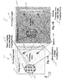
- Figure 1A shows one example of a die interconnect 100 on a chip 102.
- Figure 1B shows one example of the die interconnect 100 on a substrate 120.
- the die interconnect 100 can be first fabricated on either the chip 102 or the substrate 120 before the chip 102 and substrate 120 are connected together by the die interconnect 100 thereby forming a package.
- Chip and die are used interchangeably in this specification and refer to a circuit element or a collection of circuit elements.
- the die interconnect 100 includes the chip 102 having a chip area 104, or alternately the substrate 120 having a substrate area 122.
- the chip and substrate areas 104, 122 include an overhang area 106, a rigid coupling area 110 and a flexible coupling area 116.
- the rigid coupling area 110 includes a set of rigid coupling points 112, located on one side of the overhang area 106.
- the flexible coupling area 116 includes a set of flexible coupling points 306, located on a side of the overhang area 106 opposite to the a rigid coupling area 110.
- the rigid coupling points 112 are electrical coupling points and the flexible coupling points 306 are mechanical coupling points.
- the rigid coupling points 112 are formed from anisotropic conductive adhesive (ACA) glue.
- ACA glue anisotropic conductive adhesive
- the ACA glue shrinks when cured and silver particles within the ACA create an electrical contact between the two metal surfaces.
- ACA glue does not conduct in the x-y axis directions.
- ACA glue may be deposited on the chip 102 or substrate 120 using either a lamination, dispense or screen printing process.
- the ACA glue is replaced by rigid solder bumps, copper (Cu) stud-bumps or a wire bond.
- Use of ACA glue however enables a pitch (i.e. distance) between the electrical contacts to be smaller than solder connections would permit.
- the ACA glue can also be replaced by a NCA (Non Conductive Adhesive) along with Cu stud bumps having an Sn cap that allows soldering on to the substrate. Pitch using the NCA-type interconnect may be low as well.
- the ACA glue can be applied in the shape of an anisotropic conductive paste (ACP) or in the shape of anisotropic conductive foil (ACF)
- the flexible coupling points in the flexible coupling area 116 are formed from a soft flexible, non-conductive, glue which flexes along x-y-z axes to avoid stress build-up. Glues from the silicone family of glues that permit in plane movement can be used in this flexible coupling area.
- a set of spacers 118 are located within either the overhang area 106 or the flexible coupling area 116.
- the spacers 118 prevent tilting during the package assembly process and help ensure a relatively constant gap between the Si chip 102 and the substrate 120.
- These spacers 118 can be either filler particles in a soft glue or additional bumps similar to the ones which form the rigid or flexible coupling points.
- the spacer bumps 118 are fixed to the chip 102 but not to the substrate 120 and thus can slide over the substrate 120 without adding stress to the chip 102.
- the rigid coupling area 110 is within an outer boundary 114 and the flexible coupling area 116 and overhang area 106 are outside of the outer boundary 114.
- the outer boundary 114 encloses up to 50% of the chip area 104.
- the chip or substrate area 104, 122 is defined by a x-axis length and a y-axis width
- the overhang area 106 has an x-axis overhang length 108 which is at least 50% of the chip or substrate area's 104 or 122 x-axis length.
- the % overlap can range from 1% to 99%.
- the substrate 120 could be a second chip, a circuit board or glass.
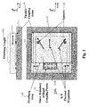
- Figure 2 is one example of a die interconnect 100 between a chip 102 and a substrate 120.
- the chip 102 has already been connected to the substrate 120 using the die interconnect 100 thereby forming a package.
- the chip 102 is transparent so that the die interconnect 100 can be seen.
- Fig. 2 shows an example of how the chip 102 can be fixed to a substrate 120 on only a small area. As such the stress build up between the Si chip 102 and substrate 120 is minimized.
- the chip 102 is coupled to the substrate 120 with the set of rigid 112 and flexible coupling points in the flexible coupling area 116.
- the flexible coupling area 116 can be on a side of the overhang area 106 opposite to 204 the rigid coupling points 112.
- the flexible coupling area 116 can be adjacent to 206 the rigid coupling points 112 and on a same side of the overhang area 106 as the rigid coupling points 112.
- both the conductive ACA glue and the non-conductive silicone glue are applied to the chip 102 or substrate 120.
- the chip 102 is then placed in position over the substrate 120 and the two are pressed together to mount the chip 102 to the substrate 120.
- the conductive ACA glue is applied to the chip 102 or substrate 120, the chip 102 and substrate 120 are connected, the ACA glue is cured and then a fillet of silicone glue is placed around the outside edge of the chip 102 and onto the substrate 120 below and the silicone is cured.
- Fig. 2 also shows an example of how the optional spacer bump 118 keeps the chip 102 and substrate 120 at a relatively constant distance.
- an additional fillet of the flexible glue can also be applied around the or on several points to further fix the chip.
- the substrate array can be cut into individual packages using chip singulation, punching or other separation technique.
- a cap could be placed over the chip (e.g. Si chip) for mechanical protection.
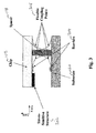
- Figure 3 is one example of a flexible coupling point 306 within a die interconnect 100.
- the spacer 118 is included in the flexible coupling area 116 to prevent tilting of the chip.
- the spacer 118 is surrounded with a flexible glue such as silicone. As can be seen, the glue can flow out toward a stress-sensitive structure 302 located in the overhang area 106.
- a set of barriers 304 are affixed to both the chip 102 and the substrate 120.
- the barrier 304 is inserted between a portion of the chip or substrate areas 104, 122 and either the rigid coupling area 110 or the flexible coupling area 116.
- the barrier 304 can be formed from: a dam, a reservoir, a topography, a mask, a copper trace with a barrier mask, a polyimide coating, or a passivation layer.
- the stress-sensitive structure 302 can include a variety of structures which may be sensitive to stress, such as: a mechanical device, an electrical device, a sensor (e.g. pressure or otherwise), a functional electrical block, an electrical component (e.g. a resistor, a capacitor, etc.) and/or a functional parameter.
- FIG 4 is one example of a rigid coupling point 112 within a die interconnect.
- the rigid coupling point 112 includes an anisotropic conductive adhesive (ACA) 402, a conductive bump 404, and a copper (Cu) trace 406.
- the conductive bump 404 electrically coupled to the chip 102 and the copper trace 406 is mechanically coupled to the substrate 120.
- the ACA glue 402 flows between the conductive bump 404 and the copper trace 406 forming an electrical coupling after cure.
- the copper trace 406 includes a barrier 407 which can be copper or another substance. In Figure 4 the barrier 407 is also formed from the copper trace 406. The barrier 407 helps prevent flow-out of the ACA glue 402 before the glue is cured.
- ACA 402 glue can be applied in the shape of an anisotropic conductive paste (ACP) or in the shape of anisotropic conductive foil (ACF).
- ACP anisotropic conductive paste
- ACF anisotropic conductive foil
- Figure 5 lists one example of a method 500 for fabricating a die interconnect.
- the method 500 begins in block 502, by fabricating a rigid coupler area, having a set of rigid coupler points, within a chip having a chip area.
- a rigid coupler area having a set of rigid coupler points, within a chip having a chip area.
- fabricating a flexible coupler area having a set of flexible coupler points, within the chip area abutted to a side of the overhang area opposite to the rigid coupler area.
- the rigid coupler points can, in one example, be fabricated with conductive bumps, and the flexible coupler points can be fabricated with silicone.
- a substrate is coupled to the chip at both the rigid coupler points and the flexible coupler points.
- the die interconnect may comprise:
- the die interconnect may comprise:
- Example embodiments discussed in this specification can be implemented in whole or in part within a variety of electronic, and non-electronic devices, apparatus, systems and structures.
Landscapes
- Engineering & Computer Science (AREA)
- Microelectronics & Electronic Packaging (AREA)
- Computer Hardware Design (AREA)
- Wire Bonding (AREA)
- Manufacturing & Machinery (AREA)
- Electric Connection Of Electric Components To Printed Circuits (AREA)
Abstract
fabricating a rigid coupler area, having a set of rigid coupler points, within a chip having a chip area; defining an overhang area within the chip area and abutted to the rigid coupler area; and
fabricating a flexible coupler area, having a set of flexible coupler points, within the chip area abutted to a side of the overhang area opposite to the rigid coupler area.
Description
- This specification relates generally to device attachments and in one example to a die interconnect.
-
-
Figure 1A shows one example of a die interconnect on a chip. -
Figure 1 B shows one example of a die interconnect on a substrate. -
Figure 2 shows one example of a die interconnect between a chip and a substrate. -
Figure 3 shows one example of a flexible coupling point within a die interconnect. -
Figure 4 shows one example of a rigid coupling point within a die interconnect. -
Figure 5 lists one example of a method for fabricating a die interconnect. - While the disclosure is amenable to various modifications and alternative forms, specifics thereof have been shown by way of example in the drawings and will be described in detail. It should be understood, however, that other embodiments, beyond the particular embodiments described, are possible as well. All modifications, equivalents, and alternative embodiments falling within the spirit and scope of the appended claims are covered as well.
- Semiconductor devices whose input/output (IO) pins are spread out over the chip surface can result in a very stiff connection between a chip and substrate such that thermal mismatch between chip and substrate results in chip stresses.
- Semiconductor devices include sensors (e.g. pressure sensors). Such sensors, dependent on the design, are sensitive to stress on an Si die (e.g. a silicon chip) which will affect the sensor's sensitivity and accuracy.
- Stress on Si sensor chip can be generated when materials with different thermomechanical properties are connected together. This stress is an effect of a difference in coefficients of thermal expansion (CTE) and in combination with the modulus of the material, leads to stresses. Temperature changes in this case lead to a variation in stress. Also Humidity variations can lead to stress variations especially when organic materials are used. The chip itself can generally cope with these stresses but the sensor which is processed on the chip surface will be affected by minimal amounts of stress change. Also when organic materials or metals are used variation in stress (e.g. relaxation) over time can happen due to creep effects of these materials. As some Si sensors are used for absolute measurements stress variation over time could create inaccurate sensor signals.
- Mounting the Si chip on a substrate with similar coefficients of thermal expansion may not always result in the best or most economical solution. Other alternatives using wire-bonds and flexible glues in pre-molded or cavity packages can lead to increase in size and cost.
- In one example embodiment discussed in more detail below, chip stress is minimized by fixing the chip on one relatively small area, using flip chip interconnect, thereby letting the chip freely expand in all directions. Flip chip in general is a very stiff construction not allowing for stress relief but by using a small area with fine pitch interconnections between chip and substrate the stress is minimal and localized in that small area. The rest of the chip remains stress free. By grouping all interconnects on a small area, the mismatch in thermal expansion is reduced and thus the absolute stress is reduced (small distance), so that the remainder of the chip remains free from stress including a sensor area.
- With the contact between the Si chip and the carrier substrate minimized, the majority of the chip is free to expand and contract due to temperature variations without building up stress on not contacted areas. The area which is in contact with the carrier substrate is kept minimal. This set of rigid coupling points can be located at various chip locations and be arranged in different patterns. In such embodiments, the stress build up increases with the dimension of the contact. The smaller this contact the smaller the stress. An area which is sensitive for the stress can be on a different location on the Si chip.
- Details of the present claimed device/service are now discussed.
-
Figure 1A shows one example of adie interconnect 100 on achip 102.Figure 1B shows one example of the dieinterconnect 100 on asubstrate 120. Thus thedie interconnect 100 can be first fabricated on either thechip 102 or thesubstrate 120 before thechip 102 andsubstrate 120 are connected together by thedie interconnect 100 thereby forming a package. Chip and die are used interchangeably in this specification and refer to a circuit element or a collection of circuit elements. - The die
interconnect 100 includes thechip 102 having achip area 104, or alternately thesubstrate 120 having asubstrate area 122. The chip andsubstrate areas overhang area 106, arigid coupling area 110 and aflexible coupling area 116. Therigid coupling area 110 includes a set ofrigid coupling points 112, located on one side of theoverhang area 106. Theflexible coupling area 116, includes a set offlexible coupling points 306, located on a side of theoverhang area 106 opposite to the arigid coupling area 110. In one example, therigid coupling points 112 are electrical coupling points and theflexible coupling points 306 are mechanical coupling points. - In an example embodiment, the
rigid coupling points 112 are formed from anisotropic conductive adhesive (ACA) glue. When placed between two closely spaced metal surfaces, the ACA glue shrinks when cured and silver particles within the ACA create an electrical contact between the two metal surfaces. ACA glue does not conduct in the x-y axis directions. ACA glue may be deposited on thechip 102 orsubstrate 120 using either a lamination, dispense or screen printing process. - In another example embodiment, the ACA glue is replaced by rigid solder bumps, copper (Cu) stud-bumps or a wire bond. Use of ACA glue however enables a pitch (i.e. distance) between the electrical contacts to be smaller than solder connections would permit. The ACA glue can also be replaced by a NCA (Non Conductive Adhesive) along with Cu stud bumps having an Sn cap that allows soldering on to the substrate. Pitch using the NCA-type interconnect may be low as well. In other examples, the ACA glue can be applied in the shape of an anisotropic conductive paste (ACP) or in the shape of anisotropic conductive foil (ACF)
- The flexible coupling points in the
flexible coupling area 116, in one example, are formed from a soft flexible, non-conductive, glue which flexes along x-y-z axes to avoid stress build-up. Glues from the silicone family of glues that permit in plane movement can be used in this flexible coupling area. - In an example embodiment, a set of
spacers 118 are located within either theoverhang area 106 or theflexible coupling area 116. Thespacers 118 prevent tilting during the package assembly process and help ensure a relatively constant gap between theSi chip 102 and thesubstrate 120. Thesespacers 118 can be either filler particles in a soft glue or additional bumps similar to the ones which form the rigid or flexible coupling points. In one example, thespacer bumps 118 are fixed to thechip 102 but not to thesubstrate 120 and thus can slide over thesubstrate 120 without adding stress to thechip 102. - The
rigid coupling area 110 is within anouter boundary 114 and theflexible coupling area 116 andoverhang area 106 are outside of theouter boundary 114. In one example, theouter boundary 114 encloses up to 50% of thechip area 104. In another example, the chip orsubstrate area overhang area 106 has anx-axis overhang length 108 which is at least 50% of the chip or substrate area's 104 or 122 x-axis length. However in other examples, the % overlap can range from 1% to 99%. - In different example embodiments, the
substrate 120 could be a second chip, a circuit board or glass. -
Figure 2 is one example of adie interconnect 100 between achip 102 and asubstrate 120. In this example thechip 102 has already been connected to thesubstrate 120 using thedie interconnect 100 thereby forming a package. For clarity, in the x-y view of the package ofFig. 2 thechip 102 is transparent so that thedie interconnect 100 can be seen.Fig. 2 shows an example of how thechip 102 can be fixed to asubstrate 120 on only a small area. As such the stress build up between theSi chip 102 andsubstrate 120 is minimized. - The
chip 102 is coupled to thesubstrate 120 with the set of rigid 112 and flexible coupling points in theflexible coupling area 116. As shown inFigure 2 , theflexible coupling area 116 can be on a side of theoverhang area 106 opposite to 204 the rigid coupling points 112. Alternatively, theflexible coupling area 116 can be adjacent to 206 therigid coupling points 112 and on a same side of theoverhang area 106 as the rigid coupling points 112. Several options for connecting thechip 102 to thesubstrate 120 are possible. - In one example both the conductive ACA glue and the non-conductive silicone glue are applied to the
chip 102 orsubstrate 120. Thechip 102 is then placed in position over thesubstrate 120 and the two are pressed together to mount thechip 102 to thesubstrate 120. - In another example, the conductive ACA glue is applied to the
chip 102 orsubstrate 120, thechip 102 andsubstrate 120 are connected, the ACA glue is cured and then a fillet of silicone glue is placed around the outside edge of thechip 102 and onto thesubstrate 120 below and the silicone is cured. -
Fig. 2 also shows an example of how theoptional spacer bump 118 keeps thechip 102 andsubstrate 120 at a relatively constant distance. After the chip and substrate are coupled, an additional fillet of the flexible glue can also be applied around the or on several points to further fix the chip. After curing the substrate array can be cut into individual packages using chip singulation, punching or other separation technique. Optionally a cap could be placed over the chip (e.g. Si chip) for mechanical protection. - With the
rigid coupling points 112 localized on thechip 102 x-ythermal expansion 202 can more easily be accommodated resulting inless chip 102 stress. -
Figure 3 is one example of aflexible coupling point 306 within adie interconnect 100. In this example thespacer 118 is included in theflexible coupling area 116 to prevent tilting of the chip. Thespacer 118 is surrounded with a flexible glue such as silicone. As can be seen, the glue can flow out toward a stress-sensitive structure 302 located in theoverhang area 106. - Since glue contact with the stress-
sensitive structure 302 might affect proper functioning of thestructure 302, a set ofbarriers 304 are affixed to both thechip 102 and thesubstrate 120. In another example, thebarrier 304 is inserted between a portion of the chip orsubstrate areas rigid coupling area 110 or theflexible coupling area 116. - In various example embodiments, the
barrier 304 can be formed from: a dam, a reservoir, a topography, a mask, a copper trace with a barrier mask, a polyimide coating, or a passivation layer. - Note that the stress-
sensitive structure 302 can include a variety of structures which may be sensitive to stress, such as: a mechanical device, an electrical device, a sensor (e.g. pressure or otherwise), a functional electrical block, an electrical component (e.g. a resistor, a capacitor, etc.) and/or a functional parameter. -
Figure 4 is one example of arigid coupling point 112 within a die interconnect. Therigid coupling point 112 includes an anisotropic conductive adhesive (ACA) 402, aconductive bump 404, and a copper (Cu)trace 406. Theconductive bump 404 electrically coupled to thechip 102 and thecopper trace 406 is mechanically coupled to thesubstrate 120. TheACA glue 402 flows between theconductive bump 404 and thecopper trace 406 forming an electrical coupling after cure. Thecopper trace 406 includes abarrier 407 which can be copper or another substance. InFigure 4 thebarrier 407 is also formed from thecopper trace 406. Thebarrier 407 helps prevent flow-out of theACA glue 402 before the glue is cured. Other barriers to theACA 402 glue include: amask barrier 408, atopography barrier 410, and areservoir barrier 412. As mentioned above, the ACA glue can be applied in the shape of an anisotropic conductive paste (ACP) or in the shape of anisotropic conductive foil (ACF). -
Figure 5 lists one example of a method 500 for fabricating a die interconnect. The method 500 begins inblock 502, by fabricating a rigid coupler area, having a set of rigid coupler points, within a chip having a chip area. Inblock 504, defining an overhang area within the chip area and abutted to the rigid coupler area. Then inblock 506, fabricating a flexible coupler area, having a set of flexible coupler points, within the chip area abutted to a side of the overhang area opposite to the rigid coupler area. Inblock 508, the rigid coupler points can, in one example, be fabricated with conductive bumps, and the flexible coupler points can be fabricated with silicone. Then inblock 510, a substrate is coupled to the chip at both the rigid coupler points and the flexible coupler points. - In an example embodiment the die interconnect, may comprise:
- a chip having a chip area defined by a x-axis length and a y-axis width, wherein the chip area includes: an overhang area having an x-axis overhang length which is at least 50% of the chip area x-axis length; and a rigid coupling area, having a set of rigid coupling points, located on one side of the overhang area.
- In an example embodiment the die interconnect, may comprise:
- a chip having a chip area, wherein the chip area includes: an overhang area; a rigid coupling area, having a set of rigid coupling points, located on one side of the overhang area; and a flexible coupling area, having a set of flexible coupling points, located adjacent to the rigid coupling area and on a same side of the overhang area as the rigid coupling area.
- The blocks comprising the flowcharts in the above Figures can be executed in any order, unless a specific order is explicitly stated. Also, those skilled in the art will recognize that while one example method embodiment is now discussed, the material in this specification can be combined in a variety of ways to yield other examples as well. The method next discussed is to be understood within a context provided by this and other portions of this detailed description.
- Example embodiments discussed in this specification can be implemented in whole or in part within a variety of electronic, and non-electronic devices, apparatus, systems and structures.
- In this specification, example embodiments have been presented in terms of a selected set of details. However, a person of ordinary skill in the art would understand that many other example embodiments may be practiced which include a different selected set of these details. It is intended that the following claims cover all possible example embodiments.
Claims (15)
- A die interconnect, comprising:a chip having a chip area, wherein the chip area includes:an overhang area;a rigid coupling area, having a set of rigid coupling points, located on one side of the overhang area; anda flexible coupling area, having a set of flexible coupling points,located on a side of the overhang area opposite to the rigid coupling area.
- The die interconnect of claim 1, wherein:the rigid coupling points are electrical coupling points; andthe flexible coupling points are mechanical coupling points.
- The die interconnect of claim 1, further comprising:a set of spacers located within either the overhang area or the flexible coupling area.
- The die interconnect of claim 1, wherein:the rigid coupling area is within an outer boundary; andthe flexible coupling area and overhang area are outside of the outer boundary.
- The die interconnect of claim 4, wherein the outer boundary encloses up to 50% of the chip area.
- The die interconnect of claim 1, wherein the chip is coupled to a substrate with the set of rigid and flexible coupling points.
- The die interconnect of claim 6, wherein the substrate includes at least one from a group consisting of: a second chip: a circuit board, ceramic substrate and glass.
- The die interconnect of claim 1:wherein the chip includes a stress-sensitive structure located in the overhang area; andwherein the stress-sensitive structure includes at least one from a group consisting of: a mechanical device, an electrical device, a sensor, a functional electrical block, an electrical component and a functional parameter.
- The die interconnect of claim 1, wherein the rigid coupling points include at least one from a group consisting of: an anisotropic conductive adhesive and a conductive bump.
- The die interconnect of claim 1, wherein the flexible coupling points include a silicone glue.
- The die interconnect of claim 1, further comprising:a barrier between a portion of the chip area and either the rigid coupling area or the flexible coupling area.
- The die interconnect of claim 1, wherein the barrier is at least one from a group consisting of: a dam, a reservoir, a topography, a mask, and PI.
- A method for fabricating a die interconnect, comprising:fabricating a rigid coupler area, having a set of rigid coupler points, within a chip having a chip area;defining an overhang area within the chip area and abutted to the rigid coupler area; andfabricating a flexible coupler area, having a set of flexible coupler points,
within the chip area abutted to a side of the overhang area opposite to the rigid coupler area. - The method of claim 13, further comprising:coupling a substrate to the chip at both the rigid coupler points and the flexible coupler points.
- The method of claim 13, further comprising:fabricating the rigid coupler points with at least one from a group consisting of:anisotropic conductive adhesive, anisotropic conductive film and anisotropic conductive paste; andfabricating the flexible coupler points with silicone.
Applications Claiming Priority (1)
| Application Number | Priority Date | Filing Date | Title |
|---|---|---|---|
| US14/229,717 US9385099B2 (en) | 2014-03-28 | 2014-03-28 | Die interconnect |
Publications (2)
| Publication Number | Publication Date |
|---|---|
| EP2923999A2 true EP2923999A2 (en) | 2015-09-30 |
| EP2923999A3 EP2923999A3 (en) | 2016-01-13 |
Family
ID=52686220
Family Applications (1)
| Application Number | Title | Priority Date | Filing Date |
|---|---|---|---|
| EP15159573.3A Withdrawn EP2923999A3 (en) | 2014-03-28 | 2015-03-18 | Die interconnect |
Country Status (3)
| Country | Link |
|---|---|
| US (1) | US9385099B2 (en) |
| EP (1) | EP2923999A3 (en) |
| CN (1) | CN104952842B (en) |
Families Citing this family (3)
| Publication number | Priority date | Publication date | Assignee | Title |
|---|---|---|---|---|
| KR20160149905A (en) * | 2015-06-19 | 2016-12-28 | 에스케이하이닉스 주식회사 | Semiconductor package with sliding interconnection structure |
| US11670521B2 (en) * | 2019-12-19 | 2023-06-06 | Utac Headquarters PTE. Ltd | Reliable semiconductor packages for sensor chips |
| TWI736093B (en) | 2019-12-31 | 2021-08-11 | 財團法人工業技術研究院 | Package structure |
Family Cites Families (10)
| Publication number | Priority date | Publication date | Assignee | Title |
|---|---|---|---|---|
| US20020146919A1 (en) | 2000-12-29 | 2002-10-10 | Cohn Michael B. | Micromachined springs for strain relieved electrical connections to IC chips |
| DE10135393B4 (en) | 2001-07-25 | 2004-02-05 | Infineon Technologies Ag | Electronic component, manufacturing method, and method for establishing an electrical connection between the component and a circuit board |
| JP3971674B2 (en) * | 2002-07-10 | 2007-09-05 | 富士通株式会社 | Contact-type sensor built-in semiconductor device and manufacturing method thereof |
| JP4196901B2 (en) * | 2004-08-11 | 2008-12-17 | ソニー株式会社 | Electronic circuit equipment |
| US7221053B2 (en) | 2005-03-21 | 2007-05-22 | Infineon Technologies Ag | Integrated device and electronic system |
| US20080290430A1 (en) * | 2007-05-25 | 2008-11-27 | Freescale Semiconductor, Inc. | Stress-Isolated MEMS Device and Method Therefor |
| DE102010012042B4 (en) | 2010-03-19 | 2025-02-06 | Tdk Corporation | Component with a chip in a cavity and a stress-reduced attachment |
| US8469607B2 (en) * | 2011-05-09 | 2013-06-25 | Hewlett-Packard Development Company, L.P. | Opto-electronics with compliant electrical contacts |
| US20150049443A1 (en) * | 2013-08-13 | 2015-02-19 | Infineon Technologies Ag | Chip arrangement |
| TWI524998B (en) * | 2013-09-25 | 2016-03-11 | 友達光電股份有限公司 | Method for bonding and separating substrates |
-
2014
- 2014-03-28 US US14/229,717 patent/US9385099B2/en not_active Expired - Fee Related
-
2015
- 2015-03-18 EP EP15159573.3A patent/EP2923999A3/en not_active Withdrawn
- 2015-03-30 CN CN201510145577.6A patent/CN104952842B/en not_active Expired - Fee Related
Non-Patent Citations (1)
| Title |
|---|
| None |
Also Published As
| Publication number | Publication date |
|---|---|
| EP2923999A3 (en) | 2016-01-13 |
| US9385099B2 (en) | 2016-07-05 |
| US20150279803A1 (en) | 2015-10-01 |
| CN104952842A (en) | 2015-09-30 |
| CN104952842B (en) | 2018-08-31 |
Similar Documents
| Publication | Publication Date | Title |
|---|---|---|
| EP3465758B1 (en) | Image sensor semiconductor packages and related methods | |
| KR102938134B1 (en) | Semiconductor package and method of manufacturing the same | |
| US8890304B2 (en) | Fan-out microelectronic unit WLP having interconnects comprising a matrix of a high melting point, a low melting point and a polymer material | |
| TWI763666B (en) | Connecting electronic components to substrates | |
| CN105280567B (en) | Semiconductor package assembly and a manufacturing method thereof | |
| CN100533712C (en) | Photoelectric element chip and manufacturing method thereof | |
| EP3007102B1 (en) | Semiconductor device and method for manufacturing semiconductor device | |
| US20110115036A1 (en) | Device packages and methods of fabricating the same | |
| CN111799283A (en) | Controllable gap height for image sensor packaging | |
| CN109891430B (en) | Fingerprint sensor module and method for manufacturing a fingerprint sensor module | |
| CN110402492B (en) | Flexible conductive adhesive | |
| EP2897163B1 (en) | Semiconductor device and method of manufacturing a semiconductor device | |
| US11492250B2 (en) | Electronic device and method for manufacturing an electronic device | |
| US9385099B2 (en) | Die interconnect | |
| CN101308802A (en) | Sensing type semiconductor device and manufacturing method thereof | |
| US11101189B2 (en) | Semiconductor device package and method of manufacturing the same | |
| KR20100031775A (en) | Electronic component | |
| CN112352305A (en) | Chip packaging structure and chip packaging method | |
| WO2016051726A1 (en) | Hall sensor manufacturing method, hall sensor, and lens module | |
| KR20100031766A (en) | Electronic component | |
| EP2884242B1 (en) | Sensor Package And Manufacturing Method | |
| US7038321B1 (en) | Method of attaching a flip chip device and circuit assembly formed thereby | |
| CN104979302A (en) | Chip package and manufacturing method thereof | |
| JP5230578B2 (en) | Electronic component mounting board | |
| US20220216255A1 (en) | Image sensor package having inner and outer joint members |
Legal Events
| Date | Code | Title | Description |
|---|---|---|---|
| PUAI | Public reference made under article 153(3) epc to a published international application that has entered the european phase |
Free format text: ORIGINAL CODE: 0009012 |
|
| AK | Designated contracting states |
Kind code of ref document: A2 Designated state(s): AL AT BE BG CH CY CZ DE DK EE ES FI FR GB GR HR HU IE IS IT LI LT LU LV MC MK MT NL NO PL PT RO RS SE SI SK SM TR |
|
| AX | Request for extension of the european patent |
Extension state: BA ME |
|
| PUAL | Search report despatched |
Free format text: ORIGINAL CODE: 0009013 |
|
| AK | Designated contracting states |
Kind code of ref document: A3 Designated state(s): AL AT BE BG CH CY CZ DE DK EE ES FI FR GB GR HR HU IE IS IT LI LT LU LV MC MK MT NL NO PL PT RO RS SE SI SK SM TR |
|
| AX | Request for extension of the european patent |
Extension state: BA ME |
|
| RIC1 | Information provided on ipc code assigned before grant |
Ipc: B81B 7/00 20060101AFI20151208BHEP |
|
| RIC1 | Information provided on ipc code assigned before grant |
Ipc: B81B 7/00 20060101AFI20160308BHEP |
|
| 17P | Request for examination filed |
Effective date: 20160713 |
|
| RBV | Designated contracting states (corrected) |
Designated state(s): AL AT BE BG CH CY CZ DE DK EE ES FI FR GB GR HR HU IE IS IT LI LT LU LV MC MK MT NL NO PL PT RO RS SE SI SK SM TR |
|
| STAA | Information on the status of an ep patent application or granted ep patent |
Free format text: STATUS: THE APPLICATION IS DEEMED TO BE WITHDRAWN |
|
| 18D | Application deemed to be withdrawn |
Effective date: 20160714 |