EP2920844B1 - Method and apparatus for a tunable antenna - Google Patents
Method and apparatus for a tunable antenna Download PDFInfo
- Publication number
- EP2920844B1 EP2920844B1 EP13868648.0A EP13868648A EP2920844B1 EP 2920844 B1 EP2920844 B1 EP 2920844B1 EP 13868648 A EP13868648 A EP 13868648A EP 2920844 B1 EP2920844 B1 EP 2920844B1
- Authority
- EP
- European Patent Office
- Prior art keywords
- antenna
- tunable
- ghz
- operating frequency
- capacitance
- Prior art date
- Legal status (The legal status is an assumption and is not a legal conclusion. Google has not performed a legal analysis and makes no representation as to the accuracy of the status listed.)
- Active
Links
Images






Classifications
-
- H—ELECTRICITY
- H04—ELECTRIC COMMUNICATION TECHNIQUE
- H04B—TRANSMISSION
- H04B1/00—Details of transmission systems, not covered by a single one of groups H04B3/00 - H04B13/00; Details of transmission systems not characterised by the medium used for transmission
- H04B1/38—Transceivers, i.e. devices in which transmitter and receiver form a structural unit and in which at least one part is used for functions of transmitting and receiving
- H04B1/40—Circuits
-
- H—ELECTRICITY
- H01—ELECTRIC ELEMENTS
- H01Q—ANTENNAS, i.e. RADIO AERIALS
- H01Q5/00—Arrangements for simultaneous operation of antennas on two or more different wavebands, e.g. dual-band or multi-band arrangements
- H01Q5/30—Arrangements for providing operation on different wavebands
- H01Q5/378—Combination of fed elements with parasitic elements
- H01Q5/392—Combination of fed elements with parasitic elements the parasitic elements having dual-band or multi-band characteristics
-
- H—ELECTRICITY
- H01—ELECTRIC ELEMENTS
- H01Q—ANTENNAS, i.e. RADIO AERIALS
- H01Q9/00—Electrically-short antennas having dimensions not more than twice the operating wavelength and consisting of conductive active radiating elements
- H01Q9/04—Resonant antennas
- H01Q9/06—Details
-
- H—ELECTRICITY
- H01—ELECTRIC ELEMENTS
- H01Q—ANTENNAS, i.e. RADIO AERIALS
- H01Q9/00—Electrically-short antennas having dimensions not more than twice the operating wavelength and consisting of conductive active radiating elements
- H01Q9/04—Resonant antennas
- H01Q9/30—Resonant antennas with feed to end of elongated active element, e.g. unipole
- H01Q9/42—Resonant antennas with feed to end of elongated active element, e.g. unipole with folded element, the folded parts being spaced apart a small fraction of the operating wavelength
-
- H—ELECTRICITY
- H01—ELECTRIC ELEMENTS
- H01Q—ANTENNAS, i.e. RADIO AERIALS
- H01Q1/00—Details of, or arrangements associated with, antennas
- H01Q1/12—Supports; Mounting means
- H01Q1/22—Supports; Mounting means by structural association with other equipment or articles
- H01Q1/24—Supports; Mounting means by structural association with other equipment or articles with receiving set
- H01Q1/241—Supports; Mounting means by structural association with other equipment or articles with receiving set used in mobile communications, e.g. GSM
- H01Q1/242—Supports; Mounting means by structural association with other equipment or articles with receiving set used in mobile communications, e.g. GSM specially adapted for hand-held use
- H01Q1/243—Supports; Mounting means by structural association with other equipment or articles with receiving set used in mobile communications, e.g. GSM specially adapted for hand-held use with built-in antennas
Definitions
- Wireless communication technologies and services continue to proliferate leading to new voice and data services, carrier aggregation, and new demands on roaming to name a few.
- technologies advance and user demand for services increases, wireless communication devices need to support an increasing number of operating frequency bands to support the technologies and services.
- wireless communication devices are getting smaller. For example, mobile phones are becoming increasingly thinner, and as a result there may be less volume available for antenna structures and systems, as well as less space for the coexistence of electromechanical components around the antenna.
- WO 2011/059088A1 refers to an antenna device comprising an antenna element disposed on a mounting board separate from a main circuit board, a coupling means disposed on the mounting board such that it is electromagnetically coupled to the antenna element, and a frequency-adjusting means disposed on the mounting board such that it is connected to the coupling means, the antenna element comprising first and second strip-shaped antenna elements integrally connected for sharing a feeding point, the second antenna element being shorter than the first antenna element; the coupling means being formed on a dielectric chip attached to the mounting board, and having a coupling electrode electromagnetically coupled to part of the first antenna element.
- the frequency-adjusting means comprises a parallel resonance circuit comprising a variable capacitance circuit and a first inductance element, and a second inductance element series-connected to the parallel resonance circuit.
- US 2003/0210203A1 refers to an adaptive antenna system having a counterpoise conductor contained within a housing of a communication device and located distally from such surfaces of the housing that can be held by or placed in proximity to a user or external objects which detune the counterpoise.
- a tuning circuit is coupled between the counterpoise conductor and a ground. The tuning circuit is operable to adapt the resonant frequency of the counterpoise conductor to divert operational RF currents away from the ground located in proximity the user or external objects and onto the counterpoise conductor.
- US 2006/0252391A1 refers to an apparatus, system and method optimizing antenna performance using tunable parasitic elements by changing antenna characteristics based on signal quality parameters of electromagnetic signals exchanged through the antenna.
- the tunable parasitic elements are responsive to control signals to modify current flowing through a counterpoise of the antenna.
- transmission characteristics are optimized by increasing the transmission gain in the direction of the receiving base station.
- Signal quality parameters measured at the antenna are used to change reception characteristics by minimizing reception gain in the direction of a jamming transmitter.
- US 2009/0224991A1 refers to an antenna comprising an IMD element, and one or more parasitic and active tuning elements.
- the IMD element when used in combination with the active tuning and parasitic elements, allows antenna operation at multiple resonant frequencies.
- the direction of antenna radiation pattern may be arbitrarily rotated in accordance with the parasitic and active tuning elements.
- an apparatus comprising:
- the capacitance of the tunable load is tunable in the range of about 1.8 picofarads (pF) to about 5 picofarads, wherein if the tunable load is about 1.8 pF an operating frequency low band is about 0.69 gigahertz (GHz) to about 0.75 GHz and an operating frequency high band of is about 1.66 GHz to about 2.26 GHz, wherein if the tunable load is about 2.5 pF the operating frequency low band is about 0.81 GHz to about 0.89 GHz and the operating frequency high band is about 1.74 GHz to 2.27 GHz, and wherein if the tunable load is about 1.8 pF the operating frequency low band is about 0.87 GHz to about 0.96 GHz and the operating frequency high band is about 1.42 GHz to about 1.59 GHz.
- pF picofarads
- the apparatus is a wireless communication device, wherein the apparatus further comprises: a processor coupled to the tunable load and configured to:
- the apparatus further comprises:
- the apparatus further comprises a proximity sensor coupled to the processor, wherein the processor is further configured to receive a proximity sensor measurement and take the proximity sensor measurement into account in selecting the first operating frequency band.
- a tunable antenna For example, operating frequency bands of the tunable antenna may be adjusted by varying a load of a parasitic arm electromagnetically coupled to an antenna. Also disclosed herein is a method of tuning an antenna. For example, the antenna may be tuned by adjusting a load of a parasitic arm electromagnetically coupled to the antenna.
- the tunable antenna apparatuses and methods may be suitable for implementation in compact wireless communication devices.
- FIG. 1 is a schematic diagram of an embodiment of a tunable antenna.
- the tunable antenna 100 comprises an antenna 102, a feed line 110, a parasitic arm 104, and a tunable load 106 configured as shown in FIG. 1 .
- the antenna 102 may be coupled to a transceiver (not shown) via the antenna feed line 110.
- the parasitic arm 104 is located in close enough proximity with the antenna 102 to be coupled to the antenna 102 electromagnetically. However, as shown there may be no direct connection between the parasitic arm 104 and the antenna 102. Further, the parasitic arm 104 may be coupled to a tunable load 106.
- the tunable load 106 may be connected to ground as shown or may be maintained at a substantially constant non-zero voltage level.
- the tunable load may have a variable or tunable impedance (i.e., combination of resistance, capacitance, and/or inductance).
- a fixed or non-tunable inductor may be placed in series with a tunable capacitor to provide a variable impedance.
- the tunable capacitor may be implemented as a radio frequency (RF) switching device, a varactor, a single pole multi throw ("SPxT") switch, a digital tunable capacitor (“DTC”), or a micro-electromechanical system (“MEMS”) capacitor array.
- RF radio frequency
- SPxT single pole multi throw
- DTC digital tunable capacitor
- MEMS micro-electromechanical system
- the antenna 102 may be any antenna type that allows for variable and continuous tuning by adjusting the tunable load 106.
- antenna types include but are not limited to inverted-F antennas ("IFAs"), loop antennas, slot antennas, or folded inverted conformal antennas (FICAs).
- IFAs inverted-F antennas
- FICAs folded inverted conformal antennas
- the parasitic arm 104 and the antenna 102 are coupled to each other electromagnetically.
- the parasitic arm 104 may be tuned separately from the antenna by varying the tunable load 106 coupled to the parasitic arm. Varying the tunable load affects the operating frequency band of the antenna 102, thus adjusting at least one operating parameter of the antenna 102 without the need to add capacitance directly to the antenna.
- Continuous tuning of the antenna 102 may be possible if tuning capabilities of the tunable load 106 are continuous. For example, because both a DTC and a MEMS capacitor array may be continuously tunable, the selection of either of these tunable loads may result in a continuously tunable antenna. Further, the antenna apparatus may be implemented to enable dynamically tunable configurations with suitable feedback mechanism for mitigating different antenna loadings, such as the front proximity sensor for head detection, or other sensors/detectors. For example, the capacitance of the tunable load 106 may be in the range of 1.8 picofarads (pF) to 5 pF with different loads resulting in different bands for the antenna 102 as shown in Table 1.
- pF picofarads
- the inductance of the tunable load may be relatively constant at about 10 nanohenries (nH).
- nH nanohenries
- the "Low Band” may have a return loss less than - 4 decibels (dB)
- the "High Band” may have a return loss of less than -6 dB).
- the low band may be in the range of about 870 megahertz (MHz) to 960 MHz and the high band may be in the range of about 1.42 to 1.59 gigahertz (GHz); with a loading of the parasitic arm of about 2.5 pF, the low band may be in the range of about 810 MHz to 890 MHz and the high band may be in the range of about 1.74 GHz to 2.27 GHz; and with loading of the parasitic arm of about 5 pF, the low band may be in the range of about 690 MHz to 750 MHz, and the high band may be in the range of 1.66 GHz to 2.26 GHz.
- GHz gigahertz
- the antenna performance may be tuned for a predefined frequency band, or a particular operating channel, depending on the requirements of a wireless device employing the tunable antenna 100.
- a tunable antenna with the characteristics of Table 1 may support Long Term Evolution (LTE) bands 11, 12, 13, 17, 18, 19, and 21, as examples, as bands 12, 13, 17, 18, and 19 may be in a range from 690 MHz to 960 MHz and bands 11 and 21 may be in a range from 1.42 GHz to 1.51 GHz.
- LTE Long Term Evolution
- Such a tunable antenna may also support multiple Universal Mobile Telecommunications System ("UMTS”)/Wideband Code Division Multiple Access (W-CDMA)/Global System for Mobile Communications (“GSM”) frequency bands, such as frequency bands located at 850 MHz, 900 MHz, 1800 MHz, and 1900 MHz. Table 1. Low Band and High Band for various loads in a tunable antenna embodiment. Loading of parasitic arm Low band High band 1.8 pF 870 MHz-960 MHz 1.42 GHz-1.59 GHz 2.5 pF 810 MHz-890 MHz 1.74 GHz-2.27 GHz 5 pF 690 MHz-750 MHz 1.66 GHz-2.26 GHz
- the antenna performance enables a wider range of bandwidths without the need for a larger antenna.
- the volume of area needed for the antenna apparatus as a whole may be decreased, enabling production of smaller devices.
- the amount of electrical energy from surrounding circuitry components, as well as outside environmental influences, may be taken into consideration. For example, antenna performance may be affected by additional electrical energy within the surrounding circuit board as emitted by neighboring circuitry components. For this reason, the antenna(s) may be placed in a region, sometimes referred to as a "keepout" area, that does not include copper (e.g., grounding) or electrical components on the PCB. A keepout area may be intended to keep the antenna(s) away from any nearby conductors or electrical components that could degrade antenna performance. Additionally, the antenna apparatus may be affected by outside environmental issues (e.g., the proximity of a user's head to a mobile device containing the antenna apparatus).
- outside environmental issues e.g., the proximity of a user's head to a mobile device containing the antenna apparatus.
- FIGS. 2A and 2B are cut-away views of an embodiment of a tunable antenna in a wireless communication device 200.
- the tunable antenna comprises an antenna 204 and a parasitic arm 206.
- FIG. 2A and FIG. 2B show an x-y plane view of an example wireless communication device 200 comprising a parasitic arm 206; however, FIG. 2B omits the antenna for a clearer view of the parasitic element coupling.
- FIG. 2A shows an example placement, shape, and size of parasitic arm 206 in relation to the apparatus as a whole.
- the parasitic arm 206 which may be made of a conductive material (e.g. copper), is traced onto a printed circuit board (PCB) and is electromagnetically coupled to antenna 204.
- the PCB may be FR4, which may be a glass-reinforced epoxy laminate.
- Both the parasitic arm 206 and the antenna 204 are supported and encapsulated within the keepout area 202 of the PCB. Because the parasitic arm 206 is electromagnetically coupled to the antenna 204, and does not require physical coupling to the antenna 204, the parasitic arm 206 may be placed at a plurality of locations in proximity to the antenna 204. For example, there may be a four millimeter space between the parasitic arm and the antenna.
- FIG. 2B shows the antenna apparatus with the antenna removed.
- parasitic arm 206 is located within the nonconductive keepout area 202 and coupled to a tunable load 208. Both the parasitic arm 206 and the tunable load 208 are electromagnetically coupled but not physically coupled to the antenna.
- the parasitic arm 206 has a fixed inductance, and the tunable load 208 comprises a tunable capacitor.
- the tunable load 208 may further comprise a fixed inductor in parallel with the tunable capacitor.
- the combination of the parasitic arm 206 and the tunable load 208 may be viewed as a variable impedance.
- the tunable load 208 may be connected to a ground plane 216. As understood by one of skill in the art, a ground plane 216 may be a substantially flat conducting surface. Further, although not shown in the figure there may be other electrical components occupying some of the area shown as being occupied by the ground plane 216.
- FIG. 3A shows a perspective cut-away view of the wireless communication device 200 in order to further illustrate the relationship of the parasitic arm 206 with respect to the antenna 204.
- the parasitic arm 206 may be located above the antenna element 204, and between to the two ends of the antenna element 204.
- FIG. 3A illustrates an antenna feed line 210, as well as the antenna ground line 212, to which the antenna 204 is coupled.
- the feed line 210 couples the antenna 204 to a transceiver and the antenna ground line 212 couples the antenna 204 to ground.
- Antenna 204 may reside on an antenna carrier, or plastic housing (not shown), which resides four millimeters above the PCB.
- the parasitic arm 206 may be printed on the PCB and thus may reside four millimeters below the antenna 204.
- FIG. 3B shows the same perspective cut-away view of the wireless communication device 200 of FIG. 3A , but with the housing 214 shown. Note that a view of the parasitic arm 206, the antenna feed line 210, and antenna ground line 212 is obstructed by the housing 214.
- the housing 214 provides a surface separated from the PCB on which all or part of the antenna 204 may reside. For example, the antenna 204 may be deposited or traced onto the housing 214.
- the tunable antenna configuration illustrated in FIGS. 2A, 2B , 3A, and 3B may be used to achieve the results presented in Table 1.
- the relationship shown in FIGS. 2A, 2B , 3A, and 3B is one example of many possible relationships between an antenna, such as antenna 204, and a parasitic arm, such as parasitic arm 206, that result in electromagnetic coupling.
- the tunable load used for the results in Table 1 (and the results of FIGS. 18 and 19 below) is a DTC in parallel with a fixed inductor.
- FIG. 4 is a block diagram of a general tunable load 300 that may be used in a wireless device.
- the tunable load 300 comprises parasitic arm 310 and a variable impedance 320.
- the tunable load may optionally include a fixed impedance 330 and a fixed impedance 340 connected to ground (or a ground plane) as shown.
- Each of the fixed impedances 330 and 340 may be an inductor, a capacitor, or a resistor.
- the variable impedance 320 may be a tunable capacitor.
- the fixed impedance 330 may be in parallel with the variable impedance 320, and the combination may be in series with a fixed impedance 340.
- the tunable load 300 may be electromagnetically coupled to an antenna via the parasitic arm 310.
- the size of the parasitic arm may vary depending on the needs of the device utilizing the antenna apparatus.
- the parasitic arm may be of a larger size to enable a wider range of accessible bandwidths.
- the parasitic arm may be of a smaller size on order to provide tuning of the antenna in a smaller device, such as a small and/or thin handheld mobile device.
- the parasitic arm is not restrained to only one shape as the shape of the parasitic arm may vary depending on the needs of the device utilizing the antenna apparatus.
- the device may be a rectangular shaped smart phone comprising a rectangular shaped printed circuit board (PCB).
- the shape of the parasitic arm may be "L" shaped in order to enable optimal coupling for a rectangular PCB.
- the parasitic arm in order to enable performance of the antenna tuning, may be of another shape, such as a straight line or an "S" shape.
- the device containing the antenna apparatus may be a handheld wireless device such as a mobile phone.
- the mobile phone may be four inches across, with a keepout area measuring 9 millimeters (mm) thick.
- the load of the parasitic arm 206 may have a capacitor tuning range of about 1.8 pF to 5 pF, yielding a ratio between smallest and largest capacitance of approximately 1 to 2.7.
- a tunable antenna according to this disclosure is not limited to the particular embodiments in FIGS. 2A, 2B , 3A, and 3B , as those figures illustrate an example exemplary embodiment.
- Tunable antennas according to this disclosure may have a variety of embodiments.
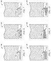
- FIGS. 4-12 illustrate example embodiments of parasitic arms with tunable loads.
- FIGS. 4-12 illustrate a variety of shapes of parasitic arms covered by this disclosure.
- the operating frequency band of a tunable antenna may depend not only on impedance of a tunable load, but also depend on the shape the parasitic arm.
- FIG. 5 is a cut-away view of an embodiment of a parasitic arm 402 and tunable load 404 in a wireless communication device 400.
- FIGS. 6-10 are cut-away views of embodiments of parasitic arms 502, 602, 702, 802, and 902, respectively.
- the parasitic arms in FIGS. 6-10 are coupled to tunable loads 504, 604, 704, 804, and 904, respectively, with the tunable loads connected to a ground plane.
- FIGS. 11 and 12 are cut-away views of embodiments of parasitic arms 1002 and 1102.
- Each of parasitic arms 1002 and 1102 may be coupled to tunable loads 1004 and 1104, respectively, at one end of the parasitic arms.
- each of parasitic arms 1002 and 1102 may be coupled to a ground plane at another end as shown.
- the parasitic arms in FIGS. 5-12 may be electromagnetically coupled to an antenna, such as antenna 204 in FIGS. 3A and 3B .
- FIGS. 5-12 represent portions of wireless communication devices 400-1100, respectively.
- FIG. 13 is a cut-away view of an embodiment of two parasitic arms 1202 and 1206, which may be electromagnetically coupled to an antenna.
- the parasitic arms 1202 and 1206 may be coupled to tunable loads 1204 and 1208, respectively.
- the operating frequency band of a tunable antenna may also depend on the number of parasitic arms and tunable loads.
- FIG. 14 is a side view of another embodiment of a tunable antenna 1300.
- the tunable antenna comprises an antenna 1310 and a parasitic arm 1308.
- the antenna 1310 may reside on a first housing 1304, and the parasitic arm 1308 may reside on a second housing 1308.
- the tunable antenna further comprises a tunable load (not shown).
- FIG. 15 is a side view of another embodiment of a tunable antenna 1400.
- the tunable antenna comprises an antenna 1410 and a parasitic arm 1408.
- the antenna 1410 may reside on a first housing 1406, and the parasitic arm 1408 may reside on a second housing 1404.
- the tunable antenna further comprises a tunable load (not shown).
- FIG. 16A is a cut-away side view of another embodiment of a tunable antenna in a wireless communication device 1500.
- the tunable antenna comprises an antenna 1508 situated on a housing 1504 as shown in FIG. 16A.
- FIG. 16B shows a top view of the tunable antenna.
- the top view illustrates a parasitic arm 1506 as part of the tunable antenna 1500.
- FIG. 16C is also a side view of the tunable antenna but with the connections 1510 and 1512 to ground plane shown (the connections are not shown in FIG. 16A ).
- the connection 1510 connects the parasitic arm 1506 to a ground plane, and the connection 1512 connects the antenna 1508 to the ground plane.
- the tunable antenna may further comprise a tunable load that may be placed between the parasitic arm 1506 and the ground plane.
- FIG. 17A is a cut-away side view of another embodiment of a tunable antenna in a wireless communication device 1600.
- the tunable antenna comprises an antenna 1608 situated on a PCB as shown in FIG. 17A.
- FIG. 17B shows a top view of the tunable antenna.
- the top view illustrates a parasitic arm 1606 as part of the tunable antenna.
- FIG. 17C is also a side view of the tunable antenna but with the connection 1610 to ground plane shown (the connection is not shown in FIG. 17A ).
- the connection 1610 connects the parasitic arm 1606 to a ground plane using a via.
- the tunable antenna may further comprise a tunable load that may be placed between the parasitic arm 1606 and the ground plane.
- the tunable antenna may be on one side of the PCB, and the ground plane may be on an opposing side of the PCB.
- FIGS. 17A-17C demonstrate that a tunable antenna may reside only on a PCB (i.e., may use no housing).
- FIG. 18 is a flowchart 1700 of an embodiment of a method for tuning an antenna.
- an operating frequency band of an antenna is selected or determined.
- the antenna may be employed in a wireless communication device that needs to use a low band in the range of 0.69 GHz to 0.75 GHz.
- a capacitance of a tunable load that corresponds to the selected frequency band of step 1702 is determined.
- the capacitance may be determined by accessing a lookup table, such as Table 1, containing operating frequencies corresponding to capacitance values.
- a capacitance of a tunable load may be adjusted according to the frequency band.
- the steps in the flowchart 1700 may be repeated periodically or at predetermined time intervals or any time a wireless communication device employing the method needs to change operating frequency bands.
- the tunable load may be electromagnetically coupled to the antenna via a parasitic arm, and wherein the operating frequency band depends on the capacitance.
- a processor coupled to the communication device may access a table of related capacitance values and operating frequency bands stored in memory. The table may be generated from laboratory experimentation or simulation models to determine that tuning the capacitance to a certain value results in a specific range of operating frequency bands.
- the processor may look up in the table the capacitance value associated with the requested operating frequency band. The processor may then tune the load on the parasitic arm to the retrieved capacitance value, resulting in the correct tuning of the antenna.
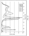
- FIG. 19 is a line graph depicting the return loss for three loads of the tunable antenna illustrated in FIGS. 2A, 2B , 3A, and 3B .
- the tunable load used for these results is a DTC.
- State A represented by a solid line as shown in FIG. 19 , represents return loss when the tunable load has a capacitance of about 5 pF.
- State B represented by a dashed line as shown in FIG. 19 , represents return loss when the tunable load has a capacitance of about 2.5pF.
- FIG. 19 represents a dashed line as shown in FIG. 19 .
- State B the tunable antenna has a return loss of approximately -21 dB at a frequency of 1 GHz, has a return loss of approximately -13 dB at a frequency of 1.75 GHz, and a return loss of 0 dB at a frequency of 2.4 GHz.
- State C represented by a dotted line as shown in FIG. 19 , represents return loss when the tunable load has a capacitance of about 1.8pF. For example, FIG.
- the tunable antenna has a return loss of approximately 0 dB at a frequency of 1.45 GHz, has a return loss of approximately -24 dB at a frequency of 1.5 GHz, and a return loss of -5 dB at a frequency of 2 GHz.
- the results indicate that the tunable antenna in State A may exhibit satisfactory performance for LTE band 17; the tunable antenna in State B may exhibit satisfactory performance at an operating low band frequency of 850 MHz; and the tunable antenna in State C may exhibit satisfactory performance at an operating low band frequency of 900 MHz.
- FIG. 20 shows a line graph depiction the system efficiency for three loads of the tunable antenna illustrated in FIGS. 2A, 2B , 3A, and 3B .
- system efficiency is a measure of how efficiently the power delivered to the antenna can be radiated into free space.
- State A represented by a solid line as shown in FIG. 20 , represents system efficiency when the tunable load has a capacitance of about 5 pF.
- FIG. 20 shows that State A has a system efficiency of 55% at a frequency of approximately 0.7 GHZ, having a peak efficiency of approximately 92% at frequency of 1.78 GHz, and 5% system efficiency at a frequency of 2.5 GHz.
- State B represents return loss when the tunable load has a capacitance of about 2.5 pF.
- FIG. 20 shows that State B has a system efficiency of 45% at a frequency of approximately 1.5 GHZ, having a peak efficiency of approximately 85% at frequency of 0.8 GHz, and 5% system efficiency at a frequency of 2.5 GHz.
- State C represented by a dotted line as shown in FIG. 20 , represents return loss when the tunable load has a capacitance of about 1.8pF.
- FIG. 20 shows that State B has a system efficiency of 45% at a frequency of approximately 1.5 GHZ, having a peak efficiency of approximately 85% at frequency of 0.8 GHz, and 5% system efficiency at a frequency of 2.5 GHz.
- State C represented by a dotted line as shown in FIG. 20 , represents return loss when the tunable load has a capacitance of about 1.8pF.
- the tunable antenna has a system efficiency of 55% at a frequency of approximately 1.0 GHZ, a peak efficiency of approximately 75% at frequency of 0.95 GHz, and a system efficiency of 5% at a frequency of 2.5 GHz.
- FIG. 21 is a schematic diagram of an embodiment of a wireless communication device 2000.
- the communication device 2000 comprises a transceiver 2004, a processor 2006, a memory 2012, and a tunable antenna 2014 as shown in FIG. 21 .
- the tunable antenna 2014 comprises an antenna 2002, a parasitic arm 2008, and a tunable load 2010 as shown in FIG. 21 .
- the tunable antenna 2014 is configured such that the parasitic arm 2008 and the antenna 2002 are electromagnetically coupled.
- the tunable antenna may be configured similarly to the tunable antenna shown in FIGS. 2A, 2B , 3A, and 3B .
- the tunable load 2010 may be any type of tunable load discussed herein, such as a varactor or a MEMS capacitor array.
- the processor 2006 may be implemented as one or more central processing unit or CPU chips, cores (e.g., a multi-core processor), field-programmable gate arrays (FPGAs), application specific integrated circuits (ASICs), and/or digital signal processors (DSPs).
- the tunable load 2010 may be controlled by the processor 2006.
- the processor 2006 may be implemented using hardware, software, or both.
- the memory 2012 may be used to store volatile or non-volatile data including instructions for the processor 2006.
- the memory 2012 may comprise read-only memory (ROM), a random access memory (RAM), and/or secondary storage devices such as tape drives or disk drives.
- the wireless communication device 2000 may be a cellular phone, smart phone, tablet computer, laptop computer or any other type of wireless communication device that needs to employ a plurality of operating bands.
- the wireless communication device 2000 may optionally include a proximity sensor 2016 as shown in FIG. 21 .
- a proximity sensor may detect the proximity of a human head or other objects. An object in close proximity to the wireless communication device 2000 may affect the return loss of the antenna 2002.
- a proximity sensor for example, may comprise a capacitive sensor comprising one or more capacitors to assist in detecting a presence and a proximity of a human body relative to a wireless device.
- the processor 2006 may take into account feedback from the proximity sensor in selecting a capacitance of tunable load 2010.
- the control interface may be Serial Peripheral Interface Bus (SPI), a Mobile Industry Processor Interface (MIPI), or any other suitable interface.
- SPI Serial Peripheral Interface Bus
- MIPI Mobile Industry Processor Interface
- the processor 2006 may be configured to send a control signal to the tunable load 2010 and the tunable load 2006 may be configured to receive the control signal and adjust the capacitance accordingly.
- the memory 2012 may store a table, such as Table 1, of operating frequency bands for the communication device 2000 and associated capacitance values of tunable load 2010 that achieve those frequency bands.
- the processor 2006 may load or access the table from memory 2012. If the communication device 2000 desires to use a frequency band, the processor 2006 may look up the associated capacitance value of the tunable load 2010 in the table and send a control signal to the tunable load to set the capacitance of the tunable load 2010.
- a communication device e.g., a mobile phone
- the processor 2006 may access the table stored in the memory 2012 to see that the associated capacitance value to achieve an operating frequency band of about 870 MHz to 960 MHz is 1.8 pF. The processor 2006 may then adjust the capacitance of the tunable load 2010 to 1.8pF in order to achieve the requested operating frequency band. Further, the table stored in memory may take into account readings from the proximity sensor in the lookup of tunable load. For example, operating frequency band may be a function of a proximity measurement and a tunable load.
- a design that is still subject to frequent change may be preferred to be implemented in software, because re-spinning a hardware implementation is more expensive than re-spinning a software design.
- a design that is stable that will be produced in large volume may be preferred to be implemented in hardware, for example in an ASIC, because for large production runs the hardware implementation may be less expensive than the software implementation.
- a design may be developed and tested in a software form and later transformed, by well-known design rules, to an equivalent hardware implementation in an application specific integrated circuit that hardwires the instructions of the software. In the same manner as a machine controlled by a new ASIC is a particular machine or apparatus, likewise a computer that has been programmed and/or loaded with executable instructions may be viewed as a particular machine or apparatus.
- R R1 + k ⁇ (Ru - R1), wherein k is a variable ranging from 1 percent to 100 percent with a 1 percent increment, i.e., k is 1 percent, 2 percent, 3 percent, 4 percent, 5 percent, ..., 50 percent, 51 percent, 52 percent, ..., 95 percent, 96 percent, 97 percent, 98 percent, 99 percent, or 100 percent.
- k is a variable ranging from 1 percent to 100 percent with a 1 percent increment, i.e., k is 1 percent, 2 percent, 3 percent, 4 percent, 5 percent, ..., 50 percent, 51 percent, 52 percent, ..., 95 percent, 96 percent, 97 percent, 98 percent, 99 percent, or 100 percent.
- any numerical range defined by two R numbers as defined in the above is also specifically disclosed.
- references to "one embodiment,” “an embodiment,” “some embodiment,” “various embodiments,” or the like, indicate that a particular element or characteristic is included in at least one embodiment of the invention. Although the phrases may appear in various places, the phrases do not necessarily refer to the same embodiment.
Landscapes
- Engineering & Computer Science (AREA)
- Computer Networks & Wireless Communication (AREA)
- Signal Processing (AREA)
- Support Of Aerials (AREA)
- Details Of Aerials (AREA)
- Transceivers (AREA)
- Near-Field Transmission Systems (AREA)
- Input Circuits Of Receivers And Coupling Of Receivers And Audio Equipment (AREA)
Description
- Wireless communication technologies and services continue to proliferate leading to new voice and data services, carrier aggregation, and new demands on roaming to name a few. As technologies advance and user demand for services increases, wireless communication devices need to support an increasing number of operating frequency bands to support the technologies and services. At the same time, wireless communication devices are getting smaller. For example, mobile phones are becoming increasingly thinner, and as a result there may be less volume available for antenna structures and systems, as well as less space for the coexistence of electromechanical components around the antenna.
- For example,
WO 2011/059088A1 refers to an antenna device comprising an antenna element disposed on a mounting board separate from a main circuit board, a coupling means disposed on the mounting board such that it is electromagnetically coupled to the antenna element, and a frequency-adjusting means disposed on the mounting board such that it is connected to the coupling means, the antenna element comprising first and second strip-shaped antenna elements integrally connected for sharing a feeding point, the second antenna element being shorter than the first antenna element; the coupling means being formed on a dielectric chip attached to the mounting board, and having a coupling electrode electromagnetically coupled to part of the first antenna element. The frequency-adjusting means comprises a parallel resonance circuit comprising a variable capacitance circuit and a first inductance element, and a second inductance element series-connected to the parallel resonance circuit. - Further,
US 2003/0210203A1 refers to an adaptive antenna system having a counterpoise conductor contained within a housing of a communication device and located distally from such surfaces of the housing that can be held by or placed in proximity to a user or external objects which detune the counterpoise. A tuning circuit is coupled between the counterpoise conductor and a ground. The tuning circuit is operable to adapt the resonant frequency of the counterpoise conductor to divert operational RF currents away from the ground located in proximity the user or external objects and onto the counterpoise conductor. - Further,
US 2006/0252391A1 refers to an apparatus, system and method optimizing antenna performance using tunable parasitic elements by changing antenna characteristics based on signal quality parameters of electromagnetic signals exchanged through the antenna. The tunable parasitic elements are responsive to control signals to modify current flowing through a counterpoise of the antenna. Based on signal quality parameters received from a communication system, transmission characteristics are optimized by increasing the transmission gain in the direction of the receiving base station. Signal quality parameters measured at the antenna are used to change reception characteristics by minimizing reception gain in the direction of a jamming transmitter. - Further,
US 2009/0224991A1 refers to an antenna comprising an IMD element, and one or more parasitic and active tuning elements. The IMD element, when used in combination with the active tuning and parasitic elements, allows antenna operation at multiple resonant frequencies. In addition, the direction of antenna radiation pattern may be arbitrarily rotated in accordance with the parasitic and active tuning elements. - Smaller devices may result in the need for more compact antennas. However, more compact antennas may not cover enough frequency bands for satisfactory operation. These opposing trends - increasing demands on antennas while shrinking the volume available for antennas - lead to a need for improved antenna designs. Thus, there is a need to provide an antenna compact enough to fit in modern wireless communication devices while covering frequency bands demanded for various services.
- In a first aspect an apparatus is provided comprising:
- an antenna, wherein the antenna is a dual-arm antenna having two arms, the two arms have different lengths with ends facing each other without overlapping each other;
- a parasitic arm electromagnetically coupled to the antenna, wherein the parasitic arm is disposed between the two ends of the two arms; and
- a tunable load coupled to the parasitic arm, wherein a capacitance of the tunable load is variable, and wherein an operating frequency band of the antenna depends on the capacitance,
- wherein the antenna resides on a housing of the apparatus, and the parasitic arm resides on a printed circuit board, PCB, of the apparatus, wherein the housing allows the antenna to be physically separated from the PCB and the housing is connected to the PCB.
- In a first implementation form of the first aspect the capacitance of the tunable load is tunable in the range of about 1.8 picofarads (pF) to about 5 picofarads, wherein if the tunable load is about 1.8 pF an operating frequency low band is about 0.69 gigahertz (GHz) to about 0.75 GHz and an operating frequency high band of is about 1.66 GHz to about 2.26 GHz, wherein if the tunable load is about 2.5 pF the operating frequency low band is about 0.81 GHz to about 0.89 GHz and the operating frequency high band is about 1.74 GHz to 2.27 GHz, and wherein if the tunable load is about 1.8 pF the operating frequency low band is about 0.87 GHz to about 0.96 GHz and the operating frequency high band is about 1.42 GHz to about 1.59 GHz.
- In a second implementation form of the first aspect the apparatus is a wireless communication device, wherein the apparatus further comprises:
a processor coupled to the tunable load and configured to: - select a first operating frequency band; and
- set the capacitance to a value to achieve the first operating frequency band.
- In a third implementation form of the first aspect the apparatus further comprises:
- a memory coupled to the processor;
- wherein the processor is further configured to:
- access a table stored in the memory, the table containing at least one capacitance value related to at least one operating frequency band; and
- retrieve a capacitance value related to the first operating frequency band in the table,
- wherein the setting the capacitance to the value to achieve the first operating frequency band further comprises sending a control signal to the tunable load to set the capacitance to the capacitance value related to the first operating frequency band in the table.
- In a fourth implementation form of the first aspect the apparatus further comprises a proximity sensor coupled to the processor, wherein the processor is further configured to receive a proximity sensor measurement and take the proximity sensor measurement into account in selecting the first operating frequency band.
- These and other features will be more clearly understood from the following detailed description taken in conjunction with the accompanying drawings and claims. The embodiments that do not fall within the scope of the claims shall be treated as examples.
- For a more complete understanding of this disclosure, reference is now made to the following brief description, taken in connection with the accompanying drawings and detailed description, wherein like reference numerals represent like parts.
-
FIG. 1 is a schematic diagram of an embodiment of a tunable antenna. -
FIGS. 2A and 2B are cut-away views of an embodiment of a tunable antenna. -
FIGS. 3A and 3B are perspective cut-away views of an embodiment of a tunable antenna. -
FIG. 4 is a block diagram of a general tunable load that may be used in a wireless device. -
FIGS. 5-13 are cut-away views of different embodiments of parasitic arms with tunable loads. -
FIG. 14 is a side view of another embodiment of a tunable antenna. -
FIG. 15 is a side view of yet another embodiment of a tunable antenna. -
FIGS. 16A, 16B , and16C are various cut-away views of yet another embodiment of a tunable antenna. -
FIGS. 17A, 17B, and 17C are various cut-away views of yet another embodiment of a tunable antenna. -
FIG. 18 is a flowchart of an embodiment of a tunable antenna method. -
FIG. 19 is a line graph showing the return loss for three loads of a tunable antenna. -
FIG. 20 is a line graph showing the system efficiency of three loads of a tunable antenna. -
FIG. 21 is a schematic diagram of an embodiment of a communication device - It should be understood at the outset that, although an illustrative implementation of one or more embodiments are provided below, the disclosed systems and/or methods may be implemented using any number of techniques, whether currently known or in existence. The disclosure should in no way be limited to the illustrative implementations, drawings, and techniques illustrated below, including the exemplary designs and implementations illustrated and described herein, but may be modified within the scope of the appended claims along with their full scope of equivalents. While certain aspects of conventional technologies have been discussed to facilitate the present disclosure, applicants in no way disclaim these technical aspects, and it is contemplated that the present disclosure may encompass one or more of the conventional technical aspects discussed herein.
- Disclosed herein is a tunable antenna. For example, operating frequency bands of the tunable antenna may be adjusted by varying a load of a parasitic arm electromagnetically coupled to an antenna. Also disclosed herein is a method of tuning an antenna. For example, the antenna may be tuned by adjusting a load of a parasitic arm electromagnetically coupled to the antenna. The tunable antenna apparatuses and methods may be suitable for implementation in compact wireless communication devices.
-
Figure 1 is a schematic diagram of an embodiment of a tunable antenna. Thetunable antenna 100 comprises anantenna 102, afeed line 110, aparasitic arm 104, and atunable load 106 configured as shown inFIG. 1 . Theantenna 102 may be coupled to a transceiver (not shown) via theantenna feed line 110. Theparasitic arm 104 is located in close enough proximity with theantenna 102 to be coupled to theantenna 102 electromagnetically. However, as shown there may be no direct connection between theparasitic arm 104 and theantenna 102. Further, theparasitic arm 104 may be coupled to atunable load 106. Thetunable load 106 may be connected to ground as shown or may be maintained at a substantially constant non-zero voltage level. The tunable load may have a variable or tunable impedance (i.e., combination of resistance, capacitance, and/or inductance). For example, a fixed or non-tunable inductor may be placed in series with a tunable capacitor to provide a variable impedance. The tunable capacitor may be implemented as a radio frequency (RF) switching device, a varactor, a single pole multi throw ("SPxT") switch, a digital tunable capacitor ("DTC"), or a micro-electromechanical system ("MEMS") capacitor array. These are illustrative examples as thetunable load 106 may be implemented by any suitable technology. - The
antenna 102 may be any antenna type that allows for variable and continuous tuning by adjusting thetunable load 106. Such antenna types include but are not limited to inverted-F antennas ("IFAs"), loop antennas, slot antennas, or folded inverted conformal antennas (FICAs). - Regardless of the type of antenna or tunable load used, the
parasitic arm 104 and theantenna 102 are coupled to each other electromagnetically. Theparasitic arm 104 may be tuned separately from the antenna by varying thetunable load 106 coupled to the parasitic arm. Varying the tunable load affects the operating frequency band of theantenna 102, thus adjusting at least one operating parameter of theantenna 102 without the need to add capacitance directly to the antenna. - Continuous tuning of the
antenna 102 may be possible if tuning capabilities of thetunable load 106 are continuous. For example, because both a DTC and a MEMS capacitor array may be continuously tunable, the selection of either of these tunable loads may result in a continuously tunable antenna. Further, the antenna apparatus may be implemented to enable dynamically tunable configurations with suitable feedback mechanism for mitigating different antenna loadings, such as the front proximity sensor for head detection, or other sensors/detectors. For example, the capacitance of thetunable load 106 may be in the range of 1.8 picofarads (pF) to 5 pF with different loads resulting in different bands for theantenna 102 as shown in Table 1. The inductance of the tunable load may be relatively constant at about 10 nanohenries (nH). (In Table 1 the "Low Band" may have a return loss less than - 4 decibels (dB), and the "High Band" may have a return loss of less than -6 dB). As shown in Table 1, with a loading of the parasitic arm of about 1.8 pF, the low band may be in the range of about 870 megahertz (MHz) to 960 MHz and the high band may be in the range of about 1.42 to 1.59 gigahertz (GHz); with a loading of the parasitic arm of about 2.5 pF, the low band may be in the range of about 810 MHz to 890 MHz and the high band may be in the range of about 1.74 GHz to 2.27 GHz; and with loading of the parasitic arm of about 5 pF, the low band may be in the range of about 690 MHz to 750 MHz, and the high band may be in the range of 1.66 GHz to 2.26 GHz. By adjusting thetunable load 106, the antenna performance may be tuned for a predefined frequency band, or a particular operating channel, depending on the requirements of a wireless device employing thetunable antenna 100. A tunable antenna with the characteristics of Table 1 may support Long Term Evolution (LTE)bands 11, 12, 13, 17, 18, 19, and 21, as examples, asbands 12, 13, 17, 18, and 19 may be in a range from 690 MHz to 960 MHz and bands 11 and 21 may be in a range from 1.42 GHz to 1.51 GHz. Such a tunable antenna may also support multiple Universal Mobile Telecommunications System ("UMTS")/Wideband Code Division Multiple Access (W-CDMA)/Global System for Mobile Communications ("GSM") frequency bands, such as frequency bands located at 850 MHz, 900 MHz, 1800 MHz, and 1900 MHz.Table 1. Low Band and High Band for various loads in a tunable antenna embodiment. Loading of parasitic arm Low band High band 1.8 pF 870 MHz-960 MHz 1.42 GHz-1.59 GHz 2.5 pF 810 MHz-890 MHz 1.74 GHz-2.27 GHz 5 pF 690 MHz-750 MHz 1.66 GHz-2.26 GHz - Since adjusting the operating frequency band of the antenna is enabled by varying the tuning load on the parasitic arm, the antenna performance enables a wider range of bandwidths without the need for a larger antenna. Thus, as a result of being able to keep the antenna smaller while increasing the performance, the volume of area needed for the antenna apparatus as a whole may be decreased, enabling production of smaller devices.
- In designing the antenna apparatus, the amount of electrical energy from surrounding circuitry components, as well as outside environmental influences, may be taken into consideration. For example, antenna performance may be affected by additional electrical energy within the surrounding circuit board as emitted by neighboring circuitry components. For this reason, the antenna(s) may be placed in a region, sometimes referred to as a "keepout" area, that does not include copper (e.g., grounding) or electrical components on the PCB. A keepout area may be intended to keep the antenna(s) away from any nearby conductors or electrical components that could degrade antenna performance. Additionally, the antenna apparatus may be affected by outside environmental issues (e.g., the proximity of a user's head to a mobile device containing the antenna apparatus).
-
FIGS. 2A and 2B are cut-away views of an embodiment of a tunable antenna in awireless communication device 200. The tunable antenna comprises anantenna 204 and aparasitic arm 206. BothFIG. 2A and FIG. 2B show an x-y plane view of an examplewireless communication device 200 comprising aparasitic arm 206; however,FIG. 2B omits the antenna for a clearer view of the parasitic element coupling. In particular,FIG. 2A shows an example placement, shape, and size ofparasitic arm 206 in relation to the apparatus as a whole. - Referring again to
FIG. 2A , theparasitic arm 206, which may be made of a conductive material (e.g. copper), is traced onto a printed circuit board (PCB) and is electromagnetically coupled toantenna 204. In many cases, the PCB may be FR4, which may be a glass-reinforced epoxy laminate. Both theparasitic arm 206 and theantenna 204 are supported and encapsulated within thekeepout area 202 of the PCB. Because theparasitic arm 206 is electromagnetically coupled to theantenna 204, and does not require physical coupling to theantenna 204, theparasitic arm 206 may be placed at a plurality of locations in proximity to theantenna 204. For example, there may be a four millimeter space between the parasitic arm and the antenna. - In order to more clearly understand the placement and coupling of the parasitic arm,
FIG. 2B shows the antenna apparatus with the antenna removed. In particular,parasitic arm 206 is located within the nonconductive keepoutarea 202 and coupled to atunable load 208. Both theparasitic arm 206 and thetunable load 208 are electromagnetically coupled but not physically coupled to the antenna. Theparasitic arm 206 has a fixed inductance, and thetunable load 208 comprises a tunable capacitor. Thetunable load 208 may further comprise a fixed inductor in parallel with the tunable capacitor. The combination of theparasitic arm 206 and thetunable load 208 may be viewed as a variable impedance. Thetunable load 208 may be connected to aground plane 216. As understood by one of skill in the art, aground plane 216 may be a substantially flat conducting surface. Further, although not shown in the figure there may be other electrical components occupying some of the area shown as being occupied by theground plane 216. -
FIG. 3A shows a perspective cut-away view of thewireless communication device 200 in order to further illustrate the relationship of theparasitic arm 206 with respect to theantenna 204. As shown inFIG. 3A , theparasitic arm 206 may be located above theantenna element 204, and between to the two ends of theantenna element 204. Further,FIG. 3A illustrates anantenna feed line 210, as well as theantenna ground line 212, to which theantenna 204 is coupled. Thefeed line 210 couples theantenna 204 to a transceiver and theantenna ground line 212 couples theantenna 204 to ground. -
Antenna 204 may reside on an antenna carrier, or plastic housing (not shown), which resides four millimeters above the PCB. Theparasitic arm 206 may be printed on the PCB and thus may reside four millimeters below theantenna 204. -
FIG. 3B shows the same perspective cut-away view of thewireless communication device 200 ofFIG. 3A , but with thehousing 214 shown. Note that a view of theparasitic arm 206, theantenna feed line 210, andantenna ground line 212 is obstructed by thehousing 214. Thehousing 214 provides a surface separated from the PCB on which all or part of theantenna 204 may reside. For example, theantenna 204 may be deposited or traced onto thehousing 214. - The tunable antenna configuration illustrated in
FIGS. 2A, 2B ,3A, and 3B may be used to achieve the results presented in Table 1. The relationship shown inFIGS. 2A, 2B ,3A, and 3B is one example of many possible relationships between an antenna, such asantenna 204, and a parasitic arm, such asparasitic arm 206, that result in electromagnetic coupling. The tunable load used for the results in Table 1 (and the results ofFIGS. 18 and19 below) is a DTC in parallel with a fixed inductor. -
FIG. 4 is a block diagram of a generaltunable load 300 that may be used in a wireless device. Thetunable load 300 comprisesparasitic arm 310 and avariable impedance 320. The tunable load may optionally include a fixedimpedance 330 and a fixedimpedance 340 connected to ground (or a ground plane) as shown. Each of the fixedimpedances variable impedance 320 may be a tunable capacitor. Thus, the fixedimpedance 330 may be in parallel with thevariable impedance 320, and the combination may be in series with a fixedimpedance 340. Thetunable load 300 may be electromagnetically coupled to an antenna via theparasitic arm 310. - The size of the parasitic arm may vary depending on the needs of the device utilizing the antenna apparatus. For example, in one embodiment, the parasitic arm may be of a larger size to enable a wider range of accessible bandwidths. In another embodiment, however, the parasitic arm may be of a smaller size on order to provide tuning of the antenna in a smaller device, such as a small and/or thin handheld mobile device.
- The parasitic arm is not restrained to only one shape as the shape of the parasitic arm may vary depending on the needs of the device utilizing the antenna apparatus. For example, in one embodiment, the device may be a rectangular shaped smart phone comprising a rectangular shaped printed circuit board (PCB). Thus, in one embodiment, the shape of the parasitic arm may be "L" shaped in order to enable optimal coupling for a rectangular PCB. However, in another embodiment, in order to enable performance of the antenna tuning, the parasitic arm may be of another shape, such as a straight line or an "S" shape.
- In one example embodiment, the device containing the antenna apparatus may be a handheld wireless device such as a mobile phone. In this embodiment, the mobile phone may be four inches across, with a keepout area measuring 9 millimeters (mm) thick. The load of the
parasitic arm 206 may have a capacitor tuning range of about 1.8 pF to 5 pF, yielding a ratio between smallest and largest capacitance of approximately 1 to 2.7. - A tunable antenna according to this disclosure is not limited to the particular embodiments in
FIGS. 2A, 2B ,3A, and 3B , as those figures illustrate an example exemplary embodiment. Tunable antennas according to this disclosure may have a variety of embodiments.FIGS. 4-12 illustrate example embodiments of parasitic arms with tunable loads.FIGS. 4-12 illustrate a variety of shapes of parasitic arms covered by this disclosure. The operating frequency band of a tunable antenna may depend not only on impedance of a tunable load, but also depend on the shape the parasitic arm. -
FIG. 5 is a cut-away view of an embodiment of aparasitic arm 402 andtunable load 404 in awireless communication device 400. Likewise,FIGS. 6-10 are cut-away views of embodiments ofparasitic arms FIGS. 6-10 are coupled totunable loads FIGS. 11 and 12 are cut-away views of embodiments ofparasitic arms parasitic arms tunable loads parasitic arms FIGS. 5-12 may be electromagnetically coupled to an antenna, such asantenna 204 inFIGS. 3A and 3B .FIGS. 5-12 represent portions of wireless communication devices 400-1100, respectively. -
FIG. 13 is a cut-away view of an embodiment of twoparasitic arms parasitic arms tunable loads 1204 and 1208, respectively. Thus, the operating frequency band of a tunable antenna may also depend on the number of parasitic arms and tunable loads. -
FIG. 14 is a side view of another embodiment of atunable antenna 1300. The tunable antenna comprises anantenna 1310 and aparasitic arm 1308. Theantenna 1310 may reside on afirst housing 1304, and theparasitic arm 1308 may reside on asecond housing 1308. The tunable antenna further comprises a tunable load (not shown). -
FIG. 15 is a side view of another embodiment of atunable antenna 1400. The tunable antenna comprises anantenna 1410 and aparasitic arm 1408. Theantenna 1410 may reside on afirst housing 1406, and theparasitic arm 1408 may reside on asecond housing 1404. The tunable antenna further comprises a tunable load (not shown). -
FIG. 16A is a cut-away side view of another embodiment of a tunable antenna in awireless communication device 1500. The tunable antenna comprises anantenna 1508 situated on ahousing 1504 as shown inFIG. 16A. FIG. 16B shows a top view of the tunable antenna. The top view illustrates aparasitic arm 1506 as part of thetunable antenna 1500.FIG. 16C is also a side view of the tunable antenna but with theconnections FIG. 16A ). Theconnection 1510 connects theparasitic arm 1506 to a ground plane, and theconnection 1512 connects theantenna 1508 to the ground plane. The tunable antenna may further comprise a tunable load that may be placed between theparasitic arm 1506 and the ground plane. -
FIG. 17A is a cut-away side view of another embodiment of a tunable antenna in awireless communication device 1600. The tunable antenna comprises anantenna 1608 situated on a PCB as shown inFIG. 17A. FIG. 17B shows a top view of the tunable antenna. The top view illustrates aparasitic arm 1606 as part of the tunable antenna.FIG. 17C is also a side view of the tunable antenna but with theconnection 1610 to ground plane shown (the connection is not shown inFIG. 17A ). Theconnection 1610 connects theparasitic arm 1606 to a ground plane using a via. The tunable antenna may further comprise a tunable load that may be placed between theparasitic arm 1606 and the ground plane. The tunable antenna may be on one side of the PCB, and the ground plane may be on an opposing side of the PCB.FIGS. 17A-17C demonstrate that a tunable antenna may reside only on a PCB (i.e., may use no housing). -
FIG. 18 is aflowchart 1700 of an embodiment of a method for tuning an antenna. Instep 1702 an operating frequency band of an antenna is selected or determined. For example, the antenna may be employed in a wireless communication device that needs to use a low band in the range of 0.69 GHz to 0.75 GHz. Instep 1703, a capacitance of a tunable load that corresponds to the selected frequency band ofstep 1702 is determined. The capacitance may be determined by accessing a lookup table, such as Table 1, containing operating frequencies corresponding to capacitance values. In step 1704 a capacitance of a tunable load may be adjusted according to the frequency band. The steps in theflowchart 1700 may be repeated periodically or at predetermined time intervals or any time a wireless communication device employing the method needs to change operating frequency bands. - In the method for tuning an antenna described in
FIG. 18 , the tunable load may be electromagnetically coupled to the antenna via a parasitic arm, and wherein the operating frequency band depends on the capacitance. In one embodiment, a processor coupled to the communication device may access a table of related capacitance values and operating frequency bands stored in memory. The table may be generated from laboratory experimentation or simulation models to determine that tuning the capacitance to a certain value results in a specific range of operating frequency bands. When a communication device requests a specific operating frequency band, the processor may look up in the table the capacitance value associated with the requested operating frequency band. The processor may then tune the load on the parasitic arm to the retrieved capacitance value, resulting in the correct tuning of the antenna. -
FIG. 19 is a line graph depicting the return loss for three loads of the tunable antenna illustrated inFIGS. 2A, 2B ,3A, and 3B . The tunable load used for these results is a DTC. State A, represented by a solid line as shown inFIG. 19 , represents return loss when the tunable load has a capacitance of about 5 pF. State B, represented by a dashed line as shown inFIG. 19 , represents return loss when the tunable load has a capacitance of about 2.5pF. In particular,FIG. 19 shows that for State B the tunable antenna has a return loss of approximately -21 dB at a frequency of 1 GHz, has a return loss of approximately -13 dB at a frequency of 1.75 GHz, and a return loss of 0 dB at a frequency of 2.4 GHz. State C, represented by a dotted line as shown inFIG. 19 , represents return loss when the tunable load has a capacitance of about 1.8pF. For example,FIG. 19 shows that for State C the tunable antenna has a return loss of approximately 0 dB at a frequency of 1.45 GHz, has a return loss of approximately -24 dB at a frequency of 1.5 GHz, and a return loss of -5 dB at a frequency of 2 GHz. As shown inFIG. 19 , the results indicate that the tunable antenna in State A may exhibit satisfactory performance forLTE band 17; the tunable antenna in State B may exhibit satisfactory performance at an operating low band frequency of 850 MHz; and the tunable antenna in State C may exhibit satisfactory performance at an operating low band frequency of 900 MHz. -
FIG. 20 shows a line graph depiction the system efficiency for three loads of the tunable antenna illustrated inFIGS. 2A, 2B ,3A, and 3B . As understood by one of skill in the art, system efficiency is a measure of how efficiently the power delivered to the antenna can be radiated into free space. State A, represented by a solid line as shown inFIG. 20 , represents system efficiency when the tunable load has a capacitance of about 5 pF. In particular,FIG. 20 shows that State A has a system efficiency of 55% at a frequency of approximately 0.7 GHZ, having a peak efficiency of approximately 92% at frequency of 1.78 GHz, and 5% system efficiency at a frequency of 2.5 GHz. State B, represented by a dashed line as shown inFIG. 20 , represents return loss when the tunable load has a capacitance of about 2.5 pF. In particular,FIG. 20 shows that State B has a system efficiency of 45% at a frequency of approximately 1.5 GHZ, having a peak efficiency of approximately 85% at frequency of 0.8 GHz, and 5% system efficiency at a frequency of 2.5 GHz. State C, represented by a dotted line as shown inFIG. 20 , represents return loss when the tunable load has a capacitance of about 1.8pF. For example,FIG. 20 shows that in State C the tunable antenna has a system efficiency of 55% at a frequency of approximately 1.0 GHZ, a peak efficiency of approximately 75% at frequency of 0.95 GHz, and a system efficiency of 5% at a frequency of 2.5 GHz. -
FIG. 21 is a schematic diagram of an embodiment of awireless communication device 2000. Thecommunication device 2000 comprises atransceiver 2004, aprocessor 2006, amemory 2012, and atunable antenna 2014 as shown inFIG. 21 . Thetunable antenna 2014 comprises anantenna 2002, aparasitic arm 2008, and atunable load 2010 as shown inFIG. 21 . Thetunable antenna 2014 is configured such that theparasitic arm 2008 and theantenna 2002 are electromagnetically coupled. For example, the tunable antenna may be configured similarly to the tunable antenna shown inFIGS. 2A, 2B ,3A, and 3B . Thetunable load 2010 may be any type of tunable load discussed herein, such as a varactor or a MEMS capacitor array. Theprocessor 2006 may be implemented as one or more central processing unit or CPU chips, cores (e.g., a multi-core processor), field-programmable gate arrays (FPGAs), application specific integrated circuits (ASICs), and/or digital signal processors (DSPs). Thetunable load 2010 may be controlled by theprocessor 2006. Theprocessor 2006 may be implemented using hardware, software, or both. Thememory 2012 may be used to store volatile or non-volatile data including instructions for theprocessor 2006. Thememory 2012 may comprise read-only memory (ROM), a random access memory (RAM), and/or secondary storage devices such as tape drives or disk drives. Thewireless communication device 2000 may be a cellular phone, smart phone, tablet computer, laptop computer or any other type of wireless communication device that needs to employ a plurality of operating bands. - The
wireless communication device 2000 may optionally include aproximity sensor 2016 as shown inFIG. 21 . A proximity sensor may detect the proximity of a human head or other objects. An object in close proximity to thewireless communication device 2000 may affect the return loss of theantenna 2002. A proximity sensor, for example, may comprise a capacitive sensor comprising one or more capacitors to assist in detecting a presence and a proximity of a human body relative to a wireless device. A person of skill in the art will recognize that there are many types of available proximity sensors. Therefore, theprocessor 2006 may take into account feedback from the proximity sensor in selecting a capacitance oftunable load 2010. - There may be a control interface between the
processor 2006 and thetunable load 2010 to allow theprocessor 2006 to control thetunable load 2010. The control interface may be Serial Peripheral Interface Bus (SPI), a Mobile Industry Processor Interface (MIPI), or any other suitable interface. Theprocessor 2006 may be configured to send a control signal to thetunable load 2010 and thetunable load 2006 may be configured to receive the control signal and adjust the capacitance accordingly. - The
memory 2012 may store a table, such as Table 1, of operating frequency bands for thecommunication device 2000 and associated capacitance values oftunable load 2010 that achieve those frequency bands. Theprocessor 2006 may load or access the table frommemory 2012. If thecommunication device 2000 desires to use a frequency band, theprocessor 2006 may look up the associated capacitance value of thetunable load 2010 in the table and send a control signal to the tunable load to set the capacitance of thetunable load 2010. For example, a communication device (e.g., a mobile phone) may request an operating frequency band of about 870 MHz to 960 MHz. Using Table 1 as an example, theprocessor 2006 may access the table stored in thememory 2012 to see that the associated capacitance value to achieve an operating frequency band of about 870 MHz to 960 MHz is 1.8 pF. Theprocessor 2006 may then adjust the capacitance of thetunable load 2010 to 1.8pF in order to achieve the requested operating frequency band. Further, the table stored in memory may take into account readings from the proximity sensor in the lookup of tunable load. For example, operating frequency band may be a function of a proximity measurement and a tunable load. - It is understood that by programming and/or loading executable instructions onto the
communication device 2000, at least one of theprocessor 2006 or thememory 2012 may be changed, transforming thecommunication device 2000 in part into a particular machine or apparatus having the novel functionality taught by the present disclosure, such as themethod 1700. It is fundamental to the electrical engineering and software engineering arts that functionality that can be implemented by loading executable software into a computer can be converted to a hardware implementation by well-known design rules. Decisions between implementing a concept in software versus hardware typically hinge on considerations of stability of the design and numbers of units to be produced rather than any issues involved in translating from the software domain to the hardware domain. Generally, a design that is still subject to frequent change may be preferred to be implemented in software, because re-spinning a hardware implementation is more expensive than re-spinning a software design. Generally, a design that is stable that will be produced in large volume may be preferred to be implemented in hardware, for example in an ASIC, because for large production runs the hardware implementation may be less expensive than the software implementation. Often a design may be developed and tested in a software form and later transformed, by well-known design rules, to an equivalent hardware implementation in an application specific integrated circuit that hardwires the instructions of the software. In the same manner as a machine controlled by a new ASIC is a particular machine or apparatus, likewise a computer that has been programmed and/or loaded with executable instructions may be viewed as a particular machine or apparatus. - At least one embodiment is disclosed and variations, combinations, and/or modifications of the embodiment(s) and/or features of the embodiment(s) made by a person having ordinary skill in the art are within the scope of the disclosure. Alternative embodiments that result from combining, integrating, and/or omitting features of the embodiment(s) are also within the scope of the disclosure. Where numerical ranges or limitations are expressly stated, such express ranges or limitations should be understood to include iterative ranges or limitations of like magnitude falling within the expressly stated ranges or limitations (e.g., from about 1 to about 10 includes, 2, 3, 4, etc.; greater than 0.10 includes 0.11, 0.12, 0.13, etc.). For example, whenever a numerical range with a lower limit, Rl, and an upper limit, Ru, is disclosed, any number falling within the range is specifically disclosed. In particular, the following numbers within the range are specifically disclosed: R = R1 + k ∗ (Ru - R1), wherein k is a variable ranging from 1 percent to 100 percent with a 1 percent increment, i.e., k is 1 percent, 2 percent, 3 percent, 4 percent, 5 percent, ..., 50 percent, 51 percent, 52 percent, ..., 95 percent, 96 percent, 97 percent, 98 percent, 99 percent, or 100 percent. Moreover, any numerical range defined by two R numbers as defined in the above is also specifically disclosed. Use of the term "optionally" with respect to any element of a claim means that the element is required, or alternatively, the element is not required, both alternatives being within the scope of the claim. Use of broader terms such as comprises, includes, and having should be understood to provide support for narrower terms such as consisting of, consisting essentially of, and comprised substantially of. Accordingly, the scope of protection is not limited by the description set out above but is defined by the claims that follow.
- References to "one embodiment," "an embodiment," "some embodiment," "various embodiments," or the like, indicate that a particular element or characteristic is included in at least one embodiment of the invention. Although the phrases may appear in various places, the phrases do not necessarily refer to the same embodiment.
- The above discussion is meant to be illustrative of the principles and various embodiments of the present invention. Numerous variations and modifications will become apparent to those skilled in the art once the above disclosure is fully appreciated. For example, while the various embodiments have been described in terms of a variable tunable antenna coupled to a parasitic arm, this context shall not be read as a limitation as to the scope of one or more of the embodiments described - the same techniques may be used for other embodiments. It is intended that the following claims be interpreted to embrace all such various and modifications.
Claims (5)
- An apparatus (2000) comprising:an antenna (2002), wherein the antenna (2002) is a dual-arm antenna having two arms, the two arms have different lengths with ends facing each other without overlapping each other;a parasitic arm (2008) electromagnetically coupled to the antenna (2002), wherein the parasitic arm (2008) is disposed between the two ends of the two arms; anda tunable load (2010) coupled to the parasitic arm (2008), wherein a capacitance of the tunable load (2010) is variable, and wherein an operating frequency band of the antenna (2002) depends on the capacitance,wherein the antenna (2002) resides on a housing (214) of the apparatus (2000), and the parasitic arm (2008) resides on a printed circuit board, PCB, of the apparatus (2000),wherein the housing (214) allows the antenna (2002) to be physically separated from the PCB and the housing is (214) connected to the PCB.
- The apparatus (2000) of claim 1, wherein the capacitance of the tunable load (2010) is tunable in the range of about 1.8 picofarads (pF) to about 5 picofarads, wherein if the tunable load is about 1.8 pF an operating frequency low band is about 0.69 gigahertz (GHz) to about 0.75 GHz and an operating frequency high band of is about 1.66 GHz to about 2.26 GHz, wherein if the tunable load is about 2.5 pF the operating frequency low band is about 0.81 GHz to about 0.89 GHz and the operating frequency high band is about 1.74 GHz to 2.27 GHz, and wherein if the tunable load is about 1.8 pF the operating frequency low band is about 0.87 GHz to about 0.96 GHz and the operating frequency high band is about 1.42 GHz to about 1.59 GHz.
- The apparatus (2000) of claim 1,
wherein the apparatus (2000) is a wireless communication device, wherein the apparatus (2000) further comprises:
a processor (2006) coupled to the tunable load (2010) and configured to:select a first operating frequency band; andset the capacitance to a value to achieve the first operating frequency band. - The apparatus of claim 3, further comprising:
a memory (2012) coupled to the processor (2006);
wherein the processor (2006) is further configured to:access a table stored in the memory, the table containing at least one capacitance value related to at least one operating frequency band; andretrieve a capacitance value related to the first operating frequency band in the table,wherein the setting the capacitance to the value to achieve the first operating frequency band further comprises sending a control signal to the tunable load to set the capacitance to the capacitance value related to the first operating frequency band in the table. - The apparatus of claim 4, further comprising a proximity sensor (2016) coupled to the processor (2006), wherein the processor (2006) is further configured to receive a proximity sensor measurement and take the proximity sensor measurement into account in selecting the first operating frequency band.
Applications Claiming Priority (2)
| Application Number | Priority Date | Filing Date | Title |
|---|---|---|---|
| US13/732,097 US10122402B2 (en) | 2012-12-31 | 2012-12-31 | Method and apparatus for a tunable antenna |
| PCT/CN2013/089814 WO2014101695A1 (en) | 2012-12-31 | 2013-12-18 | Method and apparatus for a tunable antenna |
Publications (3)
| Publication Number | Publication Date |
|---|---|
| EP2920844A1 EP2920844A1 (en) | 2015-09-23 |
| EP2920844A4 EP2920844A4 (en) | 2015-12-02 |
| EP2920844B1 true EP2920844B1 (en) | 2020-02-12 |
Family
ID=51017717
Family Applications (1)
| Application Number | Title | Priority Date | Filing Date |
|---|---|---|---|
| EP13868648.0A Active EP2920844B1 (en) | 2012-12-31 | 2013-12-18 | Method and apparatus for a tunable antenna |
Country Status (6)
| Country | Link |
|---|---|
| US (1) | US10122402B2 (en) |
| EP (1) | EP2920844B1 (en) |
| JP (1) | JP6074827B2 (en) |
| KR (1) | KR101673962B1 (en) |
| CN (1) | CN104604025B (en) |
| WO (1) | WO2014101695A1 (en) |
Families Citing this family (18)
| Publication number | Priority date | Publication date | Assignee | Title |
|---|---|---|---|---|
| US10224614B2 (en) * | 2014-04-07 | 2019-03-05 | Cavendish Kinetics, Inc. | Head-hand capacitance compensation with digital variable capacitor |
| US9350835B2 (en) | 2014-07-23 | 2016-05-24 | Blackberry Limited | Mobile wireless communications device with improved broadband antenna impedance matching |
| US9531061B2 (en) | 2014-09-03 | 2016-12-27 | Apple Inc. | Electronic device antenna with reduced lossy mode |
| CN106294905B (en) * | 2015-06-01 | 2021-07-06 | 鸿富锦精密电子(郑州)有限公司 | Printed circuit board routing system and method |
| US10176422B2 (en) * | 2015-06-09 | 2019-01-08 | Assa Abloy Ab | RIFD tag with a tunable antenna |
| US9972891B2 (en) * | 2015-08-05 | 2018-05-15 | Apple Inc. | Electronic device antenna with isolation mode |
| US10707562B2 (en) | 2015-09-22 | 2020-07-07 | Futurewei Technologies, Inc. | System and method for adaptive aperture tunable antenna |
| WO2017142554A1 (en) * | 2016-02-19 | 2017-08-24 | Hewlett-Packard Development Company, L.P. | Bypass a tunable capacitor of an antenna tuner |
| CN107369912A (en) * | 2016-05-11 | 2017-11-21 | 中兴通讯股份有限公司 | Antenna and antenna tuning method |
| KR102588428B1 (en) * | 2016-10-10 | 2023-10-12 | 삼성전자주식회사 | Antenna and electronic device including the same |
| US10116044B2 (en) * | 2017-03-08 | 2018-10-30 | Google Llc | Body-mountable device to provide radio-frequency wireless communication |
| US10296821B2 (en) | 2017-08-17 | 2019-05-21 | Assa Abloy Ab | RFID devices and methods of making the same |
| US10164607B1 (en) | 2017-09-14 | 2018-12-25 | Snaptrack, Inc. | Adjustable condenser |
| CN109950690B (en) * | 2017-12-21 | 2020-11-17 | 华为技术有限公司 | Antenna and terminal |
| US11228095B2 (en) * | 2018-06-29 | 2022-01-18 | Google Llc | Wearable devices with antennas plated on high permittivity housing materials |
| CN109273841B (en) * | 2018-09-17 | 2020-12-04 | 深圳传音通讯有限公司 | Antenna and terminal equipment |
| CN113497344B (en) * | 2020-04-07 | 2022-11-04 | 青岛海信移动通信技术股份有限公司 | Mobile terminal |
| CN111864372B (en) * | 2020-08-18 | 2024-08-16 | 福建天成宝得智能科技有限公司 | A self-optimizing antenna structure |
Family Cites Families (31)
| Publication number | Priority date | Publication date | Assignee | Title |
|---|---|---|---|---|
| JP3962099B2 (en) * | 1994-05-27 | 2007-08-22 | ローム株式会社 | High frequency tag and information exchange system using the same |
| US6456250B1 (en) * | 2000-05-23 | 2002-09-24 | Telefonaktiebolaget L M Ericsson (Publ) | Multi frequency-band antenna |
| GB2364176A (en) | 2000-06-30 | 2002-01-16 | Nokia Mobile Phones Ltd | Multi-mode antenna |
| US7142811B2 (en) * | 2001-03-16 | 2006-11-28 | Aura Communications Technology, Inc. | Wireless communication over a transducer device |
| WO2002078124A1 (en) * | 2001-03-22 | 2002-10-03 | Telefonaktiebolaget L M Ericsson (Publ) | Mobile communication device |
| CN1190101C (en) | 2001-06-12 | 2005-02-16 | 启碁科技股份有限公司 | Adjustable antenna for radio transceiver |
| US6657595B1 (en) | 2002-05-09 | 2003-12-02 | Motorola, Inc. | Sensor-driven adaptive counterpoise antenna system |
| US6765536B2 (en) | 2002-05-09 | 2004-07-20 | Motorola, Inc. | Antenna with variably tuned parasitic element |
| US6734825B1 (en) * | 2002-10-28 | 2004-05-11 | The National University Of Singapore | Miniature built-in multiple frequency band antenna |
| US7068234B2 (en) * | 2003-05-12 | 2006-06-27 | Hrl Laboratories, Llc | Meta-element antenna and array |
| FI121037B (en) | 2003-12-15 | 2010-06-15 | Pulse Finland Oy | Adjustable multiband antenna |
| JPWO2005109569A1 (en) | 2004-05-12 | 2008-03-21 | 株式会社ヨコオ | Multiband antenna, circuit board and communication device |
| SE528088C2 (en) | 2004-09-13 | 2006-08-29 | Amc Centurion Ab | Antenna device and portable radio communication device including such antenna device |
| US7834813B2 (en) | 2004-10-15 | 2010-11-16 | Skycross, Inc. | Methods and apparatuses for adaptively controlling antenna parameters to enhance efficiency and maintain antenna size compactness |
| US7132989B1 (en) | 2005-05-04 | 2006-11-07 | Kyocera Wireless Corp. | Apparatus, system, and method for adjusting antenna characteristics using tunable parasitic elements |
| US8115686B2 (en) | 2005-07-21 | 2012-02-14 | Fractus, S.A. | Handheld device with two antennas, and method of enhancing the isolation between the antennas |
| US20070139280A1 (en) * | 2005-12-16 | 2007-06-21 | Vance Scott L | Switchable planar antenna apparatus for quad-band GSM applications |
| US7911402B2 (en) | 2008-03-05 | 2011-03-22 | Ethertronics, Inc. | Antenna and method for steering antenna beam direction |
| US7830320B2 (en) | 2007-08-20 | 2010-11-09 | Ethertronics, Inc. | Antenna with active elements |
| JP4956412B2 (en) | 2007-12-27 | 2012-06-20 | 株式会社東芝 | ANTENNA DEVICE AND WIRELESS COMMUNICATION DEVICE |
| US7642966B2 (en) | 2008-03-14 | 2010-01-05 | Sony Ericsson Mobile Communications Ab | Carrier and device |
| US20100103064A1 (en) * | 2008-10-23 | 2010-04-29 | Symbol Technologies, Inc. | Parasitic dipole assisted wlan antenna |
| US8665164B2 (en) * | 2008-11-19 | 2014-03-04 | Apple Inc. | Multiband handheld electronic device slot antenna |
| US9252494B2 (en) | 2009-11-13 | 2016-02-02 | Hitachi Metals, Ltd. | Frequency-variable antenna circuit, antenna device constituting it, and wireless communications apparatus comprising it |
| CN101719584B (en) | 2009-12-24 | 2013-08-28 | 华为终端有限公司 | Reconfigurable mobile phone built-in antenna and implementation method thereof |
| TWM393052U (en) * | 2010-05-12 | 2010-11-21 | Hon Hai Prec Ind Co Ltd | Dipole antenna assembly |
| US8108021B2 (en) * | 2010-05-27 | 2012-01-31 | Sony Ericsson Mobile Communications Ab | Communications structures including antennas with filters between antenna elements and ground sheets |
| US8483415B2 (en) * | 2010-06-18 | 2013-07-09 | Motorola Mobility Llc | Antenna system with parasitic element for hearing aid compliant electromagnetic emission |
| WO2012070634A1 (en) * | 2010-11-26 | 2012-05-31 | Semiconductor Energy Laboratory Co., Ltd. | Power transmission device and wireless power transmission system including the same |
| US9306276B2 (en) * | 2011-07-13 | 2016-04-05 | Qualcomm Incorporated | Wideband antenna system with multiple antennas and at least one parasitic element |
| US9397399B2 (en) * | 2012-04-20 | 2016-07-19 | Ethertronics, Inc. | Loop antenna with switchable feeding and grounding points |
-
2012
- 2012-12-31 US US13/732,097 patent/US10122402B2/en active Active
-
2013
- 2013-12-18 JP JP2015549965A patent/JP6074827B2/en active Active
- 2013-12-18 CN CN201380042752.8A patent/CN104604025B/en active Active
- 2013-12-18 KR KR1020157017605A patent/KR101673962B1/en not_active Expired - Fee Related
- 2013-12-18 WO PCT/CN2013/089814 patent/WO2014101695A1/en not_active Ceased
- 2013-12-18 EP EP13868648.0A patent/EP2920844B1/en active Active
Non-Patent Citations (1)
| Title |
|---|
| None * |
Also Published As
| Publication number | Publication date |
|---|---|
| EP2920844A4 (en) | 2015-12-02 |
| WO2014101695A1 (en) | 2014-07-03 |
| US20140187178A1 (en) | 2014-07-03 |
| US10122402B2 (en) | 2018-11-06 |
| CN104604025B (en) | 2017-09-19 |
| JP6074827B2 (en) | 2017-02-08 |
| JP2016509393A (en) | 2016-03-24 |
| KR20150090243A (en) | 2015-08-05 |
| EP2920844A1 (en) | 2015-09-23 |
| CN104604025A (en) | 2015-05-06 |
| KR101673962B1 (en) | 2016-11-08 |
Similar Documents
| Publication | Publication Date | Title |
|---|---|---|
| US10122402B2 (en) | Method and apparatus for a tunable antenna | |
| US9231293B2 (en) | Integrated antenna and sensor element apparatus for a portable wireless terminal | |
| US5963871A (en) | Retractable multi-band antennas | |
| EP2704252B1 (en) | Mobile device and antenna structure | |
| US9088067B2 (en) | Communication device and tunable antenna element therein | |
| CN104283576B (en) | Radio-based electronic devices including variable tuning element | |
| US20140015719A1 (en) | Switched antenna apparatus and methods | |
| EP3338323B1 (en) | System and method for adaptive aperture tunable antenna | |
| US10680671B2 (en) | Small antenna apparatus and method for controlling the same | |
| US7408517B1 (en) | Tunable capacitively-loaded magnetic dipole antenna | |
| TWI633704B (en) | Antenna for wireless device | |
| US20130225234A1 (en) | Mobile device and wideband antenna structure therein | |
| EP3529856B1 (en) | Multi-resonant antenna structure | |
| EP2311139A1 (en) | Antenna arrangement | |
| KR20140140446A (en) | Antenna device and electric device having the same | |
| US11239559B2 (en) | Communication device and notebook computer device | |
| CN114122716A (en) | Single antenna of common radiator | |
| EP1721363A1 (en) | Antenna module | |
| US20150280319A1 (en) | Frequency-switchable active antenna system and control method thereof | |
| EP3791444B1 (en) | Antenna assembly for wireless device | |
| Morrell et al. | 6 Effective Antenna Aperture Tuning with RF-MEMS | |
| SE520070C2 (en) | Retractable multiple band antenna for cellular telephone |
Legal Events
| Date | Code | Title | Description |
|---|---|---|---|
| PUAI | Public reference made under article 153(3) epc to a published international application that has entered the european phase |
Free format text: ORIGINAL CODE: 0009012 |
|
| 17P | Request for examination filed |
Effective date: 20150615 |
|
| AK | Designated contracting states |
Kind code of ref document: A1 Designated state(s): AL AT BE BG CH CY CZ DE DK EE ES FI FR GB GR HR HU IE IS IT LI LT LU LV MC MK MT NL NO PL PT RO RS SE SI SK SM TR |
|
| AX | Request for extension of the european patent |
Extension state: BA ME |
|
| RIN1 | Information on inventor provided before grant (corrected) |
Inventor name: TOH, WEE KIAN Inventor name: SHI, PING Inventor name: NADER, NAVID Inventor name: YANG, SHING LUNG STEVEN Inventor name: KIM, DAEJOUNG Inventor name: JIANG, GUANGDONG |
|
| RA4 | Supplementary search report drawn up and despatched (corrected) |
Effective date: 20151029 |
|
| RIC1 | Information provided on ipc code assigned before grant |
Ipc: H01Q 1/24 20060101ALI20151023BHEP Ipc: H01Q 1/50 20060101AFI20151023BHEP Ipc: H04B 1/40 20150101ALI20151023BHEP Ipc: H01Q 9/42 20060101ALI20151023BHEP |
|
| DAX | Request for extension of the european patent (deleted) | ||
| STAA | Information on the status of an ep patent application or granted ep patent |
Free format text: STATUS: EXAMINATION IS IN PROGRESS |
|
| 17Q | First examination report despatched |
Effective date: 20181115 |
|
| REG | Reference to a national code |
Ref country code: DE Ref legal event code: R079 Ref document number: 602013065835 Country of ref document: DE Free format text: PREVIOUS MAIN CLASS: H01Q0001500000 Ipc: H01Q0009420000 |
|
| RIC1 | Information provided on ipc code assigned before grant |
Ipc: H01Q 5/392 20150101ALI20190708BHEP Ipc: H01Q 1/24 20060101ALN20190708BHEP Ipc: H01Q 9/42 20060101AFI20190708BHEP |
|
| GRAP | Despatch of communication of intention to grant a patent |
Free format text: ORIGINAL CODE: EPIDOSNIGR1 |
|
| STAA | Information on the status of an ep patent application or granted ep patent |
Free format text: STATUS: GRANT OF PATENT IS INTENDED |
|
| INTG | Intention to grant announced |
Effective date: 20190904 |
|
| GRAS | Grant fee paid |
Free format text: ORIGINAL CODE: EPIDOSNIGR3 |
|
| GRAA | (expected) grant |
Free format text: ORIGINAL CODE: 0009210 |
|
| STAA | Information on the status of an ep patent application or granted ep patent |
Free format text: STATUS: THE PATENT HAS BEEN GRANTED |
|
| AK | Designated contracting states |
Kind code of ref document: B1 Designated state(s): AL AT BE BG CH CY CZ DE DK EE ES FI FR GB GR HR HU IE IS IT LI LT LU LV MC MK MT NL NO PL PT RO RS SE SI SK SM TR |
|
| REG | Reference to a national code |
Ref country code: GB Ref legal event code: FG4D |
|
| REG | Reference to a national code |
Ref country code: CH Ref legal event code: EP |
|
| REG | Reference to a national code |
Ref country code: AT Ref legal event code: REF Ref document number: 1233322 Country of ref document: AT Kind code of ref document: T Effective date: 20200215 |
|
| REG | Reference to a national code |
Ref country code: IE Ref legal event code: FG4D |
|
| REG | Reference to a national code |
Ref country code: DE Ref legal event code: R096 Ref document number: 602013065835 Country of ref document: DE |
|
| PG25 | Lapsed in a contracting state [announced via postgrant information from national office to epo] |
Ref country code: NO Free format text: LAPSE BECAUSE OF FAILURE TO SUBMIT A TRANSLATION OF THE DESCRIPTION OR TO PAY THE FEE WITHIN THE PRESCRIBED TIME-LIMIT Effective date: 20200512 Ref country code: RS Free format text: LAPSE BECAUSE OF FAILURE TO SUBMIT A TRANSLATION OF THE DESCRIPTION OR TO PAY THE FEE WITHIN THE PRESCRIBED TIME-LIMIT Effective date: 20200212 Ref country code: FI Free format text: LAPSE BECAUSE OF FAILURE TO SUBMIT A TRANSLATION OF THE DESCRIPTION OR TO PAY THE FEE WITHIN THE PRESCRIBED TIME-LIMIT Effective date: 20200212 |
|
| REG | Reference to a national code |
Ref country code: LT Ref legal event code: MG4D |
|
| REG | Reference to a national code |
Ref country code: NL Ref legal event code: MP Effective date: 20200212 |
|
| PG25 | Lapsed in a contracting state [announced via postgrant information from national office to epo] |
Ref country code: HR Free format text: LAPSE BECAUSE OF FAILURE TO SUBMIT A TRANSLATION OF THE DESCRIPTION OR TO PAY THE FEE WITHIN THE PRESCRIBED TIME-LIMIT Effective date: 20200212 Ref country code: GR Free format text: LAPSE BECAUSE OF FAILURE TO SUBMIT A TRANSLATION OF THE DESCRIPTION OR TO PAY THE FEE WITHIN THE PRESCRIBED TIME-LIMIT Effective date: 20200513 Ref country code: SE Free format text: LAPSE BECAUSE OF FAILURE TO SUBMIT A TRANSLATION OF THE DESCRIPTION OR TO PAY THE FEE WITHIN THE PRESCRIBED TIME-LIMIT Effective date: 20200212 Ref country code: LV Free format text: LAPSE BECAUSE OF FAILURE TO SUBMIT A TRANSLATION OF THE DESCRIPTION OR TO PAY THE FEE WITHIN THE PRESCRIBED TIME-LIMIT Effective date: 20200212 Ref country code: BG Free format text: LAPSE BECAUSE OF FAILURE TO SUBMIT A TRANSLATION OF THE DESCRIPTION OR TO PAY THE FEE WITHIN THE PRESCRIBED TIME-LIMIT Effective date: 20200512 Ref country code: IS Free format text: LAPSE BECAUSE OF FAILURE TO SUBMIT A TRANSLATION OF THE DESCRIPTION OR TO PAY THE FEE WITHIN THE PRESCRIBED TIME-LIMIT Effective date: 20200612 |
|
| PG25 | Lapsed in a contracting state [announced via postgrant information from national office to epo] |
Ref country code: NL Free format text: LAPSE BECAUSE OF FAILURE TO SUBMIT A TRANSLATION OF THE DESCRIPTION OR TO PAY THE FEE WITHIN THE PRESCRIBED TIME-LIMIT Effective date: 20200212 |
|
| PG25 | Lapsed in a contracting state [announced via postgrant information from national office to epo] |
Ref country code: CZ Free format text: LAPSE BECAUSE OF FAILURE TO SUBMIT A TRANSLATION OF THE DESCRIPTION OR TO PAY THE FEE WITHIN THE PRESCRIBED TIME-LIMIT Effective date: 20200212 Ref country code: ES Free format text: LAPSE BECAUSE OF FAILURE TO SUBMIT A TRANSLATION OF THE DESCRIPTION OR TO PAY THE FEE WITHIN THE PRESCRIBED TIME-LIMIT Effective date: 20200212 Ref country code: LT Free format text: LAPSE BECAUSE OF FAILURE TO SUBMIT A TRANSLATION OF THE DESCRIPTION OR TO PAY THE FEE WITHIN THE PRESCRIBED TIME-LIMIT Effective date: 20200212 Ref country code: SM Free format text: LAPSE BECAUSE OF FAILURE TO SUBMIT A TRANSLATION OF THE DESCRIPTION OR TO PAY THE FEE WITHIN THE PRESCRIBED TIME-LIMIT Effective date: 20200212 Ref country code: SK Free format text: LAPSE BECAUSE OF FAILURE TO SUBMIT A TRANSLATION OF THE DESCRIPTION OR TO PAY THE FEE WITHIN THE PRESCRIBED TIME-LIMIT Effective date: 20200212 Ref country code: RO Free format text: LAPSE BECAUSE OF FAILURE TO SUBMIT A TRANSLATION OF THE DESCRIPTION OR TO PAY THE FEE WITHIN THE PRESCRIBED TIME-LIMIT Effective date: 20200212 Ref country code: EE Free format text: LAPSE BECAUSE OF FAILURE TO SUBMIT A TRANSLATION OF THE DESCRIPTION OR TO PAY THE FEE WITHIN THE PRESCRIBED TIME-LIMIT Effective date: 20200212 Ref country code: DK Free format text: LAPSE BECAUSE OF FAILURE TO SUBMIT A TRANSLATION OF THE DESCRIPTION OR TO PAY THE FEE WITHIN THE PRESCRIBED TIME-LIMIT Effective date: 20200212 Ref country code: PT Free format text: LAPSE BECAUSE OF FAILURE TO SUBMIT A TRANSLATION OF THE DESCRIPTION OR TO PAY THE FEE WITHIN THE PRESCRIBED TIME-LIMIT Effective date: 20200705 |
|
| REG | Reference to a national code |
Ref country code: DE Ref legal event code: R097 Ref document number: 602013065835 Country of ref document: DE |
|
| REG | Reference to a national code |
Ref country code: AT Ref legal event code: MK05 Ref document number: 1233322 Country of ref document: AT Kind code of ref document: T Effective date: 20200212 |
|
| PLBE | No opposition filed within time limit |
Free format text: ORIGINAL CODE: 0009261 |
|
| STAA | Information on the status of an ep patent application or granted ep patent |
Free format text: STATUS: NO OPPOSITION FILED WITHIN TIME LIMIT |
|
| 26N | No opposition filed |
Effective date: 20201113 |
|
| PG25 | Lapsed in a contracting state [announced via postgrant information from national office to epo] |
Ref country code: AT Free format text: LAPSE BECAUSE OF FAILURE TO SUBMIT A TRANSLATION OF THE DESCRIPTION OR TO PAY THE FEE WITHIN THE PRESCRIBED TIME-LIMIT Effective date: 20200212 Ref country code: IT Free format text: LAPSE BECAUSE OF FAILURE TO SUBMIT A TRANSLATION OF THE DESCRIPTION OR TO PAY THE FEE WITHIN THE PRESCRIBED TIME-LIMIT Effective date: 20200212 |
|
| PG25 | Lapsed in a contracting state [announced via postgrant information from national office to epo] |
Ref country code: PL Free format text: LAPSE BECAUSE OF FAILURE TO SUBMIT A TRANSLATION OF THE DESCRIPTION OR TO PAY THE FEE WITHIN THE PRESCRIBED TIME-LIMIT Effective date: 20200212 Ref country code: SI Free format text: LAPSE BECAUSE OF FAILURE TO SUBMIT A TRANSLATION OF THE DESCRIPTION OR TO PAY THE FEE WITHIN THE PRESCRIBED TIME-LIMIT Effective date: 20200212 |
|
| REG | Reference to a national code |
Ref country code: CH Ref legal event code: PL |
|
| PG25 | Lapsed in a contracting state [announced via postgrant information from national office to epo] |
Ref country code: MC Free format text: LAPSE BECAUSE OF FAILURE TO SUBMIT A TRANSLATION OF THE DESCRIPTION OR TO PAY THE FEE WITHIN THE PRESCRIBED TIME-LIMIT Effective date: 20200212 |
|
| REG | Reference to a national code |
Ref country code: BE Ref legal event code: MM Effective date: 20201231 |
|
| PG25 | Lapsed in a contracting state [announced via postgrant information from national office to epo] |
Ref country code: IE Free format text: LAPSE BECAUSE OF NON-PAYMENT OF DUE FEES Effective date: 20201218 Ref country code: LU Free format text: LAPSE BECAUSE OF NON-PAYMENT OF DUE FEES Effective date: 20201218 |
|
| PG25 | Lapsed in a contracting state [announced via postgrant information from national office to epo] |
Ref country code: LI Free format text: LAPSE BECAUSE OF NON-PAYMENT OF DUE FEES Effective date: 20201231 Ref country code: CH Free format text: LAPSE BECAUSE OF NON-PAYMENT OF DUE FEES Effective date: 20201231 |
|
| PG25 | Lapsed in a contracting state [announced via postgrant information from national office to epo] |
Ref country code: TR Free format text: LAPSE BECAUSE OF FAILURE TO SUBMIT A TRANSLATION OF THE DESCRIPTION OR TO PAY THE FEE WITHIN THE PRESCRIBED TIME-LIMIT Effective date: 20200212 Ref country code: MT Free format text: LAPSE BECAUSE OF FAILURE TO SUBMIT A TRANSLATION OF THE DESCRIPTION OR TO PAY THE FEE WITHIN THE PRESCRIBED TIME-LIMIT Effective date: 20200212 Ref country code: CY Free format text: LAPSE BECAUSE OF FAILURE TO SUBMIT A TRANSLATION OF THE DESCRIPTION OR TO PAY THE FEE WITHIN THE PRESCRIBED TIME-LIMIT Effective date: 20200212 |
|
| PG25 | Lapsed in a contracting state [announced via postgrant information from national office to epo] |
Ref country code: MK Free format text: LAPSE BECAUSE OF FAILURE TO SUBMIT A TRANSLATION OF THE DESCRIPTION OR TO PAY THE FEE WITHIN THE PRESCRIBED TIME-LIMIT Effective date: 20200212 Ref country code: AL Free format text: LAPSE BECAUSE OF FAILURE TO SUBMIT A TRANSLATION OF THE DESCRIPTION OR TO PAY THE FEE WITHIN THE PRESCRIBED TIME-LIMIT Effective date: 20200212 |
|
| PG25 | Lapsed in a contracting state [announced via postgrant information from national office to epo] |
Ref country code: BE Free format text: LAPSE BECAUSE OF NON-PAYMENT OF DUE FEES Effective date: 20201231 |
|
| PGFP | Annual fee paid to national office [announced via postgrant information from national office to epo] |
Ref country code: DE Payment date: 20251104 Year of fee payment: 13 |
|
| PGFP | Annual fee paid to national office [announced via postgrant information from national office to epo] |
Ref country code: GB Payment date: 20251030 Year of fee payment: 13 |
|
| PGFP | Annual fee paid to national office [announced via postgrant information from national office to epo] |
Ref country code: FR Payment date: 20251110 Year of fee payment: 13 |