EP2919260A1 - Chip supply apparatus - Google Patents
Chip supply apparatus Download PDFInfo
- Publication number
- EP2919260A1 EP2919260A1 EP12887866.7A EP12887866A EP2919260A1 EP 2919260 A1 EP2919260 A1 EP 2919260A1 EP 12887866 A EP12887866 A EP 12887866A EP 2919260 A1 EP2919260 A1 EP 2919260A1
- Authority
- EP
- European Patent Office
- Prior art keywords
- frame
- chip
- wafer
- plate
- block
- Prior art date
- Legal status (The legal status is an assumption and is not a legal conclusion. Google has not performed a legal analysis and makes no representation as to the accuracy of the status listed.)
- Granted
Links
Images



Classifications
-
- H—ELECTRICITY
- H10—SEMICONDUCTOR DEVICES; ELECTRIC SOLID-STATE DEVICES NOT OTHERWISE PROVIDED FOR
- H10P—GENERIC PROCESSES OR APPARATUS FOR THE MANUFACTURE OR TREATMENT OF DEVICES COVERED BY CLASS H10
- H10P72/00—Handling or holding of wafers, substrates or devices during manufacture or treatment thereof
- H10P72/70—Handling or holding of wafers, substrates or devices during manufacture or treatment thereof for supporting or gripping
- H10P72/76—Handling or holding of wafers, substrates or devices during manufacture or treatment thereof for supporting or gripping using mechanical means, e.g. clamps or pinches
- H10P72/7604—Handling or holding of wafers, substrates or devices during manufacture or treatment thereof for supporting or gripping using mechanical means, e.g. clamps or pinches the wafers being placed on a susceptor, stage or support
- H10P72/7624—Handling or holding of wafers, substrates or devices during manufacture or treatment thereof for supporting or gripping using mechanical means, e.g. clamps or pinches the wafers being placed on a susceptor, stage or support characterised by the mechanical construction of the susceptor, stage or support
-
- B—PERFORMING OPERATIONS; TRANSPORTING
- B25—HAND TOOLS; PORTABLE POWER-DRIVEN TOOLS; MANIPULATORS
- B25J—MANIPULATORS; CHAMBERS PROVIDED WITH MANIPULATION DEVICES
- B25J11/00—Manipulators not otherwise provided for
- B25J11/0095—Manipulators transporting wafers
-
- B—PERFORMING OPERATIONS; TRANSPORTING
- B25—HAND TOOLS; PORTABLE POWER-DRIVEN TOOLS; MANIPULATORS
- B25J—MANIPULATORS; CHAMBERS PROVIDED WITH MANIPULATION DEVICES
- B25J15/00—Gripping heads and other end effectors
- B25J15/0028—Gripping heads and other end effectors with movable, e.g. pivoting gripping jaw surfaces
-
- H—ELECTRICITY
- H10—SEMICONDUCTOR DEVICES; ELECTRIC SOLID-STATE DEVICES NOT OTHERWISE PROVIDED FOR
- H10P—GENERIC PROCESSES OR APPARATUS FOR THE MANUFACTURE OR TREATMENT OF DEVICES COVERED BY CLASS H10
- H10P72/00—Handling or holding of wafers, substrates or devices during manufacture or treatment thereof
- H10P72/04—Apparatus for manufacture or treatment
- H10P72/0446—Apparatus for mounting on conductive members, e.g. leadframes or conductors on insulating substrates
-
- H—ELECTRICITY
- H10—SEMICONDUCTOR DEVICES; ELECTRIC SOLID-STATE DEVICES NOT OTHERWISE PROVIDED FOR
- H10P—GENERIC PROCESSES OR APPARATUS FOR THE MANUFACTURE OR TREATMENT OF DEVICES COVERED BY CLASS H10
- H10P72/00—Handling or holding of wafers, substrates or devices during manufacture or treatment thereof
- H10P72/10—Handling or holding of wafers, substrates or devices during manufacture or treatment thereof using carriers specially adapted therefor, e.g. front opening unified pods [FOUP]
- H10P72/18—Handling or holding of wafers, substrates or devices during manufacture or treatment thereof using carriers specially adapted therefor, e.g. front opening unified pods [FOUP] characterised by being specially adapted for supporting a single substrate or by comprising a stack of such individual supports
-
- H—ELECTRICITY
- H10—SEMICONDUCTOR DEVICES; ELECTRIC SOLID-STATE DEVICES NOT OTHERWISE PROVIDED FOR
- H10P—GENERIC PROCESSES OR APPARATUS FOR THE MANUFACTURE OR TREATMENT OF DEVICES COVERED BY CLASS H10
- H10P72/00—Handling or holding of wafers, substrates or devices during manufacture or treatment thereof
- H10P72/70—Handling or holding of wafers, substrates or devices during manufacture or treatment thereof for supporting or gripping
- H10P72/76—Handling or holding of wafers, substrates or devices during manufacture or treatment thereof for supporting or gripping using mechanical means, e.g. clamps or pinches
- H10P72/7602—Handling or holding of wafers, substrates or devices during manufacture or treatment thereof for supporting or gripping using mechanical means, e.g. clamps or pinches the wafers being placed on a robot blade or gripped by a gripper for conveyance
-
- H—ELECTRICITY
- H10—SEMICONDUCTOR DEVICES; ELECTRIC SOLID-STATE DEVICES NOT OTHERWISE PROVIDED FOR
- H10P—GENERIC PROCESSES OR APPARATUS FOR THE MANUFACTURE OR TREATMENT OF DEVICES COVERED BY CLASS H10
- H10P72/00—Handling or holding of wafers, substrates or devices during manufacture or treatment thereof
- H10P72/70—Handling or holding of wafers, substrates or devices during manufacture or treatment thereof for supporting or gripping
- H10P72/76—Handling or holding of wafers, substrates or devices during manufacture or treatment thereof for supporting or gripping using mechanical means, e.g. clamps or pinches
- H10P72/7604—Handling or holding of wafers, substrates or devices during manufacture or treatment thereof for supporting or gripping using mechanical means, e.g. clamps or pinches the wafers being placed on a susceptor, stage or support
- H10P72/7606—Handling or holding of wafers, substrates or devices during manufacture or treatment thereof for supporting or gripping using mechanical means, e.g. clamps or pinches the wafers being placed on a susceptor, stage or support characterised by edge clamping, e.g. clamping ring
-
- H—ELECTRICITY
- H10—SEMICONDUCTOR DEVICES; ELECTRIC SOLID-STATE DEVICES NOT OTHERWISE PROVIDED FOR
- H10P—GENERIC PROCESSES OR APPARATUS FOR THE MANUFACTURE OR TREATMENT OF DEVICES COVERED BY CLASS H10
- H10P72/00—Handling or holding of wafers, substrates or devices during manufacture or treatment thereof
- H10P72/70—Handling or holding of wafers, substrates or devices during manufacture or treatment thereof for supporting or gripping
- H10P72/76—Handling or holding of wafers, substrates or devices during manufacture or treatment thereof for supporting or gripping using mechanical means, e.g. clamps or pinches
- H10P72/7604—Handling or holding of wafers, substrates or devices during manufacture or treatment thereof for supporting or gripping using mechanical means, e.g. clamps or pinches the wafers being placed on a susceptor, stage or support
- H10P72/7608—Handling or holding of wafers, substrates or devices during manufacture or treatment thereof for supporting or gripping using mechanical means, e.g. clamps or pinches the wafers being placed on a susceptor, stage or support characterised by a plurality of separate clamping members, e.g. clamping fingers
-
- H—ELECTRICITY
- H10—SEMICONDUCTOR DEVICES; ELECTRIC SOLID-STATE DEVICES NOT OTHERWISE PROVIDED FOR
- H10W—GENERIC PACKAGES, INTERCONNECTIONS, CONNECTORS OR OTHER CONSTRUCTIONAL DETAILS OF DEVICES COVERED BY CLASS H10
- H10W72/00—Interconnections or connectors in packages
- H10W72/071—Connecting or disconnecting
- H10W72/0711—Apparatus therefor
- H10W72/07173—Means for moving chips, wafers or other parts, e.g. conveyor belts
Definitions
- the present disclosure relates to a chip supplying apparatus which supplies a chip to a mounting machine which mounts the chip on a substrate.
- JP-A-2010-268015 discloses a chip supplying apparatus which supplies a chip to a mounting machine which mounts the chip on a substrate.
- the chip supplying apparatus is provided with a wafer table which holds a wafer sheet at a position where an operation head of the mounting machine can receive the chip.
- the wafer sheet which is referred in this specification means a sheet which is made by installing a dicing sheet to which a wafer diced in a desired chip shape is adhered on a wafer holding board having an opening at the center thereof.
- a chip supplying apparatus there is a case where a user desires to supply a chip from wafers having different sizes from each other.
- a chip supplying apparatus in the related art even when the sizes of the wafers are different from each other, by setting outer shapes of all of wafer holding boards to be the same tray shape, it is possible to hold wafer sheets by the same wafer table.
- the chip supplying apparatus in the related art when the outer shapes of the wafer holding boards are different from each other, and thus, when the sizes of the wafer sheets are different from each other, it is not possible to hold the wafer sheets by the same wafer table.
- a chip supplying apparatus which supplies a chip to a mounting machine which mounts the chip on a substrate.
- the chip supplying apparatus is provided with a wafer table which holds a wafer sheet at a position where an operation head of the mounting machine can receive the chip.
- the wafer table is provided with a frame, a stopper which is fixed to the center of a front portion of the frame and abuts against a front end of the wafer sheet, and a pair of clamp mechanisms which is supported by the frame and which clamps both side ends of the wafer sheet.
- a position of the pair of clamp mechanisms in a right-and-left direction with respect to the frame can be changed in multiple steps.
- the wafer sheet is held being positioned in a front-and-back direction and in a right-and-left direction with respect to the wafer table.
- the wafer sheet is held being positioned in a front-and-back direction and in a right-and-left direction with respect to the wafer table.
- the above-described chip supplying apparatus can be configured so that a frame is provided with a front frame plate, a rear frame plate, and a side frame plate, a clamp mechanism is supported by the front frame plate and the rear frame plate, a front engaging portion is formed in the vicinity of a front end of the clamp mechanism, a rear engaging portion is formed in the vicinity of a rear end of the clamp mechanism, a plurality of front engaged portions which can be engaged with the front engaging portion are formed on the front frame plate, and a plurality of rear engaged portions that can be engaged with the rear engaging portion are formed on the rear frame plate at a position corresponding to a position of the front engaged portion.
- the above-described chip supplying apparatus can be configured so that the clamp mechanism is provided with a main plate, a front block which abuts against a rear surface of the front frame plate, a rear block which abuts against a front surface of the rear frame plate, and an intermediate block which is disposed between the front block and the rear block and is fixed to the main plate, one of the front block and the rear block is supported to be slidable in a front-and-back direction with respect to the main plate, and is connected to the intermediate block via an elastic body, the other one of the front block and the rear block is fixed to the main plate, and engagement between the front engaging portion and the front engaged portion is released and an engagement between the rear engaging portion and the rear engaged portion is released by moving the main plate with respect to the frame in a direction in which the elastic body is compressed.
- the above-described chip supplying apparatus can be configured so that a rattling preventative plate which is supported by the frame via the elastic body is provided in at least one of the front engaged portion and the rear engaged portion.
- the above-described chip supplying apparatus can be configured so that an identification mark is provided on an upper surface of the main plate.
- the chip supplying apparatus by imaging the identification mark by using a camera for imaging a wafer sheet and by detecting a position thereof by image processing, it is possible to recognize the position of the clamp mechanism in the right-and-left direction with respect to the frame.
- a chip supplying apparatus 10 illustrated in Fig. 1 supplies a chip to a mounting machine.
- the mounting machine mounts the chip which is supplied from the chip supplying apparatus 10 on a substrate which is conveyed in from a production device on an upstream side, and conveys out the substrate on which the chip is mounted to a production device on a downstream side.
- the chip supplying apparatus 10 is provided with a magazine accommodation portion 12 and a wafer conveyance section 14.
- a direction in which the mounting machine is positioned when viewed from the chip supplying apparatus 10 is referred to as a front direction, and an opposite direction thereof is a rear direction.
- a right-and-left direction and an up-and-down direction mean a right-and-left direction and an up-and-down direction in a case where a direction in which the mounting machine is positioned is considered as a front direction when viewed from the chip supplying apparatus 10.
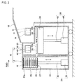
- Fig. 2 illustrates a state where the chip supplying apparatus 10 is set to a mounting machine M. As illustrated in Fig. 2 , in a state where the chip supplying apparatus 10 is set to the mounting machine M, a part in front of the wafer conveyance section 14 is disposed inside the mounting machine M.
- the magazine accommodation portion 12 of the chip supplying apparatus 10 is provided with a housing 20, a magazine 22, and a magazine ascending/descending mechanism 24.
- the housing 20 accommodates the magazine 22 and the magazine ascending/descending mechanism 24.
- a conveying-out port 26 which conveys out a wafer sheet W accommodated in the magazine 22 is formed.
- the wafer sheet W in the embodiment is referred to as a sheet which is made by installing a dicing sheet to which a wafer diced in a desired chip shape is adhered on a wafer holding board having a substantially circular opening at the center thereof.
- an opening/closing lid 20a which is opened and closed by the operator is formed.
- the magazine 22 is provided with a plurality of wafer sheet accommodation portions 28 which accommodate the wafer sheet W.
- the plurality of wafer sheet accommodation portions 28 are layered in a height direction. In each wafer sheet accommodation portion 28, the wafer sheet W is accommodated.
- the magazine 22 is formed in a shape of a prism in which a front surface and a rear surface are opened. The operator of the chip supplying apparatus 10 can open the opening/closing lid 20a of the housing 20 and replenish the wafer sheet W to the wafer sheet accommodation portion 28 by the rear surface of the magazine 22.
- the magazine ascending/descending mechanism 24 includes a ball screw 30, and a motor 32 which rotates the ball screw 30.
- a nut (not illustrated) which is engaged with the ball screw 30 is fixed to the magazine 22.
- the magazine 22 moves in the housing 20 in the up-and-down direction.
- the wafer conveyance section 14 is provided with a stage 34, a stage ascending/descending mechanism 36 which makes the stage 34 ascent and descend, a wafer table 38, and an operation head 40.
- the stage ascending/descending mechanism 36 moves the stage 34 in the up-and-down direction.
- the stage ascending/descending mechanism 36 includes a ball screw 42 and a motor 44 which rotates the ball screw 42.
- a nut (not illustrated) which is engaged with the ball screw 42 is fixed to the stage 34. For this reason, when the ball screw 42 is rotated by the motor 44 , the stage 34 moves in the up-and-down direction.
- the wafer table 38 is supported to be slidable in the front-and-back direction with respect to the stage 34.
- the wafer table 38 can hold the wafer sheet W which is conveyed out from the magazine 22.
- the wafer table 38 can move between a wafer sheet supplying position 38a which is positioned behind the wafer conveyance section 14, and a chip supplying position 38b which is positioned in front of the wafer conveyance section 14.
- the wafer table 38 can rotatably move around a vertical axis with respect to the stage 34.
- a motor not illustrated
- the wafer table 38 can adjust an angle around the vertical axis with respect to the stage 34.
- the operation head 40 is supported to be movable in the front-and-back direction and the right-and-left direction with respect to the stage 34. By driving an actuator (not illustrated), the operation head 40 moves in the front-and-back direction and in the right-and-left direction relative to the stage 34.
- the operation head 40 has a wafer drawing mechanism 46, a suction nozzle 48, and a camera 50 mounted thereon.
- the wafer drawing mechanism 46 draws out the wafer sheet W from the wafer sheet accommodation portion 28 of the magazine accommodation portion 12, and conveys the wafer sheet W to the wafer table 38 which is at the wafer sheet supplying position 38a.
- the suction nozzle 48 can suck a desired chip from the wafer sheet W in a state where the wafer table 38 is at the wafer sheet supplying position 38a.
- the camera 50 images the wafer sheet W which is held by the wafer table 38 from an upper surface in a state where the wafer table 38 is at the wafer sheet supplying position 38a. From the image which is imaged by the camera 50, it is possible to recognize a position and a posture of a chip which is a suction target of the suction nozzle 48 or a suction nozzle N which will be described later, and a state of the wafer table 38.
- the mounting machine M is provided with a mounting head H.
- the mounting head H includes the suction nozzle N and a camera C. The suction nozzle N can suck the desired chip from the wafer sheet W in a state where the wafer table 38 is at the chip supplying position 38b.
- the suction nozzle N is operated based on the position and the posture of the chip which is recognized from the image imaged by the camera 50, but may be operated by recognizing the position and the posture of the chip from an image imaged by the camera C.
- the mounting head H can move in the front-and-back direction and in the right-and-left direction inside the mounting machine M, and can mount the chip which is sucked by the suction nozzle N on the substrate.
- a thrust mechanism which makes the chip easily picked from the dicing sheet by thrusting the wafer sheet W from a lower part of the wafer table 38 when the suction nozzle 48 of the wafer conveyance section 14 and the suction nozzle N of the mounting machine M suck the chip, a pod changer which switches a pod of the thrust mechanism, a nozzle changer which switches the suction nozzle 48, and the like, are mounted.
- the wafer table 38 of the embodiment can hold wafer sheets having various sizes, such as 6 inches, 8 inches, or 12 inches.
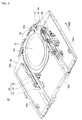
- Fig. 3 illustrates a case where the wafer table 38 holds a 6-inch wafer sheet W.
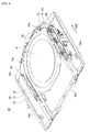
- Fig. 4 illustrates a case where the wafer table 38 holds a 8-inch wafer sheet W.
- Fig. 5 illustrates a case where the wafer table 38 holds a 12-inch wafer sheet W.
- the wafer table 38 is provided with a frame 60, a stopper 62, and a pair of clamp mechanisms 64 and 66.
- the frame 60 is formed in a shape of a rectangular frame having an opening at the center thereof.
- the frame 60 is provided with a front frame plate 60a, a rear frame plate 60b, and a pair of side frame plates 60c and 60d.
- the stopper 62 is provided on an upper surface of a center portion of the front frame plate 60a. As a front end of the wafer sheet W abuts against the stopper 62, the wafer sheet W is positioned in the front-and-back direction with respect to the wafer table 38.
- the clamp mechanisms 64 and 66 are respectively provided with main plates 68 and 70, and sub-plates 72 and 74.
- one clamp mechanism 64 is provided with a side plate 76
- the other clamp mechanism 66 is provided with a side stopper 78.
- the main plates 68 and 70 are supported to be across the opening of the frame 60 in the front-and-back direction by the front frame plate 60a and the rear frame plate 60b. On front sides of the main plates 68 and 70, the main plates 68 and 70 extend to be overlapped with an upper surface of the front frame plate 60a. On rear sides of the main plates 68 and 70, the main plates 68 and 70 extend to be overlapped with an upper surface of the rear frame plate 60b.
- the main plates 68 and 70 are supported to be slidable in the right-and-left direction with respect to the frame 60.
- the main plates 68 and 70 are locked with respect to the frame 60 at a position which is set in advance in accordance with the size of the held wafer sheet W.
- the wafer sheet W which is drawn out by the wafer drawing mechanism 46 is moved forward until the front end abuts against the stopper 62 in a state where both side ends are loaded on upper surfaces of the main plates 68 and 70.
- the side stopper 78 is disposed between the main plate 70 and the sub-plate 74.
- the side stopper 78 is fixed to the main plate 70.
- the side stopper 78 guides forward movement of the wafer sheet W, and positions the side end of the wafer sheet W.
- the side plate 76 is disposed between the main plate 68 and the sub-plate 72.
- the side plate 76 is supported to be slidable in the right-and-left direction with respect to the main plate 68, and slides in the right-and-left direction as an air cylinder is driven.
- the side plate 76 is slid toward the side stopper 78. According to this, the wafer sheet W is held by the side stopper 78 and the side plate 76 from right and left sides, and the wafer sheet W is positioned in the right-and-left direction with respect to the wafer table 38.
- the sub-plates 72 and 74 are supported to be movable in the up-and-down direction with respect to the main plates 68 and 70, and move in the up-and-down direction as the air cylinder is driven.
- the wafer table 38 when the front end of the wafer sheet W abuts against the stopper 62, and further, when the wafer sheet W is held by the side stopper 78 and the side plate 76 from the right and left sides, the sub-plates 72 and 74 are moved toward the main plates 68 and 70. According to this, a side end portion of the wafer sheet W is held by the main plates 68 and 70, and the sub-plates 72 and 74 from upper and lower sides. According to this, the side end portion of the wafer sheet W is clamped, and the wafer sheet W is held by the wafer table 38.
- identification marks 68a and 70a are provided on the upper surfaces of the main plates 68 and 70.
- the image which is imaged by the camera 50 of the wafer conveyance section 14 or by the camera C of the mounting machine M it is possible to recognize the size of the wafer sheet W which can be held by the wafer table 38 by detecting positions of the identification marks 68a and 70a.
- Fig. 6 is a view when the wafer table 38 is viewed from a lower surface side.
- Fig. 7 is an enlarged view along an A-A portion in Fig. 6
- Fig. 8 is an enlarged view along a B-B portion in Fig. 6 .
- a front block 80 which abuts against the rear surface of the front frame plate 60a is provided in front of the lower surface side of the main plate 68.
- the front block 80 is fixed to the main plate 68.
- an engaging claw 84 which is engaged with an engaging groove 82 formed on the lower surface side of the front frame plate 60a is formed.
- the engaging claw 84 is formed in a trapezoidal shape in which the width narrows as approaching a tip end, and the engaging groove 82 is also formed in a trapezoidal shape in which the width narrows as approaching the inside. According to this, it is possible to easily perform engagement and disengagement of the engaging claw 84 and the engaging groove 82.
- a plurality of engaging grooves 82 are formed at a position corresponding to the size of the wafer sheet W which is held by the wafer table 38.
- a rear block 86 which abuts against the front surface of the rear frame plate 60b, and an intermediate block 90 which is linked to the rear block 86 via a spring 88, are provided behind the lower surface side of the main plate 68.
- the intermediate block 90 is fixed to the main plate 68 at a position between the front block 80 and the rear block 86.
- the rear block 86 is supported to be slidable in the front-and-back direction with respect to the main plate 68.
- a flange 92 which extends to be overlapped with the lower surface of the rear frame plate 60b is formed.
- a positioning pin 96 which is engaged with a positioning groove 94 formed on an outer side of the rear frame plate 60b is fixed to the rear end on the lower surface side of the main plate 68.
- a plurality of positioning grooves 94 are formed at a position corresponding to the size of the wafer sheet W which is held by the wafer table 38.
- the position where the positioning groove 94 is formed on the rear frame plate 60b, and the position where the engaging groove 82 is formed on the front frame plate 60a, correspond to each other.
- the spring 88 is compressed, and an elastic restoring force in a direction in which the rear block 86 and the intermediate block 90 are separated from each other acts on the rear block 86 and the intermediate block 90.
- the rear block 86 is pressed against the front surface of the rear frame plate 60b, and the front block 80 is pressed against the rear surface of the front frame plate 60a.
- the engaging claw 84 is reliably engaged with the engaging groove 82, the positioning pin 96 is reliably engaged with the positioning groove 94, and the clamp mechanism 64 is locked with respect to the frame 60.
- the clamp mechanism 64 When the clamp mechanism 64 is slid in the right-and-left direction with respect to the frame 60, first, the operator grasps the main plate 68, and pulls down the main plate 68 rearward with respect to the frame 60. Accordingly, the spring 88 is compressed, the entire main plate 68 slides rearward, the engaging claw 84 of the front block 80 is detached from the engaging groove 82, and the positioning pin 96 is detached from the positioning groove 94. While maintaining this state, the operator slides the main plate 68 in the right-and-left direction with respect to the frame 60.
- a rattling preventative plate 98 is provided on the lower surface side of the rear frame plate 60b.
- the rattling preventative plate 98 is supported to be slightly (specifically, within a range which is less than the width of the positioning groove 94) slidable in the right-and-left direction, with respect to the rear frame plate 60b.
- a guide groove 100 which has substantially the same shape as that of the positioning groove 94 is formed.
- the rattling preventative plate 98 is connected to a block 104 which is fixed to the rear frame plate 60b via a spring 102.
- the spring 102 is attached in a state of being compressed, and biases the rattling preventative plate 98 toward the outer side in the right-and-left direction.
- the positioning pin 96 is engaged with the positioning groove 94, the positioning pin 96 is pressed while abutting against the guide groove 100, and the rattling preventative plate 98 slides on an inner side in the right-and-left direction against the bias from the spring 102.
- the positioning pin 96 is depressed toward the outer side in the right-and-left direction with respect to the positioning groove 94. According to this, the rattling of the positioning pin 96 in the positioning groove 94 is prevented.
- the operator without using a tool, the operator can change the position of the clamp mechanism in the right-and-left direction.
- An operation of changing the size of the wafer table 38 can be extremely easily performed.
- any size of the wafer sheet W positioning is also performed by considering the center of the front end as a reference, with respect to the wafer table 38. Accordingly, it is possible to hold any size of the wafer sheet W at a position which is the nearest to the mounting machine M. It is possible to reduce a movement distance of the mounting head H of the mounting machine M.
Landscapes
- Engineering & Computer Science (AREA)
- Robotics (AREA)
- Mechanical Engineering (AREA)
- Container, Conveyance, Adherence, Positioning, Of Wafer (AREA)
- Die Bonding (AREA)
Abstract
Description
- The present disclosure relates to a chip supplying apparatus which supplies a chip to a mounting machine which mounts the chip on a substrate.
-
JP-A-2010-268015 - In a chip supplying apparatus, there is a case where a user desires to supply a chip from wafers having different sizes from each other. In a chip supplying apparatus in the related art, even when the sizes of the wafers are different from each other, by setting outer shapes of all of wafer holding boards to be the same tray shape, it is possible to hold wafer sheets by the same wafer table. In the chip supplying apparatus in the related art, when the outer shapes of the wafer holding boards are different from each other, and thus, when the sizes of the wafer sheets are different from each other, it is not possible to hold the wafer sheets by the same wafer table. A technology, in which the wafer sheets can be held by the same wafer table even when the sizes of the wafer sheets are different from each other, is expected.
- In this specification, a chip supplying apparatus which supplies a chip to a mounting machine which mounts the chip on a substrate is disclosed. The chip supplying apparatus is provided with a wafer table which holds a wafer sheet at a position where an operation head of the mounting machine can receive the chip. In the chip supplying apparatus, the wafer table is provided with a frame, a stopper which is fixed to the center of a front portion of the frame and abuts against a front end of the wafer sheet, and a pair of clamp mechanisms which is supported by the frame and which clamps both side ends of the wafer sheet. In the chip supplying apparatus, a position of the pair of clamp mechanisms in a right-and-left direction with respect to the frame can be changed in multiple steps.
- In the above-described chip supplying apparatus, as the front end of the wafer sheet abuts against the stopper and both side ends of the wafer sheet are clamped by the pair of clamp mechanisms, the wafer sheet is held being positioned in a front-and-back direction and in a right-and-left direction with respect to the wafer table. In the above-described chip supplying apparatus, by changing the position of the pair of the clamp mechanisms in the right-and-left direction with respect to the frame, it is possible to hold the wafer sheets having different sizes from each other by the same wafer table.
-
- [
Fig. 1] Fig. 1 is a view illustrating an external appearance of achip supplying apparatus 10. - [
Fig. 2] Fig. 2 is a cross-sectional view when a state where thechip supplying apparatus 10 is set to a mounting machine M is viewed from a side. - [
Fig. 3] Fig. 3 is a view illustrating a state where a wafer table 38 holds a 6-inch wafer sheet W. - [
Fig. 4] Fig. 4 is a view illustrating a state where the wafer table 38 holds an 8-inch wafer sheet W. - [
Fig. 5] Fig. 5 is a view illustrating a state where the wafer table 38 holds a 12-inch wafer sheet W. - [
Fig. 6] Fig. 6 is a view when the wafer table 38 is viewed from a lower surface side. - [
Fig. 7] Fig. 7 is a detail enlarged view along A-A inFig. 6 . - [
Fig. 8] Fig. 8 is a detail enlarged view along B-B inFig. 6 . - The above-described chip supplying apparatus can be configured so that a frame is provided with a front frame plate, a rear frame plate, and a side frame plate, a clamp mechanism is supported by the front frame plate and the rear frame plate, a front engaging portion is formed in the vicinity of a front end of the clamp mechanism, a rear engaging portion is formed in the vicinity of a rear end of the clamp mechanism, a plurality of front engaged portions which can be engaged with the front engaging portion are formed on the front frame plate, and a plurality of rear engaged portions that can be engaged with the rear engaging portion are formed on the rear frame plate at a position corresponding to a position of the front engaged portion.
- According to the above-described chip supplying apparatus, by a simple configuration, it is possible to change the position of a pair of clamp mechanisms in a right-and-left direction with respect to the frame in multiple stages.
- The above-described chip supplying apparatus can be configured so that the clamp mechanism is provided with a main plate, a front block which abuts against a rear surface of the front frame plate, a rear block which abuts against a front surface of the rear frame plate, and an intermediate block which is disposed between the front block and the rear block and is fixed to the main plate, one of the front block and the rear block is supported to be slidable in a front-and-back direction with respect to the main plate, and is connected to the intermediate block via an elastic body, the other one of the front block and the rear block is fixed to the main plate, and engagement between the front engaging portion and the front engaged portion is released and an engagement between the rear engaging portion and the rear engaged portion is released by moving the main plate with respect to the frame in a direction in which the elastic body is compressed.
- In the above-described chip supplying apparatus, as an operator grasps the main plate and moves the main plate with respect to the frame in the direction in which the elastic body is compressed, the engagement between the front engaging portion and the front engaged portion is released, and the engagement between the rear engaging portion and the rear engaged portion is released. In this state, as the operator moves the main plate in the right-and-left direction with respect to the frame, it is possible to lock the clamp mechanism at a different position. Without using a tool, with a simple operation, it is possible to change the size of a wafer table.
- The above-described chip supplying apparatus can be configured so that a rattling preventative plate which is supported by the frame via the elastic body is provided in at least one of the front engaged portion and the rear engaged portion.
- According to the above-described chip supplying apparatus, it is possible to prevent rattling between an engaging portion and an engaged portion at a location where the rattling preventative plate is provided.
- The above-described chip supplying apparatus can be configured so that an identification mark is provided on an upper surface of the main plate.
- According to the above-described chip supplying apparatus, by imaging the identification mark by using a camera for imaging a wafer sheet and by detecting a position thereof by image processing, it is possible to recognize the position of the clamp mechanism in the right-and-left direction with respect to the frame.
- A
chip supplying apparatus 10 illustrated inFig. 1 supplies a chip to a mounting machine. The mounting machine mounts the chip which is supplied from thechip supplying apparatus 10 on a substrate which is conveyed in from a production device on an upstream side, and conveys out the substrate on which the chip is mounted to a production device on a downstream side. Thechip supplying apparatus 10 is provided with amagazine accommodation portion 12 and awafer conveyance section 14. In addition, hereinafter, in a state where thechip supplying apparatus 10 is set to the mounting machine, a direction in which the mounting machine is positioned when viewed from thechip supplying apparatus 10 is referred to as a front direction, and an opposite direction thereof is a rear direction. In addition, hereinafter, a right-and-left direction and an up-and-down direction mean a right-and-left direction and an up-and-down direction in a case where a direction in which the mounting machine is positioned is considered as a front direction when viewed from thechip supplying apparatus 10. -
Fig. 2 illustrates a state where thechip supplying apparatus 10 is set to a mounting machine M. As illustrated inFig. 2 , in a state where thechip supplying apparatus 10 is set to the mounting machine M, a part in front of thewafer conveyance section 14 is disposed inside the mounting machine M. - The
magazine accommodation portion 12 of thechip supplying apparatus 10 is provided with ahousing 20, a magazine 22, and a magazine ascending/descendingmechanism 24. - The
housing 20 accommodates the magazine 22 and the magazine ascending/descendingmechanism 24. On a front surface of thehousing 20, a conveying-outport 26 which conveys out a wafer sheet W accommodated in the magazine 22 is formed. The wafer sheet W in the embodiment is referred to as a sheet which is made by installing a dicing sheet to which a wafer diced in a desired chip shape is adhered on a wafer holding board having a substantially circular opening at the center thereof. In addition, on a rear surface of thehousing 20, an opening/closing lid 20a which is opened and closed by the operator is formed. - The magazine 22 is provided with a plurality of wafer
sheet accommodation portions 28 which accommodate the wafer sheet W. The plurality of wafersheet accommodation portions 28 are layered in a height direction. In each wafersheet accommodation portion 28, the wafer sheet W is accommodated. The magazine 22 is formed in a shape of a prism in which a front surface and a rear surface are opened. The operator of thechip supplying apparatus 10 can open the opening/closing lid 20a of thehousing 20 and replenish the wafer sheet W to the wafersheet accommodation portion 28 by the rear surface of the magazine 22. - The magazine ascending/descending
mechanism 24 includes aball screw 30, and amotor 32 which rotates theball screw 30. A nut (not illustrated) which is engaged with theball screw 30 is fixed to the magazine 22. For this reason, when theball screw 30 is rotated by themotor 32, the magazine 22 moves in thehousing 20 in the up-and-down direction. By moving the magazine 22 in the up-and-down direction, it is possible to match the arbitrary wafersheet accommodation portion 28 of the magazine 22 to the height of the conveying-outport 26 of thehousing 20. According to this, it is possible to convey out the wafer sheet W to thewafer conveyance section 14 through the conveying-outport 26 from the wafersheet accommodation portion 28. - The
wafer conveyance section 14 is provided with astage 34, a stage ascending/descendingmechanism 36 which makes thestage 34 ascent and descend, a wafer table 38, and anoperation head 40. - The stage ascending/descending
mechanism 36 moves thestage 34 in the up-and-down direction. The stage ascending/descendingmechanism 36 includes aball screw 42 and amotor 44 which rotates theball screw 42. A nut (not illustrated) which is engaged with theball screw 42 is fixed to thestage 34. For this reason, when theball screw 42 is rotated by themotor 44 , thestage 34 moves in the up-and-down direction. - The wafer table 38 is supported to be slidable in the front-and-back direction with respect to the
stage 34. The wafer table 38 can hold the wafer sheet W which is conveyed out from the magazine 22. By driving an actuator (not illustrated), the wafer table 38 can move between a wafersheet supplying position 38a which is positioned behind thewafer conveyance section 14, and achip supplying position 38b which is positioned in front of thewafer conveyance section 14. In addition, the wafer table 38 can rotatably move around a vertical axis with respect to thestage 34. By driving a motor (not illustrated), the wafer table 38 can adjust an angle around the vertical axis with respect to thestage 34. - The
operation head 40 is supported to be movable in the front-and-back direction and the right-and-left direction with respect to thestage 34. By driving an actuator (not illustrated), theoperation head 40 moves in the front-and-back direction and in the right-and-left direction relative to thestage 34. Theoperation head 40 has awafer drawing mechanism 46, asuction nozzle 48, and acamera 50 mounted thereon. Thewafer drawing mechanism 46 draws out the wafer sheet W from the wafersheet accommodation portion 28 of themagazine accommodation portion 12, and conveys the wafer sheet W to the wafer table 38 which is at the wafersheet supplying position 38a. Thesuction nozzle 48 can suck a desired chip from the wafer sheet W in a state where the wafer table 38 is at the wafersheet supplying position 38a. Thecamera 50 images the wafer sheet W which is held by the wafer table 38 from an upper surface in a state where the wafer table 38 is at the wafersheet supplying position 38a. From the image which is imaged by thecamera 50, it is possible to recognize a position and a posture of a chip which is a suction target of thesuction nozzle 48 or a suction nozzle N which will be described later, and a state of the wafer table 38. - Above the
chip supplying position 38b of the wafer table 38, an upper portion of thewafer conveyance section 14 is opened. For this reason, in a state where the wafer table 38 is at thechip supplying position 38b, it is possible to access the wafer sheet W which is held by the wafer table 38 from the mounting machine M. The mounting machine M is provided with a mounting head H. The mounting head H includes the suction nozzle N and a camera C. The suction nozzle N can suck the desired chip from the wafer sheet W in a state where the wafer table 38 is at thechip supplying position 38b. The suction nozzle N is operated based on the position and the posture of the chip which is recognized from the image imaged by thecamera 50, but may be operated by recognizing the position and the posture of the chip from an image imaged by the camera C. The mounting head H can move in the front-and-back direction and in the right-and-left direction inside the mounting machine M, and can mount the chip which is sucked by the suction nozzle N on the substrate. - In addition, on the
stage 34, a thrust mechanism which makes the chip easily picked from the dicing sheet by thrusting the wafer sheet W from a lower part of the wafer table 38 when thesuction nozzle 48 of thewafer conveyance section 14 and the suction nozzle N of the mounting machine M suck the chip, a pod changer which switches a pod of the thrust mechanism, a nozzle changer which switches thesuction nozzle 48, and the like, are mounted. - The wafer table 38 of the embodiment can hold wafer sheets having various sizes, such as 6 inches, 8 inches, or 12 inches.
Fig. 3 illustrates a case where the wafer table 38 holds a 6-inch wafer sheet W.Fig. 4 illustrates a case where the wafer table 38 holds a 8-inch wafer sheet W.Fig. 5 illustrates a case where the wafer table 38 holds a 12-inch wafer sheet W. - As illustrated in
Figs. 3 to 5 , the wafer table 38 is provided with aframe 60, astopper 62, and a pair ofclamp mechanisms - The
frame 60 is formed in a shape of a rectangular frame having an opening at the center thereof. Theframe 60 is provided with afront frame plate 60a, arear frame plate 60b, and a pair ofside frame plates front frame plate 60a, thestopper 62 is provided. As a front end of the wafer sheet W abuts against thestopper 62, the wafer sheet W is positioned in the front-and-back direction with respect to the wafer table 38. - The
clamp mechanisms main plates clamp mechanism 64 is provided with aside plate 76, and theother clamp mechanism 66 is provided with aside stopper 78. - The
main plates frame 60 in the front-and-back direction by thefront frame plate 60a and therear frame plate 60b. On front sides of themain plates main plates front frame plate 60a. On rear sides of themain plates main plates rear frame plate 60b. Themain plates frame 60. Themain plates frame 60 at a position which is set in advance in accordance with the size of the held wafer sheet W. The wafer sheet W which is drawn out by thewafer drawing mechanism 46 is moved forward until the front end abuts against thestopper 62 in a state where both side ends are loaded on upper surfaces of themain plates - The
side stopper 78 is disposed between themain plate 70 and the sub-plate 74. Theside stopper 78 is fixed to themain plate 70. Theside stopper 78 guides forward movement of the wafer sheet W, and positions the side end of the wafer sheet W. Theside plate 76 is disposed between themain plate 68 and the sub-plate 72. Theside plate 76 is supported to be slidable in the right-and-left direction with respect to themain plate 68, and slides in the right-and-left direction as an air cylinder is driven. In the wafer table 38, when the wafer sheet W moves forward on themain plates stopper 62, theside plate 76 is slid toward theside stopper 78. According to this, the wafer sheet W is held by theside stopper 78 and theside plate 76 from right and left sides, and the wafer sheet W is positioned in the right-and-left direction with respect to the wafer table 38. - The sub-plates 72 and 74 are supported to be movable in the up-and-down direction with respect to the
main plates stopper 62, and further, when the wafer sheet W is held by theside stopper 78 and theside plate 76 from the right and left sides, the sub-plates 72 and 74 are moved toward themain plates main plates - In addition, on the upper surfaces of the
main plates camera 50 of thewafer conveyance section 14 or by the camera C of the mounting machine M, it is possible to recognize the size of the wafer sheet W which can be held by the wafer table 38 by detecting positions of the identification marks 68a and 70a. - Hereinafter, with reference to
Figs. 6 to 8 , size changing when the size of the wafer sheet W which is held by the wafer table 38 is changed, will be described with theclamp mechanism 64 as an example. Theclamp mechanism 66 is also similar to theclamp mechanism 64.Fig. 6 is a view when the wafer table 38 is viewed from a lower surface side. In addition,Fig. 7 is an enlarged view along an A-A portion inFig. 6 , andFig. 8 is an enlarged view along a B-B portion inFig. 6 . - As illustrated in
Fig. 7 , in front of the lower surface side of themain plate 68, afront block 80 which abuts against the rear surface of thefront frame plate 60a is provided. Thefront block 80 is fixed to themain plate 68. In thefront block 80, an engagingclaw 84 which is engaged with an engaginggroove 82 formed on the lower surface side of thefront frame plate 60a is formed. The engagingclaw 84 is formed in a trapezoidal shape in which the width narrows as approaching a tip end, and the engaginggroove 82 is also formed in a trapezoidal shape in which the width narrows as approaching the inside. According to this, it is possible to easily perform engagement and disengagement of the engagingclaw 84 and the engaginggroove 82. When the engagingclaw 84 is engaged with the engaginggroove 82, the front side of themain plate 68 is prohibited from moving in the right-and-left direction with respect to thefront frame plate 60a. As illustrated inFig. 7 , a plurality of engaginggrooves 82 are formed at a position corresponding to the size of the wafer sheet W which is held by the wafer table 38. - As illustrated in
Fig. 8 , behind the lower surface side of themain plate 68, arear block 86 which abuts against the front surface of therear frame plate 60b, and anintermediate block 90 which is linked to therear block 86 via a spring 88, are provided. Theintermediate block 90 is fixed to themain plate 68 at a position between thefront block 80 and therear block 86. Therear block 86 is supported to be slidable in the front-and-back direction with respect to themain plate 68. In therear block 86, aflange 92 which extends to be overlapped with the lower surface of therear frame plate 60b is formed. In addition, apositioning pin 96 which is engaged with apositioning groove 94 formed on an outer side of therear frame plate 60b is fixed to the rear end on the lower surface side of themain plate 68. As illustrated inFig. 8 , a plurality ofpositioning grooves 94 are formed at a position corresponding to the size of the wafer sheet W which is held by the wafer table 38. The position where thepositioning groove 94 is formed on therear frame plate 60b, and the position where the engaginggroove 82 is formed on thefront frame plate 60a, correspond to each other. - In a state where the
clamp mechanism 64 is attached to theframe 60, the spring 88 is compressed, and an elastic restoring force in a direction in which therear block 86 and theintermediate block 90 are separated from each other acts on therear block 86 and theintermediate block 90. According to this, therear block 86 is pressed against the front surface of therear frame plate 60b, and thefront block 80 is pressed against the rear surface of thefront frame plate 60a. Accordingly, the engagingclaw 84 is reliably engaged with the engaginggroove 82, thepositioning pin 96 is reliably engaged with thepositioning groove 94, and theclamp mechanism 64 is locked with respect to theframe 60. - When the
clamp mechanism 64 is slid in the right-and-left direction with respect to theframe 60, first, the operator grasps themain plate 68, and pulls down themain plate 68 rearward with respect to theframe 60. Accordingly, the spring 88 is compressed, the entiremain plate 68 slides rearward, the engagingclaw 84 of thefront block 80 is detached from the engaginggroove 82, and thepositioning pin 96 is detached from thepositioning groove 94. While maintaining this state, the operator slides themain plate 68 in the right-and-left direction with respect to theframe 60. When themain plate 68 is moved up to desired positions of the engaginggroove 82 and thepositioning groove 94, and the operator weakens a force of pulling down themain plate 68 rearward, by the elastic restoring force of the spring 88, the engagingclaw 84 of thefront block 80 is engaged with the engaginggroove 82, and thepositioning pin 96 is engaged with thepositioning groove 94. According to this, it is possible to change in a stepwise manner the position of theclamp mechanism 64 in the right-and-left direction with respect to theframe 60. - In addition, on the lower surface side of the
rear frame plate 60b, a rattlingpreventative plate 98 is provided. The rattlingpreventative plate 98 is supported to be slightly (specifically, within a range which is less than the width of the positioning groove 94) slidable in the right-and-left direction, with respect to therear frame plate 60b. In the rattlingpreventative plate 98, aguide groove 100 which has substantially the same shape as that of thepositioning groove 94 is formed. The rattlingpreventative plate 98 is connected to ablock 104 which is fixed to therear frame plate 60b via aspring 102. Thespring 102 is attached in a state of being compressed, and biases the rattlingpreventative plate 98 toward the outer side in the right-and-left direction. When thepositioning pin 96 is engaged with thepositioning groove 94, thepositioning pin 96 is pressed while abutting against theguide groove 100, and the rattlingpreventative plate 98 slides on an inner side in the right-and-left direction against the bias from thespring 102. In a state where thepositioning pin 96 is engaged with thepositioning groove 94, by the rattlingpreventative plate 98 which is biased by thespring 102, thepositioning pin 96 is depressed toward the outer side in the right-and-left direction with respect to thepositioning groove 94. According to this, the rattling of thepositioning pin 96 in thepositioning groove 94 is prevented. - As described above, according to the embodiment, without using a tool, the operator can change the position of the clamp mechanism in the right-and-left direction. An operation of changing the size of the wafer table 38 can be extremely easily performed.
- According to the embodiment, regarding any size of the wafer sheet W, positioning is also performed by considering the center of the front end as a reference, with respect to the wafer table 38. Accordingly, it is possible to hold any size of the wafer sheet W at a position which is the nearest to the mounting machine M. It is possible to reduce a movement distance of the mounting head H of the mounting machine M.
- In addition, by installing wafers having different sizes from each other onto a wafer holding board having the same tray shape as the wafer sheet W, without changing the size of the wafer table 38, a configuration in which the wafers having different sizes from each other are handled can be employed.
- A representative and non-limiting specific example of the present invention is described in detail with reference to the drawings. The detail description simply illustrates the details for realizing a preferable example of the invention for those skilled in the art, and does not limit the range of the present invention. In addition, the disclosed additional characteristics and invention can be used separately or together with other characteristics and inventions in order to provide a more improved chip supplying apparatus.
- In addition, a combination of the characteristics or processes disclosed in the above-described detail description is not necessary when realizing the present invention in a broadest sense, and in particular, the description is only for describing the representative detail example of the present invention. Furthermore, various characteristics of the above-described representative detail example, and various characteristics described in the independent and dependent claims, are not necessarily combined according to the detail example described here or the listed order when providing an additional and useful embodiment of the present invention.
- All of the characteristics described in this specification and/or claims, are characteristics which are disclosed separately and independently from each other as a restriction with respect to a certain item in the initial disclosure and the claims of the application, in addition to the configuration of the characteristics described in the embodiment and/or claims. Furthermore, the description regarding the entire numeral value range and group or aggregation is to disclose an intermediate configuration as a restriction with respect to a certain item in the initial disclosure and the claims of the application.
- Above, detail examples of the present invention are described, but these are merely examples, and the range of the aspects of invention is not limited thereto. In the technology which is described within the range of the aspects of the invention, various modifications and changes of the above-described detail examples are included. Technical elements which are described in this specification and in the drawings achieve technical usefulness by using the examples independently or by combining various examples, and are not limited to the combination of the described aspects of the application. In addition, the technology described in this specification and in the drawings can achieve a plurality of purposes at the same time, and technical usefulness is realized only by achieving one of the purposes.
Claims (5)
- A chip supplying apparatus which supplies a chip to a mounting machine which mounts the chip on a substrate, comprising:a wafer table which holds a wafer sheet at a position where an operation head of the mounting machine can receive the chip,wherein the wafer table includes a frame, a stopper which is fixed to the center of a front portion of the frame and abuts against a front end of the wafer sheet, and a pair of clamp mechanisms which is supported by the frame and which clamps both side ends of the wafer sheet, andwherein a position of the pair of clamp mechanisms in the right-and-left direction with respect to the frame is changed in multiple steps.
- The chip supplying apparatus according to Claim 1,
wherein the frame includes a front frame plate, a rear frame plate, and a pair of side frame plates,
wherein each of the pair of clamp mechanisms is supported by the front frame plate and the rear frame plate,
wherein a front engaging portion is formed in the vicinity of a front end of each of the pair of clamp mechanisms, and a rear engaging portion is formed in the vicinity of a rear end of each of the pair of clamp mechanisms,
wherein a plurality of front engaged portions which are engaged with the front engaging portion are formed on the front frame plate, and
wherein, at a position corresponding to a position of the front engaged portion, a plurality of rear engaged portions which are engaged with the rear engaging portion are formed on the rear frame plate. - The chip supplying apparatus according to Claim 2,
wherein each of the pair of clamp mechanisms includes a main plate, a front block which abuts against a rear surface of the front frame plate, a rear block which abuts against a front surface of the rear frame plate, and an intermediate block which is disposed between the front block and the rear block and fixed to the main plate,
wherein one of the front block and the rear block is supported to be slidable in the front-and-back direction with respect to the main plate, and is connected to the intermediate block via an elastic body,
wherein the other one of the front block and the rear block is fixed to the main plate, and
wherein, by moving the main plate with respect to the frame in a direction in which the elastic body is compressed, the engagement between the front engaging portion and the front engaged portion, and the engagement between the rear engaging portion and the rear engaged portion, are released. - The chip supplying apparatus according to Claim 3,
wherein, in at least one of the front engaged portion and the rear engaged portion, a rattling preventative plate which is supported by the frame via the elastic body is provided. - The chip supplying apparatus according to any one of Claims 1 to 4,
wherein, on an upper surface of the main plate, an identification mark is provided.
Applications Claiming Priority (1)
| Application Number | Priority Date | Filing Date | Title |
|---|---|---|---|
| PCT/JP2012/078873 WO2014073057A1 (en) | 2012-11-07 | 2012-11-07 | Chip supply apparatus |
Publications (3)
| Publication Number | Publication Date |
|---|---|
| EP2919260A1 true EP2919260A1 (en) | 2015-09-16 |
| EP2919260A4 EP2919260A4 (en) | 2015-10-28 |
| EP2919260B1 EP2919260B1 (en) | 2016-08-03 |
Family
ID=50684195
Family Applications (1)
| Application Number | Title | Priority Date | Filing Date |
|---|---|---|---|
| EP12887866.7A Active EP2919260B1 (en) | 2012-11-07 | 2012-11-07 | Chip supply apparatus |
Country Status (5)
| Country | Link |
|---|---|
| US (1) | US9520317B2 (en) |
| EP (1) | EP2919260B1 (en) |
| JP (1) | JP5974109B2 (en) |
| CN (1) | CN104769706B (en) |
| WO (1) | WO2014073057A1 (en) |
Families Citing this family (9)
| Publication number | Priority date | Publication date | Assignee | Title |
|---|---|---|---|---|
| US9887111B2 (en) * | 2014-03-24 | 2018-02-06 | Fuji Machine Mfg. Co., Ltd. | Die mounting system and die mounting method |
| US9352471B1 (en) * | 2015-01-21 | 2016-05-31 | Applied Materials, Inc. | Substrate gripper apparatus and methods |
| TW201714718A (en) * | 2015-10-21 | 2017-05-01 | 億力鑫系統科技股份有限公司 | Centering device and processing device having the same |
| CN106611737B (en) * | 2015-10-26 | 2020-11-10 | 北京北方华创微电子装备有限公司 | Ring pressing device |
| JP2017112227A (en) * | 2015-12-16 | 2017-06-22 | 株式会社ディスコ | Processing equipment |
| CN110164813B (en) * | 2019-04-22 | 2021-01-26 | 湖北华威科智能股份有限公司 | Wafer clamping and feeding device suitable for multiple dimensions |
| KR102822419B1 (en) * | 2020-12-08 | 2025-06-18 | 에스케이하이닉스 주식회사 | Semiconductor manufacturing equipment, method of reading position of carrier and method of attaching semiconductor die on carrier using semiconductor manufacturing equipment |
| CN112687581B (en) * | 2020-12-10 | 2024-02-02 | 宁波市甬粤芯微电子科技有限公司 | Chip photoetching processing equipment and chip processing technology |
| CN112781635A (en) * | 2021-02-02 | 2021-05-11 | 苏州矩浪科技有限公司 | A wafer fixing mechanism |
Family Cites Families (14)
| Publication number | Priority date | Publication date | Assignee | Title |
|---|---|---|---|---|
| US5046909A (en) * | 1989-06-29 | 1991-09-10 | Applied Materials, Inc. | Method and apparatus for handling semiconductor wafers |
| JP3442849B2 (en) * | 1994-04-06 | 2003-09-02 | 株式会社東芝 | Method for manufacturing semiconductor device |
| IL119213A (en) * | 1996-09-06 | 2000-08-31 | Orbot Instr Ltd | Universal chuck for holding plates of various sizes |
| US6986636B2 (en) * | 2000-06-09 | 2006-01-17 | Brooks Automation, Inc. | Device for positioning disk-shaped objects |
| CN100337164C (en) * | 2002-12-06 | 2007-09-12 | 精工爱普生株式会社 | Imaging device |
| JP4085995B2 (en) * | 2004-03-16 | 2008-05-14 | 松下電器産業株式会社 | Rotary table mechanism |
| US7886449B2 (en) * | 2007-02-20 | 2011-02-15 | Electro Scientific Industries, Inc. | Flexure guide bearing for short stroke stage |
| US8296937B2 (en) * | 2008-08-19 | 2012-10-30 | Silverbrook Research Pty Ltd | Wafer positioning system |
| TW201013835A (en) * | 2008-09-26 | 2010-04-01 | Gudeng Prec Industral Co Ltd | Sheet clamping apparatus |
| JP2011211055A (en) * | 2010-03-30 | 2011-10-20 | Lintec Corp | Expand device |
| JP5635835B2 (en) * | 2010-08-18 | 2014-12-03 | 富士機械製造株式会社 | Wafer supply device and chip bonding device |
| JP5410388B2 (en) * | 2010-09-02 | 2014-02-05 | 富士機械製造株式会社 | Chip holding device, chip supply device and chip mounting machine |
| JP5582646B2 (en) * | 2010-11-04 | 2014-09-03 | 富士機械製造株式会社 | Waste tape recovery device for component mounters |
| US8567837B2 (en) * | 2010-11-24 | 2013-10-29 | Taiwan Semiconductor Manufacturing Company, Ltd. | Reconfigurable guide pin design for centering wafers having different sizes |
-
2012
- 2012-11-07 US US14/441,305 patent/US9520317B2/en active Active
- 2012-11-07 CN CN201280076903.7A patent/CN104769706B/en active Active
- 2012-11-07 EP EP12887866.7A patent/EP2919260B1/en active Active
- 2012-11-07 JP JP2014545490A patent/JP5974109B2/en active Active
- 2012-11-07 WO PCT/JP2012/078873 patent/WO2014073057A1/en not_active Ceased
Also Published As
| Publication number | Publication date |
|---|---|
| EP2919260B1 (en) | 2016-08-03 |
| JP5974109B2 (en) | 2016-08-23 |
| CN104769706B (en) | 2017-12-05 |
| CN104769706A (en) | 2015-07-08 |
| US9520317B2 (en) | 2016-12-13 |
| EP2919260A4 (en) | 2015-10-28 |
| WO2014073057A1 (en) | 2014-05-15 |
| JPWO2014073057A1 (en) | 2016-09-08 |
| US20150287627A1 (en) | 2015-10-08 |
Similar Documents
| Publication | Publication Date | Title |
|---|---|---|
| US9520317B2 (en) | Chip supplying apparatus | |
| JP6204997B2 (en) | Suction nozzle for mounting electronic components | |
| US10568250B2 (en) | Component mounting device and method of mounting component | |
| JPWO2015181910A1 (en) | Parts mounting machine | |
| JP6259462B2 (en) | Chuck device and component mounting machine | |
| US11202374B2 (en) | Method of mounting component | |
| JP6230694B2 (en) | Panel device and work machine | |
| JP6074436B2 (en) | Parts supply device | |
| JPWO2005081611A1 (en) | Support pin gripping device and substrate supporting device | |
| JP6262243B2 (en) | Component mounting device | |
| JP6110414B2 (en) | Die supply device | |
| US9781870B2 (en) | Component supply device | |
| JP6590364B2 (en) | Component mounting device | |
| JP4851314B2 (en) | Printed circuit board holding device | |
| KR101779585B1 (en) | The print table driving device | |
| JP4349125B2 (en) | Electronic component mounting device | |
| JP2009200201A (en) | Chip supply pallet | |
| JP5086869B2 (en) | Electronic component mounting device | |
| CN122071089A (en) | Substrate processing apparatus and substrate processing method |
Legal Events
| Date | Code | Title | Description |
|---|---|---|---|
| PUAI | Public reference made under article 153(3) epc to a published international application that has entered the european phase |
Free format text: ORIGINAL CODE: 0009012 |
|
| 17P | Request for examination filed |
Effective date: 20150507 |
|
| AK | Designated contracting states |
Kind code of ref document: A1 Designated state(s): AL AT BE BG CH CY CZ DE DK EE ES FI FR GB GR HR HU IE IS IT LI LT LU LV MC MK MT NL NO PL PT RO RS SE SI SK SM TR |
|
| AX | Request for extension of the european patent |
Extension state: BA ME |
|
| RA4 | Supplementary search report drawn up and despatched (corrected) |
Effective date: 20150924 |
|
| RIC1 | Information provided on ipc code assigned before grant |
Ipc: H01L 21/52 20060101AFI20150918BHEP |
|
| DAX | Request for extension of the european patent (deleted) | ||
| GRAP | Despatch of communication of intention to grant a patent |
Free format text: ORIGINAL CODE: EPIDOSNIGR1 |
|
| INTG | Intention to grant announced |
Effective date: 20160314 |
|
| GRAS | Grant fee paid |
Free format text: ORIGINAL CODE: EPIDOSNIGR3 |
|
| GRAA | (expected) grant |
Free format text: ORIGINAL CODE: 0009210 |
|
| AK | Designated contracting states |
Kind code of ref document: B1 Designated state(s): AL AT BE BG CH CY CZ DE DK EE ES FI FR GB GR HR HU IE IS IT LI LT LU LV MC MK MT NL NO PL PT RO RS SE SI SK SM TR |
|
| REG | Reference to a national code |
Ref country code: GB Ref legal event code: FG4D |
|
| REG | Reference to a national code |
Ref country code: CH Ref legal event code: NV Representative=s name: BOVARD AG, CH Ref country code: CH Ref legal event code: EP Ref country code: AT Ref legal event code: REF Ref document number: 817842 Country of ref document: AT Kind code of ref document: T Effective date: 20160815 |
|
| REG | Reference to a national code |
Ref country code: IE Ref legal event code: FG4D |
|
| REG | Reference to a national code |
Ref country code: DE Ref legal event code: R096 Ref document number: 602012021336 Country of ref document: DE |
|
| REG | Reference to a national code |
Ref country code: NL Ref legal event code: MP Effective date: 20160803 |
|
| REG | Reference to a national code |
Ref country code: LT Ref legal event code: MG4D |
|
| PG25 | Lapsed in a contracting state [announced via postgrant information from national office to epo] |
Ref country code: LT Free format text: LAPSE BECAUSE OF FAILURE TO SUBMIT A TRANSLATION OF THE DESCRIPTION OR TO PAY THE FEE WITHIN THE PRESCRIBED TIME-LIMIT Effective date: 20160803 Ref country code: FI Free format text: LAPSE BECAUSE OF FAILURE TO SUBMIT A TRANSLATION OF THE DESCRIPTION OR TO PAY THE FEE WITHIN THE PRESCRIBED TIME-LIMIT Effective date: 20160803 Ref country code: IT Free format text: LAPSE BECAUSE OF FAILURE TO SUBMIT A TRANSLATION OF THE DESCRIPTION OR TO PAY THE FEE WITHIN THE PRESCRIBED TIME-LIMIT Effective date: 20160803 Ref country code: NO Free format text: LAPSE BECAUSE OF FAILURE TO SUBMIT A TRANSLATION OF THE DESCRIPTION OR TO PAY THE FEE WITHIN THE PRESCRIBED TIME-LIMIT Effective date: 20161103 Ref country code: NL Free format text: LAPSE BECAUSE OF FAILURE TO SUBMIT A TRANSLATION OF THE DESCRIPTION OR TO PAY THE FEE WITHIN THE PRESCRIBED TIME-LIMIT Effective date: 20160803 Ref country code: RS Free format text: LAPSE BECAUSE OF FAILURE TO SUBMIT A TRANSLATION OF THE DESCRIPTION OR TO PAY THE FEE WITHIN THE PRESCRIBED TIME-LIMIT Effective date: 20160803 Ref country code: HR Free format text: LAPSE BECAUSE OF FAILURE TO SUBMIT A TRANSLATION OF THE DESCRIPTION OR TO PAY THE FEE WITHIN THE PRESCRIBED TIME-LIMIT Effective date: 20160803 Ref country code: IS Free format text: LAPSE BECAUSE OF FAILURE TO SUBMIT A TRANSLATION OF THE DESCRIPTION OR TO PAY THE FEE WITHIN THE PRESCRIBED TIME-LIMIT Effective date: 20161203 |
|
| PG25 | Lapsed in a contracting state [announced via postgrant information from national office to epo] |
Ref country code: BE Free format text: LAPSE BECAUSE OF NON-PAYMENT OF DUE FEES Effective date: 20161130 Ref country code: SE Free format text: LAPSE BECAUSE OF FAILURE TO SUBMIT A TRANSLATION OF THE DESCRIPTION OR TO PAY THE FEE WITHIN THE PRESCRIBED TIME-LIMIT Effective date: 20160803 Ref country code: ES Free format text: LAPSE BECAUSE OF FAILURE TO SUBMIT A TRANSLATION OF THE DESCRIPTION OR TO PAY THE FEE WITHIN THE PRESCRIBED TIME-LIMIT Effective date: 20160803 Ref country code: PL Free format text: LAPSE BECAUSE OF FAILURE TO SUBMIT A TRANSLATION OF THE DESCRIPTION OR TO PAY THE FEE WITHIN THE PRESCRIBED TIME-LIMIT Effective date: 20160803 Ref country code: GR Free format text: LAPSE BECAUSE OF FAILURE TO SUBMIT A TRANSLATION OF THE DESCRIPTION OR TO PAY THE FEE WITHIN THE PRESCRIBED TIME-LIMIT Effective date: 20161104 Ref country code: PT Free format text: LAPSE BECAUSE OF FAILURE TO SUBMIT A TRANSLATION OF THE DESCRIPTION OR TO PAY THE FEE WITHIN THE PRESCRIBED TIME-LIMIT Effective date: 20161205 Ref country code: LV Free format text: LAPSE BECAUSE OF FAILURE TO SUBMIT A TRANSLATION OF THE DESCRIPTION OR TO PAY THE FEE WITHIN THE PRESCRIBED TIME-LIMIT Effective date: 20160803 |
|
| PG25 | Lapsed in a contracting state [announced via postgrant information from national office to epo] |
Ref country code: RO Free format text: LAPSE BECAUSE OF FAILURE TO SUBMIT A TRANSLATION OF THE DESCRIPTION OR TO PAY THE FEE WITHIN THE PRESCRIBED TIME-LIMIT Effective date: 20160803 Ref country code: EE Free format text: LAPSE BECAUSE OF FAILURE TO SUBMIT A TRANSLATION OF THE DESCRIPTION OR TO PAY THE FEE WITHIN THE PRESCRIBED TIME-LIMIT Effective date: 20160803 |
|
| REG | Reference to a national code |
Ref country code: DE Ref legal event code: R097 Ref document number: 602012021336 Country of ref document: DE |
|
| PG25 | Lapsed in a contracting state [announced via postgrant information from national office to epo] |
Ref country code: CZ Free format text: LAPSE BECAUSE OF FAILURE TO SUBMIT A TRANSLATION OF THE DESCRIPTION OR TO PAY THE FEE WITHIN THE PRESCRIBED TIME-LIMIT Effective date: 20160803 Ref country code: BE Free format text: LAPSE BECAUSE OF FAILURE TO SUBMIT A TRANSLATION OF THE DESCRIPTION OR TO PAY THE FEE WITHIN THE PRESCRIBED TIME-LIMIT Effective date: 20160803 Ref country code: SK Free format text: LAPSE BECAUSE OF FAILURE TO SUBMIT A TRANSLATION OF THE DESCRIPTION OR TO PAY THE FEE WITHIN THE PRESCRIBED TIME-LIMIT Effective date: 20160803 Ref country code: BG Free format text: LAPSE BECAUSE OF FAILURE TO SUBMIT A TRANSLATION OF THE DESCRIPTION OR TO PAY THE FEE WITHIN THE PRESCRIBED TIME-LIMIT Effective date: 20161103 Ref country code: DK Free format text: LAPSE BECAUSE OF FAILURE TO SUBMIT A TRANSLATION OF THE DESCRIPTION OR TO PAY THE FEE WITHIN THE PRESCRIBED TIME-LIMIT Effective date: 20160803 Ref country code: SM Free format text: LAPSE BECAUSE OF FAILURE TO SUBMIT A TRANSLATION OF THE DESCRIPTION OR TO PAY THE FEE WITHIN THE PRESCRIBED TIME-LIMIT Effective date: 20160803 |
|
| PLBE | No opposition filed within time limit |
Free format text: ORIGINAL CODE: 0009261 |
|
| STAA | Information on the status of an ep patent application or granted ep patent |
Free format text: STATUS: NO OPPOSITION FILED WITHIN TIME LIMIT |
|
| 26N | No opposition filed |
Effective date: 20170504 |
|
| GBPC | Gb: european patent ceased through non-payment of renewal fee |
Effective date: 20161107 |
|
| REG | Reference to a national code |
Ref country code: IE Ref legal event code: MM4A |
|
| REG | Reference to a national code |
Ref country code: FR Ref legal event code: ST Effective date: 20170731 |
|
| PG25 | Lapsed in a contracting state [announced via postgrant information from national office to epo] |
Ref country code: SI Free format text: LAPSE BECAUSE OF FAILURE TO SUBMIT A TRANSLATION OF THE DESCRIPTION OR TO PAY THE FEE WITHIN THE PRESCRIBED TIME-LIMIT Effective date: 20160803 |
|
| PG25 | Lapsed in a contracting state [announced via postgrant information from national office to epo] |
Ref country code: LU Free format text: LAPSE BECAUSE OF NON-PAYMENT OF DUE FEES Effective date: 20161130 |
|
| PG25 | Lapsed in a contracting state [announced via postgrant information from national office to epo] |
Ref country code: FR Free format text: LAPSE BECAUSE OF NON-PAYMENT OF DUE FEES Effective date: 20161130 |
|
| PG25 | Lapsed in a contracting state [announced via postgrant information from national office to epo] |
Ref country code: GB Free format text: LAPSE BECAUSE OF NON-PAYMENT OF DUE FEES Effective date: 20161107 Ref country code: IE Free format text: LAPSE BECAUSE OF NON-PAYMENT OF DUE FEES Effective date: 20161107 |
|
| PG25 | Lapsed in a contracting state [announced via postgrant information from national office to epo] |
Ref country code: HU Free format text: LAPSE BECAUSE OF FAILURE TO SUBMIT A TRANSLATION OF THE DESCRIPTION OR TO PAY THE FEE WITHIN THE PRESCRIBED TIME-LIMIT; INVALID AB INITIO Effective date: 20121107 |
|
| PG25 | Lapsed in a contracting state [announced via postgrant information from national office to epo] |
Ref country code: MC Free format text: LAPSE BECAUSE OF FAILURE TO SUBMIT A TRANSLATION OF THE DESCRIPTION OR TO PAY THE FEE WITHIN THE PRESCRIBED TIME-LIMIT Effective date: 20160803 Ref country code: MK Free format text: LAPSE BECAUSE OF FAILURE TO SUBMIT A TRANSLATION OF THE DESCRIPTION OR TO PAY THE FEE WITHIN THE PRESCRIBED TIME-LIMIT Effective date: 20160803 Ref country code: CY Free format text: LAPSE BECAUSE OF FAILURE TO SUBMIT A TRANSLATION OF THE DESCRIPTION OR TO PAY THE FEE WITHIN THE PRESCRIBED TIME-LIMIT Effective date: 20160803 |
|
| REG | Reference to a national code |
Ref country code: DE Ref legal event code: R082 Ref document number: 602012021336 Country of ref document: DE Representative=s name: GRUENECKER PATENT- UND RECHTSANWAELTE PARTG MB, DE Ref country code: DE Ref legal event code: R081 Ref document number: 602012021336 Country of ref document: DE Owner name: FUJI CORPORATION, CHIRYU-SHI, JP Free format text: FORMER OWNER: FUJI MACHINE MFG. CO., LTD., CHIRYU-SHI, AICHI-KEN, JP |
|
| PG25 | Lapsed in a contracting state [announced via postgrant information from national office to epo] |
Ref country code: MT Free format text: LAPSE BECAUSE OF NON-PAYMENT OF DUE FEES Effective date: 20161107 |
|
| REG | Reference to a national code |
Ref country code: CH Ref legal event code: PFA Owner name: FUJI CORPORATION, JP Free format text: FORMER OWNER: FUJI MACHINE MFG. CO., LTD., JP |
|
| PG25 | Lapsed in a contracting state [announced via postgrant information from national office to epo] |
Ref country code: AL Free format text: LAPSE BECAUSE OF FAILURE TO SUBMIT A TRANSLATION OF THE DESCRIPTION OR TO PAY THE FEE WITHIN THE PRESCRIBED TIME-LIMIT Effective date: 20160803 Ref country code: TR Free format text: LAPSE BECAUSE OF FAILURE TO SUBMIT A TRANSLATION OF THE DESCRIPTION OR TO PAY THE FEE WITHIN THE PRESCRIBED TIME-LIMIT Effective date: 20160803 |
|
| REG | Reference to a national code |
Ref country code: AT Ref legal event code: HC Ref document number: 817842 Country of ref document: AT Kind code of ref document: T Owner name: FUJI CORPORATION, JP Effective date: 20190320 Ref country code: AT Ref legal event code: UEP Ref document number: 817842 Country of ref document: AT Kind code of ref document: T Effective date: 20160803 |
|
| P01 | Opt-out of the competence of the unified patent court (upc) registered |
Effective date: 20230328 |
|
| REG | Reference to a national code |
Ref country code: DE Ref legal event code: R079 Ref document number: 602012021336 Country of ref document: DE Free format text: PREVIOUS MAIN CLASS: H01L0021520000 Ipc: H10W0076010000 |
|
| REG | Reference to a national code |
Ref country code: CH Ref legal event code: U11 Free format text: ST27 STATUS EVENT CODE: U-0-0-U10-U11 (AS PROVIDED BY THE NATIONAL OFFICE) Effective date: 20251201 |
|
| PGFP | Annual fee paid to national office [announced via postgrant information from national office to epo] |
Ref country code: DE Payment date: 20250930 Year of fee payment: 14 |
|
| PGFP | Annual fee paid to national office [announced via postgrant information from national office to epo] |
Ref country code: AT Payment date: 20251027 Year of fee payment: 14 |
|
| PGFP | Annual fee paid to national office [announced via postgrant information from national office to epo] |
Ref country code: CH Payment date: 20251201 Year of fee payment: 14 |