EP2916232A1 - Electronic control device for vehicle - Google Patents
Electronic control device for vehicle Download PDFInfo
- Publication number
- EP2916232A1 EP2916232A1 EP13852259.4A EP13852259A EP2916232A1 EP 2916232 A1 EP2916232 A1 EP 2916232A1 EP 13852259 A EP13852259 A EP 13852259A EP 2916232 A1 EP2916232 A1 EP 2916232A1
- Authority
- EP
- European Patent Office
- Prior art keywords
- data
- block
- learning
- learning values
- flash memory
- Prior art date
- Legal status (The legal status is an assumption and is not a legal conclusion. Google has not performed a legal analysis and makes no representation as to the accuracy of the status listed.)
- Granted
Links
Images


Classifications
-
- G—PHYSICS
- G06—COMPUTING OR CALCULATING; COUNTING
- G06F—ELECTRIC DIGITAL DATA PROCESSING
- G06F12/00—Accessing, addressing or allocating within memory systems or architectures
- G06F12/02—Addressing or allocation; Relocation
- G06F12/0223—User address space allocation, e.g. contiguous or non contiguous base addressing
- G06F12/023—Free address space management
- G06F12/0238—Memory management in non-volatile memory, e.g. resistive RAM or ferroelectric memory
- G06F12/0246—Memory management in non-volatile memory, e.g. resistive RAM or ferroelectric memory in block erasable memory, e.g. flash memory
-
- G—PHYSICS
- G05—CONTROLLING; REGULATING
- G05B—CONTROL OR REGULATING SYSTEMS IN GENERAL; FUNCTIONAL ELEMENTS OF SUCH SYSTEMS; MONITORING OR TESTING ARRANGEMENTS FOR SUCH SYSTEMS OR ELEMENTS
- G05B2219/00—Program-control systems
- G05B2219/20—Pc systems
- G05B2219/26—Pc applications
- G05B2219/2637—Vehicle, car, auto, wheelchair
-
- G—PHYSICS
- G06—COMPUTING OR CALCULATING; COUNTING
- G06F—ELECTRIC DIGITAL DATA PROCESSING
- G06F2212/00—Indexing scheme relating to accessing, addressing or allocation within memory systems or architectures
- G06F2212/72—Details relating to flash memory management
- G06F2212/7202—Allocation control and policies
-
- G—PHYSICS
- G06—COMPUTING OR CALCULATING; COUNTING
- G06F—ELECTRIC DIGITAL DATA PROCESSING
- G06F2212/00—Indexing scheme relating to accessing, addressing or allocation within memory systems or architectures
- G06F2212/72—Details relating to flash memory management
- G06F2212/7204—Capacity control, e.g. partitioning, end-of-life degradation
Definitions
- the present invention relates to an electronic control device for a vehicle.
- An electronic control device mounted on a vehicle can learn and update control parameters to be used for engine control. By learning the control parameters, cleaning of exhaust gas and improvement in fuel economy can be achieved.
- a flash memory is used for a device that stores therein the latest learning values of the parameters to realize cost reduction.
- learning values of a plurality of parameters are temporarily stored in a first memory area of the flash memory and, when an update condition of the learning values is satisfied, the learning values are written in a second memory area of the same flash memory, thereby decreasing the number of times of data erasure for each block of the flash memory (see, for example, Patent Document 1).
- data erasure is performed for units of blocks each being an aggregate of a plurality of cells to which data is written. Therefore, by decreasing the number of times of data erasure for each block of the flash memory, the service life of the flash memory is prolonged.
- the learning value may be recorded in the flash memory in a corrupted state. If a power on/off operation is further repeated in this case, corrupted learning values are continuously stored in the flash memory. If all the learning values in the block of the flash memory are corrupted, there is no normal learning value in the block and thus it is difficult to control an engine.
- the present invention has been achieved in view of the above problems, and an object of the present invention is to provide an electronic control device that can obtain learning values of control parameters accurately even if a power on/off operation is repeated.
- the present invention is to provide an electronic control device for a vehicle, the device comprising a flash memory that can store therein respective learning values of a plurality of control parameters and configured to execute predetermined control using the learning values upon reception of supply of power and to be able to store therein the learning values corresponding to the control parameters, respectively, as a set of learning data by adding the learning values newly calculated while power is supplied in a predetermined block of the flash memory, wherein when there is no residual storage capacity to be used space in the predetermined block at a start of the supply of power and the set of learning data is not prepared completely in the predetermined block, data in the predetermined block is erased.
- the present invention also provides the electronic control device for a vehicle according to claim 1, wherein when there is not the set of learning data in the predetermined block at a start of the supply of power, missing one of the learning values in the set of learning data is obtained from another block other than the predetermined block, and the missing learning value is written in the predetermined block.
- the present invention when a set of learning data cannot be obtained in a state where there is no residual storage capacity to be used in a currently-used block of a flash memory, data in the block is erased. Accordingly, it can be prevented that the block is filled with indeterminate data, thereby enabling to reliably perform updating of the leaning values and control using the learning values.
- an electronic control device 1 for a vehicle is configured to receive supply of power from a power source 2 via a power supply circuit 3 and to control a control target device 5.
- the electronic control device 1 for a vehicle is configured to include a CPU (Central Processing Unit) 10, a RAM (Random Access Memory) 11, a flash memory 12 being a non-volatile storage device, an I/F (interface) circuit 13 connected to the control target device 5, and an I/O (input/output) device 14 connected to an external device 6 such as a sensor or an actuator.
- the power source 2 can be a battery or a power generator.
- a switch 7 is provided between the power source 2 and the power supply circuit 3, and on/off of the switch 7 is changed according to a command from the CPU 10.
- the CPU 10 can be divided into a data search unit 21 that searches for learning values of control parameters stored in the flash memory 12, a data erasure unit 22 that erases data in a predetermined block of the flash memory 12, and a data write unit 23 that writes learning values in the flash memory 12 and writes initial values of the control parameters therein, which are characteristic functions of the present embodiment.
- An example of the control parameters is a fully closed value of a throttle valve of an engine.
- the learning values of the control parameters include, for example, a fully closed value after deterioration with age and a shift amount at a time when the fully closed value of the throttle valve has shifted due to deterioration with age.
- the type and number of the control parameters and data formats of the learning values are not limited thereto.
- the data write unit 23 of the CPU 10 checks if there is a write request of a learning value.
- the write request is output, for example, at a timing when power supply to the electronic control device 1 for a vehicle is started, that is, when the switch 7 is turned on.
- the process at this time ends.
- Step S101 when there is a write request (YES at Step S101), the process proceeds to Step S102 where the data write unit 23 accesses the flash memory 12 to check if there is a residual storage capacity to be used in a currently-used block of the flash memory 12.
- Step S103 YES at Step S102
- the data write unit 23 sequentially writes new learning values in a free cell in the current block of the flash memory 12. Subsequently, the process at this time ends.
- Step S104 the data search unit 21 checks if there is a set of learning values (a set of learning data) in the currently-used block.
- the set of learning values for example, when the number of control parameters required for the control of the control target device 5 is three, three learning values corresponding to the control parameters are designated as the set of learning values. If data of at least one of the three learning values is corrupted, the data search unit 21 determines that the set of learning values is not prepared completely.
- the learning values are sequentially stored in the cells of the flash memory 12 with the learning value data itself being associated with ID (identification) data that specifies the types of the learning values.
- ID identification
- the learning value data itself is stored in the flash memory 12 in such a manner that a plurality of pieces of same data, for example, three pieces of same data are stored therein.
- the corrupted learning value data such a case is assumed that the ID data is different from expected data or that three data values do not completely agree.
- Examples of a cause of the corrupted learning value data are a case where the power source 2 is turned off during write of the learning values and a case where the on/off operation of the power source 2 is repeated.
- Step S105 the data erasure unit 22 erases all the pieces of data in the currently-used block of the flash memory 12.
- Step S106 the learning values are written in the next block and the process ends.
- the process at Step S106 is performed and then the process ends.
- the next block means a block to which write of data can be performed next to a block having no more residual storage capacity to be used.
- a block from which data has been erased at Step S105 and a block in which the learning values are written at Step S106 can be the same.
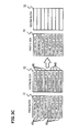
- FIGS. 3A to 3C A specific example of the processes described above is explained with reference to FIGS. 3A to 3C .
- FIGS. 3A to 3C two blocks 31 and 32 in the flash memory 12 are shown.
- eight cells 40 are prepared so as to be able to write data therein.
- three pieces of data for example, first initial data, second initial data, and third initial data are assumed to be a set of data.
- Three pieces of update data that is, first update data, second update data, and third update data are also a set of data.
- data is written sequentially from the top cell 40 in each of the blocks 31 and 32.
- the number of blocks and the number of cells 40 in one block are not limited to those shown in FIGS. 3A to 3C .
- a set of initial data, and respective ones of first update data, second update data, and third update data as the learning values are stored. This indicates that the learning values are updated once from the first to third initial data, respectively. In this case, because there are two free cells 40 in the first block 31, the next update data will be written in the first block 31.
- data is written in all the cells 40 of the first block 31, and data is written in some of the cells 40 of the second block 32.
- the first block 31 three pieces of third update data are stored. This is because while first two learning values have been updated once from the initial data, only the third learning value has been updated three times from the initial data.
- the data search unit 21 checks if there is a set of learning values in the first block 31. In this case, there is a set of learning values including the first to third update data. Therefore, the update data of the learning values, for example, the first update data and the second update data are then written sequentially in the cells 40 of the second block 32.
- the first update data of the first learning value is stored in the first cell while indeterminate data is stored in other cells 40.
- the indeterminate data means data corrupted due to the power on/off operation or data for which a normal end of data write cannot be confirmed.
- indeterminate data is written in a free cell 40 in the second block 32.
- the indeterminate data is written until there is no free cell 40 in the second block 32.
- the data search unit 21 checks if there is a set of learning values in the block 32.
- the data erasure unit 22 erases all pieces of data in the second block 32. Learning values are then written anew in the second block 32 after data erasure.
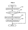
- the data search unit 21 searches for latest data in a currently-used block of the flash memory 12.
- the data search unit 21 checks if there is missing data in a set of learning values. When there is no missing data, the data search unit 21 ends the process. The learning values are then updated in the flash memory 12 according to the flowchart in FIG. 2 .
- Step S203 the data search unit 21 searches the block 31 or 32 one block before for missing data.
- Step S204 the data write unit 23 writes the missing data in a free cell 40 in the block 31 or 32 currently used.
- the third update data is extracted from the previous first block 31 and written in the third cell 40 of the second block 32. Accordingly, a set of learning values becomes prepared completely.
- the data initializing process can be performed also, for example, when a set of learning values is not prepared completely although there is a free cell 40 in the block 31 or 32, as well as at the timing when the power source 2 is turned on.
- a set of learning values stored in the flash memory 12 is expanded in the RAM 11, and the CPU 10 creates a command value for the control target device 5.
- the command value is output to the control target device 5 via the I/F circuit 13.
- a control result of the control target device 5 is fed back to the electronic control device 1 for a vehicle as a detection result from the external device 6 such as a sensor.
- the CPU 10 calculates a new learning value of the control parameter based on the fed back information as needed.
- the calculated new learning value is stored in the flash memory 12 by the data write unit 23 in association with the ID data, which characterizes the type of the learning value.
- the electronic control device 1 can refer to a normal set of learning values in the other block 31 or 32. Therefore, even if a part of data becomes defective, the control target device 5 can be controlled reliably.
- the electronic control device 1 can be configured to output a write request at a timing other than a power-on timing.
Landscapes
- Engineering & Computer Science (AREA)
- Theoretical Computer Science (AREA)
- Physics & Mathematics (AREA)
- General Engineering & Computer Science (AREA)
- General Physics & Mathematics (AREA)
- Techniques For Improving Reliability Of Storages (AREA)
Abstract
Description
- The present invention relates to an electronic control device for a vehicle.
- An electronic control device mounted on a vehicle can learn and update control parameters to be used for engine control. By learning the control parameters, cleaning of exhaust gas and improvement in fuel economy can be achieved. In such an electronic control device, a flash memory is used for a device that stores therein the latest learning values of the parameters to realize cost reduction. In a conventional electronic control device, learning values of a plurality of parameters are temporarily stored in a first memory area of the flash memory and, when an update condition of the learning values is satisfied, the learning values are written in a second memory area of the same flash memory, thereby decreasing the number of times of data erasure for each block of the flash memory (see, for example, Patent Document 1). In the flash memory, data erasure is performed for units of blocks each being an aggregate of a plurality of cells to which data is written. Therefore, by decreasing the number of times of data erasure for each block of the flash memory, the service life of the flash memory is prolonged.
- As a timing to write a new learning value in the flash memory, there is known a timing of a self-shutdown process after a power switch of the vehicle is turned off. However, if a driver turns on the power switch again during the self-shutdown, a writing process of the learning value is forcibly terminated in the middle of writing data to the flash memory, and the learning value data may be recorded in the flash memory in a corrupted state. Therefore, in the conventional electronic control device, when the power switch is turned on again during self-shutdown, the data writing process is not forcibly terminated and a regular process is performed after the writing process ends (see, for example, Patent Document 2).
-
- Patent Document 1: Japanese Patent Application Laid-open Publication No.
2007-179460 - Patent Document 2: Japanese Patent Application Laid-open Publication No.
2008-140373 - In order to reduce the cost of the electronic control device, elimination of a self-shut relay to be used in the self-shutdown process has been examined. However, if the self-shut relay is eliminated, supply of power to the electronic control device is immediately stopped at the time of power off and thus the learning values cannot be written in the flash memory.
- Furthermore, if a power source is turned off during the writing process of a learning value, the learning value may be recorded in the flash memory in a corrupted state. If a power on/off operation is further repeated in this case, corrupted learning values are continuously stored in the flash memory. If all the learning values in the block of the flash memory are corrupted, there is no normal learning value in the block and thus it is difficult to control an engine.
- The present invention has been achieved in view of the above problems, and an object of the present invention is to provide an electronic control device that can obtain learning values of control parameters accurately even if a power on/off operation is repeated.
- The present invention is to provide an electronic control device for a vehicle, the device comprising a flash memory that can store therein respective learning values of a plurality of control parameters and configured to execute predetermined control using the learning values upon reception of supply of power and to be able to store therein the learning values corresponding to the control parameters, respectively, as a set of learning data by adding the learning values newly calculated while power is supplied in a predetermined block of the flash memory, wherein when there is no residual storage capacity to be used space in the predetermined block at a start of the supply of power and the set of learning data is not prepared completely in the predetermined block, data in the predetermined block is erased.
- The present invention also provides the electronic control device for a vehicle according to claim 1, wherein when there is not the set of learning data in the predetermined block at a start of the supply of power, missing one of the learning values in the set of learning data is obtained from another block other than the predetermined block, and the missing learning value is written in the predetermined block.
- According to the present invention, when a set of learning data cannot be obtained in a state where there is no residual storage capacity to be used in a currently-used block of a flash memory, data in the block is erased. Accordingly, it can be prevented that the block is filled with indeterminate data, thereby enabling to reliably perform updating of the leaning values and control using the learning values.
-
- [
FIG. 1] FIG. 1 is a block diagram showing an electronic control device for a vehicle according to an embodiment of the present invention. - [
FIG. 2] FIG. 2 is a flowchart for explaining an updating process of a learning value performed in the electronic control device for a vehicle according to the present embodiment. - [
FIG. 3A] FIG. 3A is an explanatory diagram of an example of data management in a flash memory of the electronic control device for a vehicle according to the present embodiment. - [
FIG. 3B] FIG. 3B is an explanatory diagram of an example of data management in a flash memory of the electronic control device for a vehicle according to the present embodiment. - [
FIG. 3C] FIG. 3C is an explanatory diagram of an example of data management in a flash memory of the electronic control device for a vehicle according to the present embodiment. - [
FIG. 4] FIG. 4 is a flowchart for explaining an initializing process of a learning value performed in the electronic control device for a vehicle according to the present embodiment. - Embodiments of the present invention are explained below in detail.
- As shown in a block diagram of
FIG. 1 , an electronic control device 1 for a vehicle is configured to receive supply of power from apower source 2 via a power supply circuit 3 and to control acontrol target device 5. Specifically, the electronic control device 1 for a vehicle is configured to include a CPU (Central Processing Unit) 10, a RAM (Random Access Memory) 11, aflash memory 12 being a non-volatile storage device, an I/F (interface)circuit 13 connected to thecontrol target device 5, and an I/O (input/output)device 14 connected to anexternal device 6 such as a sensor or an actuator. Thepower source 2 can be a battery or a power generator. Aswitch 7 is provided between thepower source 2 and the power supply circuit 3, and on/off of theswitch 7 is changed according to a command from theCPU 10. - The
CPU 10 can be divided into adata search unit 21 that searches for learning values of control parameters stored in theflash memory 12, adata erasure unit 22 that erases data in a predetermined block of theflash memory 12, and adata write unit 23 that writes learning values in theflash memory 12 and writes initial values of the control parameters therein, which are characteristic functions of the present embodiment. An example of the control parameters is a fully closed value of a throttle valve of an engine. The learning values of the control parameters include, for example, a fully closed value after deterioration with age and a shift amount at a time when the fully closed value of the throttle valve has shifted due to deterioration with age. The type and number of the control parameters and data formats of the learning values are not limited thereto. - Processes performed by the electronic control device 1 for a vehicle are explained next with reference to a flowchart of
FIG. 2 . - First, at Step S101, the data write
unit 23 of theCPU 10 checks if there is a write request of a learning value. The write request is output, for example, at a timing when power supply to the electronic control device 1 for a vehicle is started, that is, when theswitch 7 is turned on. When there is no write request (NO at Step S101), the process at this time ends. - On the other hand, when there is a write request (YES at Step S101), the process proceeds to Step S102 where the
data write unit 23 accesses theflash memory 12 to check if there is a residual storage capacity to be used in a currently-used block of theflash memory 12. When there is a residual storage capacity to be used, the process proceeds to Step S103 (YES at Step S102) where the data writeunit 23 sequentially writes new learning values in a free cell in the current block of theflash memory 12. Subsequently, the process at this time ends. - On the other hand, when there is no residual storage capacity to be used in the currently-used block of the
flash memory 12 at Step S102, the process proceeds to Step S104. At Step S104, thedata search unit 21 checks if there is a set of learning values (a set of learning data) in the currently-used block. As for the set of learning values, for example, when the number of control parameters required for the control of thecontrol target device 5 is three, three learning values corresponding to the control parameters are designated as the set of learning values. If data of at least one of the three learning values is corrupted, thedata search unit 21 determines that the set of learning values is not prepared completely. - The learning values are sequentially stored in the cells of the
flash memory 12 with the learning value data itself being associated with ID (identification) data that specifies the types of the learning values. In order to increase reliability of data, the learning value data itself is stored in theflash memory 12 in such a manner that a plurality of pieces of same data, for example, three pieces of same data are stored therein. In this case, as the corrupted learning value data, such a case is assumed that the ID data is different from expected data or that three data values do not completely agree. Examples of a cause of the corrupted learning value data are a case where thepower source 2 is turned off during write of the learning values and a case where the on/off operation of thepower source 2 is repeated. - When a set of learning data is not prepared completely, the
data search unit 21 judges that an error has occurred in a writing process of the learning values to the cells of theflash memory 12, thereby causing corrupted data. The process then proceeds to Step S105 where thedata erasure unit 22 erases all the pieces of data in the currently-used block of theflash memory 12. Next, at Step S106, the learning values are written in the next block and the process ends. On the other hand, when a set of learning data is prepared completely in the currently-used block of theflash memory 12 at Step S104, the process at Step S106 is performed and then the process ends. - The next block means a block to which write of data can be performed next to a block having no more residual storage capacity to be used. For example, a block from which data has been erased at Step S105 and a block in which the learning values are written at Step S106 can be the same.
- A specific example of the processes described above is explained with reference to
FIGS. 3A to 3C . InFIGS. 3A to 3C , twoblocks flash memory 12 are shown. In each of theblocks cells 40 are prepared so as to be able to write data therein. Regarding the learning values, three pieces of data, for example, first initial data, second initial data, and third initial data are assumed to be a set of data. Three pieces of update data, that is, first update data, second update data, and third update data are also a set of data. Further, it is assumed that data is written sequentially from thetop cell 40 in each of theblocks cells 40 in one block are not limited to those shown inFIGS. 3A to 3C . - In
FIG. 3A , in thefirst block 31 of theflash memory 12, a set of initial data, and respective ones of first update data, second update data, and third update data as the learning values are stored. This indicates that the learning values are updated once from the first to third initial data, respectively. In this case, because there are twofree cells 40 in thefirst block 31, the next update data will be written in thefirst block 31. - In
FIG. 3B , data is written in all thecells 40 of thefirst block 31, and data is written in some of thecells 40 of thesecond block 32. In thefirst block 31, three pieces of third update data are stored. This is because while first two learning values have been updated once from the initial data, only the third learning value has been updated three times from the initial data. After data has been written in eachcell 40 of thefirst block 31, there is no residual storage capacity to be used in the block. Therefore, thedata search unit 21 checks if there is a set of learning values in thefirst block 31. In this case, there is a set of learning values including the first to third update data. Therefore, the update data of the learning values, for example, the first update data and the second update data are then written sequentially in thecells 40 of thesecond block 32. - In the
second block 32 shown inFIG. 3C , the first update data of the first learning value is stored in the first cell while indeterminate data is stored inother cells 40. The indeterminate data means data corrupted due to the power on/off operation or data for which a normal end of data write cannot be confirmed. - When on/off of the
power source 2 is repeated at a timing of writing the next update data after the first update data is written in thefirst cell 40 of thesecond block 32, indeterminate data is written in afree cell 40 in thesecond block 32. The indeterminate data is written until there is nofree cell 40 in thesecond block 32. After data has been written in all thecells 40 in thesecond block 32, thedata search unit 21 checks if there is a set of learning values in theblock 32. - In this case, because there is only one first update data in the
second block 32 and a set of learning values is not prepared completely, thedata erasure unit 22 erases all pieces of data in thesecond block 32. Learning values are then written anew in thesecond block 32 after data erasure. - There are cases where a set of learning values is not in the
blocks power source 2 is turned on. In these cases, a data initializing process is performed, so that a set of learning values can be obtained in one of theblocks FIG. 4 . - First, at Step S201, the
data search unit 21 searches for latest data in a currently-used block of theflash memory 12. At Step S202, thedata search unit 21 checks if there is missing data in a set of learning values. When there is no missing data, thedata search unit 21 ends the process. The learning values are then updated in theflash memory 12 according to the flowchart inFIG. 2 . - On the other hand, when a set of learning values is not prepared completely in the
block data search unit 21 searches theblock unit 23 writes the missing data in afree cell 40 in theblock - For example, in the example shown in
FIG. 3B , there are the first update data and the second update data in thesecond block 32 currently used. However, because there is no third update data, a set of learning values is not prepared completely. Therefore, the third update data is extracted from the previousfirst block 31 and written in thethird cell 40 of thesecond block 32. Accordingly, a set of learning values becomes prepared completely. The data initializing process can be performed also, for example, when a set of learning values is not prepared completely although there is afree cell 40 in theblock power source 2 is turned on. - When the
control target device 5 is to be controlled, a set of learning values stored in theflash memory 12 is expanded in theRAM 11, and theCPU 10 creates a command value for thecontrol target device 5. The command value is output to thecontrol target device 5 via the I/F circuit 13. A control result of thecontrol target device 5 is fed back to the electronic control device 1 for a vehicle as a detection result from theexternal device 6 such as a sensor. TheCPU 10 calculates a new learning value of the control parameter based on the fed back information as needed. The calculated new learning value is stored in theflash memory 12 by the data writeunit 23 in association with the ID data, which characterizes the type of the learning value. - As described above, in the present embodiment, when there is no residual storage capacity to be used, in the currently-used
block flash memory 12 and a set of learning values cannot be obtained, data in theblock cells 40 in theblock block other block control target device 5 can be controlled reliably. - When there is a residual storage capacity to be used in the
block previous block control target device 5 can be reliably controlled. - The present invention is not limited to the above embodiment and can be variously modified without departing from the spirit of the invention. For example, the electronic control device 1 can be configured to output a write request at a timing other than a power-on timing.
-
- 1
- electronic control device
- 2
- power source
- 5
- control target device
- 10
- CPU
- 12
- flash memory
- 21
- data search unit
- 22
- data erasure unit
- 23
- data write unit
- 31
- first block
- 32
- second block
Claims (2)
- An electronic control device for a vehicle, the device comprising a flash memory that can store therein respective learning values of a plurality of control parameters and configured to execute predetermined control using the learning values upon reception of supply of power and to be able to store therein the learning values corresponding to the control parameters, respectively, as a set of learning data by adding the learning values newly calculated while power is supplied in a predetermined block of the flash memory, wherein
when there is no residual storage capacity to be used in the predetermined block at a start of the supply of power and the set of learning data is not prepared completely in the predetermined block, data in the predetermined block is erased. - The electronic control device for a vehicle according to claim 1, wherein when there is not the set of learning data in the predetermined block at a start of the supply of power, missing one of the learning values in the set of learning data is obtained from another block other than the predetermined block, and the missing learning value is written in the predetermined block.
Applications Claiming Priority (2)
| Application Number | Priority Date | Filing Date | Title |
|---|---|---|---|
| JP2012240244A JP5930940B2 (en) | 2012-10-31 | 2012-10-31 | Electronic control device for vehicle |
| PCT/JP2013/078301 WO2014069253A1 (en) | 2012-10-31 | 2013-10-18 | Electronic control device for vehicle |
Publications (3)
| Publication Number | Publication Date |
|---|---|
| EP2916232A1 true EP2916232A1 (en) | 2015-09-09 |
| EP2916232A4 EP2916232A4 (en) | 2016-12-07 |
| EP2916232B1 EP2916232B1 (en) | 2017-12-13 |
Family
ID=50627166
Family Applications (1)
| Application Number | Title | Priority Date | Filing Date |
|---|---|---|---|
| EP13852259.4A Active EP2916232B1 (en) | 2012-10-31 | 2013-10-18 | Electronic control device for vehicle |
Country Status (4)
| Country | Link |
|---|---|
| EP (1) | EP2916232B1 (en) |
| JP (1) | JP5930940B2 (en) |
| CN (1) | CN104737139B (en) |
| WO (1) | WO2014069253A1 (en) |
Families Citing this family (1)
| Publication number | Priority date | Publication date | Assignee | Title |
|---|---|---|---|---|
| KR102552081B1 (en) * | 2018-08-06 | 2023-07-06 | 현대자동차주식회사 | Continuously variable valve duration apparatus and controlling method thereof |
Family Cites Families (6)
| Publication number | Priority date | Publication date | Assignee | Title |
|---|---|---|---|---|
| JP3969494B2 (en) * | 2004-08-31 | 2007-09-05 | 三菱電機株式会社 | In-vehicle electronic control unit |
| JP2006163933A (en) * | 2004-12-08 | 2006-06-22 | Hitachi Ltd | Control data storage device |
| JP2007179460A (en) * | 2005-12-28 | 2007-07-12 | Denso Corp | Electronic control unit |
| JP4937066B2 (en) * | 2006-11-02 | 2012-05-23 | 日立オートモティブシステムズ株式会社 | Electronic control device |
| JP5241408B2 (en) * | 2008-09-26 | 2013-07-17 | ダイハツ工業株式会社 | In-vehicle memory controller |
| JP4647010B2 (en) * | 2009-01-28 | 2011-03-09 | 三菱電機株式会社 | Electronic control unit |
-
2012
- 2012-10-31 JP JP2012240244A patent/JP5930940B2/en not_active Expired - Fee Related
-
2013
- 2013-10-18 EP EP13852259.4A patent/EP2916232B1/en active Active
- 2013-10-18 WO PCT/JP2013/078301 patent/WO2014069253A1/en not_active Ceased
- 2013-10-18 CN CN201380052585.5A patent/CN104737139B/en active Active
Also Published As
| Publication number | Publication date |
|---|---|
| EP2916232B1 (en) | 2017-12-13 |
| JP5930940B2 (en) | 2016-06-08 |
| WO2014069253A1 (en) | 2014-05-08 |
| CN104737139A (en) | 2015-06-24 |
| CN104737139B (en) | 2018-04-06 |
| JP2014089649A (en) | 2014-05-15 |
| EP2916232A4 (en) | 2016-12-07 |
Similar Documents
| Publication | Publication Date | Title |
|---|---|---|
| US10061512B2 (en) | Data storage device and data writing method thereof | |
| US20190287626A1 (en) | Data overwriting device and data overwriting method | |
| US8205070B2 (en) | Device bootup from a NAND-type non-volatile memory | |
| TWI436369B (en) | Methods for measuring usable lifespan and replacing an in-system programming code of a memory device, and data storage system using the same | |
| US20090187305A1 (en) | Method of detecting manipulation of a programmable memory device of a digital controller | |
| US20130046918A1 (en) | Method writing meta data with reduced frequency | |
| CN103186471B (en) | The management method of bad block and system in storage device | |
| US7774382B2 (en) | Method and apparatus for configuring a control device, and corresponding control device | |
| US9195582B2 (en) | Data storing method and apparatus applied to flash memory storage device | |
| KR100823169B1 (en) | Flash memory system with improved operating characteristics and access method thereof | |
| US9786373B2 (en) | EEPROM backup method and device | |
| EP2916232B1 (en) | Electronic control device for vehicle | |
| JP6009290B2 (en) | Electronic control device for vehicle | |
| JP5660521B2 (en) | Nonvolatile semiconductor memory device and memory management method | |
| JP4647010B2 (en) | Electronic control unit | |
| CN109308171B (en) | Data storage method and system for prolonging service life of nonvolatile memory | |
| CN106250193A (en) | A kind of system start method based on nand memory and system | |
| US9773562B2 (en) | Storage apparatus, flash memory control apparatus, and program | |
| US20120026795A1 (en) | Electronic Apparatus and Data Reading Method | |
| US11231871B2 (en) | Electronic control device with non-volatile memory | |
| US10452309B2 (en) | Method and device operating a memory device | |
| US20060123205A1 (en) | Control data storage apparatus and process | |
| CN118276753A (en) | Data storage method, device and storage medium | |
| US10957398B2 (en) | Electronic device with memory erased by page | |
| CN120406822A (en) | Flash self-check method, device, equipment, storage medium and program product |
Legal Events
| Date | Code | Title | Description |
|---|---|---|---|
| PUAI | Public reference made under article 153(3) epc to a published international application that has entered the european phase |
Free format text: ORIGINAL CODE: 0009012 |
|
| 17P | Request for examination filed |
Effective date: 20150410 |
|
| AK | Designated contracting states |
Kind code of ref document: A1 Designated state(s): AL AT BE BG CH CY CZ DE DK EE ES FI FR GB GR HR HU IE IS IT LI LT LU LV MC MK MT NL NO PL PT RO RS SE SI SK SM TR |
|
| AX | Request for extension of the european patent |
Extension state: BA ME |
|
| DAX | Request for extension of the european patent (deleted) | ||
| RA4 | Supplementary search report drawn up and despatched (corrected) |
Effective date: 20161108 |
|
| RIC1 | Information provided on ipc code assigned before grant |
Ipc: G06F 12/16 20060101AFI20161102BHEP Ipc: B60K 6/00 20060101ALI20161102BHEP Ipc: F16F 15/04 20060101ALI20161102BHEP Ipc: B60R 16/02 20060101ALI20161102BHEP Ipc: G06F 12/06 20060101ALI20161102BHEP |
|
| GRAP | Despatch of communication of intention to grant a patent |
Free format text: ORIGINAL CODE: EPIDOSNIGR1 |
|
| STAA | Information on the status of an ep patent application or granted ep patent |
Free format text: STATUS: GRANT OF PATENT IS INTENDED |
|
| RIC1 | Information provided on ipc code assigned before grant |
Ipc: G06F 12/16 20060101AFI20170316BHEP Ipc: B60R 16/02 20060101ALI20170316BHEP Ipc: B60K 6/00 20071001ALI20170316BHEP Ipc: F16F 15/04 20060101ALI20170316BHEP Ipc: G06F 12/06 20060101ALI20170316BHEP |
|
| INTG | Intention to grant announced |
Effective date: 20170412 |
|
| GRAS | Grant fee paid |
Free format text: ORIGINAL CODE: EPIDOSNIGR3 |
|
| GRAJ | Information related to disapproval of communication of intention to grant by the applicant or resumption of examination proceedings by the epo deleted |
Free format text: ORIGINAL CODE: EPIDOSDIGR1 |
|
| GRAL | Information related to payment of fee for publishing/printing deleted |
Free format text: ORIGINAL CODE: EPIDOSDIGR3 |
|
| STAA | Information on the status of an ep patent application or granted ep patent |
Free format text: STATUS: REQUEST FOR EXAMINATION WAS MADE |
|
| INTC | Intention to grant announced (deleted) | ||
| GRAR | Information related to intention to grant a patent recorded |
Free format text: ORIGINAL CODE: EPIDOSNIGR71 |
|
| STAA | Information on the status of an ep patent application or granted ep patent |
Free format text: STATUS: GRANT OF PATENT IS INTENDED |
|
| GRAA | (expected) grant |
Free format text: ORIGINAL CODE: 0009210 |
|
| STAA | Information on the status of an ep patent application or granted ep patent |
Free format text: STATUS: THE PATENT HAS BEEN GRANTED |
|
| INTG | Intention to grant announced |
Effective date: 20171106 |
|
| REG | Reference to a national code |
Ref country code: GB Ref legal event code: FG4D |
|
| REG | Reference to a national code |
Ref country code: AT Ref legal event code: REF Ref document number: 955020 Country of ref document: AT Kind code of ref document: T Effective date: 20171215 Ref country code: CH Ref legal event code: EP |
|
| REG | Reference to a national code |
Ref country code: IE Ref legal event code: FG4D |
|
| REG | Reference to a national code |
Ref country code: DE Ref legal event code: R096 Ref document number: 602013030919 Country of ref document: DE |
|
| REG | Reference to a national code |
Ref country code: NL Ref legal event code: MP Effective date: 20171213 |
|
| PG25 | Lapsed in a contracting state [announced via postgrant information from national office to epo] |
Ref country code: FI Free format text: LAPSE BECAUSE OF FAILURE TO SUBMIT A TRANSLATION OF THE DESCRIPTION OR TO PAY THE FEE WITHIN THE PRESCRIBED TIME-LIMIT Effective date: 20171213 Ref country code: SE Free format text: LAPSE BECAUSE OF FAILURE TO SUBMIT A TRANSLATION OF THE DESCRIPTION OR TO PAY THE FEE WITHIN THE PRESCRIBED TIME-LIMIT Effective date: 20171213 Ref country code: NO Free format text: LAPSE BECAUSE OF FAILURE TO SUBMIT A TRANSLATION OF THE DESCRIPTION OR TO PAY THE FEE WITHIN THE PRESCRIBED TIME-LIMIT Effective date: 20180313 |
|
| REG | Reference to a national code |
Ref country code: AT Ref legal event code: MK05 Ref document number: 955020 Country of ref document: AT Kind code of ref document: T Effective date: 20171213 |
|
| PG25 | Lapsed in a contracting state [announced via postgrant information from national office to epo] |
Ref country code: RS Free format text: LAPSE BECAUSE OF FAILURE TO SUBMIT A TRANSLATION OF THE DESCRIPTION OR TO PAY THE FEE WITHIN THE PRESCRIBED TIME-LIMIT Effective date: 20171213 Ref country code: LV Free format text: LAPSE BECAUSE OF FAILURE TO SUBMIT A TRANSLATION OF THE DESCRIPTION OR TO PAY THE FEE WITHIN THE PRESCRIBED TIME-LIMIT Effective date: 20171213 Ref country code: HR Free format text: LAPSE BECAUSE OF FAILURE TO SUBMIT A TRANSLATION OF THE DESCRIPTION OR TO PAY THE FEE WITHIN THE PRESCRIBED TIME-LIMIT Effective date: 20171213 Ref country code: BG Free format text: LAPSE BECAUSE OF FAILURE TO SUBMIT A TRANSLATION OF THE DESCRIPTION OR TO PAY THE FEE WITHIN THE PRESCRIBED TIME-LIMIT Effective date: 20180313 Ref country code: GR Free format text: LAPSE BECAUSE OF FAILURE TO SUBMIT A TRANSLATION OF THE DESCRIPTION OR TO PAY THE FEE WITHIN THE PRESCRIBED TIME-LIMIT Effective date: 20180314 |
|
| PG25 | Lapsed in a contracting state [announced via postgrant information from national office to epo] |
Ref country code: NL Free format text: LAPSE BECAUSE OF FAILURE TO SUBMIT A TRANSLATION OF THE DESCRIPTION OR TO PAY THE FEE WITHIN THE PRESCRIBED TIME-LIMIT Effective date: 20171213 |
|
| PG25 | Lapsed in a contracting state [announced via postgrant information from national office to epo] |
Ref country code: ES Free format text: LAPSE BECAUSE OF FAILURE TO SUBMIT A TRANSLATION OF THE DESCRIPTION OR TO PAY THE FEE WITHIN THE PRESCRIBED TIME-LIMIT Effective date: 20171213 Ref country code: CZ Free format text: LAPSE BECAUSE OF FAILURE TO SUBMIT A TRANSLATION OF THE DESCRIPTION OR TO PAY THE FEE WITHIN THE PRESCRIBED TIME-LIMIT Effective date: 20171213 Ref country code: SK Free format text: LAPSE BECAUSE OF FAILURE TO SUBMIT A TRANSLATION OF THE DESCRIPTION OR TO PAY THE FEE WITHIN THE PRESCRIBED TIME-LIMIT Effective date: 20171213 Ref country code: EE Free format text: LAPSE BECAUSE OF FAILURE TO SUBMIT A TRANSLATION OF THE DESCRIPTION OR TO PAY THE FEE WITHIN THE PRESCRIBED TIME-LIMIT Effective date: 20171213 Ref country code: CY Free format text: LAPSE BECAUSE OF FAILURE TO SUBMIT A TRANSLATION OF THE DESCRIPTION OR TO PAY THE FEE WITHIN THE PRESCRIBED TIME-LIMIT Effective date: 20171213 |
|
| PG25 | Lapsed in a contracting state [announced via postgrant information from national office to epo] |
Ref country code: RO Free format text: LAPSE BECAUSE OF FAILURE TO SUBMIT A TRANSLATION OF THE DESCRIPTION OR TO PAY THE FEE WITHIN THE PRESCRIBED TIME-LIMIT Effective date: 20171213 Ref country code: IS Free format text: LAPSE BECAUSE OF FAILURE TO SUBMIT A TRANSLATION OF THE DESCRIPTION OR TO PAY THE FEE WITHIN THE PRESCRIBED TIME-LIMIT Effective date: 20180413 Ref country code: SM Free format text: LAPSE BECAUSE OF FAILURE TO SUBMIT A TRANSLATION OF THE DESCRIPTION OR TO PAY THE FEE WITHIN THE PRESCRIBED TIME-LIMIT Effective date: 20171213 Ref country code: PL Free format text: LAPSE BECAUSE OF FAILURE TO SUBMIT A TRANSLATION OF THE DESCRIPTION OR TO PAY THE FEE WITHIN THE PRESCRIBED TIME-LIMIT Effective date: 20171213 Ref country code: AT Free format text: LAPSE BECAUSE OF FAILURE TO SUBMIT A TRANSLATION OF THE DESCRIPTION OR TO PAY THE FEE WITHIN THE PRESCRIBED TIME-LIMIT Effective date: 20171213 |
|
| REG | Reference to a national code |
Ref country code: FR Ref legal event code: PLFP Year of fee payment: 6 |
|
| REG | Reference to a national code |
Ref country code: DE Ref legal event code: R097 Ref document number: 602013030919 Country of ref document: DE |
|
| PLBE | No opposition filed within time limit |
Free format text: ORIGINAL CODE: 0009261 |
|
| STAA | Information on the status of an ep patent application or granted ep patent |
Free format text: STATUS: NO OPPOSITION FILED WITHIN TIME LIMIT |
|
| 26N | No opposition filed |
Effective date: 20180914 |
|
| PG25 | Lapsed in a contracting state [announced via postgrant information from national office to epo] |
Ref country code: DK Free format text: LAPSE BECAUSE OF FAILURE TO SUBMIT A TRANSLATION OF THE DESCRIPTION OR TO PAY THE FEE WITHIN THE PRESCRIBED TIME-LIMIT Effective date: 20171213 |
|
| PG25 | Lapsed in a contracting state [announced via postgrant information from national office to epo] |
Ref country code: SI Free format text: LAPSE BECAUSE OF FAILURE TO SUBMIT A TRANSLATION OF THE DESCRIPTION OR TO PAY THE FEE WITHIN THE PRESCRIBED TIME-LIMIT Effective date: 20171213 |
|
| REG | Reference to a national code |
Ref country code: CH Ref legal event code: PL |
|
| REG | Reference to a national code |
Ref country code: BE Ref legal event code: MM Effective date: 20181031 |
|
| PG25 | Lapsed in a contracting state [announced via postgrant information from national office to epo] |
Ref country code: MC Free format text: LAPSE BECAUSE OF FAILURE TO SUBMIT A TRANSLATION OF THE DESCRIPTION OR TO PAY THE FEE WITHIN THE PRESCRIBED TIME-LIMIT Effective date: 20171213 Ref country code: LU Free format text: LAPSE BECAUSE OF NON-PAYMENT OF DUE FEES Effective date: 20181018 |
|
| REG | Reference to a national code |
Ref country code: IE Ref legal event code: MM4A |
|
| PG25 | Lapsed in a contracting state [announced via postgrant information from national office to epo] |
Ref country code: LI Free format text: LAPSE BECAUSE OF NON-PAYMENT OF DUE FEES Effective date: 20181031 Ref country code: CH Free format text: LAPSE BECAUSE OF NON-PAYMENT OF DUE FEES Effective date: 20181031 Ref country code: BE Free format text: LAPSE BECAUSE OF NON-PAYMENT OF DUE FEES Effective date: 20181031 |
|
| PG25 | Lapsed in a contracting state [announced via postgrant information from national office to epo] |
Ref country code: IE Free format text: LAPSE BECAUSE OF NON-PAYMENT OF DUE FEES Effective date: 20181018 |
|
| PG25 | Lapsed in a contracting state [announced via postgrant information from national office to epo] |
Ref country code: MT Free format text: LAPSE BECAUSE OF NON-PAYMENT OF DUE FEES Effective date: 20181018 |
|
| PG25 | Lapsed in a contracting state [announced via postgrant information from national office to epo] |
Ref country code: TR Free format text: LAPSE BECAUSE OF FAILURE TO SUBMIT A TRANSLATION OF THE DESCRIPTION OR TO PAY THE FEE WITHIN THE PRESCRIBED TIME-LIMIT Effective date: 20171213 |
|
| PG25 | Lapsed in a contracting state [announced via postgrant information from national office to epo] |
Ref country code: PT Free format text: LAPSE BECAUSE OF FAILURE TO SUBMIT A TRANSLATION OF THE DESCRIPTION OR TO PAY THE FEE WITHIN THE PRESCRIBED TIME-LIMIT Effective date: 20171213 |
|
| PG25 | Lapsed in a contracting state [announced via postgrant information from national office to epo] |
Ref country code: HU Free format text: LAPSE BECAUSE OF FAILURE TO SUBMIT A TRANSLATION OF THE DESCRIPTION OR TO PAY THE FEE WITHIN THE PRESCRIBED TIME-LIMIT; INVALID AB INITIO Effective date: 20131018 Ref country code: LT Free format text: LAPSE BECAUSE OF FAILURE TO SUBMIT A TRANSLATION OF THE DESCRIPTION OR TO PAY THE FEE WITHIN THE PRESCRIBED TIME-LIMIT Effective date: 20171213 Ref country code: MK Free format text: LAPSE BECAUSE OF NON-PAYMENT OF DUE FEES Effective date: 20171213 |
|
| PG25 | Lapsed in a contracting state [announced via postgrant information from national office to epo] |
Ref country code: AL Free format text: LAPSE BECAUSE OF FAILURE TO SUBMIT A TRANSLATION OF THE DESCRIPTION OR TO PAY THE FEE WITHIN THE PRESCRIBED TIME-LIMIT Effective date: 20171213 |
|
| REG | Reference to a national code |
Ref country code: GB Ref legal event code: 732E Free format text: REGISTERED BETWEEN 20211210 AND 20211215 |
|
| REG | Reference to a national code |
Ref country code: DE Ref legal event code: R081 Ref document number: 602013030919 Country of ref document: DE Owner name: HITACHI ASTEMO, LTD., HITACHINAKA-SHI, JP Free format text: FORMER OWNER: KEIHIN CORPORATION, TOKYO, JP |
|
| PGFP | Annual fee paid to national office [announced via postgrant information from national office to epo] |
Ref country code: GB Payment date: 20240829 Year of fee payment: 12 |
|
| PGFP | Annual fee paid to national office [announced via postgrant information from national office to epo] |
Ref country code: FR Payment date: 20240909 Year of fee payment: 12 |
|
| PGFP | Annual fee paid to national office [announced via postgrant information from national office to epo] |
Ref country code: IT Payment date: 20240910 Year of fee payment: 12 |
|
| PGFP | Annual fee paid to national office [announced via postgrant information from national office to epo] |
Ref country code: DE Payment date: 20240828 Year of fee payment: 12 |