EP2916203A1 - Touch panel and display apparatus including the same - Google Patents
Touch panel and display apparatus including the same Download PDFInfo
- Publication number
- EP2916203A1 EP2916203A1 EP15156275.8A EP15156275A EP2916203A1 EP 2916203 A1 EP2916203 A1 EP 2916203A1 EP 15156275 A EP15156275 A EP 15156275A EP 2916203 A1 EP2916203 A1 EP 2916203A1
- Authority
- EP
- European Patent Office
- Prior art keywords
- conductive pattern
- peripheral members
- touch panel
- main member
- region
- Prior art date
- Legal status (The legal status is an assumption and is not a legal conclusion. Google has not performed a legal analysis and makes no representation as to the accuracy of the status listed.)
- Withdrawn
Links
Images


Classifications
-
- G—PHYSICS
- G06—COMPUTING OR CALCULATING; COUNTING
- G06F—ELECTRIC DIGITAL DATA PROCESSING
- G06F3/00—Input arrangements for transferring data to be processed into a form capable of being handled by the computer; Output arrangements for transferring data from processing unit to output unit, e.g. interface arrangements
- G06F3/01—Input arrangements or combined input and output arrangements for interaction between user and computer
- G06F3/03—Arrangements for converting the position or the displacement of a member into a coded form
- G06F3/041—Digitisers, e.g. for touch screens or touch pads, characterised by the transducing means
-
- G—PHYSICS
- G06—COMPUTING OR CALCULATING; COUNTING
- G06F—ELECTRIC DIGITAL DATA PROCESSING
- G06F3/00—Input arrangements for transferring data to be processed into a form capable of being handled by the computer; Output arrangements for transferring data from processing unit to output unit, e.g. interface arrangements
- G06F3/01—Input arrangements or combined input and output arrangements for interaction between user and computer
- G06F3/03—Arrangements for converting the position or the displacement of a member into a coded form
- G06F3/041—Digitisers, e.g. for touch screens or touch pads, characterised by the transducing means
- G06F3/044—Digitisers, e.g. for touch screens or touch pads, characterised by the transducing means by capacitive means
- G06F3/0445—Digitisers, e.g. for touch screens or touch pads, characterised by the transducing means by capacitive means using two or more layers of sensing electrodes, e.g. using two layers of electrodes separated by a dielectric layer
-
- G—PHYSICS
- G06—COMPUTING OR CALCULATING; COUNTING
- G06F—ELECTRIC DIGITAL DATA PROCESSING
- G06F3/00—Input arrangements for transferring data to be processed into a form capable of being handled by the computer; Output arrangements for transferring data from processing unit to output unit, e.g. interface arrangements
- G06F3/01—Input arrangements or combined input and output arrangements for interaction between user and computer
- G06F3/03—Arrangements for converting the position or the displacement of a member into a coded form
- G06F3/041—Digitisers, e.g. for touch screens or touch pads, characterised by the transducing means
- G06F3/0412—Digitisers structurally integrated in a display
-
- G—PHYSICS
- G06—COMPUTING OR CALCULATING; COUNTING
- G06F—ELECTRIC DIGITAL DATA PROCESSING
- G06F2203/00—Indexing scheme relating to G06F3/00 - G06F3/048
- G06F2203/041—Indexing scheme relating to G06F3/041 - G06F3/045
- G06F2203/04111—Cross over in capacitive digitiser, i.e. details of structures for connecting electrodes of the sensing pattern where the connections cross each other, e.g. bridge structures comprising an insulating layer, or vias through substrate
Definitions
- the invention relates to a touch panel and a display apparatus including the touch panel.
- Touch panels have recently been used in various fields because they may function as an input device when touched by a user's finger or a pen without using other input units, such as a keyboard.
- display apparatuses have recently been replaced with portable, thin, flat-panel type display apparatuses, in which the technology of applying a touch panel function to the flat-panel type display apparatuses is used.
- a touch panel may include conductive patterns.
- Position control in a touch panel requires higher precision according to demand by users. Consequently, when a user touches the touch panel, it is necessary to sense a fine variation of the touch location on the touch panel.
- the invention sets-out to provide a touch panel and a display apparatus capable of improving precision in touch recognition and user convenience.
- a touch panel includes: a base portion having a thickness that varies according to applied pressure; a first conductive pattern unit disposed on a first surface of the base portion and including first conductive patterns; and a second conductive pattern unit disposed on a second surface of the base portion opposing the first conductive pattern unit and including second conductive patterns that overlap with the first conductive patterns.
- Each of the first conductive patterns may include regions overlapping with the second conductive patterns, and in one of the overlapping regions, an amount of overlapping area between the first conductive pattern and the second conductive pattern decreases the farther away radially the overlapping area is from a center point of the overlapping region.
- a display apparatus includes a touch panel and a display panel, the touch panel including: a base portion having a thickness that varies according to pressure; a first conductive pattern unit disposed on a first surface of the base portion and including first conductive patterns; and a second conductive pattern unit disposed on a second surface of the base portion opposing the first conductive pattern unit and including second conductive patterns that overlap with the first conductive patterns.
- Each of the first conductive patterns may include regions overlapping with the second conductive patterns, and in one of the overlapping regions, an amount of overlapping area between the first conductive pattern and the second conductive pattern may decrease the farther away radially the overlapping area is from a center point of the overlapping region.
- the touch panel may be disposed to face a surface of the display panel, which displays images, or an opposite surface.
- an element or layer When an element or layer is referred to as being “on,” “connected to,” or “coupled to” another element or layer, it may be directly on, connected to, or coupled to the other element or layer or intervening elements or layers may be present. When, however, an element or layer is referred to as being “directly on,” “directly connected to,” or “directly coupled to” another element or layer, there are no intervening elements or layers present.
- X, Y, and Z and "at least one selected from the group consisting of X, Y, and Z” may be construed as X only, Y only, Z only, or any combination of two or more of X, Y, and Z, such as, for instance, XYZ, XYY, YZ, and ZZ.
- XYZ XYY
- YZ YZ
- ZZ ZZ
- first, second, etc. may be used herein to describe various elements, components, regions, layers, and/or sections, these elements, components, regions, layers, and/or sections should not be limited by these terms. These terms are used to distinguish one element, component, region, layer, and/or section from another element, component, region, layer, and/or section. Thus, a first element, component, region, layer, and/or section discussed below could be termed a second element, component, region, layer, and/or section without departing from the teachings of the present disclosure.
- Spatially relative terms such as “beneath,” “below,” “lower,” “above,” “upper,” and the like, may be used herein for descriptive purposes, and, thereby, to describe one element or feature's relationship to another element(s) or feature(s) as illustrated in the drawings.
- Spatially relative terms are intended to encompass different orientations of an apparatus in use, operation, and/or manufacture in addition to the orientation depicted in the drawings. For example, if the apparatus in the drawings is turned over, elements described as “below” or “beneath” other elements or features would then be oriented “above” the other elements or features.
- the exemplary term “below” can encompass both an orientation of above and below.
- the apparatus may be otherwise oriented (e.g., rotated 90 degrees or at other orientations), and, as such, the spatially relative descriptors used herein interpreted accordingly.
- the x-axis, the y-axis and the z-axis are not limited to three axes of the rectangular coordinate system, and may be interpreted in a broader sense.
- the x-axis, the y-axis, and the z-axis may be perpendicular to one another, or may represent different directions that are not perpendicular to one another.
- a specific process order may be performed differently from the described order. For example, two consecutively described processes may be performed substantially at the same time or performed in an order opposite to the described order. Expressions such as "at least one of,” when preceding a list of elements, modify the entire list of elements and do not modify the individual elements of the list.
- a touch panel 100 includes a base portion 101, the first conductive pattern unit 110, and the second conductive pattern unit 120.
- the thickness of the base portion 101, between an upper surface and a lower surface thereof, may be reduced by the application of pressure.
- the base portion 101 may be formed of various materials, for example, silicon or a plastic material.
- the plastic material forming the base portion 101 may include one or more of various organic materials.
- the first conductive pattern unit 110 and the second conductive pattern unit 120 are disposed on different surfaces of the base portion 101, that is, surfaces of the base portion 101 that face away from each other.
- the first conductive pattern unit 110 may be disposed on an upper surface of the base portion 101
- the second conductive pattern unit 120 may be disposed on a lower surface of the base portion 101.
- the first conductive pattern unit 110 includes first conductive patterns 111 through 115. In FIG. 2 , for example, five conductive patterns 111 through 115 are shown, but there is no limitation in the number of the first conductive patterns in the first conductive pattern unit 110.
- the first conductive patterns 111 through 115 are sequentially arranged in a first direction (X-axis direction of FIG. 2 ) and are spaced apart from each other.
- the first conductive pattern 111 includes a main member MU and peripheral members SU.
- the main member MU of the first conductive pattern 111 is arranged at the center of the first conductive pattern 111, and extends lengthwise in a second direction (Y-axis direction in FIG. 2 ) that crosses the first direction (X-axis direction of FIG. 2 ) in which the first conductive patterns 111 and 115 are sequentially arranged and are spaced apart from each other.
- the main member MU may cross so as to be perpendicular to the first direction (X-axis direction of FIG. 2 ).
- the peripheral members SU of the first conductive pattern 111 are disposed on a periphery of the main member MU to protrude from the main member MU. That is, the peripheral members SU of the first conductive pattern 111 are formed between the main member MU of the first conductive pattern 111 and the main member MU of the first conductive pattern 112 adjacent to the first conductive pattern 111. For example, the peripheral members SU of the first conductive pattern 111 may protrude toward the first conductive pattern 112.
- Each of the peripheral members SU of the first conductive pattern 111 extends from a side surface of the main member MU, and has a width that decreases gradually in a direction toward the first conductive pattern 112 adjacent to the first conductive pattern 111.
- the first conductive pattern 111 may include triangularly-shaped peripheral members SU.
- triangularly-shaped spaces are formed between the peripheral members SU.
- the peripheral members SU of the first conductive pattern 112 adjacent to the first conductive pattern 111 are disposed in the triangularly-shaped spaces.
- the peripheral members SU of the first conductive pattern 111 may be formed in a saw-tooth pattern, and the peripheral members SU of the first conductive pattern 112 adjacent to the first conductive pattern 111 may be formed in a similar saw-tooth pattern.
- the peripheral members SU of the first conductive pattern 111 and the peripheral members SU of the first conductive pattern 112 may be alternately disposed.
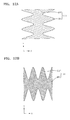
- the peripheral members SU of the first conductive pattern 111 may have curved shapes. That is, the peripheral members SU of the first conductive pattern 111 may extend from the side surface of the main member MU, and may have curved shapes having widths that are gradually reduced toward the first conductive pattern 112 adjacent to the first conductive pattern 111 as shown in FIG. 12A .
- the first conductive pattern 112 is disposed adjacent to the first conductive pattern 111.
- the peripheral members SU of the first conductive pattern 112 are disposed between the peripheral members SU of the first conductive pattern 111 and the first conductive pattern 113 adjacent to the first conductive pattern 112.
- the first conductive patterns 112 through 115 are the same as the first conductive pattern 111, and thus, detailed descriptions thereof are not provided here.
- the second conductive pattern unit 120 includes second conductive patterns 121 through 125. In FIG. 3 , for example, five conductive patterns 121 through 125 are shown, but there is no limitation in the number of second conductive patterns in the second conductive pattern unit 120.
- the second conductive patterns 121 through 125 are sequentially arranged in the second direction (Y-axis direction of FIG. 3 ) and are spaced apart from each other. Also, the second conductive patterns 121 through 125 cross the first conductive patterns 111 through 115 to overlap with the first conductive patterns 111 through 115.
- the second conductive pattern 121 includes a main member MU and peripheral members SU.
- the main member MU of the second conductive pattern 121 is arranged at the center of the second conductive pattern 121 and extends lengthwise in the first direction (X-axis direction in FIG. 3 ) that crosses the second direction (Y-axis direction of FIG. 3 ) in which the second conductive patterns 121 and 125 are sequentially arranged and are spaced apart from each other.
- the main member MU may cross so as to be perpendicular to the second direction (Y-axis direction of FIG. 3 ).
- the peripheral members SU of the second conductive pattern 121 are disposed on a periphery of the main member MU to protrude from the main member MU. That is, the peripheral members SU of the second conductive pattern 121 are formed between the main member MU of the second conductive pattern 121 and the main member MU of the second conductive pattern 122 adjacent to the second conductive pattern 121. For example, the peripheral members SU of the second conductive pattern 121 may protrude toward the second conductive pattern 122.
- the second conductive pattern 121 includes peripheral members SU.
- Each of the peripheral members SU of the second conductive pattern 121 extends from a side surface of the main member MU, and has a width that is reduced gradually in a direction toward the second conductive pattern 122 adjacent to the second conductive pattern 121.
- the second conductive pattern 121 may include triangularly-shaped peripheral members SU.
- triangularly-shaped spaces are formed between the peripheral members SU.
- the peripheral members SU of the second conductive pattern 122 adjacent to the second conductive pattern 121 are disposed in the triangularly-shaped spaces.
- the peripheral members SU of the second conductive pattern 121 may be formed in a saw-tooth pattern, and the peripheral members SU of the second conductive pattern 122 adjacent to the second conductive pattern 121 may also be formed in a similar saw-tooth pattern.
- the peripheral members SU of the second conductive pattern 121 and the peripheral members SU of the second conductive pattern 122 may be alternately disposed.
- the peripheral members SU of the second conductive pattern 121 may have curved shapes. That is, the peripheral members SU of the second conductive pattern 121 may extend from the side surface of the main member MU, and may have curved shapes having widths that are gradually reduced toward the second conductive pattern 122 adjacent to the second conductive pattern 121 as shown in FIG. 12B ..
- the second conductive pattern 122 is disposed adjacent to the second conductive pattern 121.
- the peripheral members SU of the second conductive pattern 122 are disposed between the peripheral members SU of the second conductive pattern 121 and the second conductive pattern 123 adjacent to the second conductive pattern 122.
- the second conductive patterns 122 through 125 are the same as the second conductive pattern 121, and thus, detailed descriptions thereof are not provided here.
- FIG. 4 is a plan view of an overlapping portion between the first conductive pattern unit 110 and the second conductive pattern unit 120 in the touch panel 100 of FIG. 1 .
- the first conductive pattern unit 110 is disposed on the upper surface of the base portion 101, and the second conductive pattern unit 120 is disposed on the lower surface of the base portion 101.
- the first conductive pattern unit 110 and the second conductive pattern unit 120 may partially overlap with each other.
- the first conductive pattern 111 of the first conductive pattern unit 110 overlaps with each of the second conductive patterns 121 through 125 in the second conductive pattern unit 120.
- an overlapping unit OU between the first conductive pattern 111 and the second conductive pattern 121 is shown in order to describe a region in which the first conductive pattern 111 of the first conductive pattern unit 110 and the second conductive pattern 121 of the second conductive pattern unit 120 overlap with each other.
- the area of the overlapping region between the first conductive pattern 111 and the second conductive pattern 121 decreases the farther away it is from a center point C of the overlapping unit OU in the X-axis direction. Also, the area of the overlapping region between the first conductive pattern 111 and the second conductive pattern 121 decreases the farther away it is from the center point C of the overlapping unit OU in the Y-axis direction. Consequently, the area of the overlapping region between the first conductive pattern 111 and the second conductive pattern 121 decreases the farther away it is radially from the center point C of the overlapping unit OU.
- FIGS. 5 and 6 are diagrams illustrating examples of operating the touch panel 100 of FIG. 1 .
- FIG. 7A are graphs showing results of operating the touch panel in FIGS. 5 and 6 .
- a user touches two points A and B from above the base portion 101.
- the touches are on an upper surface of the first conductive pattern 112 of the first conductive pattern unit 110.
- FIG. 6 is a plan view of the touch panel of FIG. 5 .
- a pressure generated by the touch is transferred to the first conductive pattern unit 110 and the base portion 101.
- the base portion 101 is contracted by the pressure, and thus, a thickness of the portion in the base portion 101, on which the user's touch occurs, is reduced.
- a distance between locations, which correspond to the touched point, of the first conductive pattern unit 110 and the second conductive pattern unit 120 is reduced, while the base portion 101 is interposed between the first conductive pattern unit 110 and the second conductive pattern unit 120.
- the elasticity of the base portion 101 is set, such that when pressure corresponding to a touch (touch pressure) is applied thereto, the thickness of the base portion 101 is reduced in a portion where the touch pressure is applied.
- touch pressure refers to an amount of pressure that is generally applied to a touch screen by contact with an external object, such as a finger or stylus.
- an electrostatic capacitance between the first conductive pattern unit 110 and the second conductive pattern unit 120 is changed, and the touch panel 100 recognizes the user's touch by sensing a change in the electric signal, such as the variation in the electrostatic capacitance.
- the user may touch two points A and B in one of the first conductive patterns of the first conductive pattern unit 110, for example, in the first conductive pattern 112.
- the thickness of the base portion 101 rarely changes in locations corresponding to the first conductive patterns 111 and 113 that are adjacent to the first conductive pattern 112. Therefore, the electric signal between the first conductive pattern 111 and the second conductive pattern 121 and the electric signal between the first conductive pattern 113 and the second conductive pattern 121 are not changed.
- a graph of FIG. 7A shows the above result in detail. That is, in the graph of FIG. 7A , an X-axis denotes the first conductive patterns 111, 112, and 113, and a Y-axis denotes a variation amount of electrostatic capacitances (ES) between each of the first conductive patterns 111 through 113 and the second conductive pattern 121.
- ES electrostatic capacitances
- the first conductive pattern 113 adjacent to the first conductive pattern 112 is affected, whereas the first conductive pattern 111 is not.
- the point B corresponds to an edge of the first conductive pattern 112, that is, the peripheral member SU, and is adjacent to the peripheral member SU of the first conductive pattern 113. That is, when the thickness of the base portion 101 corresponding to the point B is changed, a thickness of a region in the base portion 101, which corresponds to the peripheral member SU of the first conductive pattern 113 adjacent to the point B is also changed.
- FIG. 7B shows a result of the above operation. That is, in the graph of FIG. 7B , an X-axis denotes the first conductive patterns 111, 112, and 113, and a Y-axis denotes a variation amount in an electrostatic capacitance (ES) between each of the first conductive patterns 111 through 113, and the second conductive pattern 121.
- ES electrostatic capacitance
- the touch panel 100 of the present embodiment magnitudes and kinds of the electric signals differ from each other when the point A is touched and the point B is touched in the first conductive pattern unit 110.
- the touch panel 100 may recognize the touches on the point A and the point B in the first conductive pattern unit 110 as different kinds of touches, and thus, may recognize the touch input accurately.
- effects on the first conductive pattern 112 adjacent to the first conductive pattern 111 may be different in a case where a region corresponding to the main member MU is touched and in a case where a region corresponding to the peripheral member SU is touched.
- a difference between the thickness of the base portion 101 caused by the pressure generated when touching the touch screen 100 may cause the distance between the first conductive pattern unit 110 and the second conductive pattern unit 120 to vary.
- a difference in the amount of variation of the electrostatic capacitance is generated.
- the distances between the first conductive pattern 112 adjacent to the first conductive pattern 111 and the second conductive pattern 121 are changed a small amount, which cause the variation in the electrostatic capacitance.
- the thickness variation of the base portion 101 may be recognized with high sensitivity as a result of the peripheral members SU of the first conductive pattern 112, which are sequentially arranged between the peripheral members SU of the first conductive pattern 111. Accordingly, the amount of variation in the electrostatic capacitance may be sensed accurately, and precision of the touch recognition may be improved.
- FIG. 8A shows a first conductive pattern 211 included in a first conductive pattern unit
- FIG. 8B shows a second conductive pattern 221 included in a second conductive pattern unit
- FIG. 8C shows an overlapping region between the first conductive pattern 211 and the second conductive pattern 221.
- the first conductive pattern unit may include a plurality of first conductive patterns in addition to the first conductive pattern 211.
- the first conductive pattern 211 includes a main member MU and peripheral members SU.
- the main member MU of the first conductive pattern 211 is arranged at a center of the first conductive pattern 211, and is elongated.
- the peripheral members SU of the first conductive pattern 211 are disposed around the main member MU and protrude from the main member MU.
- Each of the peripheral members SU includes a first region SU1 and a second region SU2.
- the first region SU1 is connected to the main member MU, and the second region SU2 is connected to the first region SU1.
- the second region SU2 is formed to have a width that is less than that of the first region SU1.
- the first region SU1 has a rectangular shape
- the second region SU2 has a rectangular shape that is connected to the first region SU1.
- a side surface of the main member MU has portions that are not connected to the first regions SU1. That is, the side surface of the main member MU includes lateral regions corresponding to spaces between the first regions SU1.
- Second regions SU2 of the peripheral members SU of another first conductive pattern may be arranged to be close to the lateral regions of the main member MU. Accordingly, precision of the touch recognition with respect to the touches on the different locations corresponding to the main member may be improved.
- the first conductive pattern 211 includes the peripheral members SU. Empty spaces are formed between the peripheral members SU. In addition, the peripheral members of another first conductive pattern (not shown) adjacent to the first conductive pattern 211 are disposed in the empty spaces.
- each of the peripheral members SU extends from the side surface of the main member MU, and as described above, the peripheral members SU are arranged to have preset intervals therebetween so as not to cover the entire side surface of the main member MU.
- FIG. 8B shows only a second conductive pattern 221.
- the second conductive pattern unit may include a plurality of second conductive patterns in addition to the second conductive pattern 221, as described above.
- the second conductive pattern 221 includes a main member MU and peripheral members SU.
- the main member MU of the second conductive pattern 221 is arranged at a center of the second conductive pattern 221, and is elongated.
- the main member MU of the second conductive pattern 221 may be elongated in a direction that crosses the main member MU of the first conductive pattern 211 or that is perpendicular to the main member MU of the first conductive pattern 211.
- the peripheral members SU of the second conductive pattern 221 are arranged around the main member MU, and protrude from the main member MU.
- Each of the peripheral members SU includes a first region SU1 and a second region SU2.
- the first region SU1 is connected to the main member MU, and the second region SU2 is connected to the first region SU1.
- the second region SU2 is formed to have a width that is less than that of the first region SU1.
- the first region SU1 has a rectangular shape
- the second region SU2 has a rectangular shape that is connected to the first region SU1.
- a side surface of the main member MU has portions that are not connected to the first regions SU1. That is, the side surface of the main member MU includes lateral regions corresponding to empty spaces between the first regions SU1.
- Second regions SU2 of the peripheral members SU of another first conductive pattern may be arranged to be close to the lateral regions of the main member MU. Accordingly, precision of the touch recognition with respect to the touches on the different locations corresponding to the main member may be improved.
- the second conductive pattern 221 includes the peripheral members SU extending from the side surface of the main member MU. Empty spaces are formed between the peripheral members SU. In addition, the peripheral members of another second conductive pattern (not shown) adjacent to the second conductive pattern 221 are disposed in the empty spaces.
- Each of the peripheral members SU extends from the side surface of the main member MU, and as described above, the peripheral members SU are arranged to have intervals therebetween so as not to cover the entire side surface of the main member MU.
- FIG. 8C shows an overlapping region between the first conductive pattern 211 and the second conductive pattern 221. That is, as described in the previous exemplary embodiment, the first conductive pattern 211 and the second conductive pattern 221 are arranged while interposing a base portion (not shown) therebetween, and have an overlapping region.
- An area of the overlapping region between the first conductive pattern 211 and the second conductive pattern 221 decreases the farther away it is from a center point C of the overlapping region between the first conductive pattern 211 and the second conductive pattern 221 in the X-axis direction. Also, the area of the overlapping region decreases the farther it is from the center point C of the overlapping region in the Y-axis direction. Consequently, the area of the overlapping region between the first conductive pattern 211 and the second conductive pattern 221 decreases the farther away it is radially from the center point C.
- the touch panel including the first conductive pattern 211 and the second conductive pattern 221
- distances between another first conductive pattern (not shown) adjacent to the first conductive pattern 211 and the second conductive pattern 221 are changed a fine amount and cause variations in electrostatic capacitances.
- peripheral members (not shown) of another first conductive pattern (not shown) which are sequentially arranged in spaces between the peripheral members SU of the first conductive pattern 211
- the thickness variation of a base portion when the user touches the touch panel is recognized with high sensitivity.
- the variation amount of the electrostatic capacitance caused by the thickness variation of the base portion may be precisely sensed, resulting in greater precision in the touch recognition may.
- FIG. 9A shows a first conductive pattern 311 included in the first conductive pattern unit
- FIG. 9B shows a second conductive pattern 321 included in the second conductive pattern unit
- FIG. 9C shows an overlapping region between the first conductive pattern 311 and the second conductive pattern 321.
- FIG. 9A shows only the first conductive pattern 311.
- the first conductive pattern unit may include a plurality of first conductive patterns in addition to the first conductive pattern 311.
- the first conductive pattern 311 includes a main member MU and a plurality of peripheral members SU.
- the main member MU of the first conductive pattern 311 is arranged at a center of the first conductive pattern 311, and is elongated.
- the peripheral members SU of the first conductive pattern 311 are arranged around the main member MU, and are elongated in parallel with the main member MU.
- the peripheral members SU include a first region SU1, a second region SU2, and a third region SU3.
- the first, second, and third regions SU1, SU2, and SU3 are sequentially arranged based on the main member MU in a direction away from the main member MU.
- Widths of the first region SU1, the second region SU2, and the third region SU3 are formed in such a manner that they decrease gradually, in that order.
- a distance between the main member MU and the first region SU1, a distance between the first region SU1 and the second region SU2, and a distance between the second region SU2 and the third region SU3 gradually increase, in that order.
- FIG. 9B shows only the second conductive pattern 321.
- the second conductive pattern unit may include a plurality of second conductive patterns in addition to the second conductive pattern 321.
- the second conductive pattern 321 includes a main member MU and peripheral members SU.
- the main member MU of the second conductive pattern 321 is arranged at a center of the second conductive pattern 321, and is elongated.
- the main member MU of the second conductive pattern 321 may be extended in a direction that crosses the main member MU of the first conductive pattern 311, or perpendicular to the main member MU of the first conductive pattern 311.
- the peripheral members SU of the second conductive pattern 321 are arranged around the main member MU, and are elongated in parallel with the main member MU.
- the peripheral members SU include a first region SU1, a second region SU2, and a third region SU3.
- the first, second, and third regions SU1, SU2, and SU3 are sequentially arranged based on the main member MU in a direction away from the main member MU.
- Widths of the first region SU1, the second region SU2, and the third region SU3 are formed in such a manner that they decrease gradually, in that order.
- a distance between the main member MU and the first region SU1, a distance between the first region SU1 and the second region SU2, and a distance between the second region SU2 and the third region SU3 gradually increase, in that order.
- FIG. 9C shows an overlapping region between the first conductive pattern 311 and the second conductive pattern 321. That is, as described above, the first conductive pattern 311 and the second conductive pattern 321 are disposed such that a base portion (not shown) is interposed between the first and second conductive patterns 311 and 321, to form an overlapping region.
- An area of the overlapping region between the first conductive pattern 311 and the second conductive pattern 321 decreases the farther away it is from a center point C of the overlapping region between the first conductive pattern 311 and the second conductive pattern 321 in the X-axis direction. Also, an area of the overlapping region decreases the farther away it is from the center point C of the overlapping region in the Y-axis direction. Consequently, the area of the overlapping region between the first conductive pattern 311 and the second conductive pattern 321 decreases the farther away it is radially from the center point C.
- the touch panel including the first conductive pattern 311 and the second conductive pattern 321 of the present embodiment, if a user touches two different points in the first conductive pattern 311, that is, a point corresponding to the main member MU and a point corresponding to the peripheral member SU, distances from the touched points to the base portion (not shown) are changed differently from each other.
- the variation in the distances to the base portion causes a difference between the variation amounts of the electrostatic capacitances between the first conductive pattern 311 and the second conductive pattern 321. That is, when the user touches a point corresponding to the main member MU, the thickness of the base portion (not shown) is reduced, and the electrostatic capacitance between the first conductive pattern 311 and the second conductive pattern 321 varies. The amount of variation of the electrostatic capacitance when the main member MU is touched is different from the amount of variation of the electrostatic capacitance between the first conductive pattern 311 and the second conductive pattern 312 when the point corresponding to the peripheral unit SU is touched. Thus, precision of the touch recognition may be improved.
- the peripheral members SU include the regions SU1, SU2, and SU3, the precision may be further improved.
- peripheral members SU may vary.
- FIG. 10 is a schematic diagram of a display apparatus 1000 according to an embodiment of the present invention.
- the display apparatus 1000 includes a touch panel 100 and a display panel 500. Because the touch panel 100 is the same as the touch panel 100 shown in FIG. 1 , detailed descriptions thereof are omitted here.
- the display apparatus 1000 may include the touch panel including the first conductive pattern 211 and the second conductive pattern 221 shown in FIGS. 8(A)-8(C) .
- the display apparatus 1000 may include the touch panel including the first conductive pattern 311 and the second conductive pattern 321 shown in FIG. 9(A)-9(C) .
- the touch panel 100 and the display panel 500 may be coupled to each other without interposing an additional member. However, various members having various functions may be interposed between the touch panel 100 and the display panel 500.
- the touch panel 100 is disposed on the display panel 500.
- the touch panel 100 may be formed of a light transmitting material.
- the first conductive pattern unit 110 and the second conductive pattern unit 120 of the touch panel 100 may be formed of a conductive material that may transmit light.
- a conductive material may be used, such as indium tin oxide (ITO), carbon nanotubes, or a graphene material.
- the display panel 500 may include an organic light emitting display (OLED) device or a liquid crystal display (LCD) device.
- OLED organic light emitting display
- LCD liquid crystal display
- FIG. 11 is a schematic diagram of a display apparatus 1000' according to another embodiment of the present invention.
- the display apparatus 1000' includes the touch panel 100 and the display panel 500. Since the touch panel 100 is the same as the touch panel shown in FIG. 1 , detailed descriptions thereof are omitted here.
- the display apparatus 1000' of the present embodiment may include the touch panel including the first conductive pattern 211 and the second conductive pattern 221 shown in FIGS. 8A-8C .
- the display apparatus 1000' may include the touch panel including the first conductive pattern 311 and the second conductive pattern 321 shown in FIGS. 9A-9C .
- the touch panel 100 and the display panel 500 may be coupled to each other without interposing an additional member. However, various members having various functions may be interposed between the touch panel 100 and the display panel 500.
- the display panel 500 is disposed on the touch panel 100.
- the touch panel 100 may be formed of an opaque material.
- the first conductive pattern unit 110 and the second conductive pattern unit 120 of the touch panel 100 may be formed of an opaque metal material having high conductivity.
- the present invention is not limited thereto, that is, the first conductive pattern unit 110 and the second conductive pattern unit 120 of the touch panel 100 may be formed of a conductive material transmitting light.
- the display panel 500 may be configured as various types.
- the display panel 500 may include an OLED or an LCD device.
- the display apparatus 1000 or 1000' may have an improved precise touch recognition function by including the touch panel 100 described above, thereby resulting in increased user convenience with respect to the display apparatus 1000 or 1000'.
Landscapes
- Engineering & Computer Science (AREA)
- General Engineering & Computer Science (AREA)
- Theoretical Computer Science (AREA)
- Human Computer Interaction (AREA)
- Physics & Mathematics (AREA)
- General Physics & Mathematics (AREA)
- Position Input By Displaying (AREA)
Abstract
Description
- The invention relates to a touch panel and a display apparatus including the touch panel.
- Touch panels have recently been used in various fields because they may function as an input device when touched by a user's finger or a pen without using other input units, such as a keyboard.
- In particular, display apparatuses have recently been replaced with portable, thin, flat-panel type display apparatuses, in which the technology of applying a touch panel function to the flat-panel type display apparatuses is used. Such a touch panel may include conductive patterns.
- Position control in a touch panel requires higher precision according to demand by users. Consequently, when a user touches the touch panel, it is necessary to sense a fine variation of the touch location on the touch panel.
- The above information disclosed in this Background section is only for enhancement of understanding of the background of the inventive concept, and, therefore, it may contain information that does not form the prior art that is already known in this country to a person of ordinary skill in the art.
- The invention sets-out to provide a touch panel and a display apparatus capable of improving precision in touch recognition and user convenience.
- Additional aspects will be set forth in the detailed description which follows, and, in part, will be apparent from the disclosure, or may be learned by practice of the inventive concept.
- According to embodiments of the invention, a touch panel includes: a base portion having a thickness that varies according to applied pressure; a first conductive pattern unit disposed on a first surface of the base portion and including first conductive patterns; and a second conductive pattern unit disposed on a second surface of the base portion opposing the first conductive pattern unit and including second conductive patterns that overlap with the first conductive patterns. Each of the first conductive patterns may include regions overlapping with the second conductive patterns, and in one of the overlapping regions, an amount of overlapping area between the first conductive pattern and the second conductive pattern decreases the farther away radially the overlapping area is from a center point of the overlapping region.
- According to embodiments of the invention, a display apparatus includes a touch panel and a display panel, the touch panel including: a base portion having a thickness that varies according to pressure; a first conductive pattern unit disposed on a first surface of the base portion and including first conductive patterns; and a second conductive pattern unit disposed on a second surface of the base portion opposing the first conductive pattern unit and including second conductive patterns that overlap with the first conductive patterns. Each of the first conductive patterns may include regions overlapping with the second conductive patterns, and in one of the overlapping regions, an amount of overlapping area between the first conductive pattern and the second conductive pattern may decrease the farther away radially the overlapping area is from a center point of the overlapping region.
- The touch panel may be disposed to face a surface of the display panel, which displays images, or an opposite surface.
- At least some of the above and other features of the invention are set-out in the claims.
- The foregoing general description and the following detailed description are exemplary and explanatory and are intended to provide further explanation of the claimed subject matter.
- The accompanying drawings, which are included to provide a further understanding of the inventive concept, and are incorporated in and constitute a part of this specification, illustrate exemplary embodiments of the inventive concept, and together with the description, serve to explain the principles of the invention.
-
FIG. 1 is a cross-sectional view of a touch panel according to an embodiment of the present invention. -
FIG. 2 is a schematic plan view of a first conductive pattern unit in the touch panel ofFIG. 1 . -
FIG. 3 is a schematic plan view of a second conductive pattern unit in the touch panel ofFIG. 1 . -
FIG. 4 is a plan view of a part of an overlapping portion between the first conductive pattern unit and the second conductive pattern unit in the touch panel ofFIG. 1 . -
FIG. 5 and FIG. 6 are diagrams illustrating examples of operating the touch panel ofFIG. 1 . -
FIGS. 7A and 7B are graphs showing results of the examples of operating the touch panel ofFIGS. 5 and 6 . -
FIGS. 8A, 8B, and 8C are schematic plan views of a first conductive pattern unit; a second conductive pattern unit; and the overlap of both the first and second conductive patterns in each unit, respectively, according to another embodiment of the present invention. -
FIGS. 9A, 9B, and 9C are schematic plan views of a first conductive pattern unit; a second conductive pattern unit; and the overlap of both the first and second conductive patterns in each unit, respectively, according to another embodiment of the present invention. -
FIG. 10 is a schematic diagram of a display apparatus according to an embodiment of the present invention. -
FIG. 11 is a schematic diagram of a display apparatus according to another embodiment of the present invention. -
FIG. 12A is a schematic plan view of a first conductive pattern according to another embodiment of the first conductive pattern ofFIG. 2 . -
FIG. 12B is a schematic plan view of a second conductive pattern according to another embodiment of the second conductive pattern ofFIG. 3 . - In the following description, for the purposes of explanation, numerous specific details are set forth in order to provide a thorough understanding of various embodiments. It is apparent, however, that various embodiments may be practiced without these specific details or with one or more equivalent arrangements. In other instances, well-known structures and devices are shown in block diagram form in order to avoid unnecessarily obscuring various embodiments.
- In the accompanying figures, the size and relative sizes of layers, films, panels, regions, etc., may be exaggerated for clarity and descriptive purposes. Also, like reference numerals denote like elements.
- When an element or layer is referred to as being "on," "connected to," or "coupled to" another element or layer, it may be directly on, connected to, or coupled to the other element or layer or intervening elements or layers may be present. When, however, an element or layer is referred to as being "directly on," "directly connected to," or "directly coupled to" another element or layer, there are no intervening elements or layers present. For the purposes of this disclosure, "at least one of X, Y, and Z" and "at least one selected from the group consisting of X, Y, and Z" may be construed as X only, Y only, Z only, or any combination of two or more of X, Y, and Z, such as, for instance, XYZ, XYY, YZ, and ZZ. Like numbers refer to like elements throughout. As used herein, the term "and/or" includes any and all combinations of one or more of the associated listed items.
- Although the terms first, second, etc. may be used herein to describe various elements, components, regions, layers, and/or sections, these elements, components, regions, layers, and/or sections should not be limited by these terms. These terms are used to distinguish one element, component, region, layer, and/or section from another element, component, region, layer, and/or section. Thus, a first element, component, region, layer, and/or section discussed below could be termed a second element, component, region, layer, and/or section without departing from the teachings of the present disclosure.
- Spatially relative terms, such as "beneath," "below," "lower," "above," "upper," and the like, may be used herein for descriptive purposes, and, thereby, to describe one element or feature's relationship to another element(s) or feature(s) as illustrated in the drawings. Spatially relative terms are intended to encompass different orientations of an apparatus in use, operation, and/or manufacture in addition to the orientation depicted in the drawings. For example, if the apparatus in the drawings is turned over, elements described as "below" or "beneath" other elements or features would then be oriented "above" the other elements or features. Thus, the exemplary term "below" can encompass both an orientation of above and below. Furthermore, the apparatus may be otherwise oriented (e.g., rotated 90 degrees or at other orientations), and, as such, the spatially relative descriptors used herein interpreted accordingly.
- The terminology used herein is for the purpose of describing particular embodiments and is not intended to be limiting. As used herein, the singular forms, "a," "an," and "the" are intended to include the plural forms as well, unless the context clearly indicates otherwise. Moreover, the terms "comprises," comprising," "includes," and/or "including," when used in this specification, specify the presence of stated features, integers, steps, operations, elements, components, and/or groups thereof, but do not preclude the presence or addition of one or more other features, integers, steps, operations, elements, components, and/or groups thereof
- In the following examples, the x-axis, the y-axis and the z-axis are not limited to three axes of the rectangular coordinate system, and may be interpreted in a broader sense. For example, the x-axis, the y-axis, and the z-axis may be perpendicular to one another, or may represent different directions that are not perpendicular to one another.
- When a certain embodiment may be implemented differently, a specific process order may be performed differently from the described order. For example, two consecutively described processes may be performed substantially at the same time or performed in an order opposite to the described order. Expressions such as "at least one of," when preceding a list of elements, modify the entire list of elements and do not modify the individual elements of the list.
- Unless otherwise defined, all terms (including technical and scientific terms) used herein have the same meaning as commonly understood by one of ordinary skill in the art to which this disclosure is a part. Terms, such as those defined in commonly used dictionaries, should be interpreted as having a meaning that is consistent with their meaning in the context of the relevant art and will not be interpreted in an idealized or overly formal sense, unless expressly so defined herein.
- Embodiments of the present invention will be described below with reference to accompanying drawings.
- A
touch panel 100 includes abase portion 101, the firstconductive pattern unit 110, and the secondconductive pattern unit 120. - The thickness of the
base portion 101, between an upper surface and a lower surface thereof, may be reduced by the application of pressure. Thebase portion 101 may be formed of various materials, for example, silicon or a plastic material. Here, the plastic material forming thebase portion 101 may include one or more of various organic materials. - The first
conductive pattern unit 110 and the secondconductive pattern unit 120 are disposed on different surfaces of thebase portion 101, that is, surfaces of thebase portion 101 that face away from each other. - For example, the first
conductive pattern unit 110 may be disposed on an upper surface of thebase portion 101, and the secondconductive pattern unit 120 may be disposed on a lower surface of thebase portion 101. - The first
conductive pattern unit 110 includes firstconductive patterns 111 through 115. InFIG. 2 , for example, fiveconductive patterns 111 through 115 are shown, but there is no limitation in the number of the first conductive patterns in the firstconductive pattern unit 110. - The first
conductive patterns 111 through 115 are sequentially arranged in a first direction (X-axis direction ofFIG. 2 ) and are spaced apart from each other. - The first
conductive pattern 111 includes a main member MU and peripheral members SU. - The main member MU of the first
conductive pattern 111 is arranged at the center of the firstconductive pattern 111, and extends lengthwise in a second direction (Y-axis direction inFIG. 2 ) that crosses the first direction (X-axis direction ofFIG. 2 ) in which the firstconductive patterns FIG. 2 ). - The peripheral members SU of the first
conductive pattern 111 are disposed on a periphery of the main member MU to protrude from the main member MU. That is, the peripheral members SU of the firstconductive pattern 111 are formed between the main member MU of the firstconductive pattern 111 and the main member MU of the firstconductive pattern 112 adjacent to the firstconductive pattern 111. For example, the peripheral members SU of the firstconductive pattern 111 may protrude toward the firstconductive pattern 112. - Each of the peripheral members SU of the first
conductive pattern 111 extends from a side surface of the main member MU, and has a width that decreases gradually in a direction toward the firstconductive pattern 112 adjacent to the firstconductive pattern 111. For example, the firstconductive pattern 111 may include triangularly-shaped peripheral members SU. - As such, triangularly-shaped spaces are formed between the peripheral members SU. In addition, the peripheral members SU of the first
conductive pattern 112 adjacent to the firstconductive pattern 111 are disposed in the triangularly-shaped spaces. - For example, the peripheral members SU of the first
conductive pattern 111 may be formed in a saw-tooth pattern, and the peripheral members SU of the firstconductive pattern 112 adjacent to the firstconductive pattern 111 may be formed in a similar saw-tooth pattern. In addition, the peripheral members SU of the firstconductive pattern 111 and the peripheral members SU of the firstconductive pattern 112 may be alternately disposed. - In another embodiment of the invention, the peripheral members SU of the first
conductive pattern 111 may have curved shapes. That is, the peripheral members SU of the firstconductive pattern 111 may extend from the side surface of the main member MU, and may have curved shapes having widths that are gradually reduced toward the firstconductive pattern 112 adjacent to the firstconductive pattern 111 as shown inFIG. 12A . - The first
conductive pattern 112 is disposed adjacent to the firstconductive pattern 111. The peripheral members SU of the firstconductive pattern 112 are disposed between the peripheral members SU of the firstconductive pattern 111 and the firstconductive pattern 113 adjacent to the firstconductive pattern 112. - The first
conductive patterns 112 through 115 are the same as the firstconductive pattern 111, and thus, detailed descriptions thereof are not provided here. - The second
conductive pattern unit 120 includes secondconductive patterns 121 through 125. InFIG. 3 , for example, fiveconductive patterns 121 through 125 are shown, but there is no limitation in the number of second conductive patterns in the secondconductive pattern unit 120. - The second
conductive patterns 121 through 125 are sequentially arranged in the second direction (Y-axis direction ofFIG. 3 ) and are spaced apart from each other. Also, the secondconductive patterns 121 through 125 cross the firstconductive patterns 111 through 115 to overlap with the firstconductive patterns 111 through 115. - The second
conductive pattern 121 includes a main member MU and peripheral members SU. - The main member MU of the second
conductive pattern 121 is arranged at the center of the secondconductive pattern 121 and extends lengthwise in the first direction (X-axis direction inFIG. 3 ) that crosses the second direction (Y-axis direction ofFIG. 3 ) in which the secondconductive patterns FIG. 3 ). - The peripheral members SU of the second
conductive pattern 121 are disposed on a periphery of the main member MU to protrude from the main member MU. That is, the peripheral members SU of the secondconductive pattern 121 are formed between the main member MU of the secondconductive pattern 121 and the main member MU of the secondconductive pattern 122 adjacent to the secondconductive pattern 121. For example, the peripheral members SU of the secondconductive pattern 121 may protrude toward the secondconductive pattern 122. - The second
conductive pattern 121 includes peripheral members SU. Each of the peripheral members SU of the secondconductive pattern 121 extends from a side surface of the main member MU, and has a width that is reduced gradually in a direction toward the secondconductive pattern 122 adjacent to the secondconductive pattern 121. For example, the secondconductive pattern 121 may include triangularly-shaped peripheral members SU. - As such, triangularly-shaped spaces are formed between the peripheral members SU. In addition, the peripheral members SU of the second
conductive pattern 122 adjacent to the secondconductive pattern 121 are disposed in the triangularly-shaped spaces. - For example, the peripheral members SU of the second
conductive pattern 121 may be formed in a saw-tooth pattern, and the peripheral members SU of the secondconductive pattern 122 adjacent to the secondconductive pattern 121 may also be formed in a similar saw-tooth pattern. In addition, the peripheral members SU of the secondconductive pattern 121 and the peripheral members SU of the secondconductive pattern 122 may be alternately disposed. - In other embodiments, the peripheral members SU of the second
conductive pattern 121 may have curved shapes. That is, the peripheral members SU of the secondconductive pattern 121 may extend from the side surface of the main member MU, and may have curved shapes having widths that are gradually reduced toward the secondconductive pattern 122 adjacent to the secondconductive pattern 121 as shown inFIG. 12B .. - The second
conductive pattern 122 is disposed adjacent to the secondconductive pattern 121. The peripheral members SU of the secondconductive pattern 122 are disposed between the peripheral members SU of the secondconductive pattern 121 and the secondconductive pattern 123 adjacent to the secondconductive pattern 122. - The second
conductive patterns 122 through 125 are the same as the secondconductive pattern 121, and thus, detailed descriptions thereof are not provided here. -
FIG. 4 is a plan view of an overlapping portion between the firstconductive pattern unit 110 and the secondconductive pattern unit 120 in thetouch panel 100 ofFIG. 1 . - In the
touch panel 100 of the present exemplary embodiment, the firstconductive pattern unit 110 is disposed on the upper surface of thebase portion 101, and the secondconductive pattern unit 120 is disposed on the lower surface of thebase portion 101. Thus, the firstconductive pattern unit 110 and the secondconductive pattern unit 120 may partially overlap with each other. - For example, the first
conductive pattern 111 of the firstconductive pattern unit 110 overlaps with each of the secondconductive patterns 121 through 125 in the secondconductive pattern unit 120. - In
FIG. 4 , an overlapping unit OU between the firstconductive pattern 111 and the secondconductive pattern 121 is shown in order to describe a region in which the firstconductive pattern 111 of the firstconductive pattern unit 110 and the secondconductive pattern 121 of the secondconductive pattern unit 120 overlap with each other. - The area of the overlapping region between the first
conductive pattern 111 and the secondconductive pattern 121 decreases the farther away it is from a center point C of the overlapping unit OU in the X-axis direction. Also, the area of the overlapping region between the firstconductive pattern 111 and the secondconductive pattern 121 decreases the farther away it is from the center point C of the overlapping unit OU in the Y-axis direction. Consequently, the area of the overlapping region between the firstconductive pattern 111 and the secondconductive pattern 121 decreases the farther away it is radially from the center point C of the overlapping unit OU. -
FIGS. 5 and 6 are diagrams illustrating examples of operating thetouch panel 100 ofFIG. 1 .FIG. 7A are graphs showing results of operating the touch panel inFIGS. 5 and 6 . - Referring to
FIG. 5 , a user touches two points A and B from above thebase portion 101. In particular, the touches are on an upper surface of the firstconductive pattern 112 of the firstconductive pattern unit 110. -
FIG. 6 is a plan view of the touch panel ofFIG. 5 . - If the user touches the
touch panel 100, a pressure generated by the touch is transferred to the firstconductive pattern unit 110 and thebase portion 101. In addition, thebase portion 101 is contracted by the pressure, and thus, a thickness of the portion in thebase portion 101, on which the user's touch occurs, is reduced. In this case, a distance between locations, which correspond to the touched point, of the firstconductive pattern unit 110 and the secondconductive pattern unit 120 is reduced, while thebase portion 101 is interposed between the firstconductive pattern unit 110 and the secondconductive pattern unit 120. In other words, the elasticity of thebase portion 101 is set, such that when pressure corresponding to a touch (touch pressure) is applied thereto, the thickness of thebase portion 101 is reduced in a portion where the touch pressure is applied. Thus, the distance between conductive patterns is reduced where the touch pressure is applied. The "touch pressure" refers to an amount of pressure that is generally applied to a touch screen by contact with an external object, such as a finger or stylus. - As such, an electrostatic capacitance between the first
conductive pattern unit 110 and the secondconductive pattern unit 120 is changed, and thetouch panel 100 recognizes the user's touch by sensing a change in the electric signal, such as the variation in the electrostatic capacitance. - As shown in
FIGS. 5 and 6 , the user may touch two points A and B in one of the first conductive patterns of the firstconductive pattern unit 110, for example, in the firstconductive pattern 112. - If the user touches the point A that is relatively close to the center in the first
conductive pattern 112, that is, the main member, and generates a pressure, there is a little impact on the firstconductive patterns conductive pattern 112. That is, when the user touches the point A in the firstconductive pattern 112 to generate the pressure, a portion of thebase portion 101, which corresponds to the point A, is reduced, and accordingly, the distance between the firstconductive pattern 112 and the secondconductive pattern 121 decreases. In addition, an electric signal between the firstconductive pattern 112 and the secondconductive pattern 121, for example, the electrostatic capacitance, is changed. However, the thickness of thebase portion 101 rarely changes in locations corresponding to the firstconductive patterns conductive pattern 112. Therefore, the electric signal between the firstconductive pattern 111 and the secondconductive pattern 121 and the electric signal between the firstconductive pattern 113 and the secondconductive pattern 121 are not changed. - A graph of
FIG. 7A shows the above result in detail. That is, in the graph ofFIG. 7A , an X-axis denotes the firstconductive patterns conductive patterns 111 through 113 and the secondconductive pattern 121. - Referring to the graph of
FIG. 7A , when the user touches the point A, a variation in the electrostatic capacitance between only the firstconductive pattern 112 and the secondconductive pattern 121 is sensed. - However, if the user touches the point B that is relatively far from the center of the first
conductive pattern 112, that is, the peripheral member, to generate pressure, the firstconductive pattern 113 adjacent to the firstconductive pattern 112 is affected, whereas the firstconductive pattern 111 is not. - That is, when the user touches the point B in the first
conductive pattern 112 and applies pressure, a thickness of the region corresponding to the point B in thebase portion 101 is reduced. As such, a distance between the locations of the firstconductive pattern 112 and the secondconductive pattern 121, which correspond to the point B, decreases. In addition, an electric signal between the firstconductive pattern 112 and the secondconductive pattern 121, for example, an electrostatic capacitance, is changed. - Here, the point B corresponds to an edge of the first
conductive pattern 112, that is, the peripheral member SU, and is adjacent to the peripheral member SU of the firstconductive pattern 113. That is, when the thickness of thebase portion 101 corresponding to the point B is changed, a thickness of a region in thebase portion 101, which corresponds to the peripheral member SU of the firstconductive pattern 113 adjacent to the point B is also changed. - Thus, only a small change occurs in an electric signal between the first
conductive pattern 113 and the secondconductive pattern 121. -
FIG. 7B shows a result of the above operation. That is, in the graph ofFIG. 7B , an X-axis denotes the firstconductive patterns conductive patterns 111 through 113, and the secondconductive pattern 121. - Referring to
FIG. 7B , when the user touches the point B, a variation in the electrostatic capacitance is sensed mainly between the firstconductive pattern 112 and the secondconductive pattern 121, and a variation in the electrostatic capacitance between the firstconductive pattern 113 adjacent to the firstconductive pattern 112 and the secondconductive pattern 121 is sensed less than that between the firstconductive pattern 112 and the secondconductive pattern 121. - According to the
touch panel 100 of the present embodiment, magnitudes and kinds of the electric signals differ from each other when the point A is touched and the point B is touched in the firstconductive pattern unit 110. Thus, thetouch panel 100 may recognize the touches on the point A and the point B in the firstconductive pattern unit 110 as different kinds of touches, and thus, may recognize the touch input accurately. - That is, when the user touches different points in the first
conductive pattern 111 of the firstconductive pattern unit 110, effects on the firstconductive pattern 112 adjacent to the firstconductive pattern 111 may be different in a case where a region corresponding to the main member MU is touched and in a case where a region corresponding to the peripheral member SU is touched. - That is, a difference between the thickness of the
base portion 101 caused by the pressure generated when touching thetouch screen 100 may cause the distance between the firstconductive pattern unit 110 and the secondconductive pattern unit 120 to vary. Thus, a difference in the amount of variation of the electrostatic capacitance is generated. - In particular, when two different points in the first
conductive pattern 111 are touched by the user, the distances between the firstconductive pattern 112 adjacent to the firstconductive pattern 111 and the secondconductive pattern 121 are changed a small amount, which cause the variation in the electrostatic capacitance. Specifically, the thickness variation of thebase portion 101 may be recognized with high sensitivity as a result of the peripheral members SU of the firstconductive pattern 112, which are sequentially arranged between the peripheral members SU of the firstconductive pattern 111. Accordingly, the amount of variation in the electrostatic capacitance may be sensed accurately, and precision of the touch recognition may be improved. -
FIG. 8A shows a firstconductive pattern 211 included in a first conductive pattern unit,FIG. 8B shows a secondconductive pattern 221 included in a second conductive pattern unit, andFIG. 8C shows an overlapping region between the firstconductive pattern 211 and the secondconductive pattern 221. - Referring to
FIG. 8A , only the firstconductive pattern 211 is disposed. However, the first conductive pattern unit may include a plurality of first conductive patterns in addition to the firstconductive pattern 211. The firstconductive pattern 211 includes a main member MU and peripheral members SU. The main member MU of the firstconductive pattern 211 is arranged at a center of the firstconductive pattern 211, and is elongated. - The peripheral members SU of the first
conductive pattern 211 are disposed around the main member MU and protrude from the main member MU. Each of the peripheral members SU includes a first region SU1 and a second region SU2. The first region SU1 is connected to the main member MU, and the second region SU2 is connected to the first region SU1. The second region SU2 is formed to have a width that is less than that of the first region SU1. - That is, the first region SU1 has a rectangular shape, and the second region SU2 has a rectangular shape that is connected to the first region SU1. As such, a side surface of the main member MU has portions that are not connected to the first regions SU1. That is, the side surface of the main member MU includes lateral regions corresponding to spaces between the first regions SU1. Second regions SU2 of the peripheral members SU of another first conductive pattern may be arranged to be close to the lateral regions of the main member MU. Accordingly, precision of the touch recognition with respect to the touches on the different locations corresponding to the main member may be improved.
- The first
conductive pattern 211 includes the peripheral members SU. Empty spaces are formed between the peripheral members SU. In addition, the peripheral members of another first conductive pattern (not shown) adjacent to the firstconductive pattern 211 are disposed in the empty spaces. - Also, each of the peripheral members SU extends from the side surface of the main member MU, and as described above, the peripheral members SU are arranged to have preset intervals therebetween so as not to cover the entire side surface of the main member MU.
-
FIG. 8B shows only a secondconductive pattern 221. However, the second conductive pattern unit may include a plurality of second conductive patterns in addition to the secondconductive pattern 221, as described above. The secondconductive pattern 221 includes a main member MU and peripheral members SU. - The main member MU of the second
conductive pattern 221 is arranged at a center of the secondconductive pattern 221, and is elongated. For example, the main member MU of the secondconductive pattern 221 may be elongated in a direction that crosses the main member MU of the firstconductive pattern 211 or that is perpendicular to the main member MU of the firstconductive pattern 211. - The peripheral members SU of the second
conductive pattern 221 are arranged around the main member MU, and protrude from the main member MU. Each of the peripheral members SU includes a first region SU1 and a second region SU2. The first region SU1 is connected to the main member MU, and the second region SU2 is connected to the first region SU1. The second region SU2 is formed to have a width that is less than that of the first region SU1. - That is, the first region SU1 has a rectangular shape, and the second region SU2 has a rectangular shape that is connected to the first region SU1. As such, a side surface of the main member MU has portions that are not connected to the first regions SU1. That is, the side surface of the main member MU includes lateral regions corresponding to empty spaces between the first regions SU1. Second regions SU2 of the peripheral members SU of another first conductive pattern may be arranged to be close to the lateral regions of the main member MU. Accordingly, precision of the touch recognition with respect to the touches on the different locations corresponding to the main member may be improved.
- The second
conductive pattern 221 includes the peripheral members SU extending from the side surface of the main member MU. Empty spaces are formed between the peripheral members SU. In addition, the peripheral members of another second conductive pattern (not shown) adjacent to the secondconductive pattern 221 are disposed in the empty spaces. - Each of the peripheral members SU extends from the side surface of the main member MU, and as described above, the peripheral members SU are arranged to have intervals therebetween so as not to cover the entire side surface of the main member MU.
-
FIG. 8C shows an overlapping region between the firstconductive pattern 211 and the secondconductive pattern 221. That is, as described in the previous exemplary embodiment, the firstconductive pattern 211 and the secondconductive pattern 221 are arranged while interposing a base portion (not shown) therebetween, and have an overlapping region. - An area of the overlapping region between the first
conductive pattern 211 and the secondconductive pattern 221 decreases the farther away it is from a center point C of the overlapping region between the firstconductive pattern 211 and the secondconductive pattern 221 in the X-axis direction. Also, the area of the overlapping region decreases the farther it is from the center point C of the overlapping region in the Y-axis direction. Consequently, the area of the overlapping region between the firstconductive pattern 211 and the secondconductive pattern 221 decreases the farther away it is radially from the center point C. - In a case of the touch panel including the first
conductive pattern 211 and the secondconductive pattern 221, as described in the previous exemplary embodiment, when a user touches two different points in one firstconductive pattern 211, distances between another first conductive pattern (not shown) adjacent to the firstconductive pattern 211 and the secondconductive pattern 221 are changed a fine amount and cause variations in electrostatic capacitances. In particular, as a result of peripheral members (not shown) of another first conductive pattern (not shown), which are sequentially arranged in spaces between the peripheral members SU of the firstconductive pattern 211, the thickness variation of a base portion (not shown) when the user touches the touch panel is recognized with high sensitivity. Thus, the variation amount of the electrostatic capacitance caused by the thickness variation of the base portion may be precisely sensed, resulting in greater precision in the touch recognition may. -
FIG. 9A shows a firstconductive pattern 311 included in the first conductive pattern unit;FIG. 9B shows a secondconductive pattern 321 included in the second conductive pattern unit, andFIG. 9C shows an overlapping region between the firstconductive pattern 311 and the secondconductive pattern 321. -
FIG. 9A shows only the firstconductive pattern 311. However, the first conductive pattern unit may include a plurality of first conductive patterns in addition to the firstconductive pattern 311. The firstconductive pattern 311 includes a main member MU and a plurality of peripheral members SU. The main member MU of the firstconductive pattern 311 is arranged at a center of the firstconductive pattern 311, and is elongated. - The peripheral members SU of the first
conductive pattern 311 are arranged around the main member MU, and are elongated in parallel with the main member MU. The peripheral members SU include a first region SU1, a second region SU2, and a third region SU3. - The first, second, and third regions SU1, SU2, and SU3 are sequentially arranged based on the main member MU in a direction away from the main member MU.
- Widths of the first region SU1, the second region SU2, and the third region SU3 are formed in such a manner that they decrease gradually, in that order. In addition, a distance between the main member MU and the first region SU1, a distance between the first region SU1 and the second region SU2, and a distance between the second region SU2 and the third region SU3 gradually increase, in that order.
-
FIG. 9B shows only the secondconductive pattern 321. However, as described in the previous embodiment, the second conductive pattern unit may include a plurality of second conductive patterns in addition to the secondconductive pattern 321. - The second
conductive pattern 321 includes a main member MU and peripheral members SU. The main member MU of the secondconductive pattern 321 is arranged at a center of the secondconductive pattern 321, and is elongated. For example, the main member MU of the secondconductive pattern 321 may be extended in a direction that crosses the main member MU of the firstconductive pattern 311, or perpendicular to the main member MU of the firstconductive pattern 311. - The peripheral members SU of the second
conductive pattern 321 are arranged around the main member MU, and are elongated in parallel with the main member MU. The peripheral members SU include a first region SU1, a second region SU2, and a third region SU3. - The first, second, and third regions SU1, SU2, and SU3 are sequentially arranged based on the main member MU in a direction away from the main member MU.
- Widths of the first region SU1, the second region SU2, and the third region SU3 are formed in such a manner that they decrease gradually, in that order. In addition, a distance between the main member MU and the first region SU1, a distance between the first region SU1 and the second region SU2, and a distance between the second region SU2 and the third region SU3 gradually increase, in that order.
-
FIG. 9C shows an overlapping region between the firstconductive pattern 311 and the secondconductive pattern 321. That is, as described above, the firstconductive pattern 311 and the secondconductive pattern 321 are disposed such that a base portion (not shown) is interposed between the first and secondconductive patterns - An area of the overlapping region between the first
conductive pattern 311 and the secondconductive pattern 321 decreases the farther away it is from a center point C of the overlapping region between the firstconductive pattern 311 and the secondconductive pattern 321 in the X-axis direction. Also, an area of the overlapping region decreases the farther away it is from the center point C of the overlapping region in the Y-axis direction. Consequently, the area of the overlapping region between the firstconductive pattern 311 and the secondconductive pattern 321 decreases the farther away it is radially from the center point C. - In the touch panel including the first
conductive pattern 311 and the secondconductive pattern 321 of the present embodiment, if a user touches two different points in the firstconductive pattern 311, that is, a point corresponding to the main member MU and a point corresponding to the peripheral member SU, distances from the touched points to the base portion (not shown) are changed differently from each other. - In addition, the variation in the distances to the base portion (not shown) causes a difference between the variation amounts of the electrostatic capacitances between the first
conductive pattern 311 and the secondconductive pattern 321. That is, when the user touches a point corresponding to the main member MU, the thickness of the base portion (not shown) is reduced, and the electrostatic capacitance between the firstconductive pattern 311 and the secondconductive pattern 321 varies. The amount of variation of the electrostatic capacitance when the main member MU is touched is different from the amount of variation of the electrostatic capacitance between the firstconductive pattern 311 and the second conductive pattern 312 when the point corresponding to the peripheral unit SU is touched. Thus, precision of the touch recognition may be improved. Here, because the peripheral members SU include the regions SU1, SU2, and SU3, the precision may be further improved. - Although not shown in the drawings, the number of regions included in the peripheral members SU may vary.
-
FIG. 10 is a schematic diagram of adisplay apparatus 1000 according to an embodiment of the present invention. - Referring to
FIG 10 , thedisplay apparatus 1000 includes atouch panel 100 and adisplay panel 500. Because thetouch panel 100 is the same as thetouch panel 100 shown inFIG. 1 , detailed descriptions thereof are omitted here. - Although not shown in
FIG. 10 , thedisplay apparatus 1000 according to the present embodiment may include the touch panel including the firstconductive pattern 211 and the secondconductive pattern 221 shown inFIGS. 8(A)-8(C) . Otherwise, according to another embodiment of the present invention, thedisplay apparatus 1000 may include the touch panel including the firstconductive pattern 311 and the secondconductive pattern 321 shown inFIG. 9(A)-9(C) . - The
touch panel 100 and thedisplay panel 500 may be coupled to each other without interposing an additional member. However, various members having various functions may be interposed between thetouch panel 100 and thedisplay panel 500. - In
FIG. 10 , thetouch panel 100 is disposed on thedisplay panel 500. In this case, since images are displayed from thedisplay panel 500 in an arrow D direction, thetouch panel 100 may be formed of a light transmitting material. For example, the firstconductive pattern unit 110 and the secondconductive pattern unit 120 of thetouch panel 100 may be formed of a conductive material that may transmit light. For example, a conductive material may be used, such as indium tin oxide (ITO), carbon nanotubes, or a graphene material. - Various types of the
display panel 500 may be formed. For example, thedisplay panel 500 may include an organic light emitting display (OLED) device or a liquid crystal display (LCD) device. -
FIG. 11 is a schematic diagram of a display apparatus 1000' according to another embodiment of the present invention. - Referring to
FIG. 11 , the display apparatus 1000' includes thetouch panel 100 and thedisplay panel 500. Since thetouch panel 100 is the same as the touch panel shown inFIG. 1 , detailed descriptions thereof are omitted here. - Although not shown in
FIG. 11 , the display apparatus 1000' of the present embodiment may include the touch panel including the firstconductive pattern 211 and the secondconductive pattern 221 shown inFIGS. 8A-8C . Otherwise, according to another embodiment of the present invention, the display apparatus 1000' may include the touch panel including the firstconductive pattern 311 and the secondconductive pattern 321 shown inFIGS. 9A-9C . - The
touch panel 100 and thedisplay panel 500 may be coupled to each other without interposing an additional member. However, various members having various functions may be interposed between thetouch panel 100 and thedisplay panel 500. - In
FIG. 11 , thedisplay panel 500 is disposed on thetouch panel 100. In this case, when images are displayed from thedisplay panel 500 in an arrow D direction, thetouch panel 100 does not interfere with emission of the images. Thus, thetouch panel 100 may be formed of an opaque material. For example, the firstconductive pattern unit 110 and the secondconductive pattern unit 120 of thetouch panel 100 may be formed of an opaque metal material having high conductivity. However, the present invention is not limited thereto, that is, the firstconductive pattern unit 110 and the secondconductive pattern unit 120 of thetouch panel 100 may be formed of a conductive material transmitting light. Thedisplay panel 500 may be configured as various types. For example, thedisplay panel 500 may include an OLED or an LCD device. - The
display apparatus 1000 or 1000' according to the embodiments of the present invention may have an improved precise touch recognition function by including thetouch panel 100 described above, thereby resulting in increased user convenience with respect to thedisplay apparatus 1000 or 1000'. - Although embodiments and implementations have been described herein, other embodiments and modifications will be apparent from this description. Accordingly, the inventive concept is not limited to such embodiments, but rather to the broader scope of the presented claims and various obvious modifications and equivalent arrangements.
Claims (15)
- A touch panel comprising:a base portion having a thickness that varies according to applied pressure;a first conductive pattern unit disposed on a first surface of the base portion, the first conductive pattern unit comprising first conductive patterns; anda second conductive pattern unit disposed on a second surface of the base portion opposing the first conductive pattern unit, the second conductive pattern unit comprising second conductive patterns overlapping with the first conductive patterns at overlapping regions,wherein, in each of the overlapping regions, an amount of overlapping area between the first conductive pattern and the second conductive pattern decreases the farther away radially the overlapping area is from a center point of the overlapping region.
- A touch panel according to claim 1, wherein the first conductive patterns cross the second conductive patterns.
- A touch panel according to claim 1 or 2, wherein the first conductive patterns are sequentially arranged in a first direction and are spaced apart from each other, and the second conductive patterns are arranged in a second direction crossing the first direction.
- A touch panel according to any preceding claim, wherein:each of the first conductive patterns comprises a main member and peripheral members; andthe main member extends, lengthwise, in the second direction, and the peripheral members protrude from the main member in the first direction.
- A touch panel according to claim 4, wherein in each of the peripheral members of the first conductive pattern, a region distal from the main member has a width that is less than a width of a region that is proximal to the main member.
- A touch panel according to claim 4 or 5, wherein spaces are disposed between the peripheral members of the first conductive pattern, and peripheral members of another first conductive pattern adjacent to the first conductive pattern are disposed in the spaces.
- A touch panel according to claim 6, wherein the peripheral members of the first conductive pattern and the peripheral members of the adjacent first conductive pattern are alternately arranged.
- A touch panel according to claim 4, wherein:each of the peripheral members of the first conductive pattern comprises a first region connected to the main member and a second region connected to the first region; andthe second region has a width that is less than a width of the first region.
- A touch panel according to claim 8, wherein a side surface of the main member has regions between the peripheral members that are adjacent to the spaces between the peripheral members.
- A touch panel according to any preceding claim, wherein:each of the second conductive patterns of the second conductive pattern unit comprises a main member and peripheral members; andthe main member extends, lengthwise, in the first direction, and the peripheral members protrude from the main member in the second direction.
- A touch panel according to claim 10, wherein in each of the peripheral members of the second conductive pattern, a region distal from the main member has a width that is less than a width of a region that is proximal to the main member.
- A touch panel according to claim 10 or 11, wherein spaces are disposed between the peripheral members of the second conductive pattern, and peripheral members of another second conductive pattern adjacent to the second conductive pattern are disposed in the spaces.
- A touch panel according to claim 12, wherein the peripheral members of the second conductive pattern and the peripheral members of the adjacent second conductive pattern are alternately arranged.
- A touch panel according to claim 10, wherein:each of the peripheral members of the second conductive pattern comprises a first region connected to the main member and a second region connected to the first region; andthe second region has a width that is less than a width of the first region.
- A touch panel according to claim 14, wherein a side surface of the main member has regions between the peripheral members that are adjacent to the spaces between the peripheral members.
Applications Claiming Priority (1)
| Application Number | Priority Date | Filing Date | Title |
|---|---|---|---|
| KR1020140024950A KR102199213B1 (en) | 2014-03-03 | 2014-03-03 | Touch panel and display apparatus including the same |
Publications (1)
| Publication Number | Publication Date |
|---|---|
| EP2916203A1 true EP2916203A1 (en) | 2015-09-09 |
Family
ID=52544399
Family Applications (1)
| Application Number | Title | Priority Date | Filing Date |
|---|---|---|---|
| EP15156275.8A Withdrawn EP2916203A1 (en) | 2014-03-03 | 2015-02-24 | Touch panel and display apparatus including the same |
Country Status (3)
| Country | Link |
|---|---|
| US (1) | US9939968B2 (en) |
| EP (1) | EP2916203A1 (en) |
| KR (1) | KR102199213B1 (en) |
Families Citing this family (2)
| Publication number | Priority date | Publication date | Assignee | Title |
|---|---|---|---|---|
| KR102420052B1 (en) | 2015-08-28 | 2022-07-14 | 삼성디스플레이 주식회사 | Touch sensor and manufacturing method thereof |
| KR102472641B1 (en) * | 2015-11-30 | 2022-11-30 | 삼성디스플레이 주식회사 | Touch panel |
Citations (2)
| Publication number | Priority date | Publication date | Assignee | Title |
|---|---|---|---|---|
| US20100045615A1 (en) * | 2008-08-21 | 2010-02-25 | Wacom Co., Ltd. | Meshed touchscreen pattern |
| US20130207923A1 (en) * | 2012-02-09 | 2013-08-15 | Maxim Integrated Products, Inc. | Capacitive touch panel having protrusions formed between drive and/or sensor electrodes |
Family Cites Families (8)
| Publication number | Priority date | Publication date | Assignee | Title |
|---|---|---|---|---|
| DE60011445D1 (en) | 2000-11-28 | 2004-07-15 | St Microelectronics Srl | Textile-type capacitive pressure sensor and method for imaging the pressure exerted on points on a surface of a flexible and flexible object, in particular a sail |
| KR20090012514A (en) | 2007-07-30 | 2009-02-04 | 에이디반도체(주) | Touch screen using capacitive sensor |
| KR100979910B1 (en) | 2008-01-29 | 2010-09-06 | (주)멜파스 | Touch Screen Panel with Split Transparent Electrode Structure |
| KR101189296B1 (en) | 2008-07-17 | 2012-10-09 | 엘지이노텍 주식회사 | Resistive touch panel of matrix structure having wave-shaped sensing channel and the device of touch screen thereof |
| KR101035459B1 (en) | 2009-10-14 | 2011-05-18 | 이주혁 | Touch panel |
| KR101085776B1 (en) | 2010-01-15 | 2011-11-21 | 삼성전자주식회사 | Touch panel and input recognition device using the touch panel |
| JP5445438B2 (en) | 2010-12-15 | 2014-03-19 | Smk株式会社 | Capacitive touch panel |
| TWI446253B (en) | 2011-04-08 | 2014-07-21 | Elan Microelectronics Corp | Single - layer sensing layer of two - dimensional porous touchpad |
-
2014
- 2014-03-03 KR KR1020140024950A patent/KR102199213B1/en active Active
-
2015
- 2015-01-08 US US14/592,603 patent/US9939968B2/en active Active
- 2015-02-24 EP EP15156275.8A patent/EP2916203A1/en not_active Withdrawn
Patent Citations (2)
| Publication number | Priority date | Publication date | Assignee | Title |
|---|---|---|---|---|
| US20100045615A1 (en) * | 2008-08-21 | 2010-02-25 | Wacom Co., Ltd. | Meshed touchscreen pattern |
| US20130207923A1 (en) * | 2012-02-09 | 2013-08-15 | Maxim Integrated Products, Inc. | Capacitive touch panel having protrusions formed between drive and/or sensor electrodes |
Also Published As
| Publication number | Publication date |
|---|---|
| KR102199213B1 (en) | 2021-01-07 |
| US9939968B2 (en) | 2018-04-10 |
| US20150248179A1 (en) | 2015-09-03 |
| KR20150103777A (en) | 2015-09-14 |
Similar Documents
| Publication | Publication Date | Title |
|---|---|---|
| EP3040828B1 (en) | Touch panel and display device including the same | |
| KR102450301B1 (en) | Device and method for force and proximity sensing employing an intermediate shielding electrode layer | |
| KR101663763B1 (en) | Display device with touch screen | |
| US9454255B2 (en) | Device and method for localized force sensing | |
| US20120242606A1 (en) | Trace design for reduced visibility in touch screen devices | |
| US10564743B2 (en) | Touch sensor device having a circular touch sensing area | |
| CN108012557B (en) | Sensing force using transcapacitive with dedicated force receiver electrodes | |
| US20150084909A1 (en) | Device and method for resistive force sensing and proximity sensing | |
| US20130100053A1 (en) | Flexible display device | |
| US20120267228A1 (en) | Touch panel | |
| US9568999B2 (en) | Method for representing a tactile image and touch screen apparatus for performing the method | |
| US20150062071A1 (en) | Method for detecting touch points of touch panel | |
| US10372259B2 (en) | Transcapacitive touch and force sensing in an input device | |
| TWI625664B (en) | Indicator detection device and indicator detection method | |
| CN112558806A (en) | Spherical or highly curved touch sensitive surfaces | |
| TW201229850A (en) | Touch-sensitive coordinate input apparatus, touch panel and electronic devices having the same | |
| CN103677256A (en) | Method for displaying touch image and touch screen device used for executing same | |
| US10324569B2 (en) | Touch sensing unit, touch screen panel having the same, and method of driving the touch screen panel | |
| KR20140110561A (en) | Wiring apparatus for touch screen panel | |
| US9423896B2 (en) | Method for representing a tactile image and touch screen apparatus for performing the method | |
| EP2916203A1 (en) | Touch panel and display apparatus including the same | |
| US20160034092A1 (en) | Stackup for touch and force sensing | |
| US20150153869A1 (en) | Touchscreen device | |
| US20170097718A1 (en) | Touch pad and electronic apparatus using the same, and method of producing touch pad | |
| KR20160080069A (en) | Touch panel and display device including the same |
Legal Events
| Date | Code | Title | Description |
|---|---|---|---|
| PUAI | Public reference made under article 153(3) epc to a published international application that has entered the european phase |
Free format text: ORIGINAL CODE: 0009012 |
|
| AK | Designated contracting states |
Kind code of ref document: A1 Designated state(s): AL AT BE BG CH CY CZ DE DK EE ES FI FR GB GR HR HU IE IS IT LI LT LU LV MC MK MT NL NO PL PT RO RS SE SI SK SM TR |
|
| AX | Request for extension of the european patent |
Extension state: BA ME |
|
| RAP1 | Party data changed (applicant data changed or rights of an application transferred) |
Owner name: SAMSUNG DISPLAY CO., LTD. |
|
| 17P | Request for examination filed |
Effective date: 20160222 |
|
| RBV | Designated contracting states (corrected) |
Designated state(s): AL AT BE BG CH CY CZ DE DK EE ES FI FR GB GR HR HU IE IS IT LI LT LU LV MC MK MT NL NO PL PT RO RS SE SI SK SM TR |
|
| 17Q | First examination report despatched |
Effective date: 20181018 |
|
| STAA | Information on the status of an ep patent application or granted ep patent |
Free format text: STATUS: THE APPLICATION IS DEEMED TO BE WITHDRAWN |
|
| 18D | Application deemed to be withdrawn |
Effective date: 20200901 |