EP2913914A1 - High voltage power supply apparatus and mass spectrometer using same - Google Patents
High voltage power supply apparatus and mass spectrometer using same Download PDFInfo
- Publication number
- EP2913914A1 EP2913914A1 EP12887817.0A EP12887817A EP2913914A1 EP 2913914 A1 EP2913914 A1 EP 2913914A1 EP 12887817 A EP12887817 A EP 12887817A EP 2913914 A1 EP2913914 A1 EP 2913914A1
- Authority
- EP
- European Patent Office
- Prior art keywords
- voltage
- generating circuit
- positive
- output
- negative
- Prior art date
- Legal status (The legal status is an assumption and is not a legal conclusion. Google has not performed a legal analysis and makes no representation as to the accuracy of the status listed.)
- Granted
Links
Images





Classifications
-
- H—ELECTRICITY
- H01—ELECTRIC ELEMENTS
- H01J—ELECTRIC DISCHARGE TUBES OR DISCHARGE LAMPS
- H01J49/00—Particle spectrometers or separator tubes
- H01J49/02—Details
- H01J49/022—Circuit arrangements, e.g. for generating deviation currents or voltages ; Components associated with high voltage supply
-
- H—ELECTRICITY
- H01—ELECTRIC ELEMENTS
- H01J—ELECTRIC DISCHARGE TUBES OR DISCHARGE LAMPS
- H01J49/00—Particle spectrometers or separator tubes
- H01J49/02—Details
- H01J49/10—Ion sources; Ion guns
- H01J49/16—Ion sources; Ion guns using surface ionisation, e.g. field-, thermionic- or photo-emission
- H01J49/165—Electrospray ionisation
-
- H—ELECTRICITY
- H01—ELECTRIC ELEMENTS
- H01J—ELECTRIC DISCHARGE TUBES OR DISCHARGE LAMPS
- H01J49/00—Particle spectrometers or separator tubes
- H01J49/26—Mass spectrometers or separator tubes
- H01J49/34—Dynamic spectrometers
- H01J49/36—Radio frequency spectrometers, e.g. Bennett-type spectrometers, Redhead-type spectrometers
-
- H—ELECTRICITY
- H02—GENERATION; CONVERSION OR DISTRIBUTION OF ELECTRIC POWER
- H02M—APPARATUS FOR CONVERSION BETWEEN AC AND AC, BETWEEN AC AND DC, OR BETWEEN DC AND DC, AND FOR USE WITH MAINS OR SIMILAR POWER SUPPLY SYSTEMS; CONVERSION OF DC OR AC INPUT POWER INTO SURGE OUTPUT POWER; CONTROL OR REGULATION THEREOF
- H02M3/00—Conversion of DC power input into DC power output
- H02M3/02—Conversion of DC power input into DC power output without intermediate conversion into AC
- H02M3/04—Conversion of DC power input into DC power output without intermediate conversion into AC by static converters
- H02M3/06—Conversion of DC power input into DC power output without intermediate conversion into AC by static converters using resistors or capacitors, e.g. potential divider
- H02M3/07—Conversion of DC power input into DC power output without intermediate conversion into AC by static converters using resistors or capacitors, e.g. potential divider using capacitors charged and discharged alternately by semiconductor devices with control electrode, e.g. charge pumps
- H02M3/073—Charge pumps of the Schenkel-type
-
- H—ELECTRICITY
- H02—GENERATION; CONVERSION OR DISTRIBUTION OF ELECTRIC POWER
- H02M—APPARATUS FOR CONVERSION BETWEEN AC AND AC, BETWEEN AC AND DC, OR BETWEEN DC AND DC, AND FOR USE WITH MAINS OR SIMILAR POWER SUPPLY SYSTEMS; CONVERSION OF DC OR AC INPUT POWER INTO SURGE OUTPUT POWER; CONTROL OR REGULATION THEREOF
- H02M3/00—Conversion of DC power input into DC power output
- H02M3/22—Conversion of DC power input into DC power output with intermediate conversion into AC
- H02M3/24—Conversion of DC power input into DC power output with intermediate conversion into AC by static converters
- H02M3/28—Conversion of DC power input into DC power output with intermediate conversion into AC by static converters using discharge tubes with control electrode or semiconductor devices with control electrode to produce the intermediate AC
- H02M3/325—Conversion of DC power input into DC power output with intermediate conversion into AC by static converters using discharge tubes with control electrode or semiconductor devices with control electrode to produce the intermediate AC using devices of a triode or a transistor type requiring continuous application of a control signal
- H02M3/335—Conversion of DC power input into DC power output with intermediate conversion into AC by static converters using discharge tubes with control electrode or semiconductor devices with control electrode to produce the intermediate AC using devices of a triode or a transistor type requiring continuous application of a control signal using semiconductor devices only
- H02M3/33507—Conversion of DC power input into DC power output with intermediate conversion into AC by static converters using discharge tubes with control electrode or semiconductor devices with control electrode to produce the intermediate AC using devices of a triode or a transistor type requiring continuous application of a control signal using semiconductor devices only with automatic control of the output voltage or current, e.g. flyback converters
-
- H—ELECTRICITY
- H02—GENERATION; CONVERSION OR DISTRIBUTION OF ELECTRIC POWER
- H02M—APPARATUS FOR CONVERSION BETWEEN AC AND AC, BETWEEN AC AND DC, OR BETWEEN DC AND DC, AND FOR USE WITH MAINS OR SIMILAR POWER SUPPLY SYSTEMS; CONVERSION OF DC OR AC INPUT POWER INTO SURGE OUTPUT POWER; CONTROL OR REGULATION THEREOF
- H02M7/00—Conversion of AC power input into DC power output; Conversion of DC power input into AC power output
- H02M7/02—Conversion of AC power input into DC power output without possibility of reversal
- H02M7/04—Conversion of AC power input into DC power output without possibility of reversal by static converters
- H02M7/06—Conversion of AC power input into DC power output without possibility of reversal by static converters using discharge tubes without control electrode or semiconductor devices without control electrode
- H02M7/10—Conversion of AC power input into DC power output without possibility of reversal by static converters using discharge tubes without control electrode or semiconductor devices without control electrode arranged for operation in series, e.g. for multiplication of voltage
- H02M7/103—Containing passive elements (capacitively coupled) which are ordered in cascade on one source
-
- H—ELECTRICITY
- H02—GENERATION; CONVERSION OR DISTRIBUTION OF ELECTRIC POWER
- H02M—APPARATUS FOR CONVERSION BETWEEN AC AND AC, BETWEEN AC AND DC, OR BETWEEN DC AND DC, AND FOR USE WITH MAINS OR SIMILAR POWER SUPPLY SYSTEMS; CONVERSION OF DC OR AC INPUT POWER INTO SURGE OUTPUT POWER; CONTROL OR REGULATION THEREOF
- H02M1/00—Details of apparatus for conversion
- H02M1/0067—Converter structures employing plural converter units, other than for parallel operation of the units on a single load
- H02M1/0077—Plural converter units whose outputs are connected in series
-
- H—ELECTRICITY
- H02—GENERATION; CONVERSION OR DISTRIBUTION OF ELECTRIC POWER
- H02M—APPARATUS FOR CONVERSION BETWEEN AC AND AC, BETWEEN AC AND DC, OR BETWEEN DC AND DC, AND FOR USE WITH MAINS OR SIMILAR POWER SUPPLY SYSTEMS; CONVERSION OF DC OR AC INPUT POWER INTO SURGE OUTPUT POWER; CONTROL OR REGULATION THEREOF
- H02M3/00—Conversion of DC power input into DC power output
- H02M3/02—Conversion of DC power input into DC power output without intermediate conversion into AC
- H02M3/04—Conversion of DC power input into DC power output without intermediate conversion into AC by static converters
- H02M3/06—Conversion of DC power input into DC power output without intermediate conversion into AC by static converters using resistors or capacitors, e.g. potential divider
- H02M3/07—Conversion of DC power input into DC power output without intermediate conversion into AC by static converters using resistors or capacitors, e.g. potential divider using capacitors charged and discharged alternately by semiconductor devices with control electrode, e.g. charge pumps
- H02M3/071—Conversion of DC power input into DC power output without intermediate conversion into AC by static converters using resistors or capacitors, e.g. potential divider using capacitors charged and discharged alternately by semiconductor devices with control electrode, e.g. charge pumps adapted to generate a negative voltage output from a positive voltage source
Definitions
- the present invention relates to a high-voltage power unit capable of switching the polarity of an output voltage between positive and negative, and to a mass spectrometer using the power unit.
- Ion detectors including a combination of a conversion dynode and a secondary-electron multiplier are often used for detecting ions with high sensitivity in a mass spectrometer.
- a high voltage ( ⁇ several [kV] to ⁇ 10[kV] for example) having a polarity opposite to that of the ions to be analyzed is applied to a conversion dynode for selectively detecting positive ions and negative ions.
- an ion source according to an electrospray ionization (ESI) method for example, is used for vaporizing and ionizing a liquid sample.
- ESI electrospray ionization
- a high voltage ( ⁇ several [kV] for example) with the same polarity as that of the ions to be analyzed is applied to the tip of a nozzle for spraying the liquid sample.
- a high-voltage power unit having an output voltage capable of switching the polarity of the output voltage is used.
- One of the most conventionally well-known high-voltage power units for switching high voltages of different polarities is one using a high-voltage reed relay (see, for example, Patent Literature 1).
- a high-voltage power unit capable of switching the polarity of an output voltage at high speed.
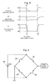
- Fig. 7 is a circuit configuration view of principal parts of the high-voltage power unit, and waveform charts (a), (b) and (c) in Fig. 8 are waveform charts illustrating change in a voltage in the case of switching the polarity in the high-voltage power unit.
- waveform charts (a), (b) and (c) in Fig. 8 With reference to Fig. 7 , and the waveform charts (a), (b) and (c) in Fig. 8 , a configuration and operation of the high-voltage power unit will schematically be described.
- a positive voltage generating circuit 2 includes a transformer T1 as a booster, a drive circuit 3 for driving a primary winding of the transformer T1, and a rectifier circuit using a Cockcroft-Walton circuit composed of four capacitors C1 through C4 and four diodes D1 through D4 connected to the secondary winding of the transformer T1.
- a negative voltage generating circuit 4 is similar in a basic configuration to the positive voltage generating circuit 2 except for the point that the direction of each of the diodes D5 through D8 in the Cockcroft-Walton circuit is opposite to that in the positive voltage generator 2.
- An output terminal P2 of the positive voltage generating circuit 2 and an output terminal Q1 of the negative voltage generating circuit 4 are connected.
- the other output terminal Q2 of the negative voltage generating circuit 4 is grounded via a resistor 9.
- a resistor 51 is connected in parallel.
- another resistor 52 is connected in parallel.
- a high voltage is output from the output terminal P1 of the positive voltage generating circuit 2 where the polarity is switched.
- a resistor 7 and a resistor 8 are connected in series. A voltage signal is fed back to a control circuit 1 from a junction point between the resistors 7 and 8.
- the drive circuits 3 and 5 each include a direct current voltage supply, which is connected in series to the primary winding of the transformer T1, and a switching element.
- the voltage applied from the direct current voltage supply to the primary winding (or a current to be supplied) is connected and disconnected by the switching element.
- the pulse width of a rectangular wave signal that performs ON/OFF driving of the switching element is controlled by the control circuit 1. Accordingly, the effective electric power supplied to the primary winding of the transformer T1 is changed, and consequently output voltages of the positive voltage generating circuit 2 and the negative voltage generating circuit 4 are changed.
- the control circuit 1 To output a positive high voltage +HV, the control circuit 1 sends a driving control signal only to the drive circuit 3 on the positive voltage generating circuit 2, so that only the positive voltage generating circuit 2 is operated and the negative voltage generating circuit 4 is stopped.
- the control circuit 1 since a voltage value corresponding to the voltage +HV appearing at the high-voltage output terminal is supplied to the control circuit 1 as a feedback, the control circuit 1 compares this voltage value with a target value, and regulates the driving control signal supplied to the drive circuit 3 in order to reduce the error. Accordingly, the output voltage +HV is precisely set to any target voltage.
- the control circuit 1 to output a negative high voltage, the control circuit 1 sends a driving control signal only to the drive circuit 5, so that only the negative voltage generating circuit 4 is operated while the positive voltage generating circuit 2 is stopped.
- the control circuit 1 controls each of the drive circuits 3 and 5 so that the output of the positive voltage generating circuit 2 changes from the voltage +HV to zero, while simultaneously the output of the negative voltage generating circuit 4 changes from zero and subside on a voltage -HV after an overshoot (see waveform charts (a) and (b) in Fig. 8 ).
- the output voltage changes in a short period of time.
- an overshot voltage needs to be fully settled (an overshoot needs to be terminated) before the next switching of the polarity is performed. This is because if the next polarity switching is performed before the overshoot is terminated, a fall of a high voltage after an overshoot is added to a next change (rise) in the high voltage in the direction identical to the fall, and thereby it takes a longer time before settling the voltage after all. Therefore, there is a theoretical limit, in the first place, on the attempt of increasing the polarity switching speed by increasing the overshoot.
- a unit including semiconductor switches which are bridge-connected as illustrated in Fig. 9 As a high-voltage power unit of a quite different type, there is also known a unit including semiconductor switches which are bridge-connected as illustrated in Fig. 9 .
- switches 21 and 23 are turned on while switches 22 and 24 are turned off for outputting a positive voltage +HV.
- the switches 22 and 24 are turned on while the switches 21 and 23 are turned off.
- the semiconductor switches 21 to 24 are each constructed to include a large number of FETs connected in series. The gate terminal of each of the FETs is driven via a pulse transformer having high insulation, and the like.
- the present invention has been made in order to solve such a problem, and an object of the present invention is to provide a high-voltage power unit capable of switching the polarity of an output voltage at high speed while suppressing the cost, and a mass spectrometer using the power unit.
- a first aspect of the present invention made to accomplish the above-stated object is a high-voltage power unit including, for selectively outputting a high voltage of positive or negative polarity: a positive voltage generating circuit for generating a positive high voltage; a negative voltage generating circuit for generating a negative high voltage; and a control circuit for controlling each of the positive high voltage generated by the positive voltage generating circuit and the negative high voltage generated by the negative voltage generating circuit, wherein one of a pair of output terminals of the positive voltage generating circuit is connected to one of a pair of output terminals of the negative voltage generating circuit to connect the two voltage generating circuits in a series connection, and one of two terminals of the series connection is used as a reference side while the other terminal is used to take out a high-voltage output whose polarity is switched, the high-voltage power unit further including: a) a first impedance-variable circuit section connected between the pair of output terminals of the positive voltage generating circuit; b) a second impedance-
- the number of stages may be any number, and the change may be either continuous or discontinuous (discrete). Accordingly, the first and second impedance-variable circuit sections may be switching circuits for changing the impedance in two stages of a substantially infinite and zero.
- a second aspect of the present invention made to accomplish the above-stated object is a high-voltage power unit, including, for selectively outputting a high voltage of positive or negative polarity: a positive voltage generating circuit for generating a positive high voltage; a negative voltage generating circuit for generating a negative high voltage; and a control circuit for controlling each of the positive high voltage generated by the positive voltage generating circuit and the negative high voltage generated by the negative voltage generating circuit, wherein one of a pair of output terminals of the positive voltage generating circuit is connected to one of a pair of output terminals of the negative voltage generating circuit to connect the two voltage generating circuits in a series connection, and one of two terminals of the series connection is used as a reference side while the other is used to take out a high-voltage output whose polarity is switched, the high-voltage power unit further including: a) a first current source disposed in between the pair of output terminals of the positive voltage generating circuit for supplying a variable current from a high voltage side to
- the positive voltage generating circuit and the negative voltage generating circuit may each include a booster transformer, and a rectifier circuit using a Cockcroft-Walton circuit connected to a secondary winding of the transformer.
- control circuit may control the positive voltage generating circuit and the negative voltage generating circuit, when switching the polarity of the high-voltage output between positive and negative, so that an output voltage of one of the voltage generating circuits changes from a first predetermined voltage to zero, while an output voltage of the other voltage generating circuit simultaneously changes from zero to a second predetermined voltage.
- control circuit may control the positive voltage generating circuit and the negative voltage generating circuit, when switching the polarity of the high-voltage output between positive and negative, so that an output voltage of one of the voltage generating circuits changes from a first predetermined voltage to zero, while an output voltage of the other voltage generating circuit simultaneously changes from zero to subside on a second predetermined voltage after an overshoot.
- the first and second impedance-variable circuit sections in the first aspect may each be a circuit using one or a plurality of FETs for example.
- a withstand voltage of the FETs normally, the withstand voltage of the FETs are approximately 1[kV], whereas an output voltage of the high-voltage power unit required for the mass spectrometer is approximately 10[kV] at a maximum
- a plurality of FETs may be connected in a series connection, and a voltage appearing at the pair of output terminals of the positive voltage generating circuit or the negative voltage generating circuit may be divided by resistors (i.e., the voltage value may substantially be lowered).
- the divided voltages may be given to the gate terminals of the respective FETs, and a signal from the first or second output driver is supplied to the gate terminal of one of the plurality of FETs in the series connections to change the impedance of the one FET.
- a current passing to each of the FETs in the series connection, including the one FET can be controlled.
- the FET whose gate terminal receives a signal from the first or second output driver may be regarded as a current source wherein a current to be supplied changes in response to the signal.
- this configuration also corresponds to the high-voltage power unit in the second aspect.
- the first and second impedance-variable circuit sections or the first and second current sources may be configured to include at least one bipolar transistor, and a current signal by the first or second output driver may be supplied to the base terminal of the transistor.
- the first impedance-variable circuit section connected between the pair of output terminals of the positive voltage generating circuit is substantially not in operation when a positive voltage is output. It operates for the first time when the polarity of an output voltage is switched from positive to negative and a voltage appears on the output terminal of the negative voltage generating circuit. Then, electric charges accumulated on the positive output terminal where the voltage decreases toward zero are discharged through the first impedance-variable circuit section. As a consequence, the positive voltage quickly falls.
- the second impedance-variable circuit section connected between the pair of output terminals of the negative voltage generating circuit is substantially not in operation when a negative voltage is output.
- the impedance between the pair of output terminals where the voltage changes to zero largely falls or a large current passes between the pair of output terminals when the polarity of the output voltage is switched. Accordingly, the voltage (absolute value) falls faster than that in the high-voltage power unit disclosed in Patent Literature 1. This makes it possible to switch the polarity of the output voltage at high speed while suppressing an overshoot amount of the voltage (absolute value) on the rising side.
- the impedance-variable circuit sections and/or the current sources are driven corresponding to the voltage output from the voltage generation circuit of the other polarity via the first and second output drivers, which eliminates the necessity of a complicated and expensive drive circuit, including a pulse transformer for driving the FETs and an isolation transformer, which was necessary in the unit disclosed in Patent Literature 2.
- the high-voltage power unit according to the present invention described in the foregoing may be used in various applications and apparatuses which need a positive high voltage and a negative high voltage in an alternative manner, and the high-voltage power unit is particularly suitable for a mass spectrometer.
- the high-voltage power unit may be used in an ion source and/or an ion detector in a mass spectrometer, which needs to switch the polarity of a high voltage in response to the polarity of the ions to be analyzed.
- the high-voltage power unit according to the present invention can switch the polarity of the output voltage at high speed.
- high-voltage power unit In the high-voltage power unit according to the present invention, high-speed switching of an output voltage between positive and negative polarities can be achieved while the cost can be suppressed to the utmost without increase as compared with the conventional unit. Consequently, in a mass spectrometer using the high-voltage power unit according to the present invention for example, a cycle time of alternate switching between positive ion detection and negative ion detection can be decreased, and mis-detection of ions, both positive and negative, can be reduced thereby.
- Fig. 1 is a schematic configuration diagram of principal part of the high-voltage power unit in the present embodiment.
- component members identical to those in the conventional high-voltage power unit illustrated in Fig. 7 are designated by identical reference numerals.
- a control circuit 1, a positive voltage generating circuit 2 and a negative voltage generating circuit 4 which include drive circuits 3 and 5, respectively, and a series connection circuit of resistors 7 and 8 are identical to each other.
- the high-voltage power unit of the present embodiment and the conventional unit are different in the following point. That is, in the conventional unit, the resistor 51 is connected between the output terminals P1 and P2 of the positive voltage generating circuit 2 and the resistor 52 is connected between the output terminals Q1 and Q2 of the negative voltage generating circuit 4, respectively.
- a polarity switching auxiliary section 6A which is different from a simple resistor, is connected to output terminals P1 and P2 of the positive voltage generating circuit 2 and to output terminals Q1 and Q2 of the negative voltage generating circuit 4.
- a parallel circuit made up of a series connection circuit of resistors 60 and 61 and a switching circuit 62, is connected between the output terminals P1 and P2 of the positive voltage generating circuit 2.
- a parallel circuit made up of a series connection circuit of resistors 63 and 64 and a switching circuit 65, is connected between the output terminals Q1 and Q2 of the negative voltage generating circuit 4.
- a signal taken from a junction point between the resistors 60 and 61 on a positive polarity side is input as an ON/OFF driving control signal for the switching circuit 65 on a negative polarity side.
- a signal taken from a junction point between the resistors 63 and 64 on the negative polarity side is input as an ON/OFF driving control signal for the switching circuit 62 on the positive polarity side.
- the positive voltage generating circuit 2 is now operated so that a positive high voltage +HV appears in between the output terminals P1 and P2, while the negative voltage generating circuit 4 is substantially in a stopped state so that a voltage between the output terminals P3 and P4 is approximately zero.
- a voltage which is equal to a division of the high voltage +HV by a ratio between resistance values of these resistors 60 and 61 is generated at the junction point of the resistors 60 and 61.
- This voltage is given to the switching circuit 65 on the opposite polarity side as a driving control signal, so that the switching circuit 65 is turned on and a line between the output terminals Q1 and Q2 of the negative voltage generating circuit 4 is put in a conductive state.
- the positive voltage generating circuit 2 When the polarity of the voltage is switched from positive to negative in this state, the positive voltage generating circuit 2 is stopped and the negative voltage generating circuit 4 is operated. The voltage between the output terminals P1 and P2 of the positive voltage generating circuit 2 starts to decrease. When the voltage decreases to a predetermined voltage, the switching circuit 65 is turned off, and the voltage (absolute value) between the output terminals Q1 and Q2 of the negative voltage generating circuit 4 conversely increases. Because of this increase, a driving control signal is given to the switching circuit 62 in this time, so that the switching circuit 62 is turned on. As a consequence, electric charges remaining in the output terminal P1 of the positive voltage generating circuit 2 is rapidly discharged through the switching circuit 62 and is quickly lowered to zero.
- the switching circuits 62 and 65 When the switching circuits 62 and 65 are turned on, the switching circuits 62 and 65 are in the state of being extremely low in the impedance so that current easily passes therethrough. Conversely, when the switching circuits 62 and 65 are turned off, the switching circuits 62 and 65 are in the state of being extremely high in the impedance so that current is hard to pass therethrough. That is, the switching circuits 62 and 65 may be regarded as impedance variable circuits in which an impedance largely changes corresponding to a voltage resistance-divided by the resistors 60 and 61 and the resistors 63 and 64.
- polarity switching auxiliary section 6A illustrated in Fig. 1 (and polarity switching auxiliary sections 6B, 6C, and 6D illustrated in Fig. 2A, Fig. 2B and Fig. 2C ) represents merely a principle configuration.
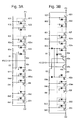
- Fig. 3A is a specific circuit configuration example of the polarity switching auxiliary section 6A.
- FETs are used as switching elements in the switching circuits 62 and 65.
- a typical drain terminal-source terminal withstand voltage of a FET is approximately 1[kV], and therefore when a high voltage of up to approximately ⁇ 10 [kV] is output, the withstand voltage of one FET cannot cover it.
- 10 or more FETs are connected in series, and in order to equalize voltages applied between drain terminals and source terminals of these FET 621 to 62n, a voltage between the output terminals P1 and P2 is divided by resistors 601 to 60n and 61 connected in series, and the divided voltages are each applied to the gate terminals of the FETs 621 to 62n.
- a resistor 62r is connected between the output terminal P2 and the source terminal of a FET 62n closest to the low-voltage side, among a large number of the FETs 621 to 62n connected in a series connection. Accordingly, the FET (hereinafter referred to as "drive FET" to distinguish this FET other FETs) 62n controls a current passing through other FETs 621 to 62m (determines the current value). The gate terminal of this FET 62n is connected to a junction point between a resistor 64n and a resistor 63 on the negative polarity side.
- a voltage obtained by resistance-dividing an output voltage on the negative polarity side is applied to the gate terminal of the FET 62n on the positive polarity side.
- the negative polarity side also has the same configuration. Zener diodes connected between the gate terminals and source terminals of all the FETs only function to prevent an overvoltage from being applied to the gate terminals.
- the output voltage (voltage between the output terminals Q1 and Q2) of the negative voltage generating circuit 4 is approximately zero, and therefore a current hardly passes to the drive FET 65n and other FETs 651 to 65m on the negative polarity side in actuality (that is, a current does not actually flow to the drive FET 65n and other FETs 651 to 65m though they have an ability to pass the current).
- a resistance value of the resistor 52 connected in parallel to the output terminals Q1 and Q2 is 50[M ⁇ ] and a capacitance of a capacitor in an output section is 100 [pF] when an output voltage is 10[kV].
- series connection circuits of FETs including the drive FETs 62n and 65n are equivalent to the first and second impedance-variable circuit sections in the present invention
- series connection circuits of resistors each including the resistors 60n and 61 and the resistors 64n and 63 for giving driving control signals to drive the drive FETs 62n and 65n are equivalent to the first and second output drivers in the present invention.
- the former i.e., the series connection circuits of FETs may also be regarded as a current source with a limited maximum current as described before.
- the series connection circuits of FETs including the drive FETs 62n and 65n may be regarded as first and second current sources in the present invention. Therefore, the polarity switching auxiliary section 6B of Fig. 2A , which represents a principle configuration different from that of the polarity switching auxiliary section 6A in Fig. 1 , may include the switching circuits 62 and 65 as variable current sources 68 and 69, respectively.
- both the polarity switching auxiliary sections 6A and 6B take out signals for driving the impedance variable circuits and the current sources from the voltages, they may take out the signals from currents.
- Fig. 2B and Fig. 2C are principle configuration diagrams of polarity switching auxiliary sections 6C and 6D using current drivers 66 and 67 for taking out current signals via resistors.
- Fig. 3B is a specific circuit configuration example of the polarity switching auxiliary sections 6C and 6D.
- a voltage appearing at the output terminals P1, P2, Q1, and Q2 of the positive and negative voltage generation circuits 2 and 4 is divided into voltages by a Zener diode 62y, the resistors 601 to 60n, and the resistors 641 to 64n, and these voltages are collectively applied to the gate terminals of the drive FETs 62n and 65n on the same polarity side.
- a current passing through the resistors 601 to 60n, and the resistors 641 to 64n provided for the voltage division is taken out via the resistors 61 and 63, and is supplied as a current signal to the base terminals of the bipolar transistors 62t and 65t, which are connected to the source terminals of the drive FETs 62n and 65n.
- the transistors 62t and 65t are turned on and off, and the drive FETs 62n and 65 are operated thereby.
- the drive FETs 62n and 65n are driven by the voltage in Fig. 3A
- the drive FETs 62n and 65n are driven by the current in Fig. 3B .
- the resistors 62r and 65r connected in series to the source terminals of the drive FETs 62n and 65n are set to 1[k ⁇ ]
- the resistors 62s and 65s are set to 1[M ⁇ ]
- the gate terminals of the drive FETs 62n and 65n are constantly charged regardless of the polarity of the voltage at the time of voltage output, so that the operation of the drive FETs 62n and 65n is quickly started and the voltage falls at high speed on the voltage OFF-side.
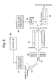
- Fig. 6 illustrates an example of the schematic configuration of a mass spectrometer using the high-voltage power unit according to the present embodiment.
- This mass spectrometer is used for analyzing a sample liquid eluted from a liquid chromatograph for example.
- the sample liquid is sprayed into an atmosphere of approximate atmospheric pressure from a nozzle 31 for an electrospray. This ionizes sample atoms and molecules contained in the sample liquid.
- high voltages normally, several [kV]
- a high-voltage power unit 37 of a polarity switching type as described earlier can be used.
- the ions generated by the aforementioned ionization are sent to a subsequent stage through a desolvation pipe 32, and are focused by an ion lens 33 driven by a voltage source, which is not illustrated, before being introduced into a space across the long axis of a quadrupole filter 34.
- a voltage in which an RF voltage and a DC voltage are superposed is applied to the quadrupole filter 34 by the voltage source which is not illustrated.
- the voltage forms an electric field, by which only ions having a predetermined mass number pass through the quadrupole filter 34.
- a high voltage (normally, approximately 10[kV]) with a polarity opposite to that of the ions to be analyzed is applied to a conversion dynode 35 in the further subsequent stage by a high-voltage power unit 38 of a polarity switching type as previously described.
- the ions induced by the electric field by the high voltage touch the conversion dynode 35 to emit secondary electrons.
- the emitted secondary electrons fly downward and reach a secondary electron multiplier 36. They are multiplied inside the secondary electron multiplier 36, and a detection signal corresponding to the number of the secondary electrons that flew in first, i.e. the number of the ions that reach the conversion dynode 35, is taken out.
- the controller 39 sends control signals for switching to each of the high-voltage power units 37 and 38 in accordance with the polarity of the ions to be analyzed. Since switching of the polarity of the output voltage in the high-voltage power units 37 and 38 can quickly be performed as described earlier, the time in which ion detection cannot be performed is decreased even in the case where, for example, positive ion detection and negative ion detection are repeatedly performed alternately every short period of time. Accordingly, fine mass chromatograms and total ion chromatograms can be created.
- Fig. 6 is an example of a simplified configuration. It is apparent that the previously-described high-voltage power unit of a polarity switching type may be used in a portion other than that described earlier.
- Fig. 4A, Fig. 4B , Fig. 5A and Fig. 5B show waveforms actually observed when the polarity is switched in each of the high-voltage power unit of the configuration illustrated in Fig. 3B and the conventional high-voltage power unit (conventional circuit).
- Fig. 4A and Fig. 4B illustrate voltage response waveforms at the time of switching the polarity of a voltage ( ⁇ 10[kV]) applied to a conversion dynode.
- Fig. 5A and Fig. 5B are ionic response waveforms at the time of switching the polarity of a voltage in order to switch the polarity of the ions to be measured in a mass spectrometer as illustrated in Fig. 6 . As illustrated in Fig.
- the high-voltage power unit according to the present invention is very effective for switching the polarity of the ions to be measured in a mass spectrometer.
- the high-voltage power unit described in the previously-described embodiment is merely an example of the present invention, and it is clear that any modifications, additions and adjustment to be made appropriately within the scope of the present invention are also embraced in the scope of the claims of the present application. It is also clearly understood that the high-voltage power unit according to the present invention is not only applicable to the mass spectrometers, but also to various applications and apparatuses which need to switch high voltages of approximately ⁇ several [kV] at high speed.
Landscapes
- Engineering & Computer Science (AREA)
- Power Engineering (AREA)
- Chemical & Material Sciences (AREA)
- Analytical Chemistry (AREA)
- Physics & Mathematics (AREA)
- Plasma & Fusion (AREA)
- Dc-Dc Converters (AREA)
- Electron Tubes For Measurement (AREA)
- Rectifiers (AREA)
- Other Investigation Or Analysis Of Materials By Electrical Means (AREA)
Abstract
Description
- The present invention relates to a high-voltage power unit capable of switching the polarity of an output voltage between positive and negative, and to a mass spectrometer using the power unit.
- Ion detectors including a combination of a conversion dynode and a secondary-electron multiplier are often used for detecting ions with high sensitivity in a mass spectrometer. In such an ion detector, a high voltage (± several [kV] to ± 10[kV] for example) having a polarity opposite to that of the ions to be analyzed is applied to a conversion dynode for selectively detecting positive ions and negative ions. In a liquid chromatograph mass spectrometer, an ion source according to an electrospray ionization (ESI) method, for example, is used for vaporizing and ionizing a liquid sample. In such an ion source, a high voltage (± several [kV] for example) with the same polarity as that of the ions to be analyzed is applied to the tip of a nozzle for spraying the liquid sample.
- In these applications, the polarity of the high voltage to be applied needs to be changed in response to the polarity of the ions to be analyzed. Therefore, a high-voltage power unit having an output voltage capable of switching the polarity of the output voltage is used. One of the most conventionally well-known high-voltage power units for switching high voltages of different polarities is one using a high-voltage reed relay (see, for example, Patent Literature 1).
- In a high-voltage power unit using a reed relay, when switching the polarity of the output voltage, spike discharges may occur to break the relay. In order to avoid such a situation, it is necessary to observe the following procedures: decrease the output voltage in one polarity, actuate the relay to change the contacts when the output voltage becomes adequately low, and after that, increase the output voltage in the other polarity. Consequently, it takes some time to switch the polarity. In the case where, for example, the detection of positive ions and negative ions are alternately switched every short period of time, the non-detection time increases in a mass spectrometer. This causes a problem of affecting the accuracy of an analysis.
- As a solution to such a problem, a high-voltage power unit capable of switching the polarity of an output voltage at high speed is disclosed in
Patent Literature 2.Fig. 7 is a circuit configuration view of principal parts of the high-voltage power unit, and waveform charts (a), (b) and (c) inFig. 8 are waveform charts illustrating change in a voltage in the case of switching the polarity in the high-voltage power unit. With reference toFig. 7 , and the waveform charts (a), (b) and (c) inFig. 8 , a configuration and operation of the high-voltage power unit will schematically be described. - In the high-voltage power unit, a positive voltage generating
circuit 2 includes a transformer T1 as a booster, adrive circuit 3 for driving a primary winding of the transformer T1, and a rectifier circuit using a Cockcroft-Walton circuit composed of four capacitors C1 through C4 and four diodes D1 through D4 connected to the secondary winding of the transformer T1. A negativevoltage generating circuit 4 is similar in a basic configuration to the positive voltage generatingcircuit 2 except for the point that the direction of each of the diodes D5 through D8 in the Cockcroft-Walton circuit is opposite to that in thepositive voltage generator 2. - An output terminal P2 of the positive
voltage generating circuit 2 and an output terminal Q1 of the negativevoltage generating circuit 4 are connected. The other output terminal Q2 of the negative voltage generatingcircuit 4 is grounded via aresistor 9. Between the output terminals P1 and P2 of the positive voltage generatingcircuit 2, aresistor 51 is connected in parallel. Between the output terminals Q1 and Q2 of the negative voltage generatingcircuit 4, anotherresistor 52 is connected in parallel. A high voltage is output from the output terminal P1 of the positivevoltage generating circuit 2 where the polarity is switched. Between this high-voltage output terminal and the ground, aresistor 7 and aresistor 8 are connected in series. A voltage signal is fed back to acontrol circuit 1 from a junction point between theresistors - The
drive circuits control circuit 1. Accordingly, the effective electric power supplied to the primary winding of the transformer T1 is changed, and consequently output voltages of the positivevoltage generating circuit 2 and the negativevoltage generating circuit 4 are changed. - To output a positive high voltage +HV, the
control circuit 1 sends a driving control signal only to thedrive circuit 3 on the positive voltage generatingcircuit 2, so that only the positivevoltage generating circuit 2 is operated and the negativevoltage generating circuit 4 is stopped. In this case, since a voltage value corresponding to the voltage +HV appearing at the high-voltage output terminal is supplied to thecontrol circuit 1 as a feedback, thecontrol circuit 1 compares this voltage value with a target value, and regulates the driving control signal supplied to thedrive circuit 3 in order to reduce the error. Accordingly, the output voltage +HV is precisely set to any target voltage. Contrary to the above case, to output a negative high voltage, thecontrol circuit 1 sends a driving control signal only to thedrive circuit 5, so that only the negative voltage generatingcircuit 4 is operated while the positivevoltage generating circuit 2 is stopped. - During a transition period wherein output of the positive high +HV is switched to output of a negative high voltage, the
control circuit 1 controls each of thedrive circuits circuit 2 changes from the voltage +HV to zero, while simultaneously the output of the negative voltage generatingcircuit 4 changes from zero and subside on a voltage -HV after an overshoot (see waveform charts (a) and (b) inFig. 8 ). Thus, by deliberately overshooting the voltage that changes from zero in this way, delay in a fall of the other voltage that returns to zero is compensated for. This makes it possible to quickly reach the target output voltage. Accordingly, the output voltage changes in a short period of time. - In recent years, to meet demands for further enhancement in throughput and higher temporal resolution in measurement in mass spectrometers, high-voltage power units are required to switch the polarity of an output voltage in higher speed. To further reduce the polarity switching time in the high-voltage power unit disclosed in
Patent Literature 2 stated above, it is necessary, for example, to further increase an overshoot of a negative voltage when a voltage is switched from positive to negative, or to increase the falling speed of a positive voltage (+HV to zero). To achieve the former, it is necessary to increase the voltage generation capability of the negativevoltage generating circuit 4. However, this entails such disadvantages as a significant cost hike of the circuits and an increase in necessary electric energy. To achieve the latter, it is necessary to reduce the resistance value of theresistor 51. However, this entails such disadvantages as an increased power loss in theresistor 51 and a necessity of using expensive resistors which can withstand large electric power. - In the high-voltage power unit, an overshot voltage needs to be fully settled (an overshoot needs to be terminated) before the next switching of the polarity is performed. This is because if the next polarity switching is performed before the overshoot is terminated, a fall of a high voltage after an overshoot is added to a next change (rise) in the high voltage in the direction identical to the fall, and thereby it takes a longer time before settling the voltage after all. Therefore, there is a theoretical limit, in the first place, on the attempt of increasing the polarity switching speed by increasing the overshoot.
- As a high-voltage power unit of a quite different type, there is also known a unit including semiconductor switches which are bridge-connected as illustrated in
Fig. 9 . In this high-voltage power unit,switches switches switches switches semiconductor switches 21 to 24 are each constructed to include a large number of FETs connected in series. The gate terminal of each of the FETs is driven via a pulse transformer having high insulation, and the like. However, in such a high-voltage power unit, a large number of pulse transformers are needed, and for driving each of these pulse transformers, drive circuits are also needed. Complicated drive control is also needed to prevent a pair ofswitches switches -
- [Patent Literature 1]
US 6,002,600 A (seeFig. 1C ) - [Patent Literature 2]
JP 4687716 B - It is difficult for the aforementioned conventional high-voltage power units to switch the polarity of a high voltage of kV order at speed further higher than before in a relatively inexpensive configuration (practically without a considerable cost hike as compared with the unit disclosed in Patent Literature 2).
- The present invention has been made in order to solve such a problem, and an object of the present invention is to provide a high-voltage power unit capable of switching the polarity of an output voltage at high speed while suppressing the cost, and a mass spectrometer using the power unit.
- A first aspect of the present invention made to accomplish the above-stated object is a high-voltage power unit including, for selectively outputting a high voltage of positive or negative polarity: a positive voltage generating circuit for generating a positive high voltage; a negative voltage generating circuit for generating a negative high voltage; and a control circuit for controlling each of the positive high voltage generated by the positive voltage generating circuit and the negative high voltage generated by the negative voltage generating circuit, wherein one of a pair of output terminals of the positive voltage generating circuit is connected to one of a pair of output terminals of the negative voltage generating circuit to connect the two voltage generating circuits in a series connection, and one of two terminals of the series connection is used as a reference side while the other terminal is used to take out a high-voltage output whose polarity is switched, the high-voltage power unit further including: a) a first impedance-variable circuit section connected between the pair of output terminals of the positive voltage generating circuit; b) a second impedance-variable circuit section connected between the pair of output terminals of the negative voltage generating circuit; c) a first output driver for driving the second impedance-variable circuit section to change an impedance of the second impedance variable circuit section based on a voltage or a current appearing on the pair of output terminals of the positive voltage generating circuit; and d) a second output driver for driving the first impedance-variable circuit section to change an impedance of the first impedance-variable circuit section based on a voltage or a current appearing on the pair of output terminals of the negative voltage generating circuit.
- As to the first and second impedance-variable circuit sections, as long as values of the impedance in the first and second impedance-variable circuit sections change in a plurality of stages in response to driving control signals by the second and first output drivers, the number of stages may be any number, and the change may be either continuous or discontinuous (discrete). Accordingly, the first and second impedance-variable circuit sections may be switching circuits for changing the impedance in two stages of a substantially infinite and zero.
- A second aspect of the present invention made to accomplish the above-stated object is a high-voltage power unit, including, for selectively outputting a high voltage of positive or negative polarity: a positive voltage generating circuit for generating a positive high voltage; a negative voltage generating circuit for generating a negative high voltage; and a control circuit for controlling each of the positive high voltage generated by the positive voltage generating circuit and the negative high voltage generated by the negative voltage generating circuit, wherein one of a pair of output terminals of the positive voltage generating circuit is connected to one of a pair of output terminals of the negative voltage generating circuit to connect the two voltage generating circuits in a series connection, and one of two terminals of the series connection is used as a reference side while the other is used to take out a high-voltage output whose polarity is switched, the high-voltage power unit further including: a) a first current source disposed in between the pair of output terminals of the positive voltage generating circuit for supplying a variable current from a high voltage side to a low voltage side, the variable current having a maximum current limited to a predetermined value; b) a second current source disposed in between the pair of output terminals of the negative voltage generating circuit for supplying a variable current from the high voltage side to the low voltage side, the variable current having a maximum current limited to a predetermined value; c) a first output driver for driving the second current source to change a current supplied from the second current source based on a voltage or a current appearing at the pair of output terminals of the positive voltage generating circuit; and d) a second output driver for driving the first current source to change a current supplied from the first current source based on a voltage or a current appearing at the pair of output terminals of the negative voltage generating circuit.
- In the first and second aspects, the positive voltage generating circuit and the negative voltage generating circuit may each include a booster transformer, and a rectifier circuit using a Cockcroft-Walton circuit connected to a secondary winding of the transformer.
- In the high-voltage power unit according to the present invention, the control circuit may control the positive voltage generating circuit and the negative voltage generating circuit, when switching the polarity of the high-voltage output between positive and negative, so that an output voltage of one of the voltage generating circuits changes from a first predetermined voltage to zero, while an output voltage of the other voltage generating circuit simultaneously changes from zero to a second predetermined voltage. More specifically, the control circuit may control the positive voltage generating circuit and the negative voltage generating circuit, when switching the polarity of the high-voltage output between positive and negative, so that an output voltage of one of the voltage generating circuits changes from a first predetermined voltage to zero, while an output voltage of the other voltage generating circuit simultaneously changes from zero to subside on a second predetermined voltage after an overshoot.
- The first and second impedance-variable circuit sections in the first aspect may each be a circuit using one or a plurality of FETs for example. When the absolute values of output voltages of the positive voltage generating circuit and the negative voltage generating circuit are beyond a withstand voltage of the FETs (normally, the withstand voltage of the FETs are approximately 1[kV], whereas an output voltage of the high-voltage power unit required for the mass spectrometer is approximately 10[kV] at a maximum), a plurality of FETs may be connected in a series connection, and a voltage appearing at the pair of output terminals of the positive voltage generating circuit or the negative voltage generating circuit may be divided by resistors (i.e., the voltage value may substantially be lowered). The divided voltages may be given to the gate terminals of the respective FETs, and a signal from the first or second output driver is supplied to the gate terminal of one of the plurality of FETs in the series connections to change the impedance of the one FET. As a result, a current passing to each of the FETs in the series connection, including the one FET, can be controlled.
- For example, as described in the foregoing, among the plurality of FETs in the series connection, the FET whose gate terminal receives a signal from the first or second output driver may be regarded as a current source wherein a current to be supplied changes in response to the signal. In short, this configuration also corresponds to the high-voltage power unit in the second aspect.
- When a signal by the first or second output driver is a current signal, the first and second impedance-variable circuit sections or the first and second current sources may be configured to include at least one bipolar transistor, and a current signal by the first or second output driver may be supplied to the base terminal of the transistor.
- In the first aspect, the first impedance-variable circuit section connected between the pair of output terminals of the positive voltage generating circuit is substantially not in operation when a positive voltage is output. It operates for the first time when the polarity of an output voltage is switched from positive to negative and a voltage appears on the output terminal of the negative voltage generating circuit. Then, electric charges accumulated on the positive output terminal where the voltage decreases toward zero are discharged through the first impedance-variable circuit section. As a consequence, the positive voltage quickly falls. The second impedance-variable circuit section connected between the pair of output terminals of the negative voltage generating circuit is substantially not in operation when a negative voltage is output. It operates for the first time when the polarity of the output voltage is switched from negative to positive and a voltage appears on the output terminal of the positive voltage generating circuit. Then, electric charges accumulated on the negative output terminal where the voltage (absolute value) decreases toward zero are discharged through the second impedance-variable circuit section. As a consequence, the negative voltage (absolute value) quickly falls.
- Thus, in the high-voltage power unit according to the present invention, the impedance between the pair of output terminals where the voltage changes to zero largely falls or a large current passes between the pair of output terminals when the polarity of the output voltage is switched. Accordingly, the voltage (absolute value) falls faster than that in the high-voltage power unit disclosed in
Patent Literature 1. This makes it possible to switch the polarity of the output voltage at high speed while suppressing an overshoot amount of the voltage (absolute value) on the rising side. The impedance-variable circuit sections and/or the current sources are driven corresponding to the voltage output from the voltage generation circuit of the other polarity via the first and second output drivers, which eliminates the necessity of a complicated and expensive drive circuit, including a pulse transformer for driving the FETs and an isolation transformer, which was necessary in the unit disclosed inPatent Literature 2. - The high-voltage power unit according to the present invention described in the foregoing may be used in various applications and apparatuses which need a positive high voltage and a negative high voltage in an alternative manner, and the high-voltage power unit is particularly suitable for a mass spectrometer. Specifically, the high-voltage power unit may be used in an ion source and/or an ion detector in a mass spectrometer, which needs to switch the polarity of a high voltage in response to the polarity of the ions to be analyzed. As described in the foregoing, the high-voltage power unit according to the present invention can switch the polarity of the output voltage at high speed. Accordingly, in the case of, for example, alternately performing detection of positive ions and detection of negative ion every short period of time, it is possible to decrease a non-detection period in which both positive and negative ions cannot be detected, and to thereby reduce undetected ions.
- In the high-voltage power unit according to the present invention, high-speed switching of an output voltage between positive and negative polarities can be achieved while the cost can be suppressed to the utmost without increase as compared with the conventional unit. Consequently, in a mass spectrometer using the high-voltage power unit according to the present invention for example, a cycle time of alternate switching between positive ion detection and negative ion detection can be decreased, and mis-detection of ions, both positive and negative, can be reduced thereby.
-
-
Fig. 1 is a schematic configuration diagram of principle part of a high-voltage power unit according to an embodiment of the present invention. -
Fig. 2A, Fig. 2B and Fig. 2C illustrate other configuration examples of a polarity switching auxiliary section inFig. 1 . -
Fig. 3A and Fig. 3B illustrate detailed circuit examples of the polarity switching auxiliary sections illustrated inFig. 1 ,Fig. 2A, Fig. 2B and Fig. 2C . -
Fig. 4A and Fig. 4B are a schematic configuration diagram of a mass spectrometer using the high-voltage power unit of the present embodiment. -
Fig. 5A and Fig. 5B are waveform charts of output voltages observed when the polarity is switched in each of the high-voltage power unit of the present embodiment and the conventional high-voltage power unit disclosed inPatent Literature 1. -
Fig. 6 is waveform charts of an ionic response observed in the case of applying the high-voltage power unit of the present embodiment and the conventional high-voltage power unit to a mass spectrometer. -
Fig. 7 is a configuration diagram of principal part of the conventional high-voltage power unit disclosed inPatent Literature 1. -
Fig. 8 shows waveform charts (a), (b) and (c) for describing the operation at the time of switching the polarity of an output voltage in the conventional high-voltage power unit. -
Fig. 9 is a schematic configuration diagram of principal part of another conventional high-voltage power unit. - Hereinafter, one embodiment of a high-voltage power unit according to the present invention will be described in detail in reference to
Fig.1 through Fig. 3A andFig. 3B .Fig. 1 is a schematic configuration diagram of principal part of the high-voltage power unit in the present embodiment. InFig. 1 , component members identical to those in the conventional high-voltage power unit illustrated inFig. 7 are designated by identical reference numerals. - As is clear from comparison between
Fig. 1 andFig. 7 , acontrol circuit 1, a positivevoltage generating circuit 2 and a negativevoltage generating circuit 4 which includedrive circuits resistors resistor 51 is connected between the output terminals P1 and P2 of the positivevoltage generating circuit 2 and theresistor 52 is connected between the output terminals Q1 and Q2 of the negativevoltage generating circuit 4, respectively. In the unit of the present embodiment, a polarity switchingauxiliary section 6A, which is different from a simple resistor, is connected to output terminals P1 and P2 of the positivevoltage generating circuit 2 and to output terminals Q1 and Q2 of the negativevoltage generating circuit 4. - In the polarity switching
auxiliary section 6A, a parallel circuit, made up of a series connection circuit ofresistors switching circuit 62, is connected between the output terminals P1 and P2 of the positivevoltage generating circuit 2. A parallel circuit, made up of a series connection circuit ofresistors switching circuit 65, is connected between the output terminals Q1 and Q2 of the negativevoltage generating circuit 4. A signal taken from a junction point between theresistors circuit 65 on a negative polarity side. Conversely, a signal taken from a junction point between theresistors circuit 62 on the positive polarity side. - A schematic description will be given of the operation at the time of switching the polarity of an output voltage in the high-voltage power unit of the present embodiment. For example, assume that the positive
voltage generating circuit 2 is now operated so that a positive high voltage +HV appears in between the output terminals P1 and P2, while the negativevoltage generating circuit 4 is substantially in a stopped state so that a voltage between the output terminals P3 and P4 is approximately zero. In this case, a voltage which is equal to a division of the high voltage +HV by a ratio between resistance values of theseresistors resistors circuit 65 on the opposite polarity side as a driving control signal, so that the switchingcircuit 65 is turned on and a line between the output terminals Q1 and Q2 of the negativevoltage generating circuit 4 is put in a conductive state. - When the polarity of the voltage is switched from positive to negative in this state, the positive
voltage generating circuit 2 is stopped and the negativevoltage generating circuit 4 is operated. The voltage between the output terminals P1 and P2 of the positivevoltage generating circuit 2 starts to decrease. When the voltage decreases to a predetermined voltage, the switchingcircuit 65 is turned off, and the voltage (absolute value) between the output terminals Q1 and Q2 of the negativevoltage generating circuit 4 conversely increases. Because of this increase, a driving control signal is given to the switchingcircuit 62 in this time, so that the switchingcircuit 62 is turned on. As a consequence, electric charges remaining in the output terminal P1 of the positivevoltage generating circuit 2 is rapidly discharged through the switchingcircuit 62 and is quickly lowered to zero. - When the switching
circuits circuits circuits circuits circuits resistors resistors - The polarity switching
auxiliary section 6A illustrated inFig. 1 (and polarity switchingauxiliary sections Fig. 2A, Fig. 2B and Fig. 2C ) represents merely a principle configuration.Fig. 3A is a specific circuit configuration example of the polarity switchingauxiliary section 6A. In this example, FETs are used as switching elements in the switchingcircuits FET 621 to 62n, a voltage between the output terminals P1 and P2 is divided byresistors 601 to 60n and 61 connected in series, and the divided voltages are each applied to the gate terminals of theFETs 621 to 62n. - A
resistor 62r is connected between the output terminal P2 and the source terminal of aFET 62n closest to the low-voltage side, among a large number of theFETs 621 to 62n connected in a series connection. Accordingly, the FET (hereinafter referred to as "drive FET" to distinguish this FET other FETs) 62n controls a current passing throughother FETs 621 to 62m (determines the current value). The gate terminal of thisFET 62n is connected to a junction point between aresistor 64n and aresistor 63 on the negative polarity side. In short, a voltage obtained by resistance-dividing an output voltage on the negative polarity side is applied to the gate terminal of theFET 62n on the positive polarity side. The negative polarity side also has the same configuration. Zener diodes connected between the gate terminals and source terminals of all the FETs only function to prevent an overvoltage from being applied to the gate terminals. - Assume the state where a positive high voltage is currently output. In this case, since the output voltage of the negative
voltage generating circuit 4 is zero, the voltage at the gate terminal of thedrive FET 62n on the positive polarity side is approximately zero. Meanwhile, a voltage obtained by resistance-dividing the output voltage on the positive polarity side is applied to the gate terminal of thedrive FET 65n on the negative polarity side. For example, assume that the voltage obtained by resistance-dividing is 10[V], a resistance value of theresistor 65r connected to the source terminal of thedrive FET 65n is 1[kΩ], and a gate threshold value (Vth) of thedrive FET 65n is 4[V]. In this case, a current of (10[V]-4[V])/1[kΩ]=6[mA] max may pass to thedrive FET 65n andother FETs 651 to 65m in the series connection. However, at the time of outputting a positive voltage, the output voltage (voltage between the output terminals Q1 and Q2) of the negativevoltage generating circuit 4 is approximately zero, and therefore a current hardly passes to thedrive FET 65n andother FETs 651 to 65m on the negative polarity side in actuality (that is, a current does not actually flow to thedrive FET 65n andother FETs 651 to 65m though they have an ability to pass the current). - On the contrary, when a negative high voltage outputting state is switched to a positive high voltage outputting state, and a voltage between the output terminals P1 and P2 of the positive
voltage generating circuit 2 is in the middle of rising, a current of up to 6[mA] passes to thedrive FET 65n andother FETs 651 to 65m since electric charges are accumulated at the output of the negativevoltage generating circuit 4. As a consequence, the accumulated electric charges are quickly discharged. - As a comparison with the configuration of the present embodiment, the case of the conventional high-voltage power unit illustrated in
Fig. 7 is considered. - For example, assume that a resistance value of the
resistor 52 connected in parallel to the output terminals Q1 and Q2 is 50[MΩ] and a capacitance of a capacitor in an output section is 100 [pF] when an output voltage is 10[kV]. In this case, the voltage on the voltage OFF-side at the time of polarity switching decreases by a time constant of τ=50[MΩ]·100[pF]=5[ms]. When a voltage fall time tf is tf=3τ, tf=15[ms] is obtained. In comparison, in the high-voltage power unit of the present embodiment, when the output voltage and the capacitance of capacitor in the output section are similarly 10[kV] and 100[pF], respectively, tf=dt=C·dv/i=100[pF]·10[kV]/6[mA]=0.17[ms] is obtained from Q=CV. That is, while the conventional high-voltage power unit takes 15[ms] for a fall of a voltage on the voltage OFF-side at the time of switching the polarity of the output voltage, the high-voltage power unit of the present embodiment takes 0.17[ms] for a fall of the voltage on the voltage OFF-side, so that a considerable reduction in the fall time is achieved. - In the circuit illustrated in
Fig. 3A which embodies the polarity switchingauxiliary section 6A illustrated inFig. 1 , series connection circuits of FETs including thedrive FETs resistors resistors drive FETs drive FETs auxiliary section 6B ofFig. 2A , which represents a principle configuration different from that of the polarity switchingauxiliary section 6A inFig. 1 , may include the switchingcircuits current sources - Although both the polarity switching
auxiliary sections Fig. 2B and Fig. 2C are principle configuration diagrams of polarity switchingauxiliary sections current drivers Fig. 3B is a specific circuit configuration example of the polarity switchingauxiliary sections - In the circuit example of
Fig. 3B , a voltage appearing at the output terminals P1, P2, Q1, and Q2 of the positive and negativevoltage generation circuits Zener diode 62y, theresistors 601 to 60n, and theresistors 641 to 64n, and these voltages are collectively applied to the gate terminals of thedrive FETs resistors 601 to 60n, and theresistors 641 to 64n provided for the voltage division is taken out via theresistors bipolar transistors 62t and 65t, which are connected to the source terminals of thedrive FETs transistors 62t and 65t are turned on and off, and thedrive FETs drive FETs Fig. 3A , thedrive FETs Fig. 3B . - For example, the
resistors drive FETs resistors bipolar transistors 62t and 65t are connected in parallel to theseresistors drive FETs drive FETs transistors 62t and 65t are turned off. When thetransistors 62t and 65t are turned on, a current of (10[V]-4[V])/1[kΩ]=6[mA] max passes. Therefore, in the configuration ofFig. 3B , like the configuration ofFig. 3A described before, it is possible to increase the speed of a fall of a voltage on the voltage OFF-side when the polarity of an output voltage is switched, and to thereby achieve swift polarity switching. - When the circuit of
Fig. 3A is compared with the circuit ofFig. 3B , the latter is more advantageous in terms of the speed increase. This is because in the configuration ofFig. 3A , the gate terminals of thedrive FETs drive FETs Fig. 3B , the gate terminals of thedrive FETs drive FETs -
Fig. 6 illustrates an example of the schematic configuration of a mass spectrometer using the high-voltage power unit according to the present embodiment. This mass spectrometer is used for analyzing a sample liquid eluted from a liquid chromatograph for example. The sample liquid is sprayed into an atmosphere of approximate atmospheric pressure from anozzle 31 for an electrospray. This ionizes sample atoms and molecules contained in the sample liquid. In this process, high voltages (normally, several [kV]) with different polarities according to the polarity of the ions to be generated are to be applied to the tip of thenozzle 31. As a voltage source therefor, a high-voltage power unit 37 of a polarity switching type as described earlier can be used. - The ions generated by the aforementioned ionization are sent to a subsequent stage through a
desolvation pipe 32, and are focused by anion lens 33 driven by a voltage source, which is not illustrated, before being introduced into a space across the long axis of aquadrupole filter 34. A voltage in which an RF voltage and a DC voltage are superposed is applied to thequadrupole filter 34 by the voltage source which is not illustrated. The voltage forms an electric field, by which only ions having a predetermined mass number pass through thequadrupole filter 34. A high voltage (normally, approximately 10[kV]) with a polarity opposite to that of the ions to be analyzed is applied to aconversion dynode 35 in the further subsequent stage by a high-voltage power unit 38 of a polarity switching type as previously described. The ions induced by the electric field by the high voltage touch theconversion dynode 35 to emit secondary electrons. The emitted secondary electrons fly downward and reach asecondary electron multiplier 36. They are multiplied inside thesecondary electron multiplier 36, and a detection signal corresponding to the number of the secondary electrons that flew in first, i.e. the number of the ions that reach theconversion dynode 35, is taken out. - That is, in the mass spectrometer with the previously-described configuration, the
controller 39 sends control signals for switching to each of the high-voltage power units voltage power units -
Fig. 6 is an example of a simplified configuration. It is apparent that the previously-described high-voltage power unit of a polarity switching type may be used in a portion other than that described earlier. -
Fig. 4A, Fig. 4B ,Fig. 5A and Fig. 5B show waveforms actually observed when the polarity is switched in each of the high-voltage power unit of the configuration illustrated inFig. 3B and the conventional high-voltage power unit (conventional circuit).Fig. 4A and Fig. 4B illustrate voltage response waveforms at the time of switching the polarity of a voltage (±10[kV]) applied to a conversion dynode.Fig. 5A and Fig. 5B are ionic response waveforms at the time of switching the polarity of a voltage in order to switch the polarity of the ions to be measured in a mass spectrometer as illustrated inFig. 6 . As illustrated inFig. 4A and Fig. 4B , about 14[ms] is needed to switch the polarity in the conventional circuit, whereas in the present invention circuit, the polarity switching time is reduced to approximately 3[ms]. As illustrated inFig. 5A and Fig. 5B , in the present invention circuit, the speed of switching the polarity of a voltage is increased, so that a rising speed of the ion detecting signal is also drastically increased. - The above-stated observed results indicate that the high-voltage power unit according to the present invention is very effective for switching the polarity of the ions to be measured in a mass spectrometer.
- The configurations of the high-voltage power unit described in the previously-described embodiment is merely an example of the present invention, and it is clear that any modifications, additions and adjustment to be made appropriately within the scope of the present invention are also embraced in the scope of the claims of the present application. It is also clearly understood that the high-voltage power unit according to the present invention is not only applicable to the mass spectrometers, but also to various applications and apparatuses which need to switch high voltages of approximately ± several [kV] at high speed.
-
- 1 ... Control Circuit
- 2 ... Positive Voltage Generating Circuit
- 4 ... Negative Voltage Generating Circuit
- 3, 5 ... Drive Circuit
- C1-C8 ... Capacitors
- D1-D8 ... Diode
- T1, T2 ... Transformer
- P1, P2, Q1, Q2 ... Output Terminal
- 10 ... Resistor
- 31 ... Nozzle
- 32 ... Desolvation Pipe
- 33 ... Ion Lens
- 34 ... Quadrupole Filter
- 35 ... Conversion Dynode
- 36 ... Secondary Electron Multiplier
- 37 ... High-voltage Power Unit
- 38 ... High-voltage Power Unit
- 39 ... Controller
- 60, 61, 601-60n, 62r, 62s, 63, 64, 641-64n, 65r, 65s, 7, 8, 9 ... Resistor
- 62, 65 ... Switching Circuit
- 621-62m, 651-65m ... FET
- 62n, 65n ... Drive FET
- 62t, 65t ... Bipolar Transistor
- 62y ... Zener Diode
- 66, 67 ... Current Driver
- 68, 69 ... Variable Current Source
- 6A, 6B, 6C, 6D ... Polarity Switching Auxiliary Section
Claims (6)
- A high-voltage power unit, comprising, for selectively outputting a high voltage of positive or negative polarity:a positive voltage generating circuit for generating a positive high voltage;a negative voltage generating circuit for generating a negative high voltage; anda control circuit for controlling each of the positive high voltage generated by the positive voltage generating circuit and the negative high voltage generated by the negative voltage generating circuit, whereinone of a pair of output terminals of the positive voltage generating circuit is connected to one of a pair of output terminals of the negative voltage generating circuit to connect the two voltage generating circuits in a series connection, andone of two terminals of the series connection is used as a reference side, while the other terminal is used to take out a high-voltage output whose polarity is switched,the high-voltage power unit further comprising:a) a first impedance-variable circuit section connected between the pair of output terminals of the positive voltage generating circuit;b) a second impedance-variable circuit section connected between the pair of output terminals of the negative voltage generating circuit;c) a first output driver for driving the second impedance variable circuit section to change an impedance of the second impedance-variable circuit section based on a voltage or a current appearing at the pair of output terminals of the positive voltage generating circuit; andd) a second output driver for driving the first impedance-variable circuit section to change an impedance of the first impedance-variable circuit section based on a voltage or a current appearing at the pair of output terminals of the negative voltage generating circuit.
- A high-voltage power unit, comprising, for selectively outputting a high voltage of positive or negative polarity:a positive voltage generating circuit for generating a positive high voltage;a negative voltage generating circuit for generating a negative high voltage; anda control circuit for controlling each of the positive high voltage generated by the positive voltage generating circuit and the negative high voltage generated by the negative voltage generating circuit, whereinone of a pair of output terminals of the positive voltage generating circuit is connected to one of a pair of output terminals of the negative voltage generating circuit to connect the two voltage generating circuits in a series connection, andone of two terminals of the series connection is used as a reference side, while the other terminal is used to take out a high-voltage output whose polarity is switched,the high-voltage power unit further comprising:a) a first current source disposed in between the pair of output terminals of the positive voltage generating circuit for supplying a variable current from a high voltage side to a low voltage side, the variable current having a maximum current limited to a predetermined value;b) a second current source disposed in between the pair of output terminals of the negative voltage generating circuit for supplying a variable current from the high voltage side to the low voltage side, the variable current having a maximum current limited to a predetermined value;c) a first output driver for driving the second current source to change a current supplied from the second current source based on a voltage or a current appearing on the pair of output terminals of the positive voltage generating circuit; andd) a second output driver for driving the first current source to change a current supplied from the first current source based on a voltage or a current appearing on the pair of output terminals of the negative voltage generating circuit.
- The high-voltage power unit according to claim 1, wherein
the first and second impedance-variable circuit sections each include: drive FETs that are ON/OFF driven by the first and second output drivers; and a plurality of FETs connected in series to the drive FETs. - The high-voltage power unit according to claim 2, wherein
the first and second current sources each include: drive FETs that are ON/OFF driven by the first and second output drivers; and a plurality of FETs connected in series to the drive FETs. - The high-voltage power unit according to any one of claims 1 through 4, wherein
the control circuit controls the positive voltage generating circuit and the negative voltage generating circuit, when switching the polarity of the high-voltage output between positive and negative, so that an output voltage of one of the voltage generating circuits changes from a first predetermined voltage to zero while simultaneously an output voltage of the other voltage generating circuit changes from zero to subside on a second predetermined voltage after an overshoot. - A mass spectrometer using a high-voltage output by the high-voltage power unit according to any one of claims 1 through 5 in an ion source and/or an ion detector, wherein
a polarity of the high-voltage output by the high-voltage power unit is switched corresponding to a polarity of ions to be analyzed.
Applications Claiming Priority (1)
| Application Number | Priority Date | Filing Date | Title |
|---|---|---|---|
| PCT/JP2012/078595 WO2014068780A1 (en) | 2012-11-05 | 2012-11-05 | High voltage power supply apparatus and mass spectrometer using same |
Publications (3)
| Publication Number | Publication Date |
|---|---|
| EP2913914A1 true EP2913914A1 (en) | 2015-09-02 |
| EP2913914A4 EP2913914A4 (en) | 2016-05-11 |
| EP2913914B1 EP2913914B1 (en) | 2019-08-21 |
Family
ID=50626743
Family Applications (1)
| Application Number | Title | Priority Date | Filing Date |
|---|---|---|---|
| EP12887817.0A Active EP2913914B1 (en) | 2012-11-05 | 2012-11-05 | High voltage power supply apparatus and mass spectrometer using same |
Country Status (5)
| Country | Link |
|---|---|
| US (1) | US9431226B2 (en) |
| EP (1) | EP2913914B1 (en) |
| JP (1) | JP5822031B2 (en) |
| CN (1) | CN104769830B (en) |
| WO (1) | WO2014068780A1 (en) |
Cited By (11)
| Publication number | Priority date | Publication date | Assignee | Title |
|---|---|---|---|---|
| EP3211781A4 (en) * | 2014-10-20 | 2017-11-22 | Shimadzu Corporation | Mass spectroscope |
| GB2576077A (en) * | 2018-05-31 | 2020-02-05 | Micromass Ltd | Mass spectrometer |
| US11355331B2 (en) | 2018-05-31 | 2022-06-07 | Micromass Uk Limited | Mass spectrometer |
| US11373849B2 (en) | 2018-05-31 | 2022-06-28 | Micromass Uk Limited | Mass spectrometer having fragmentation region |
| US11437226B2 (en) | 2018-05-31 | 2022-09-06 | Micromass Uk Limited | Bench-top time of flight mass spectrometer |
| US11476103B2 (en) | 2018-05-31 | 2022-10-18 | Micromass Uk Limited | Bench-top time of flight mass spectrometer |
| US11538676B2 (en) | 2018-05-31 | 2022-12-27 | Micromass Uk Limited | Mass spectrometer |
| US11621154B2 (en) | 2018-05-31 | 2023-04-04 | Micromass Uk Limited | Bench-top time of flight mass spectrometer |
| US11879470B2 (en) | 2018-05-31 | 2024-01-23 | Micromass Uk Limited | Bench-top time of flight mass spectrometer |
| US12009193B2 (en) | 2018-05-31 | 2024-06-11 | Micromass Uk Limited | Bench-top Time of Flight mass spectrometer |
| US12027359B2 (en) | 2018-05-31 | 2024-07-02 | Micromass Uk Limited | Bench-top Time of Flight mass spectrometer |
Families Citing this family (11)
| Publication number | Priority date | Publication date | Assignee | Title |
|---|---|---|---|---|
| WO2016017045A1 (en) | 2014-07-28 | 2016-02-04 | ネッパジーン株式会社 | Electric pulse generator for electroporator, and electroporator system provided with electric pulse generator |
| JP6337970B2 (en) * | 2014-09-17 | 2018-06-06 | 株式会社島津製作所 | Mass spectrometer |
| WO2017145334A1 (en) * | 2016-02-25 | 2017-08-31 | 株式会社日立ハイテクノロジーズ | Power supply and mass spectrometer |
| JP6516062B2 (en) * | 2016-02-26 | 2019-05-22 | 株式会社島津製作所 | DC high voltage power supply |
| EP3525231A4 (en) * | 2016-10-04 | 2020-05-20 | Shimadzu Corporation | HIGH VOLTAGE POWER SUPPLY DEVICE |
| US10984998B2 (en) | 2017-10-26 | 2021-04-20 | Shimadzu Corporation | Mass spectrometer |
| CN108092495A (en) * | 2017-12-30 | 2018-05-29 | 聚光科技(杭州)股份有限公司 | Polarity of voltage switching device and method |
| EP3763029A4 (en) * | 2018-03-07 | 2021-11-10 | The Board of Trustees of the Leland Stanford Junior University | DEVICES AND METHODS WITH POWER CONVERSION WITH MULTIPLE RECTIFIER CIRCUITS |
| JP7592476B2 (en) * | 2020-12-07 | 2024-12-02 | キヤノン株式会社 | Power supply device and image forming apparatus |
| JP7563344B2 (en) * | 2021-09-08 | 2024-10-08 | 株式会社島津製作所 | High voltage power supply |
| CN120453151A (en) * | 2025-05-09 | 2025-08-08 | 欧陆分析测试技术服务(广州)有限公司 | Inductively Coupled Plasma Mass Spectrometry System with Intelligent Data Processing and Report Generation |
Family Cites Families (14)
| Publication number | Priority date | Publication date | Assignee | Title |
|---|---|---|---|---|
| US2397560A (en) * | 1943-08-18 | 1946-04-02 | Cons Eng Corp | Mass spectrometry |
| US4103324A (en) * | 1976-12-22 | 1978-07-25 | Airco, Inc. | Saturable reactor-type power supply |
| JPS61296650A (en) * | 1985-06-25 | 1986-12-27 | Anelva Corp | Power source for quadrupole type mass analyzer |
| GB9122598D0 (en) * | 1991-10-24 | 1991-12-04 | Fisons Plc | Power supply for multipolar mass filter |
| JP3372619B2 (en) * | 1993-12-15 | 2003-02-04 | キヤノン株式会社 | Image forming device |
| JPH06335247A (en) * | 1993-05-20 | 1994-12-02 | Canon Inc | Power supply |
| US6002600A (en) * | 1994-11-08 | 1999-12-14 | Spellman High Voltage Co. | Reversible polarity high voltage power supply |
| US6927985B2 (en) * | 2001-07-17 | 2005-08-09 | Newton Scientific, Inc. | High voltage generator |
| JP4133086B2 (en) | 2002-07-31 | 2008-08-13 | サンクス株式会社 | Static eliminator |
| JP2007066770A (en) * | 2005-08-31 | 2007-03-15 | Sunx Ltd | Static eliminator |
| US7855355B2 (en) | 2005-09-08 | 2010-12-21 | Shimadzu Corporation | High-voltage power unit and mass spectrometer using the power unit |
| GB0809950D0 (en) * | 2008-05-30 | 2008-07-09 | Thermo Fisher Scient Bremen | Mass spectrometer |
| DE202010006801U1 (en) * | 2010-05-14 | 2011-09-07 | Heike Kersten | charging generator |
| JP5508302B2 (en) * | 2011-01-21 | 2014-05-28 | 株式会社キーエンス | Static eliminator |
-
2012
- 2012-11-05 WO PCT/JP2012/078595 patent/WO2014068780A1/en not_active Ceased
- 2012-11-05 CN CN201280076873.XA patent/CN104769830B/en active Active
- 2012-11-05 JP JP2014544191A patent/JP5822031B2/en active Active
- 2012-11-05 EP EP12887817.0A patent/EP2913914B1/en active Active
- 2012-11-05 US US14/440,380 patent/US9431226B2/en active Active
Cited By (14)
| Publication number | Priority date | Publication date | Assignee | Title |
|---|---|---|---|---|
| EP3211781A4 (en) * | 2014-10-20 | 2017-11-22 | Shimadzu Corporation | Mass spectroscope |
| US10229822B2 (en) | 2014-10-20 | 2019-03-12 | Shimadzu Corporation | Mass spectrometer with high-voltage power source |
| GB2576077A (en) * | 2018-05-31 | 2020-02-05 | Micromass Ltd | Mass spectrometer |
| GB2576077B (en) * | 2018-05-31 | 2021-12-01 | Micromass Ltd | Mass spectrometer |
| US11355331B2 (en) | 2018-05-31 | 2022-06-07 | Micromass Uk Limited | Mass spectrometer |
| US11367607B2 (en) | 2018-05-31 | 2022-06-21 | Micromass Uk Limited | Mass spectrometer |
| US11373849B2 (en) | 2018-05-31 | 2022-06-28 | Micromass Uk Limited | Mass spectrometer having fragmentation region |
| US11437226B2 (en) | 2018-05-31 | 2022-09-06 | Micromass Uk Limited | Bench-top time of flight mass spectrometer |
| US11476103B2 (en) | 2018-05-31 | 2022-10-18 | Micromass Uk Limited | Bench-top time of flight mass spectrometer |
| US11538676B2 (en) | 2018-05-31 | 2022-12-27 | Micromass Uk Limited | Mass spectrometer |
| US11621154B2 (en) | 2018-05-31 | 2023-04-04 | Micromass Uk Limited | Bench-top time of flight mass spectrometer |
| US11879470B2 (en) | 2018-05-31 | 2024-01-23 | Micromass Uk Limited | Bench-top time of flight mass spectrometer |
| US12009193B2 (en) | 2018-05-31 | 2024-06-11 | Micromass Uk Limited | Bench-top Time of Flight mass spectrometer |
| US12027359B2 (en) | 2018-05-31 | 2024-07-02 | Micromass Uk Limited | Bench-top Time of Flight mass spectrometer |
Also Published As
| Publication number | Publication date |
|---|---|
| US9431226B2 (en) | 2016-08-30 |
| EP2913914A4 (en) | 2016-05-11 |
| JPWO2014068780A1 (en) | 2016-09-08 |
| CN104769830A (en) | 2015-07-08 |
| WO2014068780A1 (en) | 2014-05-08 |
| CN104769830B (en) | 2017-04-26 |
| JP5822031B2 (en) | 2015-11-24 |
| US20150287580A1 (en) | 2015-10-08 |
| EP2913914B1 (en) | 2019-08-21 |
Similar Documents
| Publication | Publication Date | Title |
|---|---|---|
| EP2913914B1 (en) | High voltage power supply apparatus and mass spectrometer using same | |
| JP6237924B2 (en) | Mass spectrometer | |
| US7855355B2 (en) | High-voltage power unit and mass spectrometer using the power unit | |
| JP6337970B2 (en) | Mass spectrometer | |
| EP3026807B1 (en) | High voltage power supply device and mass spectrometry device using same | |
| CN115776230B (en) | High-voltage power supply device | |
| US12087569B2 (en) | Time-of-flight mass spectrometry device and analysis method | |
| US11373851B2 (en) | High-voltage power supply device | |
| US11349476B2 (en) | High-voltage amplifier, high-voltage power supply, and mass spectrometer | |
| US20220262615A1 (en) | Analytical device |
Legal Events
| Date | Code | Title | Description |
|---|---|---|---|
| PUAI | Public reference made under article 153(3) epc to a published international application that has entered the european phase |
Free format text: ORIGINAL CODE: 0009012 |
|
| 17P | Request for examination filed |
Effective date: 20150529 |
|
| AK | Designated contracting states |
Kind code of ref document: A1 Designated state(s): AL AT BE BG CH CY CZ DE DK EE ES FI FR GB GR HR HU IE IS IT LI LT LU LV MC MK MT NL NO PL PT RO RS SE SI SK SM TR |
|
| AX | Request for extension of the european patent |
Extension state: BA ME |
|
| DAX | Request for extension of the european patent (deleted) | ||
| RA4 | Supplementary search report drawn up and despatched (corrected) |
Effective date: 20160408 |
|
| RIC1 | Information provided on ipc code assigned before grant |
Ipc: H02M 3/07 20060101ALI20160404BHEP Ipc: H02M 7/10 20060101AFI20160404BHEP Ipc: H02M 3/335 20060101ALI20160404BHEP Ipc: H01J 49/02 20060101ALI20160404BHEP Ipc: H02M 3/28 20060101ALI20160404BHEP Ipc: H02M 1/00 20060101ALI20160404BHEP |
|
| GRAP | Despatch of communication of intention to grant a patent |
Free format text: ORIGINAL CODE: EPIDOSNIGR1 |
|
| STAA | Information on the status of an ep patent application or granted ep patent |
Free format text: STATUS: GRANT OF PATENT IS INTENDED |
|
| INTG | Intention to grant announced |
Effective date: 20190328 |
|
| GRAS | Grant fee paid |
Free format text: ORIGINAL CODE: EPIDOSNIGR3 |
|
| GRAA | (expected) grant |
Free format text: ORIGINAL CODE: 0009210 |
|
| STAA | Information on the status of an ep patent application or granted ep patent |
Free format text: STATUS: THE PATENT HAS BEEN GRANTED |
|
| AK | Designated contracting states |
Kind code of ref document: B1 Designated state(s): AL AT BE BG CH CY CZ DE DK EE ES FI FR GB GR HR HU IE IS IT LI LT LU LV MC MK MT NL NO PL PT RO RS SE SI SK SM TR |
|
| REG | Reference to a national code |
Ref country code: GB Ref legal event code: FG4D |
|
| REG | Reference to a national code |
Ref country code: CH Ref legal event code: EP |
|
| REG | Reference to a national code |
Ref country code: DE Ref legal event code: R096 Ref document number: 602012063276 Country of ref document: DE |
|
| REG | Reference to a national code |
Ref country code: AT Ref legal event code: REF Ref document number: 1170872 Country of ref document: AT Kind code of ref document: T Effective date: 20190915 |
|
| REG | Reference to a national code |
Ref country code: IE Ref legal event code: FG4D |
|
| REG | Reference to a national code |
Ref country code: LT Ref legal event code: MG4D |
|
| REG | Reference to a national code |
Ref country code: NL Ref legal event code: MP Effective date: 20190821 |
|
| PG25 | Lapsed in a contracting state [announced via postgrant information from national office to epo] |
Ref country code: PT Free format text: LAPSE BECAUSE OF FAILURE TO SUBMIT A TRANSLATION OF THE DESCRIPTION OR TO PAY THE FEE WITHIN THE PRESCRIBED TIME-LIMIT Effective date: 20191223 Ref country code: BG Free format text: LAPSE BECAUSE OF FAILURE TO SUBMIT A TRANSLATION OF THE DESCRIPTION OR TO PAY THE FEE WITHIN THE PRESCRIBED TIME-LIMIT Effective date: 20191121 Ref country code: NL Free format text: LAPSE BECAUSE OF FAILURE TO SUBMIT A TRANSLATION OF THE DESCRIPTION OR TO PAY THE FEE WITHIN THE PRESCRIBED TIME-LIMIT Effective date: 20190821 Ref country code: LT Free format text: LAPSE BECAUSE OF FAILURE TO SUBMIT A TRANSLATION OF THE DESCRIPTION OR TO PAY THE FEE WITHIN THE PRESCRIBED TIME-LIMIT Effective date: 20190821 Ref country code: NO Free format text: LAPSE BECAUSE OF FAILURE TO SUBMIT A TRANSLATION OF THE DESCRIPTION OR TO PAY THE FEE WITHIN THE PRESCRIBED TIME-LIMIT Effective date: 20191121 Ref country code: HR Free format text: LAPSE BECAUSE OF FAILURE TO SUBMIT A TRANSLATION OF THE DESCRIPTION OR TO PAY THE FEE WITHIN THE PRESCRIBED TIME-LIMIT Effective date: 20190821 Ref country code: FI Free format text: LAPSE BECAUSE OF FAILURE TO SUBMIT A TRANSLATION OF THE DESCRIPTION OR TO PAY THE FEE WITHIN THE PRESCRIBED TIME-LIMIT Effective date: 20190821 Ref country code: SE Free format text: LAPSE BECAUSE OF FAILURE TO SUBMIT A TRANSLATION OF THE DESCRIPTION OR TO PAY THE FEE WITHIN THE PRESCRIBED TIME-LIMIT Effective date: 20190821 |
|
| PG25 | Lapsed in a contracting state [announced via postgrant information from national office to epo] |
Ref country code: IS Free format text: LAPSE BECAUSE OF FAILURE TO SUBMIT A TRANSLATION OF THE DESCRIPTION OR TO PAY THE FEE WITHIN THE PRESCRIBED TIME-LIMIT Effective date: 20191221 Ref country code: GR Free format text: LAPSE BECAUSE OF FAILURE TO SUBMIT A TRANSLATION OF THE DESCRIPTION OR TO PAY THE FEE WITHIN THE PRESCRIBED TIME-LIMIT Effective date: 20191122 Ref country code: RS Free format text: LAPSE BECAUSE OF FAILURE TO SUBMIT A TRANSLATION OF THE DESCRIPTION OR TO PAY THE FEE WITHIN THE PRESCRIBED TIME-LIMIT Effective date: 20190821 Ref country code: ES Free format text: LAPSE BECAUSE OF FAILURE TO SUBMIT A TRANSLATION OF THE DESCRIPTION OR TO PAY THE FEE WITHIN THE PRESCRIBED TIME-LIMIT Effective date: 20190821 Ref country code: AL Free format text: LAPSE BECAUSE OF FAILURE TO SUBMIT A TRANSLATION OF THE DESCRIPTION OR TO PAY THE FEE WITHIN THE PRESCRIBED TIME-LIMIT Effective date: 20190821 Ref country code: LV Free format text: LAPSE BECAUSE OF FAILURE TO SUBMIT A TRANSLATION OF THE DESCRIPTION OR TO PAY THE FEE WITHIN THE PRESCRIBED TIME-LIMIT Effective date: 20190821 |
|
| REG | Reference to a national code |
Ref country code: AT Ref legal event code: MK05 Ref document number: 1170872 Country of ref document: AT Kind code of ref document: T Effective date: 20190821 |
|
| PG25 | Lapsed in a contracting state [announced via postgrant information from national office to epo] |
Ref country code: TR Free format text: LAPSE BECAUSE OF FAILURE TO SUBMIT A TRANSLATION OF THE DESCRIPTION OR TO PAY THE FEE WITHIN THE PRESCRIBED TIME-LIMIT Effective date: 20190821 |
|
| PG25 | Lapsed in a contracting state [announced via postgrant information from national office to epo] |
Ref country code: RO Free format text: LAPSE BECAUSE OF FAILURE TO SUBMIT A TRANSLATION OF THE DESCRIPTION OR TO PAY THE FEE WITHIN THE PRESCRIBED TIME-LIMIT Effective date: 20190821 Ref country code: EE Free format text: LAPSE BECAUSE OF FAILURE TO SUBMIT A TRANSLATION OF THE DESCRIPTION OR TO PAY THE FEE WITHIN THE PRESCRIBED TIME-LIMIT Effective date: 20190821 Ref country code: DK Free format text: LAPSE BECAUSE OF FAILURE TO SUBMIT A TRANSLATION OF THE DESCRIPTION OR TO PAY THE FEE WITHIN THE PRESCRIBED TIME-LIMIT Effective date: 20190821 Ref country code: IT Free format text: LAPSE BECAUSE OF FAILURE TO SUBMIT A TRANSLATION OF THE DESCRIPTION OR TO PAY THE FEE WITHIN THE PRESCRIBED TIME-LIMIT Effective date: 20190821 Ref country code: AT Free format text: LAPSE BECAUSE OF FAILURE TO SUBMIT A TRANSLATION OF THE DESCRIPTION OR TO PAY THE FEE WITHIN THE PRESCRIBED TIME-LIMIT Effective date: 20190821 Ref country code: PL Free format text: LAPSE BECAUSE OF FAILURE TO SUBMIT A TRANSLATION OF THE DESCRIPTION OR TO PAY THE FEE WITHIN THE PRESCRIBED TIME-LIMIT Effective date: 20190821 |
|
| PG25 | Lapsed in a contracting state [announced via postgrant information from national office to epo] |
Ref country code: CZ Free format text: LAPSE BECAUSE OF FAILURE TO SUBMIT A TRANSLATION OF THE DESCRIPTION OR TO PAY THE FEE WITHIN THE PRESCRIBED TIME-LIMIT Effective date: 20190821 Ref country code: SK Free format text: LAPSE BECAUSE OF FAILURE TO SUBMIT A TRANSLATION OF THE DESCRIPTION OR TO PAY THE FEE WITHIN THE PRESCRIBED TIME-LIMIT Effective date: 20190821 Ref country code: IS Free format text: LAPSE BECAUSE OF FAILURE TO SUBMIT A TRANSLATION OF THE DESCRIPTION OR TO PAY THE FEE WITHIN THE PRESCRIBED TIME-LIMIT Effective date: 20200224 Ref country code: SM Free format text: LAPSE BECAUSE OF FAILURE TO SUBMIT A TRANSLATION OF THE DESCRIPTION OR TO PAY THE FEE WITHIN THE PRESCRIBED TIME-LIMIT Effective date: 20190821 |
|
| REG | Reference to a national code |
Ref country code: DE Ref legal event code: R097 Ref document number: 602012063276 Country of ref document: DE |
|
| REG | Reference to a national code |
Ref country code: CH Ref legal event code: PL |
|
| PLBE | No opposition filed within time limit |
Free format text: ORIGINAL CODE: 0009261 |
|
| STAA | Information on the status of an ep patent application or granted ep patent |
Free format text: STATUS: NO OPPOSITION FILED WITHIN TIME LIMIT |
|
| PG2D | Information on lapse in contracting state deleted |
Ref country code: IS |
|
| PG25 | Lapsed in a contracting state [announced via postgrant information from national office to epo] |
Ref country code: MC Free format text: LAPSE BECAUSE OF FAILURE TO SUBMIT A TRANSLATION OF THE DESCRIPTION OR TO PAY THE FEE WITHIN THE PRESCRIBED TIME-LIMIT Effective date: 20190821 Ref country code: LU Free format text: LAPSE BECAUSE OF NON-PAYMENT OF DUE FEES Effective date: 20191105 Ref country code: LI Free format text: LAPSE BECAUSE OF NON-PAYMENT OF DUE FEES Effective date: 20191130 Ref country code: CH Free format text: LAPSE BECAUSE OF NON-PAYMENT OF DUE FEES Effective date: 20191130 |
|
| 26N | No opposition filed |
Effective date: 20200603 |
|
| REG | Reference to a national code |
Ref country code: BE Ref legal event code: MM Effective date: 20191130 |
|
| PG25 | Lapsed in a contracting state [announced via postgrant information from national office to epo] |
Ref country code: SI Free format text: LAPSE BECAUSE OF FAILURE TO SUBMIT A TRANSLATION OF THE DESCRIPTION OR TO PAY THE FEE WITHIN THE PRESCRIBED TIME-LIMIT Effective date: 20190821 |
|
| PG25 | Lapsed in a contracting state [announced via postgrant information from national office to epo] |
Ref country code: IE Free format text: LAPSE BECAUSE OF NON-PAYMENT OF DUE FEES Effective date: 20191105 Ref country code: FR Free format text: LAPSE BECAUSE OF NON-PAYMENT OF DUE FEES Effective date: 20191130 |
|
| PG25 | Lapsed in a contracting state [announced via postgrant information from national office to epo] |
Ref country code: BE Free format text: LAPSE BECAUSE OF NON-PAYMENT OF DUE FEES Effective date: 20191130 |
|
| PG25 | Lapsed in a contracting state [announced via postgrant information from national office to epo] |
Ref country code: CY Free format text: LAPSE BECAUSE OF FAILURE TO SUBMIT A TRANSLATION OF THE DESCRIPTION OR TO PAY THE FEE WITHIN THE PRESCRIBED TIME-LIMIT Effective date: 20190821 |
|
| PG25 | Lapsed in a contracting state [announced via postgrant information from national office to epo] |
Ref country code: HU Free format text: LAPSE BECAUSE OF FAILURE TO SUBMIT A TRANSLATION OF THE DESCRIPTION OR TO PAY THE FEE WITHIN THE PRESCRIBED TIME-LIMIT; INVALID AB INITIO Effective date: 20121105 Ref country code: MT Free format text: LAPSE BECAUSE OF FAILURE TO SUBMIT A TRANSLATION OF THE DESCRIPTION OR TO PAY THE FEE WITHIN THE PRESCRIBED TIME-LIMIT Effective date: 20190821 |
|
| PG25 | Lapsed in a contracting state [announced via postgrant information from national office to epo] |
Ref country code: MK Free format text: LAPSE BECAUSE OF FAILURE TO SUBMIT A TRANSLATION OF THE DESCRIPTION OR TO PAY THE FEE WITHIN THE PRESCRIBED TIME-LIMIT Effective date: 20190821 |
|
| PGFP | Annual fee paid to national office [announced via postgrant information from national office to epo] |
Ref country code: DE Payment date: 20250930 Year of fee payment: 14 |
|
| PGFP | Annual fee paid to national office [announced via postgrant information from national office to epo] |
Ref country code: GB Payment date: 20251001 Year of fee payment: 14 |