EP2911322B1 - Active optical cable including a power management function - Google Patents
Active optical cable including a power management function Download PDFInfo
- Publication number
- EP2911322B1 EP2911322B1 EP15151817.2A EP15151817A EP2911322B1 EP 2911322 B1 EP2911322 B1 EP 2911322B1 EP 15151817 A EP15151817 A EP 15151817A EP 2911322 B1 EP2911322 B1 EP 2911322B1
- Authority
- EP
- European Patent Office
- Prior art keywords
- optical
- signal
- transceiver module
- optical signal
- electrical signal
- Prior art date
- Legal status (The legal status is an assumption and is not a legal conclusion. Google has not performed a legal analysis and makes no representation as to the accuracy of the status listed.)
- Active
Links
Images




Classifications
-
- H—ELECTRICITY
- H04—ELECTRIC COMMUNICATION TECHNIQUE
- H04B—TRANSMISSION
- H04B10/00—Transmission systems employing electromagnetic waves other than radio-waves, e.g. infrared, visible or ultraviolet light, or employing corpuscular radiation, e.g. quantum communication
- H04B10/40—Transceivers
-
- H—ELECTRICITY
- H04—ELECTRIC COMMUNICATION TECHNIQUE
- H04B—TRANSMISSION
- H04B10/00—Transmission systems employing electromagnetic waves other than radio-waves, e.g. infrared, visible or ultraviolet light, or employing corpuscular radiation, e.g. quantum communication
- H04B10/80—Optical aspects relating to the use of optical transmission for specific applications, not provided for in groups H04B10/03 - H04B10/70, e.g. optical power feeding or optical transmission through water
- H04B10/801—Optical aspects relating to the use of optical transmission for specific applications, not provided for in groups H04B10/03 - H04B10/70, e.g. optical power feeding or optical transmission through water using optical interconnects, e.g. light coupled isolators, circuit board interconnections
-
- G—PHYSICS
- G02—OPTICS
- G02B—OPTICAL ELEMENTS, SYSTEMS OR APPARATUS
- G02B6/00—Light guides; Structural details of arrangements comprising light guides and other optical elements, e.g. couplings
- G02B6/24—Coupling light guides
- G02B6/42—Coupling light guides with opto-electronic elements
- G02B6/4201—Packages, e.g. shape, construction, internal or external details
- G02B6/4246—Bidirectionally operating package structures
Definitions
- the present invention relates to an optical transmission device, and in particular to an optical transmission device applied to universal serial bus.
- the optical fiber transmission has a developed superiority in terms of transmission speed, transmission distance, and the anti-interference ability.
- the optical transmission devices are now being applied more widely. Due to the superiority of the optical transmission field, there is more and more demand for connecting a host and a device to an optical transmission device, such that hosts and devices with traditional interfaces (such as a peripheral component interconnect express interface or a universal serial bus 3.0 interface) can perform optical fiber communication using the optical transmission device.
- the active optical cable includes two electrical-to-optical/optical-to-electrical chips located on the host terminal and the device terminal. The host and the device can perform optical fiber communication through the active optical fiber without changing the hardware.
- the conventional active optical cable does not include a power management function. As a result, even when the USB link components enter a low power-consumption state, the chips using active optical cables can still operate in a high power-consumption state, causing unnecessary power consumption. Therefore, a new active optical cable and an optical transmission method are needed to solve such problems.
- U.S. Patent Application Publication No. US 2012/0191997 A1 discloses an active optical cable that incorporates a power management solution.
- the active optical cable has plugs that are configured to mate with respective USB sockets.
- the active optical cable is used to interconnect a USB host with a USB device. To the USB host and to the USB device, the active optical cable appears to be a standard USB electrical cable.
- Each of the plugs of the active optical cable has an optical-to-electrical and an electrical-to-optical conversion module that converts electrical USB signals output from the USB host or USB device into optical signals and converts optical signals carried on the optical fibers of the active optical cable into electrical signals.
- the plugs include controllers that monitor certain conditions of the active optical cable and that select the power levels to be used in the plugs based on detected conditions.
- U.S. Patent Application Publication No. US 2013/0129359 A1 describes a data transport system for transporting data and auxiliary signals over an optical link comprising a transmitter, a receiver and an optical link.
- the transmitter and receiver are coupled to a first end of the optical link.
- the optical link includes a number of optical channels.
- a controller is coupled to the transmitter and the receiver, and controls the transmitter and the receiver to operate in a first state when data are detected at the input of the transmitter. Data are transported via the data transport system in the first state.
- the controller controls the transmitter and the receiver to also operate in a second state when the data are detected as absent at the input of the transmitter. Data are prevented from being transported via the data transport system in the second state.
- an optical transmission device is provided.
- the optical transmission device is coupled between a first electronic device and a second electronic device, and includes a first optical transceiver module coupled to the first electronic device; a second optical transceiver module coupled to the second electronic device; and first and second optical fibers coupled between the first optical transceiver module and the second optical transceiver module.
- the second optical transceiver module periodically transmits an optical signal to the first optical transceiver module when the second electronic device is idle for a first predetermined period.
- an optical transceiver module includes an optical-to-electrical transformation path with an electrical signal transmitter; a conversion module driving the electrical signal transmitter to transmit an electrical signal via an electrical signal transmission terminal according to an optical signal received in the optical-to-electrical transformation path; and a control unit turning off power of the conversion module when no optical signal is received in the optical-to-electrical transformation path for a first predetermined period.
- a further optical transceiver module includes an electrical-to-optical transform path with an optical signal transmitter; a driving module driving the optical signal transmitter to transmit an optical signal via an optical signal transmission terminal according to an electrical signal received in the electrical-to-optical transformation path; and an idle signal detection unit, outputting an idle detection signal to a control unit according to an idle signal received in the electrical-to-optical transformation path.
- a still further optical transceiver module has an optical receiving terminal, an optical transmission terminal, an electrical signal receiving terminal, and an electrical signal transmission terminal.
- the optical transceiver module further includes an optical detection unit coupled to the optical receiving terminal; an electrical signal transmitter coupled to the electrical signal transmission terminal; a conversion module coupled between the optical receiving terminal and the electrical signal transmitter; an optical signal transmitter coupled to the optical signal transmission terminal; a driving module coupled between the electrical signal receiving terminal and the optical signal transmitter; an idle detection unit coupled to the electrical signal receiving terminal; and a control unit coupled to the optical detection unit, the conversion module, the driving module, and the idle detection unit.
- FIG. 1 is a schematic diagram of an optical transmission system 1 according to an embodiment of the present invention.
- the optical transmission system 1 includes a host 10, a device 20, and an optical transmission device 30 connected between the host 10 and the device 20.
- the host 10 may be a high-speed electronic transceiver device having a PCIE interface or a USB3.0 interface or supporting hot-plugging function, and includes a transmission terminal TxH and a receiving terminal RxH.
- the device 20 can be a high-speed electronic connection device having a PCIE interface or a USB3.0 interface or supporting hot-plugging function, and includes a transmission terminal TxD and a receiving terminal RxD.
- the optical transmission device 30 can be an active optical cable, performing the electrical-to-optical/optical-to-electrical transformation and optical fiber communication between the host 10 and the device 20.
- the optical transmission device 30 includes an optical transceiver module 31 coupled to the host 10 and an optical transceiver module 32 coupled to the device 20.
- the optical transmission device 30 further includes optical fibers 331 and 332 coupled between the optical transceiver modules 31 and 32.
- the optical transceiver module 31 includes an electrical signal transmission terminal ETx1 and an electrical signal receiving terminal ERx1 for transmitting and receiving an electrical signal.
- the optical transceiver module 31 further includes an optical signal transmission terminal OTx1 and an optical signal receiving terminal ORx1 for transmitting and receiving an optical signal.
- the optical transceiver module 32 includes an electrical signal transmission terminal ETx2 and an electrical signal receiving terminal ERx2 for transmitting and receiving an electrical signal.
- the optical transceiver module 32 further includes an optical signal transmission terminal OTx2 and an optical signal receiving terminal ORx2 for transmitting and receiving an optical signal.
- the electrical signal receiving terminal ERx1 in the optical transceiver module 31 is coupled to the transmission terminal TxH of the host 10 by a cable for receiving the electrical signal transmitted by the host 10.
- the optical transceiver module 31 performs an electrical-to-optical transformation on the electrical signal received by electrical signal receiving terminal ERx1 to obtain an optical signal, and transmits the obtained optical signal from the optical signal transmission terminal OTx1 to the optical signal receiving terminal ORx2 by the optical fiber 331.
- the optical transceiver module 32 performs an optical-to-electrical transformation on the optical signal received by the optical signal receiving terminal ORx2 to obtain an electrical signal, and transmits the obtained electrical signal from the electrical signal transmission terminal ETx2 to the receiving terminal RxD of the device 20 by the cable.
- the electrical signal receiving terminal ERx2 is coupled to the transmission terminal TxD of the device 20 by the cable to receive the electrical signal transmitted by the device 20.
- the optical transceiver module 32 performs an electrical-to-optical transformation on the electrical signal received by the electrical signal receiving terminal ERx2 to obtain an optical signal, and transmits the obtained optical signal from optical signal transmission terminal OTx2 to optical signal receiving terminal ORx1 by the optical fiber 332.
- the optical transceiver module 31 performs an optical-to-electrical transformation on the optical signal received by the optical signal receiving terminal ORx1 to obtain an electrical signal, and transmits the obtained electrical signal from an electrical signal transmission terminal ETx1 to a receiving terminal RxH of the host 10 by the cable.
- FIG. 2 is a schematic diagram of an optical transceiver module OTM according to an embodiment of the present invention.
- a photoelectric diode 370 is coupled to an optical signal receiving terminal ORx
- an electrical signal transmitter 330 is coupled to the electrical signal transmission terminal ETx
- a conversion module 320 is coupled between the photoelectric diode 370 and the electrical signal transmitter 330.
- An optical signal transmitter 340 is coupled between an optical signal transmission terminal OTx and a driving module 350.
- the driving module 350 is coupled between the optical signal transmitter 340 and an electrical signal receiving terminal ERx.
- An optical signal detection unit 310 is coupled between the photoelectric diode 370 and a control unit 380.
- An idle detection unit 360 is coupled between an electrical signal receiving terminal ERx and the control unit 380.
- the control unit 380 is further coupled to the conversion module 320, the driving module 350, and the electrical signal transmitter 330.
- the control unit 380 controls the conversion module 320, the driving module 350, and the electrical signal transmitter 330 according to detection signals of the optical signal detection unit 310 and the idle detection unit 360.
- the optical transceiver module OTM is coupled to an electronic device (not shown in figure) by the electrical signal transmission terminal ETx and the electrical signal receiving terminal ERx.
- the optical transceiver module OTM can be the optical transceiver module 31 or the optical transceiver module 32 shown in FIG. 1 .
- the optical transceiver module OTM has an electrical-to-optical transformation path for transforming an electrical signal to an optical signal.
- the electrical-to-optical transformation path includes the driving module 350 and the optical signal transmitter 340 at least. According to the received electrical signal, the driving module 350 draws a current and the optical signal transmitter 340 is driven to perform the optical signal transmission based on the current drawn by the driving module 350.
- the optical signal transmitter 340 can be a vertical-cavity surface-emitting laser.
- the optical transceiver module OTM further has the control unit 380 and the idle detection unit 360. The idle detection unit 360 is coupled between the electrical signal receiving terminal ERx and the control unit 380.
- the idle detection unit 360 detects whether the electrical device is idle according to the received signal received by the electrical signal receiving terminal ERx.
- the control unit 380 turns on and off power of the driving module 350 periodically when the electrical device is idle for a first predetermined period.
- the optical signal transmitter 340 also transmits the optical signal periodically to save power.
- the optical transceiver module OTM also has an optical-to-electrical transformation path for transforming an optical signal to an electrical signal.
- the optical-to-electrical transformation path at least includes the photoelectric diode 370, the conversion module 320, and the electrical signal transmitter 330.
- the photoelectric diode 370 transforms the received optical signal to a current
- the conversion module 320 transforms the current to a voltage
- the electrical signal transmitter 330 pre-drives the voltage and then performs transmission of the pre-driven voltage.
- the electrical signal transmitter 330 also has a buffer function.
- the optical transceiver module OTM also has the optical signal detection unit 310.
- the optical signal detection unit 310 is coupled between the photoelectric diode 370 and the control unit 380.
- the optical signal detection unit 310 detects the current output from the photoelectric diode 370 to determine whether the optical signal is received, and the control unit 380 turns off power of the conversion module 320 when the optical signal detection unit 310 does not receive any optical signal for a second predetermined period.
- the electrical signal transmitter 330 also stops transmitting the electrical signal for power saving. In one embodiment, the power of the electrical signal transmitter 330 can also be turned off by the control unit 380.
- an electrical signal transmission terminal ETx is coupled to a receiving terminal of the electronic device, and an electrical signal receiving terminal ERx is coupled to a transmission terminal of the electronic device.
- the optical transceiver module OTM has corresponding operations in response to the power management of the electronic device.
- the electronic device transmits a corresponding electrical idle signal to the electrical signal receiving terminal ERx when the electronic device enters the low power-consumption state and is idle.
- FIG. 3 is a signal timing diagram of the optical transceiver module OTM according to an embodiment of the present invention.
- EIDLEDET is an idle detection signal which represents the idle detection unit 360 detects that the coupled electronic device enters an idle state.
- the idle detection signal EIDLEDET is logic 1 when the coupled electronic device is idle.
- PD_OTx represents a turn-off signal of the optical signal transmission terminal that is transmitted by the control unit 380.
- the turn-off signal PD_OTx of the optical signal transmission terminal is logic 1
- power of the driving module 350 is turned off. Namely, the driving module 350 stops drawing the current from the received electrical signal received by the electrical signal receiving terminal ERx, and thus, the optical signal transmitter 340 stops transmitting the optical signal to the optical signal transmission terminal OTx.
- the turn-off signal PD_OTx of the optical signal transmission terminal is logic 0, power of the driving module 350 is turned on.
- the driving module 350 draws the current from the received electrical signal received by the electrical signal receiving terminal ERx, and drives the optical signal transmitter 340 to transmit the optical signal by the optical signal transmission terminal OTx.
- the control unit 380 turns on and off the power of the driving module 350 periodically when the electronic device is idle for a period t_EIDLE.
- the optical signal transmitter 340 also transmits the optical signal periodically.
- the turn-off period of the driving module 350 is t_OTxOFF, and the turn-on period of the driving module 350 is t_OTxON.
- the control unit 380 turns on the power of the driving module 350 (i.e., the turn-off signal PD_OTx of the optical signal transmission terminal is logic 0) accordingly.
- the optical signal receiving terminal of another optical transceiver module (not shown) coupled to the optical transceiver module OTM does not receive any optical signal for a predetermined unplugging period
- the other optical transceiver module determines that the electronic device is already unplugged.
- the turn-off period t_OTxOFF of the driving module 350 must be less than the predetermined unplugging period to avoid misjudging that the electronic device is unplugged, even when it is actually idle.
- the optical signal transmitter can be a vertical-cavity surface-emitting laser.
- FIG. 4 is a signal timing diagram of the optical transceiver module OTM according to an embodiment of the present invention.
- LOSDET represents a detection signal of the optical signal which is transmitted by the optical signal detection unit 310.
- the detection signal LOSDET of the optical signal is logic 1 when the optical signal detection unit 310 determines that the optical signal receiving terminal ORx does not receive any optical signals.
- the detection signal LOSDET of the optical signal is logic 0 when the optical signal receiving terminal ORx receives optical signals.
- PD_ORx represents a turn-off signal of the optical signal receiving terminal that is transmitted by the control unit 380.
- the power of the conversion module 320 is turned off. Namely, the conversion module 320 stops converting the current to the voltage. As a result, the electrical signal transmitter 330 stops transmitting the electrical signal to the electrical signal transmission terminal ETx. In one embodiment, the power of the electrical signal transmitter 330 can be further turned off.
- the power of the conversion module 320 is turned on. Namely, the conversion module 320 converts the current to the voltage, and drives the electrical signal transmitter 330 to transmit the electrical signal via the electrical signal transmission terminal ETx. As shown in FIG.
- the control unit 380 when the optical signal detection unit 310 determines that no optical signal is received for the period t_ORxLOS, the control unit 380 turns off the power of the conversion module 320, such that the electrical signal stops transmitting via the electrical signal transmission terminal ETx.
- the control unit 380 turns on the power of the conversion module 320 (i.e., the turn-off signal PD_ORx of the optical signal receiving terminal is logic 0).
- FIG. 5 is a schematic diagram of an optical transmission system 5 according to an embodiment of the present invention.
- the optical transmission system 5 includes a host 10, a device 20, and an optical transmission device 50 connected between the host 10 and the device 20.
- the host 10 and the device 20 are similar to those shown in FIG. 1 .
- the detailed descriptions of the same elements can be referred to in the earlier descriptions and will not be described again here.
- the optical transmission device 50 includes a host optical transceiver module OTMH coupled to the host 10 and a device optical transceiver module OTMD coupled to the device 20.
- the optical transmission device 50 further includes optical fibers 531 and 532 coupled between the host optical transceiver module OTMH and the device optical transceiver module OTMD.
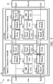
- the host optical transceiver module OTMH includes an optical detection unit 311, a conversion module 321, an electrical signal transmitter 331, an optical signal transmitter 341, a driving module 351, an idle detection unit 361, a photoelectric diode 371, and a control unit 381.
- the host optical transceiver module OTMH is coupled to the host 10 by the electrical signal transmission terminal ETx1 and the electrical signal receiving terminal ERx1, and is coupled to the optical fibers 531 and 532 by the optical signal transmission terminal OTx1 and the optical signal receiving terminal ORx1, respectively.
- the photoelectric diode 371 is coupled to the device optical transceiver module OTMD by the optical signal receiving terminal ORx1.
- the optical detection unit 311 is coupled between the photoelectric diode 371 and the control unit 381.
- the electrical signal transmitter 331 is coupled to the host 10 by the electrical signal transmission terminal ETx1.
- the conversion module 321 is coupled between the photoelectric diode 371 and the electrical signal transmitter 331.
- the optical signal transmitter 341 is coupled to the device optical transceiver module OTMD by the optical signal transmission terminal OTx1.
- the idle detection unit 361 and the driving module 351 are coupled to the host 10 by the electrical signal receiving terminal ERx1.
- the optical signal transmitter 341 is coupled between the driving module 351 and the optical signal transmission terminal OTx1.
- the idle detection unit 361 is coupled between the electrical signal receiving terminal ERx1 and the control unit 381.
- the control unit 381 is further coupled to the conversion module 321, the driving module 351, and the electrical signal transmitter 331.
- the control unit 381 controls the conversion module 321, the driving module 351, and the electrical signal transmitter 331 according to the detected signals from the optical signal detection unit 311 and the idle detection unit 361.
- the device optical transceiver module OTMD includes an optical signal detection unit 312, a conversion module 322, an electrical signal transmitter 332, an optical signal transmitter 342, a driving module 352, an idle detection unit 362, a photoelectric diode 372, and a control unit 382.
- the device optical transceiver module OTMD is coupled to the device 20 by the electrical signal transmission terminal ETx2 and the electrical signal receiving terminal ERx2, and is coupled to the optical fibers 531 and 532 by optical signal receiving terminal ORx2 and the optical signal transmission terminal OTx2, respectively.
- the photoelectric diode 372 is coupled to the host optical transceiver module OTMH by the optical signal receiving terminal ORx2.
- the optical detection unit 312 is coupled between the photoelectric diode 372 and the control unit 382.
- the electrical signal transmitter 332 is coupled to the device 20 by the electrical signal transmission terminal ETx2.
- the conversion module 322 is coupled between the photoelectric diode 372 and the electrical signal transmitter 332.
- the optical signal transmitter 342 is coupled to the host optical transceiver module OTMH by the optical signal transmission terminal OTx2.
- the idle detection unit 362 and the driving module 352 are coupled to the device 20 by the electrical signal receiving terminal ERx2.
- the optical signal transmitter 342 is coupled between the driving module 352 and the optical signal transmission terminal OTx2.
- the idle detection unit 362 is coupled between the electrical signal receiving terminal ERx2 and the control unit 382.
- the control unit 382 is further coupled to the conversion module 322, the driving module 352, and the electrical signal transmitter 332.
- the control unit 382 controls the conversion module 322, the driving module 352, and the electrical signal transmitter 332 according to the detected signals from the optical signal detection unit 312 and the idle detection unit 362.
- the optical signal detection units 311 and 312 are similar to the optical signal detection unit 310 in FIG. 2 .
- the conversion modules 321 and 322 are similar to the conversion module 320 in FIG. 2 .
- the electrical signal transmitters 331 and 332 are similar to the electrical signal transmitter 330 in FIG. 2 .
- the optical signal transmitters 341 and 342 are similar to the optical signal transmitter 340 in FIG. 2 .
- the conversion units 351 and 352 are similar to the conversion unit 350 in FIG. 2 .
- the idle detection units 361 and 362 are similar to the idle detection unit 360 in FIG. 2 .
- the photoelectric diode 371 and 372 are similar to the photoelectric diode 370 in FIG. 2 .
- the control units 381 and 382 are similar to the control unit 380 in FIG. 2 .
- the detailed descriptions of the same elements can be referred to in the earlier descriptions and will not be described again here.
- the host optical transceiver module OTMH and the device optical transceiver module OTMD can be regarded as the optical transceiver modules 31 and 32 in FIG. 1 .
- the optical signal transmission terminal OTx1, the optical signal receiving terminal ORx1, the electrical signal transmission terminal ETx1, and the electrical signal receiving terminal ERx1 in the host optical transceiver module OTMH can be regarded as the host optical transmission terminal, the host optical receiving terminal, the host electrical transmission terminal, and the host electrical receiving terminal.
- the optical signal transmission terminal OTx2, the optical signal receiving terminal ORx2, the electrical signal transmission terminal ETx2, and the electrical signal receiving terminal ERx2 in the device optical transceiver module OTMD can be regarded as the device optical transmission terminal, the device optical receiving terminal, the device electrical transmission terminal, and the device electrical receiving terminal.
- the link state U0 is a super speed connection effective state.
- the device transmits signals in the link state U0.
- the link states U1, U2, and U3 are power saving states, or low power link states.
- D_SM is a device state machine signal for representing the link state which the device 20 is operating in.
- D_Tx is a device transmission terminal signal for representing the transmission signal of the transmission terminal TxD in the device 20.
- device 20 transmits data of 5GT/s which is composed by a series of logic 1 and logic 0 via the transmission terminal TxD.
- device 20 transmits a signal every predetermined period (ex: 200ms) via the transmission terminal TxD.
- device 20 continues to transmit a common mode signal EIDLE representing that the device 20 is in idle state via the transmission terminal TxD.
- D_EIDLEDET is an idle detection signal of the device. The idle detection signal D_EIDLEDET of the device is logic 1 when the device 20 is idle.
- D_PD_OTx is a turn-off signal of the device optical transmission terminal. Power of the driving device 352 is turned off when the turn-off signal D_PD_OTx of the device optical transmission terminal is logic 1. Power of the driving device 352 is turned on when the turn-off signal D_PD_OTx of the device optical transmission terminal is logic 0.
- H_LOSDET is a detection signal of the host optical receiving terminal.
- the detection signal H_LOSDET of the host optical receiving terminal is logic 1 when the optical signal detection 311 detects that no optical signal is received via the host optical receiving terminal (ORx1).
- the detection signal H_LOSDET of the host optical receiving terminal is logic 0 when the optical signal detection unit 311 detects that an optical signal is received via the host optical receiving terminal (ORx1).
- H_PD_ORx is a turn-off signal of the host optical receiving terminal. Power of the conversion module 321 is turned off when the turn off signal H_PD_ORx of the host optical receiving terminal is logic 1. Power of the conversion module 321 is turned on when the turn off signal H_PD_ORx of the host optical receiving terminal is logic 0.
- H_EIDLEDET is a host idle detection signal.
- the host 10 is idle when the host idle detection signal H_EIDLEDET is logic 1.
- H_ORxR is a register signal of a host optical receiving terminal, and the register signal represents data stored in a register in the host optical transceiver module OTMH. Data stored in the register in the host optical transceiver module OTMH is reset to logic 0 when the host idle detection signal H_EIDLEDET changes from logic 1 to logic 0. Data stored in the register in the host optical transceiver module OTMH is set to logic 1 when the turn-off signal H_PD_ORx of the host optical receiving terminal is logic 1.
- H_PD_OTx is a turn-off signal of the host optical transmission terminal.
- Power of the driving module 351 is turned off when the turn-off signal H_PD_OTx of the host optical transmission terminal is logic 1. Power of the driving module 351 is turned on when the turn-off signal H_PD_OTx of the host optical transmission terminal is logic 0.
- D_LOSDET is a detection signal of the device optical receiving terminal. The detection signal D_LOSDET of the device optical receiving terminal is logic 1 when the optical signal detection unit 312 detects that no optical signal is received via the device optical receiving terminal (ORx2). The detection signal D_LOSDET of the device optical receiving terminal is logic 0 when the optical signal detection unit 312 detects that an optical signal is received via the device optical receiving terminal (ORx2).
- D_PD_ORx is a turn-off signal of the device optical receiving terminal. Power of the conversion module 322 is turned off when the turn-off signal D_PD_ORx of the device optical receiving terminal is logic 1. Power of the conversion module 322 is turned on when the turn-off signal D_PD_ORx of the device optical receiving terminal is logic 0.
- FIG. 6 is a signal timing diagram of the optical transmission system 5 when the device 20 operates in the link state U2 or U3 according to an embodiment of the present invention.
- the transmission terminal TxD transmits the common mode signal EIDLE such that the idle detection unit 362 detects that the device 20 is in the idle state when the device 20 operates in the link state U2 or U3.
- the control unit 382 turns on and off the power of the driving module 352 periodically. Namely, the optical signal is transmitted periodically via the device optical transmission terminal (OTx2).
- t_OTxOFF is a period during which power to the driving module 352 is turned off (i.e., a period during which no optical signal is transmitted via the device optical transmission terminal).
- t_OTxON is a period during which power to the driving module 352 is turned on (i.e., a period during which an optical signal is transmitted via the device optical transmission terminal).
- FIG. 7 is a signal timing diagram of the optical transmission system 5 when the device 20 operates in the link state U1 according to an embodiment of the present invention.
- the device 20 transmits a signal D_Tx every specific period (such as t_Ping) via the transmission terminal TxD when the device 20 operates in the link state U1.
- Power of the driving module 352 can be maintained at turn-on (i.e., D_PD_OTx is logic 0) in the link state U1 by setting the period t_EDILE to be larger than the specific period t_Ping.
- FIG. 8 is a signal timing diagram of the optical transmission system 5 when device 20 operates in the link state U2 or U3 according to an embodiment of the present invention.
- the device 20 transmits the common mode signal EIDLE via the transmission terminal TxD such that the idle detection unit 362 detects that the device 20 is idle.
- the upper part of FIG. 8 is same as that shown in FIG. 6 .
- the detailed descriptions of the same elements can be referred to in the earlier descriptions and will not be described again here.
- the following embodiment is illustrated according to the lower part of FIG. 8 .
- t_OTxOFF is a period that power of the driving module 351 is turned off (i.e., a period that no optical signal is transmitted via the host optical transmission terminal).
- t_OTxON is a period that power of the driving module 351 is turned on (i.e., a period that an optical signal is transmitted via the host optical transmission terminal).
- link state U1 host 10 does not transmit the signal every specific period like the device 20 does, so that the host optical transceiver module OTMH cannot distinguish the link states U1, U2, and U3 based solely on whether the host 10 is idle for the period t_EIDLE.
- the host optical transceiver module OTMH can determine whether the device 20 operates in the link state U2 or U3 indirectly based on whether no optical signal is received via the host optical receiving terminal (ORx1) for the period t_ORxLOS. Whether no optical signal is received via the host optical receiving terminal (ORx1) for the period t_ORxLOS can be recorded by setting the register in the host optical transceiver module OTMH.
- the power of the driving module 351 is turned on and off periodically when the host 10 is idle for the period t_EIDLE and no optical signal is received via the host optical receiving terminal (ORx1) for the period t_ORxLOS.
- the power of the driving module 351 is turned on and off periodically when the host 10 is idle for the period t_EIDLE and the data of the register is set from a first logic level to a second logic level.
- the period t_EIDLE of the host optical transceiver module OTMH can be less than 100ms or can be about 1ms.
- the optical transmission devices of the present invention can perform corresponding power management operations for power saving based on the power management of the connected electronic device.
- USB 3.0 a person having ordinary skill in the art can apply the host and the device in USB 3.1 or USB 3 series based on the optical transceiver module, the optical transmission device, and the optical transmission method as recited in the present specification.
Landscapes
- Physics & Mathematics (AREA)
- Electromagnetism (AREA)
- Engineering & Computer Science (AREA)
- Computer Networks & Wireless Communication (AREA)
- Signal Processing (AREA)
- Optical Communication System (AREA)
Description
- The present invention relates to an optical transmission device, and in particular to an optical transmission device applied to universal serial bus.
- With the development of the optical transmission field, the optical fiber transmission has a developed superiority in terms of transmission speed, transmission distance, and the anti-interference ability. As a result, the optical transmission devices are now being applied more widely. Due to the superiority of the optical transmission field, there is more and more demand for connecting a host and a device to an optical transmission device, such that hosts and devices with traditional interfaces (such as a peripheral component interconnect express interface or a universal serial bus 3.0 interface) can perform optical fiber communication using the optical transmission device. In the optical transmission devices, the active optical cable (AOC) includes two electrical-to-optical/optical-to-electrical chips located on the host terminal and the device terminal. The host and the device can perform optical fiber communication through the active optical fiber without changing the hardware. The conventional active optical cable does not include a power management function. As a result, even when the USB link components enter a low power-consumption state, the chips using active optical cables can still operate in a high power-consumption state, causing unnecessary power consumption. Therefore, a new active optical cable and an optical transmission method are needed to solve such problems.
- Some active optical cables with power management functions have been proposed.
- For example, U.S. Patent Application Publication No.
US 2012/0191997 A1 discloses an active optical cable that incorporates a power management solution. The active optical cable has plugs that are configured to mate with respective USB sockets. The active optical cable is used to interconnect a USB host with a USB device. To the USB host and to the USB device, the active optical cable appears to be a standard USB electrical cable. Each of the plugs of the active optical cable has an optical-to-electrical and an electrical-to-optical conversion module that converts electrical USB signals output from the USB host or USB device into optical signals and converts optical signals carried on the optical fibers of the active optical cable into electrical signals. The plugs include controllers that monitor certain conditions of the active optical cable and that select the power levels to be used in the plugs based on detected conditions. - Further, U.S. Patent Application Publication No.
US 2013/0129359 A1 describes a data transport system for transporting data and auxiliary signals over an optical link comprising a transmitter, a receiver and an optical link. The transmitter and receiver are coupled to a first end of the optical link. The optical link includes a number of optical channels. A controller is coupled to the transmitter and the receiver, and controls the transmitter and the receiver to operate in a first state when data are detected at the input of the transmitter. Data are transported via the data transport system in the first state. The controller controls the transmitter and the receiver to also operate in a second state when the data are detected as absent at the input of the transmitter. Data are prevented from being transported via the data transport system in the second state. - The invention is defined in
claims - According to a first aspect of the invention, an optical transmission device is provided. The optical transmission device is coupled between a first electronic device and a second electronic device, and includes a first optical transceiver module coupled to the first electronic device; a second optical transceiver module coupled to the second electronic device; and first and second optical fibers coupled between the first optical transceiver module and the second optical transceiver module. The second optical transceiver module periodically transmits an optical signal to the first optical transceiver module when the second electronic device is idle for a first predetermined period.
- According to a second aspect of the invention, an optical transceiver module is provided. The optical transceiver module includes an optical-to-electrical transformation path with an electrical signal transmitter; a conversion module driving the electrical signal transmitter to transmit an electrical signal via an electrical signal transmission terminal according to an optical signal received in the optical-to-electrical transformation path; and a control unit turning off power of the conversion module when no optical signal is received in the optical-to-electrical transformation path for a first predetermined period.
- According to a third aspect of the invention, a further optical transceiver module is provided. The optical transceiver module includes an electrical-to-optical transform path with an optical signal transmitter; a driving module driving the optical signal transmitter to transmit an optical signal via an optical signal transmission terminal according to an electrical signal received in the electrical-to-optical transformation path; and an idle signal detection unit, outputting an idle detection signal to a control unit according to an idle signal received in the electrical-to-optical transformation path.
- According to a fourth aspect of the invention, a still further optical transceiver module is provided. The optical transceiver module has an optical receiving terminal, an optical transmission terminal, an electrical signal receiving terminal, and an electrical signal transmission terminal. The optical transceiver module further includes an optical detection unit coupled to the optical receiving terminal; an electrical signal transmitter coupled to the electrical signal transmission terminal; a conversion module coupled between the optical receiving terminal and the electrical signal transmitter; an optical signal transmitter coupled to the optical signal transmission terminal; a driving module coupled between the electrical signal receiving terminal and the optical signal transmitter; an idle detection unit coupled to the electrical signal receiving terminal; and a control unit coupled to the optical detection unit, the conversion module, the driving module, and the idle detection unit.
- A detailed description is given in the following embodiments with reference to the accompanying drawings.
- The present invention can be more fully understood by reading the subsequent detailed description and examples with references made to the accompanying drawings, wherein:
-
FIG. 1 is a schematic diagram of an optical transmission system according to an embodiment of the present invention; -
FIG. 2 is a schematic diagram of an optical transceiver module according to an embodiment of the present invention; -
FIG. 3 is a signal timing diagram of the optical transceiver module according to an embodiment of the present invention; -
FIG. 4 is a signal timing diagram of the optical transceiver module according to an embodiment of the present invention; -
FIG. 5 is a schematic diagram of an optical transmission system according to an embodiment of the present invention; -
FIG. 6 is a signal timing diagram of the optical transmission system when the device operates in the link state U2 or U3 according to an embodiment of the present invention; -
FIG. 7 is a signal timing diagram of the optical transmission system when the device operates in the link state U1 according to an embodiment of the present invention; and -
FIG. 8 is a signal timing diagram of the optical transmission system when the device operates in the link state U2 or U3 according to an embodiment of the present invention. - The following description is of the best-contemplated operation of carrying out the invention. This description is made for the purpose of illustrating the general principles of the invention and should not be taken in a limiting sense. Certain terms and figures are used throughout the description and following claims to refer to particular components. As one skilled in the art will appreciate, manufacturers may refer to a component by different names. This document does not intend to distinguish between components that differ in name but not function. The terms "component", "system" and "device" used in the present invention could be the entity relating to the computer which is hardware, software, or a combination of hardware and software. In the following description and in the claims, the terms "include" and "comprise" are used in an open-ended fashion, and thus should be interpreted to mean "include, but not limited to ...". Also, the term "couple" is intended to mean either an indirect or direct electrical connection. Accordingly, if one device is coupled to another device, that connection may be through a direct electrical connection, or through an indirect electrical connection via other devices and connections.
-
FIG. 1 is a schematic diagram of anoptical transmission system 1 according to an embodiment of the present invention. Theoptical transmission system 1 includes ahost 10, adevice 20, and anoptical transmission device 30 connected between thehost 10 and thedevice 20. Thehost 10 may be a high-speed electronic transceiver device having a PCIE interface or a USB3.0 interface or supporting hot-plugging function, and includes a transmission terminal TxH and a receiving terminal RxH. Thedevice 20 can be a high-speed electronic connection device having a PCIE interface or a USB3.0 interface or supporting hot-plugging function, and includes a transmission terminal TxD and a receiving terminal RxD. Theoptical transmission device 30 can be an active optical cable, performing the electrical-to-optical/optical-to-electrical transformation and optical fiber communication between thehost 10 and thedevice 20. - The
optical transmission device 30 includes anoptical transceiver module 31 coupled to thehost 10 and anoptical transceiver module 32 coupled to thedevice 20. Theoptical transmission device 30 further includesoptical fibers optical transceiver modules optical transceiver module 31 includes an electrical signal transmission terminal ETx1 and an electrical signal receiving terminal ERx1 for transmitting and receiving an electrical signal. Theoptical transceiver module 31 further includes an optical signal transmission terminal OTx1 and an optical signal receiving terminal ORx1 for transmitting and receiving an optical signal. Theoptical transceiver module 32 includes an electrical signal transmission terminal ETx2 and an electrical signal receiving terminal ERx2 for transmitting and receiving an electrical signal. Theoptical transceiver module 32 further includes an optical signal transmission terminal OTx2 and an optical signal receiving terminal ORx2 for transmitting and receiving an optical signal. The electrical signal receiving terminal ERx1 in theoptical transceiver module 31 is coupled to the transmission terminal TxH of thehost 10 by a cable for receiving the electrical signal transmitted by thehost 10. Theoptical transceiver module 31 performs an electrical-to-optical transformation on the electrical signal received by electrical signal receiving terminal ERx1 to obtain an optical signal, and transmits the obtained optical signal from the optical signal transmission terminal OTx1 to the optical signal receiving terminal ORx2 by theoptical fiber 331. Theoptical transceiver module 32 performs an optical-to-electrical transformation on the optical signal received by the optical signal receiving terminal ORx2 to obtain an electrical signal, and transmits the obtained electrical signal from the electrical signal transmission terminal ETx2 to the receiving terminal RxD of thedevice 20 by the cable. The electrical signal receiving terminal ERx2 is coupled to the transmission terminal TxD of thedevice 20 by the cable to receive the electrical signal transmitted by thedevice 20. Theoptical transceiver module 32 performs an electrical-to-optical transformation on the electrical signal received by the electrical signal receiving terminal ERx2 to obtain an optical signal, and transmits the obtained optical signal from optical signal transmission terminal OTx2 to optical signal receiving terminal ORx1 by theoptical fiber 332. Theoptical transceiver module 31 performs an optical-to-electrical transformation on the optical signal received by the optical signal receiving terminal ORx1 to obtain an electrical signal, and transmits the obtained electrical signal from an electrical signal transmission terminal ETx1 to a receiving terminal RxH of thehost 10 by the cable. -
FIG. 2 is a schematic diagram of an optical transceiver module OTM according to an embodiment of the present invention. As shown inFIG. 2 , aphotoelectric diode 370 is coupled to an optical signal receiving terminal ORx, and anelectrical signal transmitter 330 is coupled to the electrical signal transmission terminal ETx, and aconversion module 320 is coupled between thephotoelectric diode 370 and theelectrical signal transmitter 330. Anoptical signal transmitter 340 is coupled between an optical signal transmission terminal OTx and adriving module 350. Thedriving module 350 is coupled between theoptical signal transmitter 340 and an electrical signal receiving terminal ERx. An opticalsignal detection unit 310 is coupled between thephotoelectric diode 370 and acontrol unit 380. Anidle detection unit 360 is coupled between an electrical signal receiving terminal ERx and thecontrol unit 380. Thecontrol unit 380 is further coupled to theconversion module 320, thedriving module 350, and theelectrical signal transmitter 330. Thecontrol unit 380 controls theconversion module 320, thedriving module 350, and theelectrical signal transmitter 330 according to detection signals of the opticalsignal detection unit 310 and theidle detection unit 360. The optical transceiver module OTM is coupled to an electronic device (not shown in figure) by the electrical signal transmission terminal ETx and the electrical signal receiving terminal ERx. The optical transceiver module OTM can be theoptical transceiver module 31 or theoptical transceiver module 32 shown inFIG. 1 . The optical transceiver module OTM has an electrical-to-optical transformation path for transforming an electrical signal to an optical signal. The electrical-to-optical transformation path includes thedriving module 350 and theoptical signal transmitter 340 at least. According to the received electrical signal, thedriving module 350 draws a current and theoptical signal transmitter 340 is driven to perform the optical signal transmission based on the current drawn by thedriving module 350. In one embodiment, theoptical signal transmitter 340 can be a vertical-cavity surface-emitting laser. The optical transceiver module OTM further has thecontrol unit 380 and theidle detection unit 360. Theidle detection unit 360 is coupled between the electrical signal receiving terminal ERx and thecontrol unit 380. In the electrical-to-optical transformation path, theidle detection unit 360 detects whether the electrical device is idle according to the received signal received by the electrical signal receiving terminal ERx. Thecontrol unit 380 turns on and off power of thedriving module 350 periodically when the electrical device is idle for a first predetermined period. Correspondingly, theoptical signal transmitter 340 also transmits the optical signal periodically to save power. - The optical transceiver module OTM also has an optical-to-electrical transformation path for transforming an optical signal to an electrical signal. The optical-to-electrical transformation path at least includes the
photoelectric diode 370, theconversion module 320, and theelectrical signal transmitter 330. Thephotoelectric diode 370 transforms the received optical signal to a current, and theconversion module 320 transforms the current to a voltage, and theelectrical signal transmitter 330 pre-drives the voltage and then performs transmission of the pre-driven voltage. In one embodiment, theelectrical signal transmitter 330 also has a buffer function. The optical transceiver module OTM also has the opticalsignal detection unit 310. The opticalsignal detection unit 310 is coupled between thephotoelectric diode 370 and thecontrol unit 380. In the optical-to-electrical transformation path, the opticalsignal detection unit 310 detects the current output from thephotoelectric diode 370 to determine whether the optical signal is received, and thecontrol unit 380 turns off power of theconversion module 320 when the opticalsignal detection unit 310 does not receive any optical signal for a second predetermined period. Correspondingly, theelectrical signal transmitter 330 also stops transmitting the electrical signal for power saving. In one embodiment, the power of theelectrical signal transmitter 330 can also be turned off by thecontrol unit 380. - In one embodiment, an electrical signal transmission terminal ETx is coupled to a receiving terminal of the electronic device, and an electrical signal receiving terminal ERx is coupled to a transmission terminal of the electronic device. The optical transceiver module OTM has corresponding operations in response to the power management of the electronic device. The electronic device transmits a corresponding electrical idle signal to the electrical signal receiving terminal ERx when the electronic device enters the low power-consumption state and is idle. The following embodiment is illustrated by taking
FIG. 3 for example.FIG. 3 is a signal timing diagram of the optical transceiver module OTM according to an embodiment of the present invention. InFIG. 3 , EIDLEDET is an idle detection signal which represents theidle detection unit 360 detects that the coupled electronic device enters an idle state. The idle detection signal EIDLEDET islogic 1 when the coupled electronic device is idle. InFIG. 3 , PD_OTx represents a turn-off signal of the optical signal transmission terminal that is transmitted by thecontrol unit 380. When the turn-off signal PD_OTx of the optical signal transmission terminal islogic 1, power of thedriving module 350 is turned off. Namely, thedriving module 350 stops drawing the current from the received electrical signal received by the electrical signal receiving terminal ERx, and thus, theoptical signal transmitter 340 stops transmitting the optical signal to the optical signal transmission terminal OTx. When the turn-off signal PD_OTx of the optical signal transmission terminal is logic 0, power of thedriving module 350 is turned on. Namely, thedriving module 350 draws the current from the received electrical signal received by the electrical signal receiving terminal ERx, and drives theoptical signal transmitter 340 to transmit the optical signal by the optical signal transmission terminal OTx. As shown inFIG. 3 , thecontrol unit 380 turns on and off the power of thedriving module 350 periodically when the electronic device is idle for a period t_EIDLE. As a result, theoptical signal transmitter 340 also transmits the optical signal periodically. The turn-off period of thedriving module 350 is t_OTxOFF, and the turn-on period of thedriving module 350 is t_OTxON. Once the electronic device is no longer idle (i.e., the idle detection signal EIDLEDET is logic 0), thecontrol unit 380 turns on the power of the driving module 350 (i.e., the turn-off signal PD_OTx of the optical signal transmission terminal is logic 0) accordingly. In one embodiment, if the optical signal receiving terminal of another optical transceiver module (not shown) coupled to the optical transceiver module OTM does not receive any optical signal for a predetermined unplugging period, the other optical transceiver module determines that the electronic device is already unplugged. As a result, the turn-off period t_OTxOFF of thedriving module 350 must be less than the predetermined unplugging period to avoid misjudging that the electronic device is unplugged, even when it is actually idle. In the present specification, the optical signal transmitter can be a vertical-cavity surface-emitting laser. - The following embodiment is illustrated in
FIG. 4. FIG. 4 is a signal timing diagram of the optical transceiver module OTM according to an embodiment of the present invention. InFIG. 4 , LOSDET represents a detection signal of the optical signal which is transmitted by the opticalsignal detection unit 310. The detection signal LOSDET of the optical signal islogic 1 when the opticalsignal detection unit 310 determines that the optical signal receiving terminal ORx does not receive any optical signals. The detection signal LOSDET of the optical signal is logic 0 when the optical signal receiving terminal ORx receives optical signals. InFIG. 4 , PD_ORx represents a turn-off signal of the optical signal receiving terminal that is transmitted by thecontrol unit 380. When the turn-off signal PD_ORx of the optical signal receiving terminal islogic 1, the power of theconversion module 320 is turned off. Namely, theconversion module 320 stops converting the current to the voltage. As a result, theelectrical signal transmitter 330 stops transmitting the electrical signal to the electrical signal transmission terminal ETx. In one embodiment, the power of theelectrical signal transmitter 330 can be further turned off. When the turn-off signal PD_ORx of the optical signal receiving terminal is logic 0, the power of theconversion module 320 is turned on. Namely, theconversion module 320 converts the current to the voltage, and drives theelectrical signal transmitter 330 to transmit the electrical signal via the electrical signal transmission terminal ETx. As shown inFIG. 4 , when the opticalsignal detection unit 310 determines that no optical signal is received for the period t_ORxLOS, thecontrol unit 380 turns off the power of theconversion module 320, such that the electrical signal stops transmitting via the electrical signal transmission terminal ETx. Once the opticalsignal detection unit 310 receives the optical signal (i.e., the detection signal LOSDET of the optical signal is logic 0), thecontrol unit 380 turns on the power of the conversion module 320 (i.e., the turn-off signal PD_ORx of the optical signal receiving terminal is logic 0). -
FIG. 5 is a schematic diagram of anoptical transmission system 5 according to an embodiment of the present invention. Theoptical transmission system 5 includes ahost 10, adevice 20, and anoptical transmission device 50 connected between thehost 10 and thedevice 20. Thehost 10 and thedevice 20 are similar to those shown inFIG. 1 . The detailed descriptions of the same elements can be referred to in the earlier descriptions and will not be described again here. Theoptical transmission device 50 includes a host optical transceiver module OTMH coupled to thehost 10 and a device optical transceiver module OTMD coupled to thedevice 20. Theoptical transmission device 50 further includesoptical fibers optical detection unit 311, aconversion module 321, anelectrical signal transmitter 331, anoptical signal transmitter 341, adriving module 351, anidle detection unit 361, aphotoelectric diode 371, and acontrol unit 381. The host optical transceiver module OTMH is coupled to thehost 10 by the electrical signal transmission terminal ETx1 and the electrical signal receiving terminal ERx1, and is coupled to theoptical fibers photoelectric diode 371 is coupled to the device optical transceiver module OTMD by the optical signal receiving terminal ORx1. Theoptical detection unit 311 is coupled between thephotoelectric diode 371 and thecontrol unit 381. Theelectrical signal transmitter 331 is coupled to thehost 10 by the electrical signal transmission terminal ETx1. Theconversion module 321 is coupled between thephotoelectric diode 371 and theelectrical signal transmitter 331. Theoptical signal transmitter 341 is coupled to the device optical transceiver module OTMD by the optical signal transmission terminal OTx1. Theidle detection unit 361 and thedriving module 351 are coupled to thehost 10 by the electrical signal receiving terminal ERx1. Theoptical signal transmitter 341 is coupled between the drivingmodule 351 and the optical signal transmission terminal OTx1. Theidle detection unit 361 is coupled between the electrical signal receiving terminal ERx1 and thecontrol unit 381. Thecontrol unit 381 is further coupled to theconversion module 321, thedriving module 351, and theelectrical signal transmitter 331. Thecontrol unit 381 controls theconversion module 321, thedriving module 351, and theelectrical signal transmitter 331 according to the detected signals from the opticalsignal detection unit 311 and theidle detection unit 361. - The device optical transceiver module OTMD includes an optical
signal detection unit 312, aconversion module 322, anelectrical signal transmitter 332, anoptical signal transmitter 342, adriving module 352, anidle detection unit 362, aphotoelectric diode 372, and acontrol unit 382. The device optical transceiver module OTMD is coupled to thedevice 20 by the electrical signal transmission terminal ETx2 and the electrical signal receiving terminal ERx2, and is coupled to theoptical fibers photoelectric diode 372 is coupled to the host optical transceiver module OTMH by the optical signal receiving terminal ORx2. Theoptical detection unit 312 is coupled between thephotoelectric diode 372 and thecontrol unit 382. Theelectrical signal transmitter 332 is coupled to thedevice 20 by the electrical signal transmission terminal ETx2. Theconversion module 322 is coupled between thephotoelectric diode 372 and theelectrical signal transmitter 332. Theoptical signal transmitter 342 is coupled to the host optical transceiver module OTMH by the optical signal transmission terminal OTx2. Theidle detection unit 362 and thedriving module 352 are coupled to thedevice 20 by the electrical signal receiving terminal ERx2. Theoptical signal transmitter 342 is coupled between the drivingmodule 352 and the optical signal transmission terminal OTx2. Theidle detection unit 362 is coupled between the electrical signal receiving terminal ERx2 and thecontrol unit 382. Thecontrol unit 382 is further coupled to theconversion module 322, thedriving module 352, and theelectrical signal transmitter 332. Thecontrol unit 382 controls theconversion module 322, thedriving module 352, and theelectrical signal transmitter 332 according to the detected signals from the opticalsignal detection unit 312 and theidle detection unit 362. The opticalsignal detection units signal detection unit 310 inFIG. 2 . Theconversion modules conversion module 320 inFIG. 2 . Theelectrical signal transmitters electrical signal transmitter 330 inFIG. 2 . Theoptical signal transmitters optical signal transmitter 340 inFIG. 2 . Theconversion units conversion unit 350 inFIG. 2 . Theidle detection units idle detection unit 360 inFIG. 2 . Thephotoelectric diode photoelectric diode 370 inFIG. 2 . Thecontrol units control unit 380 inFIG. 2 . The detailed descriptions of the same elements can be referred to in the earlier descriptions and will not be described again here. In some embodiments, the host optical transceiver module OTMH and the device optical transceiver module OTMD can be regarded as theoptical transceiver modules FIG. 1 . As a result, the optical signal transmission terminal OTx1, the optical signal receiving terminal ORx1, the electrical signal transmission terminal ETx1, and the electrical signal receiving terminal ERx1 in the host optical transceiver module OTMH can be regarded as the host optical transmission terminal, the host optical receiving terminal, the host electrical transmission terminal, and the host electrical receiving terminal. On the other hand, the optical signal transmission terminal OTx2, the optical signal receiving terminal ORx2, the electrical signal transmission terminal ETx2, and the electrical signal receiving terminal ERx2 in the device optical transceiver module OTMD can be regarded as the device optical transmission terminal, the device optical receiving terminal, the device electrical transmission terminal, and the device electrical receiving terminal. - According to the definition of the USB 3.0 specification, there are four link states U0, U1, U2, and U3. The link state U0 is a super speed connection effective state. The device transmits signals in the link state U0. The link states U1, U2, and U3 are power saving states, or low power link states. In the following description, D_SM is a device state machine signal for representing the link state which the
device 20 is operating in. D_Tx is a device transmission terminal signal for representing the transmission signal of the transmission terminal TxD in thedevice 20. In the link state U0,device 20 transmits data of 5GT/s which is composed by a series oflogic 1 and logic 0 via the transmission terminal TxD. In the link state U1,device 20 transmits a signal every predetermined period (ex: 200ms) via the transmission terminal TxD. In the link states U2 and U3,device 20 continues to transmit a common mode signal EIDLE representing that thedevice 20 is in idle state via the transmission terminal TxD. D_EIDLEDET is an idle detection signal of the device. The idle detection signal D_EIDLEDET of the device islogic 1 when thedevice 20 is idle. D_PD_OTx is a turn-off signal of the device optical transmission terminal. Power of thedriving device 352 is turned off when the turn-off signal D_PD_OTx of the device optical transmission terminal islogic 1. Power of thedriving device 352 is turned on when the turn-off signal D_PD_OTx of the device optical transmission terminal is logic 0. H_LOSDET is a detection signal of the host optical receiving terminal. The detection signal H_LOSDET of the host optical receiving terminal islogic 1 when theoptical signal detection 311 detects that no optical signal is received via the host optical receiving terminal (ORx1). The detection signal H_LOSDET of the host optical receiving terminal is logic 0 when the opticalsignal detection unit 311 detects that an optical signal is received via the host optical receiving terminal (ORx1). H_PD_ORx is a turn-off signal of the host optical receiving terminal. Power of theconversion module 321 is turned off when the turn off signal H_PD_ORx of the host optical receiving terminal islogic 1. Power of theconversion module 321 is turned on when the turn off signal H_PD_ORx of the host optical receiving terminal is logic 0. - H_EIDLEDET is a host idle detection signal. The
host 10 is idle when the host idle detection signal H_EIDLEDET islogic 1. H_ORxR is a register signal of a host optical receiving terminal, and the register signal represents data stored in a register in the host optical transceiver module OTMH. Data stored in the register in the host optical transceiver module OTMH is reset to logic 0 when the host idle detection signal H_EIDLEDET changes fromlogic 1 to logic 0. Data stored in the register in the host optical transceiver module OTMH is set tologic 1 when the turn-off signal H_PD_ORx of the host optical receiving terminal islogic 1. H_PD_OTx is a turn-off signal of the host optical transmission terminal. Power of thedriving module 351 is turned off when the turn-off signal H_PD_OTx of the host optical transmission terminal islogic 1. Power of thedriving module 351 is turned on when the turn-off signal H_PD_OTx of the host optical transmission terminal is logic 0. D_LOSDET is a detection signal of the device optical receiving terminal. The detection signal D_LOSDET of the device optical receiving terminal islogic 1 when the opticalsignal detection unit 312 detects that no optical signal is received via the device optical receiving terminal (ORx2). The detection signal D_LOSDET of the device optical receiving terminal is logic 0 when the opticalsignal detection unit 312 detects that an optical signal is received via the device optical receiving terminal (ORx2). D_PD_ORx is a turn-off signal of the device optical receiving terminal. Power of theconversion module 322 is turned off when the turn-off signal D_PD_ORx of the device optical receiving terminal islogic 1. Power of theconversion module 322 is turned on when the turn-off signal D_PD_ORx of the device optical receiving terminal is logic 0. -
FIG. 6 is a signal timing diagram of theoptical transmission system 5 when thedevice 20 operates in the link state U2 or U3 according to an embodiment of the present invention. As shown inFIG. 6 , the transmission terminal TxD transmits the common mode signal EIDLE such that theidle detection unit 362 detects that thedevice 20 is in the idle state when thedevice 20 operates in the link state U2 or U3. When thedevice 20 is idle for a period t_EIDLE, thecontrol unit 382 turns on and off the power of thedriving module 352 periodically. Namely, the optical signal is transmitted periodically via the device optical transmission terminal (OTx2). t_OTxOFF is a period during which power to thedriving module 352 is turned off (i.e., a period during which no optical signal is transmitted via the device optical transmission terminal). t_OTxON is a period during which power to thedriving module 352 is turned on (i.e., a period during which an optical signal is transmitted via the device optical transmission terminal). Once thedevice 20 is no longer idle, thecontrol unit 382 turns on the power of thedriving module 352. When no optical signal is received via the host optical receiving terminal (ORx1) for the period t_ORxLOS, thecontrol unit 381 turns off the power of the conversion module 321 (i.e., H_PD_ORx is logic 1). Namely, the electrical signal is stopped transmitting via the host electrical transmission terminal (ETx1). Once the optical signal is received via the host optical receiving terminal (ORx1), thecontrol unit 381 turns on power of the conversion module 321 (i.e., H_PD_ORx is logic 0). -
FIG. 7 is a signal timing diagram of theoptical transmission system 5 when thedevice 20 operates in the link state U1 according to an embodiment of the present invention. As shown inFIG. 7 , thedevice 20 transmits a signal D_Tx every specific period (such as t_Ping) via the transmission terminal TxD when thedevice 20 operates in the link state U1. Power of thedriving module 352 can be maintained at turn-on (i.e., D_PD_OTx is logic 0) in the link state U1 by setting the period t_EDILE to be larger than the specific period t_Ping. -
FIG. 8 is a signal timing diagram of theoptical transmission system 5 whendevice 20 operates in the link state U2 or U3 according to an embodiment of the present invention. As shown inFIG. 8 , when thedevice 20 is in the link state U2 or U3, thedevice 20 transmits the common mode signal EIDLE via the transmission terminal TxD such that theidle detection unit 362 detects that thedevice 20 is idle. The upper part ofFIG. 8 is same as that shown inFIG. 6 . The detailed descriptions of the same elements can be referred to in the earlier descriptions and will not be described again here. The following embodiment is illustrated according to the lower part ofFIG. 8 . When thehost 10 is idle (i.e., H_EIDLEDET is logic 1) for the period t_EIDLE and no optical signal is received via the host optical receiving terminal (ORx1) for the period t_ORxLOS, power of thedriving module 351 is turned on and off periodically. Namely, the optical signal is transmitted periodically via the host terminal optical transmission terminal. t_OTxOFF is a period that power of thedriving module 351 is turned off (i.e., a period that no optical signal is transmitted via the host optical transmission terminal). t_OTxON is a period that power of thedriving module 351 is turned on (i.e., a period that an optical signal is transmitted via the host optical transmission terminal). Once thehost 10 is no longer idle, power of thedriving module 351 is turned on accordingly. In link state U1,host 10 does not transmit the signal every specific period like thedevice 20 does, so that the host optical transceiver module OTMH cannot distinguish the link states U1, U2, and U3 based solely on whether thehost 10 is idle for the period t_EIDLE. The host optical transceiver module OTMH can determine whether thedevice 20 operates in the link state U2 or U3 indirectly based on whether no optical signal is received via the host optical receiving terminal (ORx1) for the period t_ORxLOS. Whether no optical signal is received via the host optical receiving terminal (ORx1) for the period t_ORxLOS can be recorded by setting the register in the host optical transceiver module OTMH. As a result, unlike turning on and off the power of thedriving module 352 periodically based on a single condition (i.e., thedevice 20 is idle for the period t_EIDLE), the power of thedriving module 351 is turned on and off periodically when thehost 10 is idle for the period t_EIDLE and no optical signal is received via the host optical receiving terminal (ORx1) for the period t_ORxLOS. In one embodiment, the power of thedriving module 351 is turned on and off periodically when thehost 10 is idle for the period t_EIDLE and the data of the register is set from a first logic level to a second logic level. When no optical signal is received via the device optical receiving terminal (ORx2) for the period t_ORxLOS, power of theconversion module 322 is turned off (D_PD_ORx is logic 1). Namely, the electrical signal stops transmitting via the device electrical transmission terminal (ETx2). Once an optical signal is received via the device optical receiving terminal (ORx2), power of theconversion module 322 is turned on (D_PD_ORx is logic 0) accordingly. - In one embodiment, because the
host 10 performs receiver terminal detection every predetermined period (such as 100ms) in the link state U2 or U3, the period t_EIDLE of the host optical transceiver module OTMH can be less than 100ms or can be about 1ms. - As mentioned above, according to the above embodiments, the optical transmission devices of the present invention can perform corresponding power management operations for power saving based on the power management of the connected electronic device.
- Though the host and the device mentioned in the specification support USB 3.0, a person having ordinary skill in the art can apply the host and the device in USB 3.1 or USB 3 series based on the optical transceiver module, the optical transmission device, and the optical transmission method as recited in the present specification.
- Although embodiments of the present disclosure and their advantages have been described in detail, it should be understood that various changes, substitutions and alterations can be made herein without departing from the scope of the disclosure as defined by the appended claims. For example, it will be readily understood by those skilled in the art that many of the features, functions, processes, and materials described herein may be varied while remaining within the scope of the present disclosure. Moreover, the scope of the present application is not intended to be limited to the particular embodiments of the process, machine, manufacture, composition of matter, means, methods and steps described in the specification. As one of ordinary skill in the art will readily appreciate from the disclosure of the present disclosure, processes, machines, manufacture, compositions of matter, means, methods, or steps, presently existing or later to be developed, that perform substantially the same function or achieve substantially the same result as the corresponding embodiments described herein may be utilized according to the present disclosure. Accordingly, the appended claims are intended to include within their scope such processes, machines, manufacture, compositions of matter, means, methods, or steps. In addition, each claim constitutes a separate embodiment, and the combination of various claims and embodiments are within the scope of the disclosure.
Claims (15)
- An optical transceiver module, comprising:
an electrical-to-optical transformation path, comprising:an optical signal transmitter (340);a driving module (350) configured to drive the optical signal transmitter (340) to transmit an optical signal via an optical signal transmission terminal (OTx) according to an electrical signal received via an electrical signal receiving terminal (ERx); andan idle signal detection unit (360) configured to detect whether an electrical device (10, 20) is in idle mode according to the electrical signal received via the electrical signal receiving terminal (ERx) and to output an idle detection signal to a control unit (380) according to an idle signal received via the electrical signal receiving terminal (ERx) so that the idle detection signal represents when the electrical device (10, 20) is in idle mode;wherein the control unit (380) is configured to turn on and off power of the driving module (350) periodically while the idle mode is detected when the idle signal detection unit (360) detects that the idle signal is received via the electrical signal receiving terminal (ERx) for a first predetermined period. - The optical transceiver module of claim 1, further comprising:
an optical-to-electrical transformation path, comprising:an electrical signal transmitter (330);a photoelectric diode (370) configured to output a current according to an optical signal received via an optical signal receiving terminal (ORx); anda conversion module (320) configured to transform the current to a voltage for driving the electrical signal transmitter (330) and to drive the electrical signal transmitter (330) to transmit an electrical signal via an electrical signal transmission terminal (ETx) according to the optical signal received via the optical signal receiving terminal (ORx);wherein the control unit (380) is configured to turn off power of the conversion module (320) when no optical signal is received for a second predetermined period via the optical signal receiving terminal (ORx). - The optical transceiver module of claim 2, wherein the control unit (380) is further configured to turn off power of the electrical signal transmitter (330) when determining that no optical signal is received for the second predetermined period.
- The optical transceiver module of claim 2 or 3, further comprising an optical signal detection unit (310) configured to detect the current output from the photoelectric diode (370) to determine whether the optical signal is received.
- The optical transceiver module of claim 4, wherein the control unit (380) is configured to turn on and off power of the driving module (350) periodically when the idle signal detection unit (360) detects that the idle signal is received via the electrical signal receiving terminal (ERx) for the first predetermined period and the optical signal detection unit (310) detects that no optical signal is received via the optical signal receiving terminal (ORx) for the second predetermined period.
- The optical transceiver module of claim 4 or 5, having the optical signal receiving terminal (ORx), the optical signal transmission terminal (OTx), the electrical signal receiving terminal (ERx), and the electrical signal transmission terminal (ETx);
wherein the optical signal detection unit (310) is coupled to the photoelectric diode (370) to detect the current output from the photoelectric diode (370) to determine whether the optical signal is received via the optical signal receiving terminal (ORx);
wherein the electrical signal transmitter (330) is coupled to the electrical signal transmission terminal (ETx);
wherein the conversion module (320) is coupled between the optical signal receiving terminal (ORx) and the electrical signal transmitter (330);
wherein the optical signal transmitter (340) is coupled to the optical signal transmission terminal (OTx);
wherein the driving module (350) is coupled between the electrical signal receiving terminal (ERx) and the optical signal transmitter (340);
wherein the idle signal detection unit (360) is coupled to the electrical signal receiving terminal (ERx); and
wherein the control unit (380) is coupled to the optical signal detection unit (310), the conversion module (320), the driving module (350), the idle signal detection unit (360), and the electrical signal transmitter (330). - The optical transceiver module of any of claims 2-6, further comprising a register, wherein data of the register is set from a first logic level to a second logic level when no optical signal is received for the second predetermined period.
- The optical transceiver module of claim 7, wherein the control unit (380) is further configured to turn on and off power of the driving module (350) periodically when the idle signal detection unit (360) detects that the idle signal is received for the first predetermined period and the data of the register is set to the second logic level from the first logic level.
- An optical transceiver module, comprising:
an optical-to-electrical transformation path, comprising:a register;an electrical signal transmitter (330);a photoelectric diode (370) configured to output a current according to an optical signal received via an optical signal receiving terminal (ORx);a conversion module (320) configured to transform the current to a voltage for driving the electrical signal transmitter (330) and to drive the electrical signal transmitter (330) to transmit an electrical signal via an electrical signal transmission terminal (ETx) according to the optical signal received via the optical signal receiving terminal (ORx); anda control unit (380) configured to turn off power of the conversion module (320) when no optical signal is received for a second predetermined period via the optical signal receiving terminal (ORx);wherein data of the register is set from a first logic level to a second logic level when no optical signal is received for the second predetermined period. - The optical transceiver module of claim 9, wherein the control unit (380) is further configured to turn off power of the electrical signal transmitter (330) when determining that no optical signal is received for the second predetermined period.
- The optical transceiver module of claim 9 or 10, further comprising an optical signal detection unit (310) configured to detect the current output from the photoelectric diode (370) to determine whether the optical signal is received.
- An optical transmission device, coupled between a first electronic device (10) and a second electronic device (20), comprising:a first optical transceiver module (31) according to any one of claims 2-11, coupled to the first electronic device (10);a second optical transceiver module (32) according to any one of claims 1-11, coupled to the second electronic device (20); andfirst and second optical fibers (331, 332), coupled between the first optical transceiver module (31) and the second optical transceiver module (32);wherein the second optical transceiver module (32) is configured to transmit an optical signal to the first optical transceiver module (31) periodically when the second electronic device (20) is idle for the first predetermined period.
- The optical transmission device of claim 12, wherein the first optical transceiver module (31) is configured to transmit an optical signal to the second optical transceiver module (32) periodically when the first electronic device (10) is idle for a third predetermined period and the first optical transceiver module (31) does not receive any optical signal from the second optical transceiver module (32) for the second predetermined period.
- The optical transmission device of claim 12 or 13, wherein the second optical transceiver module (32) is configured to stop transmitting an electrical signal to the second electronic device (20) when the second optical transceiver module (32) does not receive an optical signal from the first optical transceiver module (31) for the second predetermined period.
- The optical transmission device of claim 12, 13 or 14, wherein the first optical transceiver module (31) is configured to stop transmitting an electrical signal to the first electronic device (10) when the first optical transceiver module (31) does not receive any optical signal from the second optical transceiver module (32) for the second predetermined period.
Applications Claiming Priority (3)
| Application Number | Priority Date | Filing Date | Title |
|---|---|---|---|
| US201461930596P | 2014-01-23 | 2014-01-23 | |
| TW103142738A TWI543549B (en) | 2014-01-23 | 2014-12-09 | Optical transmission device and optical transceiver module |
| US14/592,198 US10211924B2 (en) | 2014-01-23 | 2015-01-08 | Optical transmission device and optical transceiver module |
Publications (3)
| Publication Number | Publication Date |
|---|---|
| EP2911322A1 EP2911322A1 (en) | 2015-08-26 |
| EP2911322A3 EP2911322A3 (en) | 2015-12-16 |
| EP2911322B1 true EP2911322B1 (en) | 2018-10-24 |
Family
ID=52760514
Family Applications (1)
| Application Number | Title | Priority Date | Filing Date |
|---|---|---|---|
| EP15151817.2A Active EP2911322B1 (en) | 2014-01-23 | 2015-01-20 | Active optical cable including a power management function |
Country Status (3)
| Country | Link |
|---|---|
| US (1) | US10211924B2 (en) |
| EP (1) | EP2911322B1 (en) |
| CN (1) | CN104485999B (en) |
Families Citing this family (7)
| Publication number | Priority date | Publication date | Assignee | Title |
|---|---|---|---|---|
| DE102014214859A1 (en) * | 2014-07-29 | 2016-02-04 | Siemens Aktiengesellschaft | Optical data transmission system, optical data reception unit, optical data transmission unit and optical data communication method |
| US10171168B2 (en) | 2016-03-25 | 2019-01-01 | Intel Corporation | Optoelectronic transceiver with power management |
| CN106452600B (en) * | 2016-10-18 | 2019-09-06 | 新华三技术有限公司 | A kind of optical interface power-economizing method and device |
| CN109474342B (en) * | 2018-10-16 | 2021-08-27 | 深圳市宇泰科技有限公司 | Power-saving control circuit and power-saving control method for optical fiber transceiver module |
| KR102567660B1 (en) * | 2020-09-20 | 2023-08-17 | 주식회사 퀄리타스반도체 | DisplayPort side channel repeater device and its operation method |
| JP7591263B2 (en) * | 2021-02-09 | 2024-11-28 | ザインエレクトロニクス株式会社 | Communication device, terminal device and active optical cable |
| CN117879711A (en) * | 2024-03-11 | 2024-04-12 | 浪潮计算机科技有限公司 | Noise processing method, system, equipment, device and medium for optical interconnection link |
Family Cites Families (15)
| Publication number | Priority date | Publication date | Assignee | Title |
|---|---|---|---|---|
| JP3938135B2 (en) * | 2003-10-28 | 2007-06-27 | 日本電気株式会社 | Transceiver and transceiver system |
| US7721012B2 (en) * | 2006-01-18 | 2010-05-18 | Mindspeed Technologies, Inc. | Reprogrammable device address for a serial interface in an optic module |
| US7912383B2 (en) * | 2006-12-29 | 2011-03-22 | Intel Corporation | Configurable post-amplifiers that are capable of being configured to perform either substantially linear or limiting amplification for use in optical receivers |
| KR101708345B1 (en) | 2010-07-23 | 2017-02-21 | 삼성전자 주식회사 | Apparatus and method for charging battery |
| US20120045202A1 (en) | 2010-08-17 | 2012-02-23 | Xu Jiang | High Speed Bi-Directional Transceiver, Circuits and Devices Therefor, and Method(s) of Using the Same |
| US8824838B2 (en) | 2010-12-07 | 2014-09-02 | Corning Cable Systems Llc | Integrated circuit for facilitating optical communication between electronic devices |
| US8666255B2 (en) * | 2010-12-30 | 2014-03-04 | Source Photonics, Inc. | Circuits, architectures, apparatuses, systems, and methods for merging of management and data signals, and for recovery of a management signal |
| US8534931B2 (en) * | 2011-01-25 | 2013-09-17 | Avago Technologies General Ip (Singapore) Pte. Ltd. | Active optical cable (AOC) and a method and apparatus for performing power management in the AOC |
| US8769343B2 (en) | 2011-06-10 | 2014-07-01 | Nxp B.V. | Compliance mode detection from limited information |
| US9270373B2 (en) * | 2011-11-21 | 2016-02-23 | Samtec, Inc. | Transporting data and auxiliary signals over an optical link |
| US9167228B2 (en) * | 2012-01-03 | 2015-10-20 | Lawrence Maxwell Monari | Instrumented sports paraphernalia system |
| CN102546000B (en) * | 2012-01-18 | 2015-04-15 | 索尔思光电(成都)有限公司 | EPON OLT (Ethernet Passive Optical Network) OLT (Optical Line Terminal) energy-saving control method and system |
| US9160451B2 (en) | 2012-03-06 | 2015-10-13 | Sae Magnetics (H.K.) Ltd. | Active optical cable connector plug and active optical cable using same |
| US20140156879A1 (en) * | 2012-12-03 | 2014-06-05 | Sae Magnetics (H.K.) Ltd. | Active cable with indicators showing operating modes and linking status |
| US9294290B2 (en) * | 2014-07-15 | 2016-03-22 | Corning Optical Communications LLC | Optical cable assemblies with low-speed data pass-through architecture and sleep mode operation |
-
2014
- 2014-12-17 CN CN201410786839.2A patent/CN104485999B/en active Active
-
2015
- 2015-01-08 US US14/592,198 patent/US10211924B2/en active Active
- 2015-01-20 EP EP15151817.2A patent/EP2911322B1/en active Active
Non-Patent Citations (1)
| Title |
|---|
| None * |
Also Published As
| Publication number | Publication date |
|---|---|
| US20150207568A1 (en) | 2015-07-23 |
| US10211924B2 (en) | 2019-02-19 |
| CN104485999A (en) | 2015-04-01 |
| EP2911322A3 (en) | 2015-12-16 |
| CN104485999B (en) | 2017-09-29 |
| EP2911322A1 (en) | 2015-08-26 |
Similar Documents
| Publication | Publication Date | Title |
|---|---|---|
| US10211924B2 (en) | Optical transmission device and optical transceiver module | |
| US9054806B2 (en) | Transporting data and auxiliary signals over an optical link | |
| CN101916959B (en) | Laser switching-off device and switching-off method thereof | |
| CN104009800B (en) | Optical transceiver module, optical transmission device, and optical transmission method | |
| CN102130669A (en) | A hot-swappable module state detection method, system, device and network equipment | |
| US9294290B2 (en) | Optical cable assemblies with low-speed data pass-through architecture and sleep mode operation | |
| US9843383B2 (en) | Multifunctional laser diode driving circuit, a module comprising the same, and a method using the same | |
| CN107302398B (en) | A USB3.0 fiber optic expansion card based on PCI-E | |
| CN101977082B (en) | Optical receiving and transmitting module, optical transmitting device and optical transmitting method | |
| TWI491188B (en) | Optical fiber transmission switching device and control method thereof | |
| JP7591263B2 (en) | Communication device, terminal device and active optical cable | |
| CN119473975A (en) | PCIe extension cable, PCIe device with extension cable, and signal transmission method | |
| CN107276675B (en) | USB3.0 HUB based on optical fiber long-distance transmission | |
| WO2021249270A1 (en) | Photoelectric transceiving device and control method thereof | |
| US8868792B2 (en) | Devices and methods for enabling USB communication over extension media | |
| CN107294607B (en) | A USB3.1 fiber optic expansion card based on PCI-E | |
| EP4344097B1 (en) | Combo optical module circuit | |
| CN1316393C (en) | Control circuit | |
| TWI543549B (en) | Optical transmission device and optical transceiver module | |
| CN107332673B (en) | A USB2.0\3.0 HUB using ultra-high frequency microwave isolation | |
| US8036535B2 (en) | Pluggable optical transceiver with command line pulled up to external power supply | |
| CN219919004U (en) | HDMI active optical cable receiving end module and HDMI active optical cable | |
| CN223539130U (en) | A multi-functional control box | |
| EP2936760B1 (en) | Devices and methods for transmitting usb termination signals over extension media | |
| TWI539764B (en) | Optical transceiver module, optical transmission device and optical transmission method |
Legal Events
| Date | Code | Title | Description |
|---|---|---|---|
| PUAI | Public reference made under article 153(3) epc to a published international application that has entered the european phase |
Free format text: ORIGINAL CODE: 0009012 |
|
| AK | Designated contracting states |
Kind code of ref document: A1 Designated state(s): AL AT BE BG CH CY CZ DE DK EE ES FI FR GB GR HR HU IE IS IT LI LT LU LV MC MK MT NL NO PL PT RO RS SE SI SK SM TR |
|
| AX | Request for extension of the european patent |
Extension state: BA ME |
|
| PUAB | Information related to the publication of an a document modified or deleted |
Free format text: ORIGINAL CODE: 0009199EPPU |
|
| PUAF | Information related to the publication of a search report (a3 document) modified or deleted |
Free format text: ORIGINAL CODE: 0009199SEPU |
|
| PUAL | Search report despatched |
Free format text: ORIGINAL CODE: 0009013 |
|
| D17D | Deferred search report published (deleted) | ||
| AK | Designated contracting states |
Kind code of ref document: A3 Designated state(s): AL AT BE BG CH CY CZ DE DK EE ES FI FR GB GR HR HU IE IS IT LI LT LU LV MC MK MT NL NO PL PT RO RS SE SI SK SM TR |
|
| AX | Request for extension of the european patent |
Extension state: BA ME |
|
| RIC1 | Information provided on ipc code assigned before grant |
Ipc: H04B 10/40 20130101AFI20151110BHEP Ipc: G02B 6/42 20060101ALI20151110BHEP Ipc: H04B 10/80 20130101ALI20151110BHEP |
|
| 17P | Request for examination filed |
Effective date: 20160219 |
|
| RBV | Designated contracting states (corrected) |
Designated state(s): AL AT BE BG CH CY CZ DE DK EE ES FI FR GB GR HR HU IE IS IT LI LT LU LV MC MK MT NL NO PL PT RO RS SE SI SK SM TR |
|
| GRAP | Despatch of communication of intention to grant a patent |
Free format text: ORIGINAL CODE: EPIDOSNIGR1 |
|
| STAA | Information on the status of an ep patent application or granted ep patent |
Free format text: STATUS: GRANT OF PATENT IS INTENDED |
|
| INTG | Intention to grant announced |
Effective date: 20180712 |
|
| GRAS | Grant fee paid |
Free format text: ORIGINAL CODE: EPIDOSNIGR3 |
|
| GRAA | (expected) grant |
Free format text: ORIGINAL CODE: 0009210 |
|
| STAA | Information on the status of an ep patent application or granted ep patent |
Free format text: STATUS: THE PATENT HAS BEEN GRANTED |
|
| AK | Designated contracting states |
Kind code of ref document: B1 Designated state(s): AL AT BE BG CH CY CZ DE DK EE ES FI FR GB GR HR HU IE IS IT LI LT LU LV MC MK MT NL NO PL PT RO RS SE SI SK SM TR |
|
| REG | Reference to a national code |
Ref country code: CH Ref legal event code: EP |
|
| REG | Reference to a national code |
Ref country code: IE Ref legal event code: FG4D |
|
| REG | Reference to a national code |
Ref country code: AT Ref legal event code: REF Ref document number: 1057929 Country of ref document: AT Kind code of ref document: T Effective date: 20181115 |
|
| REG | Reference to a national code |
Ref country code: DE Ref legal event code: R096 Ref document number: 602015018522 Country of ref document: DE |
|
| REG | Reference to a national code |
Ref country code: NL Ref legal event code: MP Effective date: 20181024 |
|
| REG | Reference to a national code |
Ref country code: LT Ref legal event code: MG4D |
|
| REG | Reference to a national code |
Ref country code: AT Ref legal event code: MK05 Ref document number: 1057929 Country of ref document: AT Kind code of ref document: T Effective date: 20181024 |
|
| PG25 | Lapsed in a contracting state [announced via postgrant information from national office to epo] |
Ref country code: NL Free format text: LAPSE BECAUSE OF FAILURE TO SUBMIT A TRANSLATION OF THE DESCRIPTION OR TO PAY THE FEE WITHIN THE PRESCRIBED TIME-LIMIT Effective date: 20181024 |
|
| PG25 | Lapsed in a contracting state [announced via postgrant information from national office to epo] |
Ref country code: LV Free format text: LAPSE BECAUSE OF FAILURE TO SUBMIT A TRANSLATION OF THE DESCRIPTION OR TO PAY THE FEE WITHIN THE PRESCRIBED TIME-LIMIT Effective date: 20181024 Ref country code: ES Free format text: LAPSE BECAUSE OF FAILURE TO SUBMIT A TRANSLATION OF THE DESCRIPTION OR TO PAY THE FEE WITHIN THE PRESCRIBED TIME-LIMIT Effective date: 20181024 Ref country code: BG Free format text: LAPSE BECAUSE OF FAILURE TO SUBMIT A TRANSLATION OF THE DESCRIPTION OR TO PAY THE FEE WITHIN THE PRESCRIBED TIME-LIMIT Effective date: 20190124 Ref country code: LT Free format text: LAPSE BECAUSE OF FAILURE TO SUBMIT A TRANSLATION OF THE DESCRIPTION OR TO PAY THE FEE WITHIN THE PRESCRIBED TIME-LIMIT Effective date: 20181024 Ref country code: PL Free format text: LAPSE BECAUSE OF FAILURE TO SUBMIT A TRANSLATION OF THE DESCRIPTION OR TO PAY THE FEE WITHIN THE PRESCRIBED TIME-LIMIT Effective date: 20181024 Ref country code: HR Free format text: LAPSE BECAUSE OF FAILURE TO SUBMIT A TRANSLATION OF THE DESCRIPTION OR TO PAY THE FEE WITHIN THE PRESCRIBED TIME-LIMIT Effective date: 20181024 Ref country code: FI Free format text: LAPSE BECAUSE OF FAILURE TO SUBMIT A TRANSLATION OF THE DESCRIPTION OR TO PAY THE FEE WITHIN THE PRESCRIBED TIME-LIMIT Effective date: 20181024 Ref country code: IS Free format text: LAPSE BECAUSE OF FAILURE TO SUBMIT A TRANSLATION OF THE DESCRIPTION OR TO PAY THE FEE WITHIN THE PRESCRIBED TIME-LIMIT Effective date: 20190224 Ref country code: NO Free format text: LAPSE BECAUSE OF FAILURE TO SUBMIT A TRANSLATION OF THE DESCRIPTION OR TO PAY THE FEE WITHIN THE PRESCRIBED TIME-LIMIT Effective date: 20190124 Ref country code: AT Free format text: LAPSE BECAUSE OF FAILURE TO SUBMIT A TRANSLATION OF THE DESCRIPTION OR TO PAY THE FEE WITHIN THE PRESCRIBED TIME-LIMIT Effective date: 20181024 |
|
| PG25 | Lapsed in a contracting state [announced via postgrant information from national office to epo] |
Ref country code: RS Free format text: LAPSE BECAUSE OF FAILURE TO SUBMIT A TRANSLATION OF THE DESCRIPTION OR TO PAY THE FEE WITHIN THE PRESCRIBED TIME-LIMIT Effective date: 20181024 Ref country code: GR Free format text: LAPSE BECAUSE OF FAILURE TO SUBMIT A TRANSLATION OF THE DESCRIPTION OR TO PAY THE FEE WITHIN THE PRESCRIBED TIME-LIMIT Effective date: 20190125 Ref country code: PT Free format text: LAPSE BECAUSE OF FAILURE TO SUBMIT A TRANSLATION OF THE DESCRIPTION OR TO PAY THE FEE WITHIN THE PRESCRIBED TIME-LIMIT Effective date: 20190224 Ref country code: AL Free format text: LAPSE BECAUSE OF FAILURE TO SUBMIT A TRANSLATION OF THE DESCRIPTION OR TO PAY THE FEE WITHIN THE PRESCRIBED TIME-LIMIT Effective date: 20181024 Ref country code: SE Free format text: LAPSE BECAUSE OF FAILURE TO SUBMIT A TRANSLATION OF THE DESCRIPTION OR TO PAY THE FEE WITHIN THE PRESCRIBED TIME-LIMIT Effective date: 20181024 |
|
| REG | Reference to a national code |
Ref country code: DE Ref legal event code: R097 Ref document number: 602015018522 Country of ref document: DE |
|
| PG25 | Lapsed in a contracting state [announced via postgrant information from national office to epo] |
Ref country code: DK Free format text: LAPSE BECAUSE OF FAILURE TO SUBMIT A TRANSLATION OF THE DESCRIPTION OR TO PAY THE FEE WITHIN THE PRESCRIBED TIME-LIMIT Effective date: 20181024 Ref country code: IT Free format text: LAPSE BECAUSE OF FAILURE TO SUBMIT A TRANSLATION OF THE DESCRIPTION OR TO PAY THE FEE WITHIN THE PRESCRIBED TIME-LIMIT Effective date: 20181024 Ref country code: CZ Free format text: LAPSE BECAUSE OF FAILURE TO SUBMIT A TRANSLATION OF THE DESCRIPTION OR TO PAY THE FEE WITHIN THE PRESCRIBED TIME-LIMIT Effective date: 20181024 |
|
| PG25 | Lapsed in a contracting state [announced via postgrant information from national office to epo] |
Ref country code: RO Free format text: LAPSE BECAUSE OF FAILURE TO SUBMIT A TRANSLATION OF THE DESCRIPTION OR TO PAY THE FEE WITHIN THE PRESCRIBED TIME-LIMIT Effective date: 20181024 Ref country code: MC Free format text: LAPSE BECAUSE OF FAILURE TO SUBMIT A TRANSLATION OF THE DESCRIPTION OR TO PAY THE FEE WITHIN THE PRESCRIBED TIME-LIMIT Effective date: 20181024 Ref country code: SK Free format text: LAPSE BECAUSE OF FAILURE TO SUBMIT A TRANSLATION OF THE DESCRIPTION OR TO PAY THE FEE WITHIN THE PRESCRIBED TIME-LIMIT Effective date: 20181024 Ref country code: SM Free format text: LAPSE BECAUSE OF FAILURE TO SUBMIT A TRANSLATION OF THE DESCRIPTION OR TO PAY THE FEE WITHIN THE PRESCRIBED TIME-LIMIT Effective date: 20181024 Ref country code: EE Free format text: LAPSE BECAUSE OF FAILURE TO SUBMIT A TRANSLATION OF THE DESCRIPTION OR TO PAY THE FEE WITHIN THE PRESCRIBED TIME-LIMIT Effective date: 20181024 |
|
| PLBE | No opposition filed within time limit |
Free format text: ORIGINAL CODE: 0009261 |
|
| REG | Reference to a national code |
Ref country code: CH Ref legal event code: PL |
|
| STAA | Information on the status of an ep patent application or granted ep patent |
Free format text: STATUS: NO OPPOSITION FILED WITHIN TIME LIMIT |
|
| PG25 | Lapsed in a contracting state [announced via postgrant information from national office to epo] |
Ref country code: LU Free format text: LAPSE BECAUSE OF NON-PAYMENT OF DUE FEES Effective date: 20190120 |
|
| 26N | No opposition filed |
Effective date: 20190725 |
|
| REG | Reference to a national code |
Ref country code: BE Ref legal event code: MM Effective date: 20190131 |
|
| REG | Reference to a national code |
Ref country code: IE Ref legal event code: MM4A |
|
| PG25 | Lapsed in a contracting state [announced via postgrant information from national office to epo] |
Ref country code: SI Free format text: LAPSE BECAUSE OF FAILURE TO SUBMIT A TRANSLATION OF THE DESCRIPTION OR TO PAY THE FEE WITHIN THE PRESCRIBED TIME-LIMIT Effective date: 20181024 |
|
| PG25 | Lapsed in a contracting state [announced via postgrant information from national office to epo] |
Ref country code: BE Free format text: LAPSE BECAUSE OF NON-PAYMENT OF DUE FEES Effective date: 20190131 |
|
| PG25 | Lapsed in a contracting state [announced via postgrant information from national office to epo] |
Ref country code: CH Free format text: LAPSE BECAUSE OF NON-PAYMENT OF DUE FEES Effective date: 20190131 Ref country code: LI Free format text: LAPSE BECAUSE OF NON-PAYMENT OF DUE FEES Effective date: 20190131 |
|
| REG | Reference to a national code |
Ref country code: GB Ref legal event code: 732E Free format text: REGISTERED BETWEEN 20191205 AND 20191211 |
|
| REG | Reference to a national code |
Ref country code: DE Ref legal event code: R082 Ref document number: 602015018522 Country of ref document: DE Representative=s name: KAHLER KAECK MOLLEKOPF PARTNERSCHAFT VON PATEN, DE Ref country code: DE Ref legal event code: R081 Ref document number: 602015018522 Country of ref document: DE Owner name: VIA LABS, INC., TW Free format text: FORMER OWNER: VIA TECHNOLOGIES, INC., HSIEN-TIEN, TAIPEI, TW |
|
| PG25 | Lapsed in a contracting state [announced via postgrant information from national office to epo] |
Ref country code: IE Free format text: LAPSE BECAUSE OF NON-PAYMENT OF DUE FEES Effective date: 20190120 |
|
| PG25 | Lapsed in a contracting state [announced via postgrant information from national office to epo] |
Ref country code: TR Free format text: LAPSE BECAUSE OF FAILURE TO SUBMIT A TRANSLATION OF THE DESCRIPTION OR TO PAY THE FEE WITHIN THE PRESCRIBED TIME-LIMIT Effective date: 20181024 |
|
| PG25 | Lapsed in a contracting state [announced via postgrant information from national office to epo] |
Ref country code: MT Free format text: LAPSE BECAUSE OF NON-PAYMENT OF DUE FEES Effective date: 20190120 |
|
| PG25 | Lapsed in a contracting state [announced via postgrant information from national office to epo] |
Ref country code: CY Free format text: LAPSE BECAUSE OF FAILURE TO SUBMIT A TRANSLATION OF THE DESCRIPTION OR TO PAY THE FEE WITHIN THE PRESCRIBED TIME-LIMIT Effective date: 20181024 |
|
| PG25 | Lapsed in a contracting state [announced via postgrant information from national office to epo] |
Ref country code: HU Free format text: LAPSE BECAUSE OF FAILURE TO SUBMIT A TRANSLATION OF THE DESCRIPTION OR TO PAY THE FEE WITHIN THE PRESCRIBED TIME-LIMIT; INVALID AB INITIO Effective date: 20150120 |
|
| PG25 | Lapsed in a contracting state [announced via postgrant information from national office to epo] |
Ref country code: MK Free format text: LAPSE BECAUSE OF FAILURE TO SUBMIT A TRANSLATION OF THE DESCRIPTION OR TO PAY THE FEE WITHIN THE PRESCRIBED TIME-LIMIT Effective date: 20181024 |
|
| PGFP | Annual fee paid to national office [announced via postgrant information from national office to epo] |
Ref country code: GB Payment date: 20251223 Year of fee payment: 12 |
|
| PGFP | Annual fee paid to national office [announced via postgrant information from national office to epo] |
Ref country code: FR Payment date: 20251223 Year of fee payment: 12 |
|
| PGFP | Annual fee paid to national office [announced via postgrant information from national office to epo] |
Ref country code: DE Payment date: 20260130 Year of fee payment: 12 |