EP2911034A1 - Load device and electronic device assembly with load device - Google Patents
Load device and electronic device assembly with load device Download PDFInfo
- Publication number
- EP2911034A1 EP2911034A1 EP14195407.3A EP14195407A EP2911034A1 EP 2911034 A1 EP2911034 A1 EP 2911034A1 EP 14195407 A EP14195407 A EP 14195407A EP 2911034 A1 EP2911034 A1 EP 2911034A1
- Authority
- EP
- European Patent Office
- Prior art keywords
- load
- coupled
- input
- electronic device
- interface
- Prior art date
- Legal status (The legal status is an assumption and is not a legal conclusion. Google has not performed a legal analysis and makes no representation as to the accuracy of the status listed.)
- Withdrawn
Links
Images


Classifications
-
- G—PHYSICS
- G06—COMPUTING OR CALCULATING; COUNTING
- G06F—ELECTRIC DIGITAL DATA PROCESSING
- G06F1/00—Details not covered by groups G06F3/00 - G06F13/00 and G06F21/00
- G06F1/26—Power supply means, e.g. regulation thereof
- G06F1/32—Means for saving power
- G06F1/3203—Power management, i.e. event-based initiation of a power-saving mode
- G06F1/3234—Power saving characterised by the action undertaken
- G06F1/3287—Power saving characterised by the action undertaken by switching off individual functional units in the computer system
-
- G—PHYSICS
- G06—COMPUTING OR CALCULATING; COUNTING
- G06F—ELECTRIC DIGITAL DATA PROCESSING
- G06F1/00—Details not covered by groups G06F3/00 - G06F13/00 and G06F21/00
- G06F1/26—Power supply means, e.g. regulation thereof
- G06F1/266—Arrangements to supply power to external peripherals either directly from the computer or under computer control, e.g. supply of power through the communication port, computer controlled power-strips
-
- G—PHYSICS
- G06—COMPUTING OR CALCULATING; COUNTING
- G06F—ELECTRIC DIGITAL DATA PROCESSING
- G06F1/00—Details not covered by groups G06F3/00 - G06F13/00 and G06F21/00
- G06F1/26—Power supply means, e.g. regulation thereof
- G06F1/28—Supervision thereof, e.g. detecting power-supply failure by out of limits supervision
-
- H—ELECTRICITY
- H02—GENERATION; CONVERSION OR DISTRIBUTION OF ELECTRIC POWER
- H02H—EMERGENCY PROTECTIVE CIRCUIT ARRANGEMENTS
- H02H3/00—Emergency protective circuit arrangements for automatic disconnection directly responsive to an undesired change from normal electric working condition with or without subsequent reconnection ; integrated protection
- H02H3/24—Emergency protective circuit arrangements for automatic disconnection directly responsive to an undesired change from normal electric working condition with or without subsequent reconnection ; integrated protection responsive to undervoltage or no-voltage
Definitions
- the subject matter herein generally relates to a load device and an electronic device assembly with the load device.
- Electronic devices such as computers or monitors, can couple to a plurality of removable load devices, and can supply power to the load devices.
- a load device is coupled to an electronic device.
- the load device includes a load, an input interface, an output interface, a detecting module, and a switch module.
- the detecting module can determine if a parameter of an input power from the input interface is greater than a predefined parameter.
- the switch module is connected to the input interface, the load and the output interface. The switch module can switch off the input power to the load and the output interface when the parameter of the input power from the electronic device is not greater than the predefined parameter.
- Coupled is defined as connected, whether directly or indirectly through intervening components, and is not necessarily limited to physical connections.
- the connection can be such that the objects are permanently connected or releasably connected.
- comprising when utilized, means “including, but not necessarily limited to”; it specifically indicates open-ended inclusion or membership in the so-described combination, group, series and the like.
- FIG. 1 illustrates an electronic device assembly in accordance with a first embodiment.
- the electronic device assembly can include an electronic device 100, a first load device 200, and a second load device 300.
- the electronic device 100 can be a smart phone, a desktop computer, a laptop computer, a tablet computer, and so on.
- the electronic device 100 can include a power supply module 110 for supplying power to the electronic device 100, the first load device 200, and the second load device 300.
- the first load device 200 and the second load device 300 can have the same configuration.
- the first load device 200 and the second load device 300 can be devices similar to the electronic device 100 or accessories of the electronic device 100, such as hard disks, or set top boxes.
- the first load device 200 can be coupled to the electronic device 100.
- the second load device 300 can be coupled to the first loae device 200.
- the electronic device 100, the first load device 200, the second load device 300 can work cooperatively.
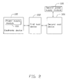
- FIG. 2 illustrates an electronic device assembly in accordance with another embodiment.
- the electronic device assembly can include an electronic device 100, a first load device 200, and a second load device 300.
- the electronic device 100 can include a first power supply module 110 for supplying power to the electronic device 100, the first load device 200, and the second load device 300.
- the first load device 200 can be coupled to the electronic device 100.
- the second load device 300 can be coupled to the first load device 200.
- the second load device 300 can be coupled to a second power supply module 120.
- the electronic device 100, the first load device 200, and the second load device 300 can work cooperatively.
- FIG. 3 illustrates a detail block diagram of the electronic device assembly of FIG. 1 .
- the electronic device 100 can further include a base load 130 and a base output interface 140.
- the base load 130 is coupled to the first power supply module 110.
- the base output interface 140 is coupled to the first power supply module 110.
- the first load 200 can include a first input interface 210, a first output interface 220, a first load 230, a first detecting module 240, and a first switch 250.
- the first input interface 210 is coupled to the first switch 250 and the first detecting module 240.
- the first load 230 is coupled to the first switch 250.
- the first switch 250 is coupled to the first output interface 220.
- the first detecting module 240 is coupled to the first switch 250.
- the first input interface 210 can be matched with the base output interface 140.
- the first input interface 210 and the first output interface 220 can be matched.
- the first input interface 210 of the first load device 200 is coupled to the base output interface 140 of the electronic device 100.
- the first detecting module 240 can detect a first parameter of an input power from the powers supply module 110, and can detect if the first parameter of the input power is greater than a predefined parameter.
- the first switch 250 can be switched on when the first parameter of the input power is greater than the predefined parameter.
- the first load 230 can be powered and the first output interface 220 is electrically connected to the first input interface 210.
- the first switch 250 can be switched off when the first parameter of the input power is not greater than the predefined parameter.
- the first load 230 and the first output interface 220 are disconnected from the first input interface 210.
- the first parameter of the input power can include a voltage value of the input power, a current value of the input power, or a power value of the input power.
- the second load 300 can include a second input interface 310, a second output interface 320, a second load 330, a second detecting module 340, and a second switch 350.
- the second input interface 310 is coupled to the second switch 350 and the second detecting module 340.
- the second load 330 is coupled to the second switch 350.
- the second switch 350 is coupled to the second output interface 320.
- the second detecting module 340 is coupled to the second switch 350.
- the second input interface 310 can be matched with the first output interface 320.
- the second input interface 310 and the second output interface 320 can be matched.
- the second input interface 310 of the second load device 300 is coupled to the first output interface 220 of the first load device 200.
- the second detecting module 340 can detect a second parameter of an input power from first load device 200, and can detect if the second parameter of the input power is greater than the predefined parameter.
- the second switch 350 can be switched on when the second parameter of the input power is greater than the predefined parameter.
- the second load 330 can be powered and the second output interface 320 is electrically connected to the second input interface 310.
- the second switch 350 can be switched off when the second parameter of the input power is not greater than the predefined parameter.
- the second load 330 and the second output interface 320 are disconnected to the second input interface 310.
- the second parameter of the input power can include a voltage value of the input power, a current value of the input power, or a power value of the input power.
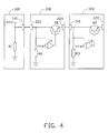
- FIG. 4 illustrates a circuit diagram of the electronic device assembly of FIG. 3 .
- the electronic device 100 can include a base resistor R1.
- the base resistor R1 can be coupled to the power supply module, such as 5V direct current (DC) power source, and can be grounded.
- DC direct current
- the first load device 200 can include a first resistor R2, a first comparator U1, and a first triode Q1.
- the first resistor R2 can be coupled to the first input interface and can be grounded.
- the first detecting module can be the first comparator U1.
- the first comparator U1 can include a first input terminal, a first Vref terminal, and an first output terminal.
- the first input terminal is coupled to the first input interface 210.
- the first output terminal is coupled to the first triode Q 1.
- the first switch can be the first triode Q 1.
- a base of first triode Q1 can be coupled to the first output terminal of the first comparator U1.
- a collector of the first triode Q1 can be coupled to the first input interface 210.
- An emitter of the first triode Q1 can be coupled to the first output interface 220.
- the first triode Q1 can be an NPN-type triode.
- the first input interface 210 of the first load device 200 is coupled to the base output interface 140 of the electronic device 100.
- the first comparator U1 can detect a first voltage of the input power from the power supply module, and can detect if the first voltage of the input power is greater than a Vref voltage.
- the first triode Q1 can be switched on when the first voltage of the input power is greater than the Vref voltage.
- the first load can be powered and the first output interface 220 is electrically connected to the first input interface 210.
- the first switch 250 can be switched off when the first voltage of the input power is not greater than the Vref voltage.
- the first load and the first output interface 220 are disconnected to the first input interface 210.
- the second load device 300 can include a second resistor R3, a second comparator U2, and a second triode Q2.
- the second resistor R3 can be coupled to the second input interface and can be grounded.
- the second detecting module can be the second comparator U2.
- the second comparator U2 can include a second input terminal, a second Vref terminal, and a second output terminal.
- the second input terminal is coupled to the second input interface 310.
- the second output terminal is coupled to the second triode Q2.
- the second switch can be the second triode Q2.
- a base of second triode Q2 can be coupled to the second output terminal of the second comparator U2.
- a collector of the second triode Q2 can be coupled to the second input interface 310.
- An emitter of the second triode Q2 can be coupled to the second output interface 320.
- the second triode Q2 can be an NPN-type triode.
- the second input interface 310 of the second load device 300 is coupled to the first output interface 320.
- the second comparator U2 can detect a second voltage of the input power from the power supply module, and can detect if the second voltage of the input power is greater than the Vref voltage.
- the second triode Q2 can be switched on when the second voltage of the input power is greater than the Vref voltage.
- the second load can be powered and the second output interface 320 is electrically connected to the second input interface 310.
- the second switch 350 can be switched off when the second voltage of the input power is not greater than the Vref voltage.
- the second load and the second output interface 320 are disconnected to the second input interface 310.
Landscapes
- Engineering & Computer Science (AREA)
- Theoretical Computer Science (AREA)
- General Engineering & Computer Science (AREA)
- Physics & Mathematics (AREA)
- General Physics & Mathematics (AREA)
- Computer Hardware Design (AREA)
- Computing Systems (AREA)
- Direct Current Feeding And Distribution (AREA)
- Power Sources (AREA)
Abstract
Description
- This application claims priority to Chinese Patent Application No.
201410062302.1 filed on February 25, 2014 - The subject matter herein generally relates to a load device and an electronic device assembly with the load device.
- Electronic devices, such as computers or monitors, can couple to a plurality of removable load devices, and can supply power to the load devices.
- A load device is coupled to an electronic device. The load device includes a load, an input interface, an output interface, a detecting module, and a switch module. The detecting module can determine if a parameter of an input power from the input interface is greater than a predefined parameter. The switch module is connected to the input interface, the load and the output interface. The switch module can switch off the input power to the load and the output interface when the parameter of the input power from the electronic device is not greater than the predefined parameter.
- Implementations of the present technology will now be described, by way of example only, with reference to the attached figures.
-
FIG. 1 is a block diagram of one embodiment of an electronic device assembly. -
FIG. 2 is a block diagram of another embodiment of an electronic device assembly. -
FIG. 3 is block diagram of another embodiment of the electronic device assembly ofFIG. 1 . -
FIG. 4 is a circuit diagram of the electronic device assembly ofFIG. 3 . - It will be appreciated that for simplicity and clarity of illustration, where appropriate, reference numerals have been repeated among the different figures to indicate corresponding or analogous elements. In addition, numerous specific details are set forth in order to provide a thorough understanding of the embodiments described herein. However, it will be understood by those of ordinary skill in the art that the embodiments described herein can be practiced without these specific details. In other instances, methods, procedures and components have not been described in detail so as not to obscure the related relevant feature being described. Also, the description is not to be considered as limiting the scope of the embodiments described herein. The drawings are not necessarily to scale and the proportions of certain parts may be exaggerated to better illustrate details and features of the present disclosure.
- Several definitions that apply throughout this disclosure will now be presented.
- The term "coupled" is defined as connected, whether directly or indirectly through intervening components, and is not necessarily limited to physical connections. The connection can be such that the objects are permanently connected or releasably connected. The term "comprising," when utilized, means "including, but not necessarily limited to"; it specifically indicates open-ended inclusion or membership in the so-described combination, group, series and the like.
-
FIG. 1 illustrates an electronic device assembly in accordance with a first embodiment. The electronic device assembly can include anelectronic device 100, afirst load device 200, and asecond load device 300. Theelectronic device 100 can be a smart phone, a desktop computer, a laptop computer, a tablet computer, and so on. Theelectronic device 100 can include apower supply module 110 for supplying power to theelectronic device 100, thefirst load device 200, and thesecond load device 300. Thefirst load device 200 and thesecond load device 300 can have the same configuration. Thefirst load device 200 and thesecond load device 300 can be devices similar to theelectronic device 100 or accessories of theelectronic device 100, such as hard disks, or set top boxes. Thefirst load device 200 can be coupled to theelectronic device 100. Thesecond load device 300 can be coupled to thefirst loae device 200. Theelectronic device 100, thefirst load device 200, thesecond load device 300 can work cooperatively. -
FIG. 2 illustrates an electronic device assembly in accordance with another embodiment. The electronic device assembly can include anelectronic device 100, afirst load device 200, and asecond load device 300. Theelectronic device 100 can include a firstpower supply module 110 for supplying power to theelectronic device 100, thefirst load device 200, and thesecond load device 300. Thefirst load device 200 can be coupled to theelectronic device 100. Thesecond load device 300 can be coupled to thefirst load device 200. When the firstpower supply module 110 can not supply enough power to thesecond load device 300, thesecond load device 300 can be coupled to a secondpower supply module 120. Theelectronic device 100, thefirst load device 200, and thesecond load device 300 can work cooperatively. -
FIG. 3 illustrates a detail block diagram of the electronic device assembly ofFIG. 1 . Theelectronic device 100 can further include abase load 130 and abase output interface 140. Thebase load 130 is coupled to the firstpower supply module 110. Thebase output interface 140 is coupled to the firstpower supply module 110. - The
first load 200 can include afirst input interface 210, afirst output interface 220, afirst load 230, afirst detecting module 240, and afirst switch 250. Thefirst input interface 210 is coupled to thefirst switch 250 and thefirst detecting module 240. Thefirst load 230 is coupled to thefirst switch 250. Thefirst switch 250 is coupled to thefirst output interface 220. Thefirst detecting module 240 is coupled to thefirst switch 250. Thefirst input interface 210 can be matched with thebase output interface 140. Thefirst input interface 210 and thefirst output interface 220 can be matched. - The
first input interface 210 of thefirst load device 200 is coupled to thebase output interface 140 of theelectronic device 100. Thefirst detecting module 240 can detect a first parameter of an input power from thepowers supply module 110, and can detect if the first parameter of the input power is greater than a predefined parameter. Thefirst switch 250 can be switched on when the first parameter of the input power is greater than the predefined parameter. Thefirst load 230 can be powered and thefirst output interface 220 is electrically connected to thefirst input interface 210. Thefirst switch 250 can be switched off when the first parameter of the input power is not greater than the predefined parameter. Thefirst load 230 and thefirst output interface 220 are disconnected from thefirst input interface 210. The first parameter of the input power can include a voltage value of the input power, a current value of the input power, or a power value of the input power. - The
second load 300 can include asecond input interface 310, asecond output interface 320, asecond load 330, asecond detecting module 340, and asecond switch 350. Thesecond input interface 310 is coupled to thesecond switch 350 and thesecond detecting module 340. Thesecond load 330 is coupled to thesecond switch 350. Thesecond switch 350 is coupled to thesecond output interface 320. The second detectingmodule 340 is coupled to thesecond switch 350. Thesecond input interface 310 can be matched with thefirst output interface 320. Thesecond input interface 310 and thesecond output interface 320 can be matched. - The
second input interface 310 of thesecond load device 300 is coupled to thefirst output interface 220 of thefirst load device 200. The second detectingmodule 340 can detect a second parameter of an input power fromfirst load device 200, and can detect if the second parameter of the input power is greater than the predefined parameter. Thesecond switch 350 can be switched on when the second parameter of the input power is greater than the predefined parameter. Thesecond load 330 can be powered and thesecond output interface 320 is electrically connected to thesecond input interface 310. Thesecond switch 350 can be switched off when the second parameter of the input power is not greater than the predefined parameter. Thesecond load 330 and thesecond output interface 320 are disconnected to thesecond input interface 310. The second parameter of the input power can include a voltage value of the input power, a current value of the input power, or a power value of the input power. -
FIG. 4 illustrates a circuit diagram of the electronic device assembly ofFIG. 3 . Theelectronic device 100 can include a base resistor R1. The base resistor R1 can be coupled to the power supply module, such as 5V direct current (DC) power source, and can be grounded. - The
first load device 200 can include a first resistor R2, a first comparator U1, and a first triode Q1. The first resistor R2 can be coupled to the first input interface and can be grounded. The first detecting module can be the first comparator U1. The first comparator U1 can include a first input terminal, a first Vref terminal, and an first output terminal. The first input terminal is coupled to thefirst input interface 210. The first output terminal is coupled to the first triode Q 1. The first switch can be the first triode Q 1. A base of first triode Q1 can be coupled to the first output terminal of the first comparator U1. A collector of the first triode Q1 can be coupled to thefirst input interface 210. An emitter of the first triode Q1can be coupled to thefirst output interface 220. The first triode Q1 can be an NPN-type triode. - The
first input interface 210 of thefirst load device 200 is coupled to thebase output interface 140 of theelectronic device 100. The first comparator U1 can detect a first voltage of the input power from the power supply module, and can detect if the first voltage of the input power is greater than a Vref voltage. The first triode Q1 can be switched on when the first voltage of the input power is greater than the Vref voltage. The first load can be powered and thefirst output interface 220 is electrically connected to thefirst input interface 210. Thefirst switch 250 can be switched off when the first voltage of the input power is not greater than the Vref voltage. The first load and thefirst output interface 220 are disconnected to thefirst input interface 210. - The
second load device 300 can include a second resistor R3, a second comparator U2, and a second triode Q2. The second resistor R3 can be coupled to the second input interface and can be grounded. The second detecting module can be the second comparator U2. The second comparator U2 can include a second input terminal, a second Vref terminal, and a second output terminal. The second input terminal is coupled to thesecond input interface 310. The second output terminal is coupled to the second triode Q2. The second switch can be the second triode Q2. A base of second triode Q2 can be coupled to the second output terminal of the second comparator U2. A collector of the second triode Q2 can be coupled to thesecond input interface 310. An emitter of the second triode Q2 can be coupled to thesecond output interface 320. The second triode Q2 can be an NPN-type triode. - The
second input interface 310 of thesecond load device 300 is coupled to thefirst output interface 320. The second comparator U2 can detect a second voltage of the input power from the power supply module, and can detect if the second voltage of the input power is greater than the Vref voltage. The second triode Q2 can be switched on when the second voltage of the input power is greater than the Vref voltage. The second load can be powered and thesecond output interface 320 is electrically connected to thesecond input interface 310. Thesecond switch 350 can be switched off when the second voltage of the input power is not greater than the Vref voltage. The second load and thesecond output interface 320 are disconnected to thesecond input interface 310. - The embodiments shown and described above are only examples. Many details are often found in the art such as the other features of a electronic device assembly. Therefore, many such details are neither shown nor described. Even though numerous characteristics and advantages of the present technology have been set forth in the foregoing description, together with details of the structure and function of the present disclosure, the disclosure is illustrative only, and changes may be made in the detail, including in matters of shape, size and arrangement of the parts within the principles of the present disclosure up to, and including, the full extent established by the broad general meaning of the terms used in the claims. It will therefore be appreciated that the embodiments described above may be modified within the scope of the claims.
Claims (15)
- A load device coupled to an electronic device, the load device comprising:a load;an input interface;an output interface;a detecting module configured to determine if a parameter of an input power from the input interface is greater than a predefined parameter; anda switch module connected to the input interface, the load, and the output interface, and configured to switch off the input power to the load and the output interface when the parameter of the input power from the electronic device is not greater than the predefined parameter.
- The load device of claim 1, wherein the switch module is located between the input interface and the output interface.
- The load device of claim 1, wherein the input interface is configured to matched with the output interface.
- The load device of claim 1, wherein the detecting module comprises a comparator, an input terminal of the comparator is coupled to the input interface, and an output terminal of the comparator is coupled to the switch module.
- The load device of claim 4, wherein the switch module comprises a triode, a base of triode is coupled to the output terminal of the comparator, a collector of the triode is coupled to the input interface, and the emitter of the triode is coupled to the output interface.
- The load device of claim 5, wherein the triode is an NPN-type triode.
- The load device of claim 1, wherein the parameter of the input power comprises a voltage value of the input power.
- The load device of claim 1, wherein the parameter of the input power comprises a current value of the input power.
- The load device of claim 1, wherein the parameter of the input power comprises a power value of the input power.
- The load device of claim 1, further comprising a resistor coupled to the input interface, wherein the resistor is grounded.
- An electronic device assembly comprising:an electronic device; anda load device coupled to the electronic device, the load device configured to receive power from the electronic device, the load device comprising:a load;an input interface coupled to the electronic device;a detecting module configured to determine if a parameter of an input power from the input interface is greater than a predefined parameter; anda switch module connected to the input interface and the load; the switch module configured to switch off the input power to the load when the parameter of the input power from the electronic device is not greater than the predefined parameter.
- The electronic device assembly of claim 11, further comprising an output interface, wherein the switch module is located between the input interface and the output interface.
- The electronic device assembly of claim 12, wherein the input interface is configured to matched with the output interface.
- The electronic device assembly of claim 12, wherein the detecting module comprises a comparator, an input terminal of the comparator is coupled to the input interface, and an output terminal of the comparator is coupled to the switch module.
- The electronic device assembly of claim 14, wherein the switch module comprises a triode, a base of triode is coupled to the output terminal of the comparator, a collector of the triode is coupled to the input interface, and the emitter of the triode is coupled to the output interface.
Applications Claiming Priority (1)
| Application Number | Priority Date | Filing Date | Title |
|---|---|---|---|
| CN201410062302.1A CN104866052A (en) | 2014-02-25 | 2014-02-25 | Power supply system for electronic devices |
Publications (1)
| Publication Number | Publication Date |
|---|---|
| EP2911034A1 true EP2911034A1 (en) | 2015-08-26 |
Family
ID=52146056
Family Applications (1)
| Application Number | Title | Priority Date | Filing Date |
|---|---|---|---|
| EP14195407.3A Withdrawn EP2911034A1 (en) | 2014-02-25 | 2014-11-28 | Load device and electronic device assembly with load device |
Country Status (4)
| Country | Link |
|---|---|
| US (1) | US9606614B2 (en) |
| EP (1) | EP2911034A1 (en) |
| CN (1) | CN104866052A (en) |
| TW (1) | TWI556540B (en) |
Families Citing this family (5)
| Publication number | Priority date | Publication date | Assignee | Title |
|---|---|---|---|---|
| CN107025195A (en) * | 2016-01-30 | 2017-08-08 | 鸿富锦精密电子(重庆)有限公司 | Power supply system of electronic device |
| CN107025194A (en) * | 2016-01-30 | 2017-08-08 | 鸿富锦精密电子(重庆)有限公司 | Power supply system of electronic device |
| CN107272802B (en) * | 2017-06-27 | 2019-02-12 | 苏州佳世达光电有限公司 | Electronic device |
| CN109874314B (en) * | 2017-12-21 | 2021-08-17 | 北京比特大陆科技有限公司 | Series powered circuits, systems and methods |
| CN109976491A (en) * | 2017-12-27 | 2019-07-05 | 鸿富锦精密工业(武汉)有限公司 | Power supply circuit and electronic device including the power supply circuit |
Citations (3)
| Publication number | Priority date | Publication date | Assignee | Title |
|---|---|---|---|---|
| WO2006126160A2 (en) * | 2005-05-22 | 2006-11-30 | Multenet Tecnologies (Pty) Limited | Power and data transmission over ethernet network |
| WO2012148774A2 (en) * | 2011-04-25 | 2012-11-01 | Volterra Semiconductor Corporation | Integrated protection devices with monitoring of electrical characteristics |
| US20120303981A1 (en) * | 2009-11-23 | 2012-11-29 | Jeffrey Lynn Heath | Providing power to powered device having multiple power supply inputs |
Family Cites Families (5)
| Publication number | Priority date | Publication date | Assignee | Title |
|---|---|---|---|---|
| US7349190B1 (en) * | 2003-12-22 | 2008-03-25 | Cypress Semiconductor Corp. | Resistor-less accurate low voltage detect circuit and method for detecting a low voltage condition |
| TWI268414B (en) * | 2004-03-05 | 2006-12-11 | Asustek Comp Inc | Linear voltage stabilizing with a capable of adjusting power distribution having a linear voltage regulator connecting to signal input end and signal output end to adjust input voltage in the mode of power loss and supply stable output voltage |
| AU2005200225A1 (en) * | 2005-01-19 | 2006-08-03 | Opdicom Pty Ltd | Single power source for serially connectable devices |
| KR20100134650A (en) * | 2008-03-10 | 2010-12-23 | 테크티움 엘티디. | Green power supply for converting alternating current into regulated direct current output |
| TWI468895B (en) * | 2012-07-13 | 2015-01-11 | Issc Technologies Corp | Low dropout voltage regulator and electronic device thereof |
-
2014
- 2014-02-25 CN CN201410062302.1A patent/CN104866052A/en active Pending
- 2014-03-03 TW TW103107112A patent/TWI556540B/en not_active IP Right Cessation
- 2014-10-30 US US14/528,355 patent/US9606614B2/en not_active Expired - Fee Related
- 2014-11-28 EP EP14195407.3A patent/EP2911034A1/en not_active Withdrawn
Patent Citations (3)
| Publication number | Priority date | Publication date | Assignee | Title |
|---|---|---|---|---|
| WO2006126160A2 (en) * | 2005-05-22 | 2006-11-30 | Multenet Tecnologies (Pty) Limited | Power and data transmission over ethernet network |
| US20120303981A1 (en) * | 2009-11-23 | 2012-11-29 | Jeffrey Lynn Heath | Providing power to powered device having multiple power supply inputs |
| WO2012148774A2 (en) * | 2011-04-25 | 2012-11-01 | Volterra Semiconductor Corporation | Integrated protection devices with monitoring of electrical characteristics |
Non-Patent Citations (2)
| Title |
|---|
| "3.3-V LDO and Dual Switch For USB Bus-Powered HUB Power Management", 1 August 2001 (2001-08-01), pages 1 - 17, XP055196841, Retrieved from the Internet <URL:http://www.ti.com/lit/gpn/tps2149> [retrieved on 20150618] * |
| "IEEE 802.3af PD Power over Ethernet Interface Controller", 1 January 2003 (2003-01-01), XP055196993, Retrieved from the Internet <URL:http://cds.linear.com/docs/en/datasheet/4257fb.pdf> [retrieved on 20150619] * |
Also Published As
| Publication number | Publication date |
|---|---|
| US20150241953A1 (en) | 2015-08-27 |
| TW201534022A (en) | 2015-09-01 |
| CN104866052A (en) | 2015-08-26 |
| TWI556540B (en) | 2016-11-01 |
| US9606614B2 (en) | 2017-03-28 |
Similar Documents
| Publication | Publication Date | Title |
|---|---|---|
| US9287702B2 (en) | Universal power interface | |
| US9606614B2 (en) | Load device and electronic device assembly with load device | |
| CN106911254A (en) | Electronic device | |
| TWI531144B (en) | Switching power supply circuit | |
| US9651588B2 (en) | Power detecting circuit | |
| US20160299185A1 (en) | Fan detecting device and fan assembly | |
| KR20160092481A (en) | Electronic device and data transmission system | |
| US9557353B2 (en) | Power supply detecting circuit | |
| US20150188344A1 (en) | Charging and discharging control system and method for battery | |
| US9477297B2 (en) | Computer system and matching circuit thereof | |
| US20160072537A1 (en) | Electronic device with wireless module | |
| US20120089763A1 (en) | Computer and usb interface module thereof | |
| CN206619901U (en) | A kind of DC DC power modules and electronic equipment | |
| US9087548B2 (en) | Control circuit for hard disk drive | |
| CN104810868B (en) | Charging system and charging method thereof | |
| US9722444B2 (en) | Electronic device and charging interface | |
| US20160170457A1 (en) | Power control circuit and electronic device | |
| US20150194824A1 (en) | Charge Device and System | |
| US20130151838A1 (en) | Circuit for removing passwords | |
| US20160072276A1 (en) | Overvoltage protection circuit | |
| US20110235219A1 (en) | Protecting device | |
| CN203660580U (en) | Usb charging equipment | |
| US9270161B2 (en) | Power supply circuit for preventing overvoltage | |
| CN108054910A (en) | For electric installation | |
| CN104600961A (en) | Power supply device, power supply system and method for controlling said system |
Legal Events
| Date | Code | Title | Description |
|---|---|---|---|
| PUAI | Public reference made under article 153(3) epc to a published international application that has entered the european phase |
Free format text: ORIGINAL CODE: 0009012 |
|
| AK | Designated contracting states |
Kind code of ref document: A1 Designated state(s): AL AT BE BG CH CY CZ DE DK EE ES FI FR GB GR HR HU IE IS IT LI LT LU LV MC MK MT NL NO PL PT RO RS SE SI SK SM TR |
|
| AX | Request for extension of the european patent |
Extension state: BA ME |
|
| 17P | Request for examination filed |
Effective date: 20160225 |
|
| RBV | Designated contracting states (corrected) |
Designated state(s): AL AT BE BG CH CY CZ DE DK EE ES FI FR GB GR HR HU IE IS IT LI LT LU LV MC MK MT NL NO PL PT RO RS SE SI SK SM TR |
|
| 17Q | First examination report despatched |
Effective date: 20160725 |
|
| STAA | Information on the status of an ep patent application or granted ep patent |
Free format text: STATUS: EXAMINATION IS IN PROGRESS |
|
| APBK | Appeal reference recorded |
Free format text: ORIGINAL CODE: EPIDOSNREFNE |
|
| APBN | Date of receipt of notice of appeal recorded |
Free format text: ORIGINAL CODE: EPIDOSNNOA2E |
|
| APBR | Date of receipt of statement of grounds of appeal recorded |
Free format text: ORIGINAL CODE: EPIDOSNNOA3E |
|
| APAF | Appeal reference modified |
Free format text: ORIGINAL CODE: EPIDOSCREFNE |
|
| APBT | Appeal procedure closed |
Free format text: ORIGINAL CODE: EPIDOSNNOA9E |
|
| STAA | Information on the status of an ep patent application or granted ep patent |
Free format text: STATUS: THE APPLICATION IS DEEMED TO BE WITHDRAWN |
|
| 18D | Application deemed to be withdrawn |
Effective date: 20200603 |