EP2908095A1 - Sun sensor for determining a position of the sun relative to an object - Google Patents
Sun sensor for determining a position of the sun relative to an object Download PDFInfo
- Publication number
- EP2908095A1 EP2908095A1 EP14000559.6A EP14000559A EP2908095A1 EP 2908095 A1 EP2908095 A1 EP 2908095A1 EP 14000559 A EP14000559 A EP 14000559A EP 2908095 A1 EP2908095 A1 EP 2908095A1
- Authority
- EP
- European Patent Office
- Prior art keywords
- detector
- sun
- sensor according
- sun sensor
- detector surface
- Prior art date
- Legal status (The legal status is an assumption and is not a legal conclusion. Google has not performed a legal analysis and makes no representation as to the accuracy of the status listed.)
- Granted
Links
Images


Classifications
-
- G—PHYSICS
- G01—MEASURING; TESTING
- G01C—MEASURING DISTANCES, LEVELS OR BEARINGS; SURVEYING; NAVIGATION; GYROSCOPIC INSTRUMENTS; PHOTOGRAMMETRY OR VIDEOGRAMMETRY
- G01C17/00—Compasses; Devices for ascertaining true or magnetic north for navigation or surveying purposes
- G01C17/34—Sun- or astro-compasses
-
- B—PERFORMING OPERATIONS; TRANSPORTING
- B64—AIRCRAFT; AVIATION; COSMONAUTICS
- B64G—COSMONAUTICS; VEHICLES OR EQUIPMENT THEREFOR
- B64G1/00—Cosmonautic vehicles
- B64G1/22—Parts of, or equipment specially adapted for fitting in or to, cosmonautic vehicles
- B64G1/24—Guiding or controlling apparatus, e.g. for attitude control
- B64G1/36—Guiding or controlling apparatus, e.g. for attitude control using sensors, e.g. sun-sensors, horizon sensors
- B64G1/363—Guiding or controlling apparatus, e.g. for attitude control using sensors, e.g. sun-sensors, horizon sensors using sun sensors
Definitions
- the invention relates to a sun sensor for determining a position of the sun relative to an object, in particular for use in an attitude and orbit control system of a spacecraft, with at least one detector.
- Sun sensors are an essential element of an attitude and orbit control system (AOCS) of almost every satellite.
- AOCS attitude and orbit control system
- the majority of used analogue sun sensors are based on photo-diodes which measure the solar flux projected onto a detector surface and generate a corresponding photo-current I [9].
- FIG. 1 schematically illustrates a diagram of a conventional photo-detector of an analogue sun sensor: Sun rays 100 are incident on a detector surface 102 (photocell) at an angle ⁇ , leading to a modulation of a photo-current according to equation (1).
- the incident angle ⁇ is constituted between the surface normal vector 104 and the direction of the solar rays 100.
- a mask 106 is arranged in front of the detector surface 102 .
- the mask 106 allows a part of the solar rays to pass through the mask to incident on the detector surface 102.
- the sensitivity coefficient K s describes how sensitive the detector output current is towards small changes of the incidence angle ⁇ . From a detailed analysis it can be shown that a high sensitivity to angular changes implies a large robustness to fluctuations in the intensity of the incident light and to overall gain variations.
- the coefficient K s can either be defined in terms of angular sensitivity relative to the angle of normal incidence or in terms of angular sensitivity relative to the actual angle of incidence.
- the sensitivity K s is always ⁇ 1 for a cosine detector.
- the cosine detector relies on a mere geometric projection resulting in low measurement precision.
- a sun sensor for determining a position of the sun relative to an object, in particular for use in an attitude and orbit control system of a spacecraft, where at least one detector is provided.
- Each of the detectors comprises a metal substrate constituting at least one detector surface and emitting electrons upon exposure to UV-light; a receiving anode for collecting the electrons emitted by the metal substrate; a current sensing means for measuring a current that is generated by the electrons which are emitted by the cathode; and a processing unit for evaluating the current measured by the current sensing means, wherein the processing unit is adapted to determine a position of the sun relative to the object by determining an incidence angle of solar rays from an amount of the evaluated current.
- the sun sensor according to the invention makes use of the well-known "vectorial photoelectric effect” [2], [3].
- This effect is essentially based on greater emission efficiency for light with a polarization component normal to the surface than for light with a polarization component parallel to the surface. Only p-polarized light, for which the polarization vector lies in the plane of incidence, has such a normal component.
- the polarization component normal to the surface of p-polarized light increases with increasing incidence angle ⁇ , which in turn leads to a large rise in emission efficiency.
- the sensitivity of photo-emission to variations in the incidence angle constitutes the basis for what can be referred to as a "Vectorial photoelectric effect (VPE) detector".
- VPE Vectorial photoelectric effect
- the metal is selected from a material having a vectorial photo-electric effect.
- the metal may be selected from a noble metal, in particular gold.
- the substrate may be made from the metal to represent the detector surface.
- the substrate may comprise a bulk material which is coated with the metal.
- the substrate may form an integral building block for various types of sun sensors. The substrate can be easily scaled for any application requirement. The substrate makes the detector very robust regarding to degradation and ageing effects.
- At least one detector surface may be encapsulated in a housing.
- the detector of the sun sensor may be encapsulated in a sealed housing or a bulb on ground.
- ground packaged and/or sealed detectors may consist of COTS (Au) photocathodes or customized detector surfaces that can be sealed on ground to be protected against possible contamination sources on ground or in space.
- At least one detector surface may be arranged in a free-to-space-configuration. That means that the detector surface is directly exposed to its environment. Although such an arrangement is sensitive to potential surface contaminations, these are mitigated by the cleaning effect due to a strong UV illumination [10],[11],[12], as well as due the residual concentrations of atomic oxygen at high altitudes.
- a polarization filter may be arranged in front of the at least one detector surface.
- the usage of a polarization filter increases the detection sensitivity of the sun sensor (and therefore spacecraft) attitude with respect to the sun. If only p-polarized light is incident on the detector surface, the sensor sensitivity can be increased (on cost of lower detection currents).
- an optical window filter may be arranged in front of the at least one detector surface.
- the usage of an optical window filter increases the detection sensitivity of the sensor, i.e. the detector (and therefore object, e.g. a spacecraft) attitude with respect to the sun.
- the at least one detector surface may be arranged parallel with respect to a detector window.
- the at least one detector surface may be inclined with respect to a detector window. Applying an inclination of the detector surface(s) with respect to a detector window and an optional transmission mask increases the detection sensitivity of the sensor (and therefore object, e.g. a spacecraft) attitude with respect to the sun.
- a voltage source for providing a negative bias voltage to the at least one detector surface may be provided. Applying a negative bias voltage on the detector surface and, at the same time, the collector at object (spacecraft) reference ground potential prevents the detector to collect electrons from other sources.
- the receiving anode may be arranged above the at least one detector surface while having a predetermined distance to the at least one detector surface.
- the usage of an electron collector above the sensor surface, i.e. the metal substrate, allows establishing a well-defined electrical circuit which is robust against absolute potentials and potential variations of the object, e.g. the spacecraft.
- the receiving anode may be made from a wire mesh.
- VPE detectors vectorial photoelectric effect detectors
- the individual VPE detector can form an integral building block for various types of sun sensors which - similar to existing cosine detector arrangements - can form combinations between several VPE detectors.
- VPE detectors over conventional cosine detectors, if used in sun sensors, are:
- VPE detector The basic principle of a VPE detector is as follows:
- sun detector comprising at least one VPE detector
- a total solar flux of 1384 W/m 2 incident on a satellite close to earth can be found.
- the solar flux contribution above the cut-off energy is found to be 0.80 % of the total solar flux energy from integrating the solar flux from a frequency corresponding to an energy of 5.1 eV to infinity. This corresponds to a total power 1.11 mW of UV light above 5.1 eV incident on a 1 cm x 1 cm surface area.
- Quantum Yield is the number of photo-electrons emitted per absorbed photon.
- Quantum Efficiency is the number of photo-electrons emitted per incident photon.
- the photoelectric emission is generally considered as coming from the material bulk. Whereas the detailed atomic lattice structure and the corresponding energy bands are important and determine detailed features of the photoemission process, it is possible to obtain an approximation of the quantum efficiency by Fowler's law [1], [4]. It describes the dependence of the Quantum Efficiency (QE) on the frequency v of the incident light and is generally a reasonably good approximation.
- ⁇ p ⁇ and ⁇ p0 are the absorbed energy of p-polarized incident light normal and parallel to the surface, respectively
- ⁇ s is the absorbed energy of s-polarized incident light.
- Equation (12) p-polarized light has a component parallel to the surface and a component normal to the surface. The distinction between these components is crucial, as a much higher efficiency to the normal component than to the parallel one (see Equation (12) is attributed. It is therefore assumed that the amount of absorbed p-polarized light with orthogonal polarization is proportional to the energy ratio of p-polarized light with orthogonal polarization to the total amount of p-polarized light, as expressed in Equation 18. The same reasoning applies to p-polarized light with parallel polarization, as expressed in Equation 19.
- ⁇ p ⁇ ⁇ ⁇ p ⁇ 0 1 - R p ⁇ 1 - R p 0 ⁇ E p ⁇ ⁇ 2
- 2 + E p ⁇ ⁇ 2 ⁇ p ⁇ ⁇ ⁇ p ⁇ 0 1 - R p ⁇ 1 - R p 0 ⁇ E p ⁇ ⁇ 2
- Equation (22) The expression for the yield of s-polarized light can be combined with the one for p-polarized light to obtain Equation (22) (which could alternatively be derived from Equation (9):
- QE ⁇ QE 0 1 - R ⁇ 1 - R 0 + r - 1 ⁇ 1 - R p ⁇ 1 - R p 0 ⁇ E p ⁇ ⁇ 2
- Equations (20), (21) and (22) are used in Equations (20), (21) and (22) to obtain Figure 4 , which plots the normalized quantum efficiencies for different polarization types 402, 404, 406, 408 of light with energy 5.44 eV.
- Variation of the index of refraction with wavelength The complex index of refraction changes with wavelength.
- the necessary material properties were found in [6] for gold and copper.
- the real part of the complex index of refraction is the refractive index n whereas the imaginary part is the extinction coefficient k.
- Both parameters are plotted for gold and copper over a wavelength range corresponding to 5.1 eV to 11 eV photon energies in Figure 8.
- Figure 8 illustrates the index of refraction for copper (solid lines 802, 804) and gold (dotted lines 806, 808) over a wavelength range corresponding to photon energies from 5.1 eV to 11 eV.
- the lines 802, 808 correspond to the refractive index and the lines 804, 808 to the extinction coefficients.
- the data points used to re-produce the measurement data in [4] are given by the open circles 810 and 812.
- Equation (26) QE of p-polarized light is obtained:
- Equation (27) shows that the total emission comprises a part from the bulk and a part from p-polarized light normal to the surface that is enhanced by a factor of (r-1) with respect to the bulk emission.
- the index of refraction enters many of those quantities. It is therefore important to know its variation over the entire region of interest, which is shown in Figure 8 .
- Equation (30) The calculation of the total photo-current, as described by Equation (30), depends on certain frequency-dependent parameters. These include the cooperativity parameter 'r' of Equation (12), the reflectivity'Rp' of Equation (15), the parameter's' defined in Equation (14), and the quantum efficiency for bulk emission of Equation (6), which are all known at this point.
- the vectorial photoelectric effect additionally contributes to the emission process and generates much higher total emission currents.
- the cooperativity parameter r decreases rapidly with increasing photon energy so that it is mainly the photons of lower energies (up to 1 eV above the work function ⁇ AU ) that contribute to the sensitivity.
- the solid line 1002 in Figure 10 indicates the emission current for p-polarized light when the full spectrum from threshold at 5.1 eV up to 11 eV is integrated.
- the solid line 1006 is the result for integration of the spectrum up to 0.5 eV above threshold. While the absolute values of the emission current are smaller when an energy cutoff is chosen (only up to 1.3 milli Ampere per square meter of detector area instead of 6 mA for no cutoff), the sensitivity to the incidence angle is increased. This is because primarily photons with energies close to the threshold contribute to the vectorial photoelectric effect, whereas photons of higher energy only contribute to the bulk emission and tend to dilute the overall sensitivity.
- Figure 11 shows a different representation of the data in Figure 10 .
- the plot gives the emission current normalized by its value at normal incidence.
- the crosses indicate approximations with a sin 2 law of Equation (23).
- the cut-off total emission current has a slope that is a factor of 9.1973/0.2805 ⁇ 33 larger than the cut-off bulk emission current.
- VPE detector in a sun sensor will be described together with exemplary embodiments of the invention. Before, a comparison between a VPE detector and a cosine detector will be made.
- B - 16 for p-polarized light and a cutoff of 0.5 eV above threshold see table 2
- Figure 12 shows the (normalized) photo-emission currents for light cut-off at 0.5 eV above threshold which is given by the solid line 1202.
- the crosses 1204 are the analytical approximation according to Equation (23).
- the geometric projection is accounted for in the VPE currents.
- the cosine detector response is given as solid line 1206.
- the proposed sun sensor consists of a metal (in particular gold) substrate that may either be directly be exposed to the void of space (reliant on UV cleaning to mitigate contamination) or encased in a vacuum packaging (reliant on sealed environment to avoid contamination). In the latter, the design would then be similar to that of a standard photo-cathode, such as those produced by Hamamatsu [17].
- the dimension of the available packaging is typically 10 mm to 15 mm in diameter and 30 mm in length (see Figure 14a , which shows Hamamatsu phototubes). In Figure 14b dimensions of the Hamamatsu phototube containing a gold cathode are figured out.
- Emitted electrons are collected with a receiving anode 1506, 1605. This can be accomplished by placing above the detector surface 1502; 1602, 1604 a wire mesh that largely transmits the incident light and collects the emitted electrons.
- the used detector surface material may be any metal where the vectorial photo-electric effect occurs and is sufficiently strong.
- Known materials where the vectorial photo-electric effect occurs are e.g. copper [4] or silicon [2].
- the crystalline symmetry is not important for the vectorial photo-electric effect. It was shown that the effect is the same for single crystal copper as for polycrystal copper [3].
- VPE vectorial photo-effect
- the first configuration implements a single metal cathode 1501 in a housing 1520 of the detector 1500.
- the anode mesh 1506 that collects the emitted photo-electrons is shown some distance above the cathode 1501.
- the whole package is covered by a fused silica window 1508 which may also include polarizer and transmission filter.
- the window 1508 is arranged on a mask 1504 having an aperture 1516 to allow solar rays 1510 to incide on the cathode 1501 and its cathode surface, respectively.
- the cathode 1501 and the anode 1506 are connected to a respective voltage connection 1514 and 1512, respectively.
- two sensitive detector surfaces (cathode surfaces) 1602, 1604 of detectors (cathodes) 1601, 1603 are inclined by approximately 50-60 degrees with respect to the detector window 1609 and transmission mask 1608, as shown in Figure 16 .
- this embodiment provides two detectors in a housing 1620 where both are inclined with respect to the sun at normal incidence.
- An anode mesh 1605 collects the emitted photo-electrons.
- the anode mesh 1605 is bent around the two cathodes 1601, 1603.
- the whole package is covered by a fused silica window 1609 which may also include polarizer and transmission filter.
- the window 1609 is arranged on a mask 1606 having two apertures 1607 and 1608 to allow solar rays 1610, 1614 to incide on the cathodes 1601, 1603 and its cathode surfaces 1602, 1604, respectively.
- each of the cathodes 1601, 1603 and the bent anode mesh 1605 are connected to respective voltage connection 1611, 1612 and 1613, respectively.
- the geometric projection effect reinforces the vectorial photo-effect rather than offsetting it (see also Figure 13 ).
- Table 3 illustrates important (default) operating parameters of a VPE-based sun sensor.
- the middle column reflects typical (default values), the right-most column the range of values which is expected depending on specific design choices.
- UV fused silica windows transmit light down to wavelengths of around 185 nm.
- Thorlabs quotes the UVFS window transmission shown in Figure 17 for an uncoated fused silica substrate of 10 mm [14].
- Alternative substrates made from Magnesium Fluoride (MgF2), Sapphire, and Calcium Fluoride (CaF2) may also be used.
- Figure 18 illustrates the ideal UV window for the VPE detector transmits light between 243 nm and 221 nm before dropping to zero transmission at higher wavelengths.
- the ideal window transmission would therefore resemble the curve 1802 of Figure 18 , whereas the acceptable range of transmission profiles is indicated by the area 1804. Curves that lie within that range result in sensitivity curves close the ideal case on the one hand, and account for realistic material properties on the other hand.
- the required drop in transmission for wavelengths smaller than 221 nm can be achieved by applying a reflective coating on the window which is optimized to obtain high reflectivity at wavelengths around 203 nm but drops off towards higher wavelengths to transmit in the range 221-243 nm.
- a reflective coating on the window which is optimized to obtain high reflectivity at wavelengths around 203 nm but drops off towards higher wavelengths to transmit in the range 221-243 nm.
- Such custom coatings could be applied e.g. by Elliot scientific [15].
- Other manufacturers, such as AHF Filters [16] provide suitable razor-edge filters.
- An example filter with a cutoff at at 229 nm from AHF is shown in Figure 19 .
- the VPE operates with maximal sensitivity, if p-polarized light is incident on the surface. This can be ensured by the use of a polarizer. In order to optimally exploit this effect, two requirements must be fulfilled: The light must be linearly polarized and the plane of incidence must lie in the plane defined by the polarizer axis and the sensor surface normal.
- a polarizer 2002 placed above the detector surface 2004 acts as a natural selector of a sensitive incidence plane.
- the detector 2004 is then primarily sensitive to angular changes of the incident light in a plane that is spanned by the polarizer axis 2006 and the surface normal 2008. This is depicted in Figure 20 . If, on the other hand, the incidence plane is normal to the image plane of Figure 20 , the transmitted light is s-polarized, which leads to reduced emission currents compared to p-polarized light.
- the polarizer ensures that the detector is sensitive to light in the plane of incidence spanned by polarizer axis and surface normal.
- Polarizers in the deep UV are produced by several companies, for example Meadowlark [13]. These polarizers are based on dielectric nanowire arrays, where the substrate is made from fused silica and the wire-grid from dielectric material rather than metal to give high damage thresholds and avoid oxidization.
- the wire-grid polarizer characteristics as quoted by Meadowlark [13] are given in Figure 21 . It shows typical transmission (curve 2102) and contrast ratio (curve 2104) versus wavelength over the usable wavelength range for nanowire polarizers.
- the extinction ratios for short wavelengths around 240 nm are typically only about 1:50. This is not very large but easily sufficient for use in a spacecraft. Also note that the transmission drops to approximately 70% for these wavelengths, which is still sufficiently large.
- the VPE-detector resembles a photo-cathode and outputs a current which must be converted into a voltage that is then fed to a remote-interface-unit (RIU), i.e. a processing unit, of the spacecraft.
- ROU remote-interface-unit
- This is achieved using a transimpedance amplifier circuit with an operational amplifier 2202 (OpAmp) at its core.
- the bias voltage 2204 for the VPE-detector can at the same time be used as a supply voltage for the OpAmp 2202.
- An example for an operating circuit is given in Figure 22 .
Landscapes
- Engineering & Computer Science (AREA)
- Remote Sensing (AREA)
- Radar, Positioning & Navigation (AREA)
- Physics & Mathematics (AREA)
- Astronomy & Astrophysics (AREA)
- General Physics & Mathematics (AREA)
- Chemical & Material Sciences (AREA)
- Combustion & Propulsion (AREA)
- Aviation & Aerospace Engineering (AREA)
- Photometry And Measurement Of Optical Pulse Characteristics (AREA)
Abstract
Description
- The invention relates to a sun sensor for determining a position of the sun relative to an object, in particular for use in an attitude and orbit control system of a spacecraft, with at least one detector.
- Sun sensors are an essential element of an attitude and orbit control system (AOCS) of almost every satellite. The majority of used analogue sun sensors are based on photo-diodes which measure the solar flux projected onto a detector surface and generate a corresponding photo-current I [9]. The current I is proportional to incidence angle Θ between the surface normal vector and the direction of the solar rays, as given by Equation (1)

-
Figure 1 schematically illustrates a diagram of a conventional photo-detector of an analogue sun sensor:Sun rays 100 are incident on a detector surface 102 (photocell) at an angle Θ, leading to a modulation of a photo-current according to equation (1). The incident angle Θ is constituted between the surfacenormal vector 104 and the direction of thesolar rays 100. In front of the detector surface 102 amask 106 is arranged. Themask 106 allows a part of the solar rays to pass through the mask to incident on thedetector surface 102. - Various implementations and model configurations of sun sensors combine or subtract the photo-current from several photo-cells in specific geometric arrangements, which optimizes and custom tailors the sun sensor to the specific application requirements [9]. However, in most cases the various configurations rely on the same basic principle of a "cosine detector", as outlined above in Equation (1). The sensitivity coefficient Ks describes how sensitive the detector output current is towards small changes of the incidence angle Θ. From a detailed analysis it can be shown that a high sensitivity to angular changes implies a large robustness to fluctuations in the intensity of the incident light and to overall gain variations. The coefficient Ks can either be defined in terms of angular sensitivity relative to the angle of normal incidence or in terms of angular sensitivity relative to the actual angle of incidence.
- Adopting the former definition, the coefficient Ks is written as the derivative of the current with respect to Θ, normalized by the current at normal incidence:

- As can be seen from Equation (2), the sensitivity Ks is always ≤1 for a cosine detector. Hence, the cosine detector relies on a mere geometric projection resulting in low measurement precision.
- It is the object of the present invention to provide a sun sensor for determining a position of the sun relative to an object, in particular for use in an attitude and orbit control system of a spacecraft, being insensitive to albedo and having an improved accuracy, which leads to less sensitivity to fluctuations of solar irradiance and sensor gain variations.
- These objects are solved by a sun sensor according to the features of
claim 1. Preferred embodiments are set out in the dependent claims. - According to an aspect of the invention, a sun sensor for determining a position of the sun relative to an object, in particular for use in an attitude and orbit control system of a spacecraft, where at least one detector is provided. Each of the detectors comprises a metal substrate constituting at least one detector surface and emitting electrons upon exposure to UV-light; a receiving anode for collecting the electrons emitted by the metal substrate; a current sensing means for measuring a current that is generated by the electrons which are emitted by the cathode; and a processing unit for evaluating the current measured by the current sensing means, wherein the processing unit is adapted to determine a position of the sun relative to the object by determining an incidence angle of solar rays from an amount of the evaluated current.
- The sun sensor according to the invention makes use of the well-known "vectorial photoelectric effect" [2], [3]. This effect is essentially based on greater emission efficiency for light with a polarization component normal to the surface than for light with a polarization component parallel to the surface. Only p-polarized light, for which the polarization vector lies in the plane of incidence, has such a normal component. The polarization component normal to the surface of p-polarized light increases with increasing incidence angle Θ, which in turn leads to a large rise in emission efficiency. The sensitivity of photo-emission to variations in the incidence angle constitutes the basis for what can be referred to as a "Vectorial photoelectric effect (VPE) detector".
- According to a preferred embodiment, the metal is selected from a material having a vectorial photo-electric effect. In particular, the metal may be selected from a noble metal, in particular gold.
- In one alternative the substrate may be made from the metal to represent the detector surface. In another alternative, the substrate may comprise a bulk material which is coated with the metal. For example, the substrate may form an integral building block for various types of sun sensors. The substrate can be easily scaled for any application requirement. The substrate makes the detector very robust regarding to degradation and ageing effects.
- According to a preferred embodiment, at least one detector surface may be encapsulated in a housing. For example, the detector of the sun sensor may be encapsulated in a sealed housing or a bulb on ground. Furthermore, ground packaged and/or sealed detectors may consist of COTS (Au) photocathodes or customized detector surfaces that can be sealed on ground to be protected against possible contamination sources on ground or in space.
- Alternatively, at least one detector surface may be arranged in a free-to-space-configuration. That means that the detector surface is directly exposed to its environment. Although such an arrangement is sensitive to potential surface contaminations, these are mitigated by the cleaning effect due to a strong UV illumination [10],[11],[12], as well as due the residual concentrations of atomic oxygen at high altitudes.
- According to a further preferred embodiment, a polarization filter may be arranged in front of the at least one detector surface. The usage of a polarization filter increases the detection sensitivity of the sun sensor (and therefore spacecraft) attitude with respect to the sun. If only p-polarized light is incident on the detector surface, the sensor sensitivity can be increased (on cost of lower detection currents).
- According to a further preferred embodiment, an optical window filter may be arranged in front of the at least one detector surface. The usage of an optical window filter increases the detection sensitivity of the sensor, i.e. the detector (and therefore object, e.g. a spacecraft) attitude with respect to the sun.
- According to a further preferred embodiment, the at least one detector surface may be arranged parallel with respect to a detector window.
- Alternatively, the at least one detector surface may be inclined with respect to a detector window. Applying an inclination of the detector surface(s) with respect to a detector window and an optional transmission mask increases the detection sensitivity of the sensor (and therefore object, e.g. a spacecraft) attitude with respect to the sun.
- According to a further preferred embodiment, a voltage source for providing a negative bias voltage to the at least one detector surface may be provided. Applying a negative bias voltage on the detector surface and, at the same time, the collector at object (spacecraft) reference ground potential prevents the detector to collect electrons from other sources.
- According to a further embodiment, the receiving anode may be arranged above the at least one detector surface while having a predetermined distance to the at least one detector surface. The usage of an electron collector above the sensor surface, i.e. the metal substrate, allows establishing a well-defined electrical circuit which is robust against absolute potentials and potential variations of the object, e.g. the spacecraft.
- The receiving anode may be made from a wire mesh.
- Summarizing, the invention proposes to use "vectorial photoelectric effect" detectors (VPE detectors) instead of conventional cosine detectors in analogue sun sensors. Therefore, the individual VPE detector can form an integral building block for various types of sun sensors which - similar to existing cosine detector arrangements - can form combinations between several VPE detectors.
- Advantages of VPE detectors over conventional cosine detectors, if used in sun sensors, are:
- Sensitivity: A VPE detector has a larger sensitivity of photo-current on changes of incidence angle. An improvement by factor ~10-20 is expected.
- Albedo correction: Conventional sun sensors are based on cosine detectors that operate in the visible spectrum and therefore require an earth albedo correction for precise angular measurements. In contrast, the VPE detector relies on UV-light with wavelengths below 300 nm and is therefore insensitive to the earth albedo.
- Lifetime: The detector lifetime is expected to be longer, as the metal (e.g. gold) coated surfaces of a VPE detector are less sensitive to radiation from highly energetic particles (protons, electrons) than conventional silicon-based detectors. This opens opportunities for preferred use in space missions closer to the sun where radiation levels can be considerably higher and material aging is considerably worse than close to earth.
- Degradation: Only insignificant aging and few degradation effects are expected if the VPEs are based on gold-coated substrates. Gold is chemically quite inert and the surfaces therefore do not easily oxidize, which could otherwise considerably impair the vectorial photoelectric emission efficiency [2]. Additionally, gold surfaces that are strongly illuminated by UV-light display a cleaning effect. This can mitigate potential sensor surface contaminations.
- Detector gain variations: Little change of detector gain and the corresponding calibration curve over time are expected, due to the small degradation. In contrast, the gain of silicon-based detectors may degrade by 10% or more over their lifetime.
- Ease of manufacture: VPE detectors are easy to manufacture, in particular easy to scale in size and geometry. Detector areas on the order of tens of square centimeters can be manufactures as easily as smaller ones (1 cm2 baseline).
- The invention will be described in more detail by reference to the accompanying figures.
- Figure 1
- shows a schematically diagram of a conventional photo-detector as a core element of an analogue sun sensor.
- Figure 2
- shows a comparison of normalized sensitivities (i.e. photo-currents) of a cosine detector and a generic VPE detector.
- Figs. 3a, 3b
- show the solar spectral intensity plotted against the radiation energy at a distance of 150 million km from the sun, wherein
Fig. 3a shows a full spectrum andFig 3b shows a spectral zoom into a selected region. - Figure 4
- shows the normalized quantum efficiency plotted for light of energy hv = 5.44 eV and various polarizations.
- Figure 5
- shows the quantum efficiency (QE) of p-polarized light for the total emission and the bulk emission.
- Figure 6:
- shows cooperativity parameters for three measurements of Perdersoli [4] plotted against the difference ΔE between the radiation energy and the work function of copper φ=4.94 eV, i.e. against ΔE=hv-Φ).
- Figure 7
- shows the measured quantum efficiencies normalized by the amount of absorbed light (1-R) for three different energies.
- Figure 8
- shows the index of refraction plotted for copper and gold over a wavelength range corresponding to photon energies from 5.1 eV to 11 eV.
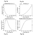
- Figs. 9a to 9d
- show photon flux, quantum efficiency, emitted electron flux, and cumulative emission current which are plotted against photon energy for 0° incidence angle of the light.
- Figure 10
- shows emission currents as a function of incidence angle for the case that all photon energies above the threshold are considered and for the case that only photons up to 0.5 eV above threshold are considered.
- Figure 11
- shows a different representation of the data in
Figure 10 , in which the emission current normalized by its value at normal incidence is illustrated. - Figure 12
- shows (normalized) photo-emission currents for light cut-off at 0.5 eV above a given threshold.
- Figure 13
- shows quantum efficiency, geometric projection factor, and the product thereof for a tilted VPE detector.
- Figure 14a
- shows a photo of Hamamatsu phototubes.
- Figure 14b
- shows dimensions of the Hamamatsu phototube containing a gold cathode.
- Figure 15
- shows a first embodiment of a single VPE detector used as a sun sensor.
- Figure 16
- shows a second embodiment of a sun sensor according to the invention having two detectors where both are inclined with respect to the sun at normal incidence.
- Figure 17
- shows the transmission through an uncoated fused silica substrate of 10 mm thickness.
- Figure 18
- shows an ideal UV window for the VPE detector that transmits light between 243 nm and 221 nm before dropping to zero transmission at higher wavelengths.
- Figure 19
- shows a Raman emitter filter with a cutoff at 229 nm.
- Figure 20
- shows a polarizer ensuring that the detector is sensitive to light in the plane of incidence spanned by polarizer axis and surface normal.
- Figure 21
- shows typical transmission and contrast ratio versus wavelength over the usable wavelength range for nanowire polarizers.
- Figure 22
- shows a schematic of an operating circuit used for a VPE detector according to the invention.
- The basic principle of a VPE detector is as follows:
- Assuming that UV-light is incident on a metal-coated, in particular a gold-coated, substrate surface, the quantum efficiency for the emission of photo-electrons is given by Equation (3) for angles between -60° to +60°:

- As will become apparent by the description of how the photo-currents for the VPE detector are calculated, a value of B ~ 16 is obtained for the sensitivity parameter B of Equation (3) under certain assumptions. This leads to strongly increasing photo-currents with increasing incidence angle in VPE detectors. They are therefore much more sensitive to changes of the light incidence angle than standard cosine detectors. Depending on the detector geometry, the slope of the sensitivity curve may be up to 20 times larger than for a cosine detector.
- In
Figure 2 , the variation of quantum efficiency for a generic VPE detector (200) is plotted together with thesensitivity curve 202 for the cosine detector for the sake of comparison. An analytical approximation according to Equation (3) is given by thecrosses 204 for angles <60°. The sensitivities are normalized and represent photo-currents. Whereas thesolid line 200 was found from detailed numerical calculations, thecrosses 204 indicate an analytical approximation according to Equation (3). - In the following section a detailed description of how the photo-currents for the VPE detectors are calculated will be described together with a derivation of underlying formulae and required background information. Furthermore, pertinent assumptions leading to calculation of the photo-current curve for the VPE detector are discussed.
- Afterwards, embodiments of a sun detector comprising at least one VPE detector will be described.
- An expression for the energy radiated by an ideal black-body per unit area and per unit time within a frequency interval (v, v + dv) is given as:

where v is the frequency, kB is Boltzmann's constant, T the temperature of the black-body, and h is Planck's constant. Integrating over the frequency, Stefan's law is obtained:
- Based on Equation (4), in
Figure 3a thefull energy spectrum 300 of the sun is plotted against the radiation energy in units of [eV] at a distance of 150 million km from the sun. The cutoff at 5.1 eV, corresponding to the work function of gold, is given by thecircle 302. InFigure 3b , a spectral zoom into the region above cut-off is shown. A temperature of 5780 K was assumed for the sun. The fact that the spectrum is assumed to be recorded at 1 au (~150 million km) from the sun requires multiplying the integrand of Equation (4) by a factor F equal to the squared ratio between sun radius Rsun and the distance to earth: F = (Rsun/au)2. - It is preferred to use a substrate coated with gold for the VPE detector, only solar radiation above the work function of gold, ΦAu=5.1 eV (
circle 302 inFigs. 3a and3b ), affects the emission of photo-electrons. The contributions of the spectrum above this cut-off are given by the high energy tail ofFigs. 3 . - Integrating the full spectrum from 0 to infinity, a total solar flux of 1384 W/m2 incident on a satellite close to earth can be found. The solar flux contribution above the cut-off energy is found to be 0.80 % of the total solar flux energy from integrating the solar flux from a frequency corresponding to an energy of 5.1 eV to infinity. This corresponds to a total power 1.11 mW of UV light above 5.1 eV incident on a 1 cm x 1 cm surface area.
- For establishing the photoelectric effect for bulk emission, the following definitions are given: The Quantum Yield (QY) is the number of photo-electrons emitted per absorbed photon. The Quantum Efficiency (QE) is the number of photo-electrons emitted per incident photon.
- The photoelectric emission is generally considered as coming from the material bulk. Whereas the detailed atomic lattice structure and the corresponding energy bands are important and determine detailed features of the photoemission process, it is possible to obtain an approximation of the quantum efficiency by Fowler's law [1], [4]. It describes the dependence of the Quantum Efficiency (QE) on the frequency v of the incident light and is generally a reasonably good approximation. Fowler's law may be written as:

where APE is a proportionality constant that depends on the material properties. Note that only absorbed photons contribute to photo-emission. Therefore, the expression for QE contains a factor (1-R) that accounts for the absorption probability, where R denotes the reflection coefficient at incidence angle Θ. - In conventional descriptions of the emission of photo-electrons from bulk material, such as given by Fowler's law [1] and derivatives thereof, there is usually no distinction made between the emission efficiency of light polarized parallel or normal to the surface. However, Broudy [2] showed that the emission of electrons due to light polarized perpendicular to the surface is much more efficient than emission of electrons due to light polarized parallel to the surface. Recent experimental evidence has also been found in the work of Pedersoli et al. [3], [4], which investigated the angular dependence of photo-emission from copper surfaces.
- General Mixed Polarization: To derive an expression for the total efficiency of photo-emission under consideration of polarization aspects, one can start with an appropriate generic ansatz for the total quantum efficiency: It is written as the sum of the absorbed energies of light polarized parallel to the surface (ε0) and of light polarized normal to the surface (ε1), which together yield the total absorbed energy εtot . As the variation of the quantum efficiency with the light incidence angle is of interest, the total emission for a given angle Θ is normalized by the emission at normal incidence (Θ=0). Furthermore, as it is assumed that the emission of electrons from light polarized perpendicular to the surface is more efficient, an efficiency scaling factor r for the absorbed light of polarization normal to the surface is introduced [2]. It is to be noted that this scaling factor is only necessary in the nominator, as the total energy at normal incidence (Θ=0) does not contain any component of normal polarization:

- The following equations relate the energies of light absorbed for different polarizations:


where it is considered that εp┴(0)=0 . In other words, it is only the component of p-polarized light that is normal to the surface that experiences an increased efficiency which is described by the factor r. If r is set to 1 (r=1), the perpendicular component is not preferred over the parallel components and all polarizations contribute equally to the emission process. This is the case for ordinary bulk emission as described by Fowler's law. In this case it is found from Equation (9):
which is also found directly from Fowler's law Equation (6). - S-polarized and P-polarized light: If it is assumed that there is polarized light of either s-polarization or p-polarization, Equation (9) can be rewritten as follows:


- Determining the absorbed energies: Detailed calculations for the amplitudes of electromagnetic radiation just inside the surface optical-transition distance have been performed by Fan [5] and were used by Broudy [2]. The results for the components of the electrical field (Es, Ep∥, Ep⊥), which were normalized by the amplitude of the incident field Ei, are listed in the equations below:

- In Equation (13), the following parameters are used which contain the refractive index n and absorption coefficient k of the material:

- To find out the respective energies which are absorbed by the various polarizations, Broudy suggests two possible approaches:
- 1. Total energy ratios
- 2. Ratios of electrical fields just inside the medium
- Both types of ratios are calculated as angular quantities normalized to 0° incidence angle. It was shown by Broudy that both approaches lead to almost identical results, with differences on the order of a few percent at most. For the following discussions the results for the total energy ratios shall be adopted.
- Calculating the total energy ratios: Total energy ratios primarily depend on the material reflectivities. Expressions for the reflectivities for the two types of polarization are given in the Equations below:

- The total energy of absorbed s-polarized εs light is therefore found from

- The total energy of p-polarized light is similarly found from

- However, p-polarized light has a component parallel to the surface and a component normal to the surface. The distinction between these components is crucial, as a much higher efficiency to the normal component than to the parallel one (see Equation (12) is attributed. It is therefore assumed that the amount of absorbed p-polarized light with orthogonal polarization is proportional to the energy ratio of p-polarized light with orthogonal polarization to the total amount of p-polarized light, as expressed in
Equation 18. The same reasoning applies to p-polarized light with parallel polarization, as expressed in Equation 19. :

- The Quantum Efficiency for the vectorial photoelectric effect: Putting the results of Equations (11), (12), (16), (18), (19) together, the following expression for the vectorial photo-efficiency is obtained:


where Equation (13) is used for the last step. The expression for the yield of s-polarized light can be combined with the one for p-polarized light to obtain Equation (22) (which could alternatively be derived from Equation (9):
- Measurements of QE and evidence of vectorial photoelectric effect: In the following, the expressions derived above are used to calculate the Quantum Efficiency (QE) for certain materials. For Cu(111) with a work function of φ=4.94 eV, the QE was measured for three different photon energies corresponding to hv = 5.44 eV, 5.74 eV, 6.28 eV in Pedersoli's experiments in [4]. The cooperativity parameters were found to be r = 49, 23, 10, respectively. The refractive indices for these energies are found from [6]. The essential parameters of [4] are summarized in table 1 below.
Table 1 Photon energy wavelength s0 (index of refraction) r (cooperativity parameter) 5.44 eV 227.91 nm 1.2594 + 1.7718 i 49 5.74 eV 216.00 nm 1.1232 + 1.6903 i 23 6.28 eV 197.43 nm 0.9927 + 1.4631 i 10 - These input parameters are used in Equations (20), (21) and (22) to obtain
Figure 4 , which plots the normalized quantum efficiencies fordifferent polarization types - Note that for p-polarized light the vectorial photo-effect tends to increase the emission efficiency with increasing angle (up to a maximum which is reached at around 60°). In contrast, emission for s-polarized light, where no polarization component normal to the surface is present, tends to decrease with increasing angles.
- It is possible to find an approximate expression for the emission efficiencies for p-polarized light and for bulk emission in terms of a simple relationship

- The approximate expressions are plotted in
Figure 5 together with the accurate expressions. 502 and 504 indicate the QE of p-polarized light for the total emission and 506 and 508 the bulk emission.Solid lines - It is to note that with increasing photon energies the cooperativity parameter r decreases and therefore the sensitivity to vectorial photoelectric emission deteriorates (see table 1 for values of r).
- Variation of cooperativity parameter with wavelength: Whilst the data in [4] only provide the fitted cooperativity parameter r for three different wavelengths, it is desirable to have r for all wavelengths. Assuming an exponential dependence of the parameter the plot of
Figure 6 is obtained. The cooperativity parameters for the three measurements of Perdersoli [4] are plotted against the difference ΔE between the radiation energy and the work function of copper φ=4.94 eV, i.e. against ΔE=hv-Φ. The data referenced by Broudy [2] for silicon Si(111) are given by thecircles 606. - It can be realized that the data points 602 are well fitted by an exponential function

with the coefficients C1=150.3 and C2=2.3 eV-1. - This expression shall therefore be adopted for the following discussions. Further-more, the basic assumption is made that a similar relationship also holds for photoemission from a gold surface. This can be argued due to similar properties of gold and copper and also based on evidence found for the VPE in measurements on air-contaminated gold surfaces [8]. For comparison, Broudy cites measurements for Si(111)in [2] that are represented by the
circles 606 inFigure 6 . - Obtaining the proportionality constant in Fowler's Law: It is important to find the proportionality constant APE. In reference [4], the proportionality parameter is found for Cu(111) but the fit is only shown as an inlet to
Figure 2 . From this plot, it is possible to approximately extract the data and fit them separately to obtainFigure 7. Figure 7 shows the measured quantum efficiencies normalized by the amount of absorbed light (1-R) for three different energies in reference [4]. The fitted curve, according to Fowler's law of Equation (6), is given by thesolid line 704. - From the fit, the proportionality constant can be found to APE = 8.43x10⁻⁵ eV-2=3.28x1033 J-2.
- For comparison, for the air-contaminated gold surfaces which are discussed in [8] it was found QE=7x10⁻⁵ at normal incidence for light with hv=4.9 eV (253 nm). Note that the reflectivity of gold is R=0.34 for normal incidence at a wavelength of 253 nm. Assuming that ΦAu=4.2 eV for a contaminated gold surface [7], the offset from threshold is 0.7 eV. From this, the proportionality constant is calculated to:

- This is higher by a factor of 2.5 than the measurements of APE for copper, but for a conservative estimate we shall take the value for copper (3.28x1033 J-2) in the following discussions for emission from gold-coated surfaces.
- Variation of the index of refraction with wavelength: The complex index of refraction changes with wavelength. The necessary material properties were found in [6] for gold and copper. The real part of the complex index of refraction is the refractive index n whereas the imaginary part is the extinction coefficient k. Both parameters are plotted for gold and copper over a wavelength range corresponding to 5.1 eV to 11 eV photon energies in
Figure 8. Figure 8 illustrates the index of refraction for copper (solid lines 802, 804) and gold (dottedlines 806, 808) over a wavelength range corresponding to photon energies from 5.1 eV to 11 eV. Thelines lines open circles - Calculating the photo-currents: From Fowler's law it can be found that

- Inserting Equation (26) into Equation (21) QE of p-polarized light is obtained:

- Equation (27) shows that the total emission comprises a part from the bulk and a part from p-polarized light normal to the surface that is enhanced by a factor of (r-1) with respect to the bulk emission.
- From Equation (4) for the spectral distribution of radiation emitted by a black-body source an expression for the number of photons dNph per unit area and unit time within a segment dv of the spectral range is obtained:

- The number of incident photons can be related to the measured photo-emission current per unit area iA (i.e. it is a current density!) through the quantum efficiency by the following relation

where e is the electron charge. Integrating the current over the full spectral range the emission current can be determined to:
where vmin is the threshold frequency defined by hvmin= φAU. - Variation of photo-currents with cutoff energy: We shall calculate the frequency dependent quantities of the integrand of Equation (30) in a region between φAU, which it is assumed to lie at 5.1 eV, and have upper limit of 11 eV.
- The index of refraction enters many of those quantities. It is therefore important to know its variation over the entire region of interest, which is shown in
Figure 8 . - The calculation of the total photo-current, as described by Equation (30), depends on certain frequency-dependent parameters. These include the cooperativity parameter 'r' of Equation (12), the reflectivity'Rp' of Equation (15), the parameter's' defined in Equation (14), and the quantum efficiency for bulk emission of Equation (6), which are all known at this point.
- Taking a look at the main physical quantities, which are the photon flux nph(v), the quantum efficiency QE(Θ,v), and the electron flux ne(v), which is their product: ne(v) = nph(v)*QE(Θ,v). Integrating the electron flux and multiplying by the elementary charge e, yields the emission current iA per unit area. Note that the upper integration limit was successively increased (cumulative sum) to investigate the impact of a variable cutoff towards higher photon energies. These quantities are depicted in
Figs. 9 , assuming an incidence angle of the light of 0°. - It becomes apparent that, although the photon flux steeply falls off towards higher energies as a consequence of the exponential function in the black-body radiation law, this is partially offset by the rise in quantum efficiency from the threshold towards higher energies, as described by Fowler's law (see Equation (6). This leads to an initial rise in electron flux which peaks at energies approximately 1.5 eV above threshold, before dropping off to zero towards higher energies. The photo-current reaches an asymptotic limit of 1.8 milli A/m2. It is sufficient to integrate only photon energies up to 9 eV to get very close to this limit, as can be seen in the plot in the bottom right corner.
- When the incidence angle is chosen different from 0°, the vectorial photoelectric effect additionally contributes to the emission process and generates much higher total emission currents. However, the cooperativity parameter r decreases rapidly with increasing photon energy so that it is mainly the photons of lower energies (up to 1 eV above the work function φAU) that contribute to the sensitivity.
- Variation of photo-currents with angle of incidence: So far it has only been considered the photo-emission as a function of the frequency of the incident light and as a function of the energy cutoff when contributions from a black-body source are integrated. Next, there will be a focus on the variation of the emission currents with incidence angle, while including contributions of all photons up to energies of 11 eV to the emission process. The data shown in
Figure 10 are obtained from integrating the photo-currents given by Equation (30).Figure 10 shows theemission currents curves 1006, 1008). - The
solid line 1002 inFigure 10 indicates the emission current for p-polarized light when the full spectrum from threshold at 5.1 eV up to 11 eV is integrated. Thesolid line 1006 is the result for integration of the spectrum up to 0.5 eV above threshold. While the absolute values of the emission current are smaller when an energy cutoff is chosen (only up to 1.3 milli Ampere per square meter of detector area instead of 6 mA for no cutoff), the sensitivity to the incidence angle is increased. This is because primarily photons with energies close to the threshold contribute to the vectorial photoelectric effect, whereas photons of higher energy only contribute to the bulk emission and tend to dilute the overall sensitivity. - This can be seen in
Figure 11 , where the currents are normalized by their value at zero incidence angle. It is apparent that the sensitivity of the detector to changes in incidence angle is higher if only photons up to 0.5 eV above threshold contribute. This comes at the expense of a reduced emission current.Figure 11 shows a different representation of the data inFigure 10 . The plot gives the emission current normalized by its value at normal incidence. The crosses indicate approximations with a sin2 law of Equation (23). - It is also remarkable to note that the photo-current for p-polarized light changes by over 1400% between 0° and 60°, whereas the photo-current for bulk emission alone only changes by 20%. This points out how important the vectorial photo-effect is to the angular sensitivity whereas bulk emission (which depends only on the reflectivity) has only a very low sensitivity.
- One can also approximate the numerically determined curves by the approximate analytical expressions of Equation (23). The resulting fits are given by the crosses in
Figure 11 . One sees that the approximations are remarkably good and therefore can be used instead of the exact expressions for the following discussions. The results for the B-coefficients are summarized in table 2.Table 2 Emission type B-coefficient Current 0°/60° [milli A / m2] Total emission current 3.1024 1.79 / 5.93 Cut-off emission current (φAu + 0.5 eV) 16.4484 0.09 / 1.3 Total bulk current 0.2397 1.79 / 2.07 Cut-off bulk current (φAu + 0.5 eV) 0.2805 0.09 / 0.11 - It can also be found that the cut-off total emission current has a slope that is a factor of 9.1973/0.2805 ~ 33 larger than the cut-off bulk emission current.
- Next, the use of the VPE detector in a sun sensor will be described together with exemplary embodiments of the invention. Before, a comparison between a VPE detector and a cosine detector will be made.
- So far it has been assumed that there is a constant photon flux from the sun onto the detector surface and the effect of geometry has not been considered. However, the actual photo-currents generated by the VPE detector also depend on the detector geometry, in specific on the orientation of a detector surface with respect to the aperture plane of the incident light. Two different cases can be distinguished:
- Case 1: The detector surface is parallel to the aperture plane of the sensor.
- Case 2: The detector surface is tilted (in particular -60 deg) with respect to the aperture plane of the sensor.
- Case 1: If the detector surface 1502 (cathode surface) is parallel to the
aperture plane 1504 of the sensor 1500 (see alsoFigure 15 ), the emission current must be multiplied by cos(Θ), which is the geometric projection factor that accounts for the variation of the incident photon flux with angle. The resulting sensitivity curve for the VPE is given as the product of thecurve 1106 inFigure 11 with cos(Θ). This sensitivity curve is plotted as asolid line 1202 inFigure 12 , which also shows the sensitivity curve of a simple cosine detector assolid line 1206. For angles between -60 deg to +60 deg, it is approximated by the following expression
- If the parameter B is large, the maximal slope Ks of this sensitivity curve is found to be Ks=5/8 B. This value is reduced compared to the slope if no geometric projection is considered (in which case the maximal slope is simply given by B). Considering that B - 16 for p-polarized light and a cutoff of 0.5 eV above threshold (see table 2), a maximal slope of Ks=10 is obtained. This implies that in this non-ideal geometry the VPE is approximately 10 times more sensitive than the cosine detector.
- In detail,
Figure 12 shows the (normalized) photo-emission currents for light cut-off at 0.5 eV above threshold which is given by thesolid line 1202. Thecrosses 1204 are the analytical approximation according to Equation (23). The geometric projection is accounted for in the VPE currents. The cosine detector response is given assolid line 1206. - Case 2: If the detector surface is tilted (e.g. 60 deg) with respect to the aperture plane of the sensor (see also
Figure 16 ), the approximate expression for the quantum efficiency (Equation (23) must be multiplied by a cosine function that is shifted by 60 deg to obtain:
- Both, the curve for the QE (solid line 1302) and for the shifted cosine (solid line 1304) are plotted in
Figure 13 , where the product of both curves is plotted as themiddle curve 1306. In this case the geometric projection as well as the quantum efficiency increase with increasing incidence angle to yield a sensitivity curve of a slope that is larger than B. It has been found that the maximum slope is approximately given by Ks = 20, making it 20 times more accurate than the cosine detector. - The proposed sun sensor consists of a metal (in particular gold) substrate that may either be directly be exposed to the void of space (reliant on UV cleaning to mitigate contamination) or encased in a vacuum packaging (reliant on sealed environment to avoid contamination). In the latter, the design would then be similar to that of a standard photo-cathode, such as those produced by Hamamatsu [17]. The dimension of the available packaging is typically 10 mm to 15 mm in diameter and 30 mm in length (see
Figure 14a , which shows Hamamatsu phototubes). InFigure 14b dimensions of the Hamamatsu phototube containing a gold cathode are figured out. - When directly exposed to the void of space, contamination of the sensor surfaces, in particular oxidization, may lead to a fast degradation of the vectorial photo-electric effect [2]. For this reason, use is made of a noble metal, such as gold, as sensor surface material which is chemically quite inert and does not tend to oxidize. Gold offers the additional advantage that its surface is very well cleaned by UV-light incident in combination with Ozone, molecular or atomic oxygen, an effect which is commonly referred to as "UV-cleaning" [10,], [11], [12].
- For altitudes between 200 km to 600 km, atomic oxygen is the prevalent species in the atmosphere. While its density decreases rapidly towards even higher altitudes, there are still about 104 particles/cm^3 at 1000 km altitude. This pervasive concentration of oxygen ensures that there is a permanent cleaning process of the sensor surface if it is exposed to the environment and not vacuum-sealed. This is another advantageous feature of the sensor.
- Emitted electrons are collected with a receiving
anode detector surface 1502; 1602, 1604 a wire mesh that largely transmits the incident light and collects the emitted electrons. - The used detector surface material may be any metal where the vectorial photo-electric effect occurs and is sufficiently strong. The analyses above assumed that the detector material is gold. Characteristic parameters for the vectorial photo-electric effect, such as the cooperativity parameter r, have not yet been measured accurately for gold and are therefore taken to be identical to those measured for copper in [4]. Known materials where the vectorial photo-electric effect occurs are e.g. copper [4] or silicon [2]. The crystalline symmetry is not important for the vectorial photo-electric effect. It was shown that the effect is the same for single crystal copper as for polycrystal copper [3].
- Hereinafter, two reference designs which give suggestions of possible implementations of detectors based on the vectorial photo-effect (VPE) in sun sensors are outlined.
- The first configuration, shown in
Figure 15 , implements asingle metal cathode 1501 in ahousing 1520 of thedetector 1500. Theanode mesh 1506 that collects the emitted photo-electrons is shown some distance above thecathode 1501. The whole package is covered by a fusedsilica window 1508 which may also include polarizer and transmission filter. Thewindow 1508 is arranged on amask 1504 having anaperture 1516 to allowsolar rays 1510 to incide on thecathode 1501 and its cathode surface, respectively. Thecathode 1501 and theanode 1506 are connected to arespective voltage connection Figure 11 , is partially offset by the decreasing photon flux as a consequence of the geometric projection onto the detector surface. This results in a reduced sensitivity curve, as shown inFigure 12 . Therefore, the arrangement does not exploit the full sensitivity that might be achieved. - In the second reference configuration, two sensitive detector surfaces (cathode surfaces) 1602, 1604 of detectors (cathodes) 1601, 1603 are inclined by approximately 50-60 degrees with respect to the
detector window 1609 andtransmission mask 1608, as shown inFigure 16 . As such, this embodiment provides two detectors in ahousing 1620 where both are inclined with respect to the sun at normal incidence. - When the sun is normal to the window (broken rays 1614), its angle with respect to the
metal surface 1602 is approximately 60 degrees, which maximizes the vectorial photoelectric effect. At the same time, the photon flux is maximal at this angle. When the incidence angle Θ increases (solid rays 1610), the emission efficiency due to the vectorial photo-effect decreases and at the same time the photon flux decreases. Ananode mesh 1605 collects the emitted photo-electrons. Theanode mesh 1605 is bent around the twocathodes silica window 1609 which may also include polarizer and transmission filter. Thewindow 1609 is arranged on amask 1606 having twoapertures solar rays cathodes cathode surfaces cathodes bent anode mesh 1605 are connected torespective voltage connection Figure 13 ). - Table 3 illustrates important (default) operating parameters of a VPE-based sun sensor. The middle column reflects typical (default values), the right-most column the range of values which is expected depending on specific design choices.
Table 3 Parameter Value (typical) Range (design specific) Detector area (active) 1 cm^2 0.1 cm2-100 cm2 Detector current 0.1 µA 1 nA -50 µA Detector material Gold VPE sensitive materials Detector bias voltage (anode) 15 V 10V - 28V Angular range -65° to +65° Ranges differ for combinations Sensitivity to angular change 10 5-20, depending on use of auxiliary components Ks = dI(θ) / dθ / I(0) - It is required to operate the VPE for light energies between 5.1 eV (threshold energy for gold) and a cutoff at 5.6 eV, or possibly at 6.1 eV. The corresponding wavelengths are summarized in table 4, which outlines characteristic photon energies and the corresponding wavelengths.
Table 4 Energy 5.1 eV 5.6 eV 6.1 eV Wavelength 243 nm 221 nm 203 nm - Typically, UV fused silica windows (UVFS) transmit light down to wavelengths of around 185 nm. As an example, Thorlabs quotes the UVFS window transmission shown in
Figure 17 for an uncoated fused silica substrate of 10 mm [14]. Alternative substrates made from Magnesium Fluoride (MgF2), Sapphire, and Calcium Fluoride (CaF2) may also be used. - As described above, it is necessary to truncate the incident light energies close to the threshold at 5.1 eV in order to achieve a high sensitivity to the vectorial photo-electric effect. It was assumed that the cutoff is 0.5 eV above threshold, i.e. at 5.6 eV.
Figure 18 illustrates the ideal UV window for the VPE detector transmits light between 243 nm and 221 nm before dropping to zero transmission at higher wavelengths. The ideal window transmission would therefore resemble thecurve 1802 ofFigure 18 , whereas the acceptable range of transmission profiles is indicated by thearea 1804. Curves that lie within that range result in sensitivity curves close the ideal case on the one hand, and account for realistic material properties on the other hand. - The required drop in transmission for wavelengths smaller than 221 nm can be achieved by applying a reflective coating on the window which is optimized to obtain high reflectivity at wavelengths around 203 nm but drops off towards higher wavelengths to transmit in the range 221-243 nm. Such custom coatings could be applied e.g. by Elliot scientific [15]. Other manufacturers, such as AHF Filters [16], provide suitable razor-edge filters. An example filter with a cutoff at at 229 nm from AHF is shown in
Figure 19 . - The VPE operates with maximal sensitivity, if p-polarized light is incident on the surface. This can be ensured by the use of a polarizer. In order to optimally exploit this effect, two requirements must be fulfilled: The light must be linearly polarized and the plane of incidence must lie in the plane defined by the polarizer axis and the sensor surface normal.
- Therefore, a
polarizer 2002 placed above thedetector surface 2004 acts as a natural selector of a sensitive incidence plane. Thedetector 2004 is then primarily sensitive to angular changes of the incident light in a plane that is spanned by thepolarizer axis 2006 and the surface normal 2008. This is depicted inFigure 20 . If, on the other hand, the incidence plane is normal to the image plane ofFigure 20 , the transmitted light is s-polarized, which leads to reduced emission currents compared to p-polarized light. Hence, the polarizer ensures that the detector is sensitive to light in the plane of incidence spanned by polarizer axis and surface normal. - If no polarizer is used, the light of the sun can be considered as having mixed polarization, which decreases the sensitivity by a factor of approximately 2. This effect is demonstrated in
Figure 4 which is based on the data of [3], [4]. The sensor can still be operated in such a configuration (without polarizer), but it comes at the expense of reduced sensitivity. - Polarizers in the deep UV are produced by several companies, for example Meadowlark [13]. These polarizers are based on dielectric nanowire arrays, where the substrate is made from fused silica and the wire-grid from dielectric material rather than metal to give high damage thresholds and avoid oxidization. The wire-grid polarizer characteristics as quoted by Meadowlark [13] are given in
Figure 21 . It shows typical transmission (curve 2102) and contrast ratio (curve 2104) versus wavelength over the usable wavelength range for nanowire polarizers. - Meadowlark quotes available custom wavelengths between 190 nm to 300 nm, which easily covers our desired range between 220 and 240 nm.
- The extinction ratios for short wavelengths around 240 nm are typically only about 1:50. This is not very large but easily sufficient for use in a spacecraft. Also note that the transmission drops to approximately 70% for these wavelengths, which is still sufficiently large.
- The VPE-detector resembles a photo-cathode and outputs a current which must be converted into a voltage that is then fed to a remote-interface-unit (RIU), i.e. a processing unit, of the spacecraft. This is achieved using a transimpedance amplifier circuit with an operational amplifier 2202 (OpAmp) at its core. The
bias voltage 2204 for the VPE-detector can at the same time be used as a supply voltage for theOpAmp 2202. An example for an operating circuit is given inFigure 22 . -
- [1] R.H. Fowler, "The analyses of photoelectric sensitivity curves for clean metals at various temperatures", Phys. Rev. 38, 45 (1931)
- [2] R.M. Broudy, "Vectorial Photoelectric Effect", )
- [3] E. Pedersoli, F. Banfi, B. Ressel, S. Pagliara, C. Giannetti et al., "Evidence of vectorial photoelectric effect on Copper", Applied Physics Letters 87, 081112 (2005)
- [4] E. Pedersoli et al., "Surface and bulk contribution to Cu(111) quantum efficiency", Applied Physics Letters 93, 183505 (2008)
- [5] H.Y. Fan, Phys Rev 68, 43 (1945)
- [6] E.D. Palik, Handbook of Optical constants, Academic Press, Boston (1985); referenced on website: ww.refractiveindex.info
- [7] B. Feuerbacher and B. Fitton, "Experimental investigation of photo-emission from satellite surface materials", J. Appl. Phys. 43, 1563 (1972)
- [8] G. Hechenblaikner, T. Ziegler, I. Biswas, C. Seibel. M. Schulze N. Brandt, A. Schoell, P. Bergner, and F.Reinert. "Energy distribution and quantum yield for photoemission from air-contaimnated gold surfaces under ultraviolet illumination close to the threshold", J.Appl.Phys. 111,124914 (2012)
- [9] James Wertz, "Spacecraft Attitude Determination and Control", Astrophysics and Space Science Library, Volume 73, Kluwer Academic Publishers (2002)
- [10] J. Vig, "UV/Ozone cleaning of surfaces, research and development Technical Report SCLET-TR-86-6 US-ARMY Laboratory Command, Fort Mon-mouth (1986)
- [11] Vig, John R. "UV/ozone cleaning of surfaces." Journal of Vacuum Science & Technology A: Vacuum, Surfaces, and Films 3.3 (1985): 1027-1034.
- [12] Karen A. Reinhardt and Werner Kern ," Handbook of silicon Waver cleaning Technology", William Andrew Publishings (2007)
- [13] http://www.meadowlark.com/polarizer.php
- [14] http://www.thorlabs.de/newgrouppage9.cfm?objectgroup id=3983
- [15] http://www.elliotscientific.com/
- [16] hftp://www.ahf.de/
- [17] http://www.hamamatsu.com/ip/en/product/alpha/P/3005/index.html
Claims (15)
- A sun sensor for determining a position of the sun relative to an object, in particular for use in an attitude and orbit control system of a spacecraft, with at least one detector (1500; 1600), each of the detectors comprising:- a metal substrate (1501; 1601, 1603) constituting at least one detector surface (1502; 1602, 1604) and emitting electrons upon exposure to UV-light,- a receiving anode (1506; 1605) for collecting the electrons emitted by the metal substrate,- a current sensing means for measuring a current that is generated by the electrons which are emitted by the cathode,- a processing unit (2200) for evaluating the current measured by the current sensing means, wherein the processing unit (2200) is adapted to determine a position of the sun relative to the object by determining an incidence angle of solar rays from an amount of the evaluated current.
- The sun sensor according to claim 1, wherein the metal is selected from a material having a vectorial photo-electric effect.
- The sun sensor according to claim 1 or 2, wherein the metal is selected from a noble metal, in particular gold.
- The sun sensor according to one of claims 1 to 3, wherein the substrate (1501; 1601, 1603) is made from the metal.
- The sun sensor according to one of claims 1 to 3, wherein the substrate (1501; 1601, 1603) comprises a bulk material which is coated with the metal.
- The sun sensor according to one of the preceding claims, wherein the at least one detector surface (1502; 1602, 1604) is arranged in a free-to-space-configuration.
- The sun sensor according to one of the preceding claims, wherein the at least one detector surface (1502; 1602, 1604) is arranged in a housing.
- The sun sensor according to claim 7, wherein the at least one detector surface (1502; 1602, 1604) is encapsulated in the housing (1520; 1620).
- The sun sensor according to one of the preceding claims, wherein a polarization filter is arranged in front of the at least one detector surface (1502; 1602, 1604).
- The sun sensor according to one of the preceding claims, wherein an optical window filter is arranged in front of the at least one detector surface (1502; 1602, 1604).
- The sun sensor according to one of claims 1 to 10, wherein the at least one detector surface (1502; 1602, 1604) is arranged parallel with respect to a detector window.
- The sun sensor according to one of claims 1 to 10, wherein the at least one detector surface is inclined with respect to a detector window (1508; 1609).
- The sun sensor according to one of the preceding claims, wherein a voltage source for providing a negative bias voltage to the at least one detector surface (1502; 1602, 1604).
- The sun sensor according to one of the preceding claims, wherein the receiving anode is arranged above the at least one detector surface while having a predetermined distance to the at least one detector surface (1502; 1602, 604).
- The sun sensor according to one of the preceding claims, wherein the receiving anode (1506; 1605) is made from a wire mesh.
Priority Applications (1)
| Application Number | Priority Date | Filing Date | Title |
|---|---|---|---|
| EP14000559.6A EP2908095B1 (en) | 2014-02-17 | 2014-02-17 | Sun sensor for determining a position of the sun relative to an object |
Applications Claiming Priority (1)
| Application Number | Priority Date | Filing Date | Title |
|---|---|---|---|
| EP14000559.6A EP2908095B1 (en) | 2014-02-17 | 2014-02-17 | Sun sensor for determining a position of the sun relative to an object |
Publications (2)
| Publication Number | Publication Date |
|---|---|
| EP2908095A1 true EP2908095A1 (en) | 2015-08-19 |
| EP2908095B1 EP2908095B1 (en) | 2017-07-19 |
Family
ID=50151077
Family Applications (1)
| Application Number | Title | Priority Date | Filing Date |
|---|---|---|---|
| EP14000559.6A Active EP2908095B1 (en) | 2014-02-17 | 2014-02-17 | Sun sensor for determining a position of the sun relative to an object |
Country Status (1)
| Country | Link |
|---|---|
| EP (1) | EP2908095B1 (en) |
Cited By (1)
| Publication number | Priority date | Publication date | Assignee | Title |
|---|---|---|---|---|
| CN121557977A (en) * | 2026-01-23 | 2026-02-24 | 中国人民解放军国防科技大学 | All-day bionic polarized light compass orientation method, system, equipment and medium |
Families Citing this family (1)
| Publication number | Priority date | Publication date | Assignee | Title |
|---|---|---|---|---|
| CN108955625B (en) * | 2018-02-05 | 2021-11-12 | 合肥工业大学 | Method and system for acquiring sun position information |
Citations (1)
| Publication number | Priority date | Publication date | Assignee | Title |
|---|---|---|---|---|
| US3188472A (en) * | 1961-07-12 | 1965-06-08 | Jr Elden C Whipple | Method and apparatus for determining satellite orientation utilizing spatial energy sources |
-
2014
- 2014-02-17 EP EP14000559.6A patent/EP2908095B1/en active Active
Patent Citations (1)
| Publication number | Priority date | Publication date | Assignee | Title |
|---|---|---|---|---|
| US3188472A (en) * | 1961-07-12 | 1965-06-08 | Jr Elden C Whipple | Method and apparatus for determining satellite orientation utilizing spatial energy sources |
Non-Patent Citations (16)
| Title |
|---|
| B. FEUERBACHER; B. FITTON: "Experimental investigation of photo-emission from satellite surface materials", J. APPL. PHYS., vol. 43, 1972, pages 1563 |
| E. PEDERSOLI ET AL.: "Surface and bulk contribution to Cu(111) quantum efficiency", APPLIED PHYSICS LETTERS, vol. 93, 2008, pages 183505 |
| E. PEDERSOLI; F. BANFI; B. RESSEL; S. PAGLIARA; C. GIANNETTI ET AL.: "Evidence of vectorial photoelectric effect on Copper", APPLIED PHYSICS LETTERS, vol. 87, 2005, pages 081112 |
| E.D. PALIK: "Handbook of Optical constants", 1985, ACADEMIC PRESS |
| G. HECHENBLAIKNER; T. ZIEGLER; I. BISWAS; C. SEIBEL.; M. SCHULZE; N. BRANDT; A. SCHOELL; P. BERGNER; F.REINERT: "Energy distribution and quantum yield for photoemission from air-contaimnated gold surfaces under ultraviolet illumination close to the threshold", J.APPL.PHYS., vol. 111, 2012, pages 124914 |
| GERALD HECHENBLAIKNER ET AL: "The vectorial photoelectric effect under solar irradiance and its application to sun sensing", MEASUREMENT SCIENCE AND TECHNOLOGY, vol. 25, no. 7, 075103, 14 May 2014 (2014-05-14), pages 9PP, XP055128151, ISSN: 0957-0233, DOI: 10.1088/0957-0233/25/7/075103 * |
| H.Y. FAN, PHYS REV, vol. 68, 1945, pages 43 |
| HECHENBLAIKNER GERALD ET AL: "Energy distribution and quantum yield for photoemission from air-contaminated gold surfaces under ultraviolet illumination close to the threshold", JOURNAL OF APPLIED PHYSICS, vol. 111, no. 12, 124914, 15 June 2012 (2012-06-15), AMERICAN INSTITUTE OF PHYSICS, US, pages 1 - 12, XP012157929, ISSN: 0021-8979, [retrieved on 20120629], DOI: 10.1063/1.4730638 * |
| HERBERT IVES: "The Vectorial Photoelectric Effect in Thin Films of Alkali Metals", PHYSICAL REVIEW, vol. 38, no. 6, 1 September 1931 (1931-09-01), pages 1209 - 1218, XP055128677, ISSN: 0031-899X, DOI: 10.1103/PhysRev.38.1209 * |
| J. VIG: "UV/Ozone cleaning of surfaces, research and development Technical Report SCLET-TR-86-6 US-ARMY Laboratory Command", FORT MON- MOUTH, 1986 |
| JAMES WERTZ: "Astrophysics and Space Science Library", vol. 73, 2002, KLUWER ACADEMIC PUBLISHERS, article "Spacecraft Attitude Determination and Control" |
| KAREN A. REINHARDT; WERNER KERN: "Handbook of silicon Waver cleaning Technology", 2007, WILLIAM ANDREW PUBLISHINGS |
| PEDERSOLI E ET AL: "Evidence of vectorial photoelectric effect on Copper", APPLIED PHYSICS LETTERS, vol. 87, no. 8, 081112, 17 August 2005 (2005-08-17), AMERICAN INSTITUTE OF PHYSICS, US, pages 081112-1 - 081112-3, XP012077524, ISSN: 0003-6951, DOI: 10.1063/1.2031949 * |
| R.H. FOWLER: "The analyses of photoelectric sensitivity curves for clean metals at various temperatures", PHYS. REV., vol. 38, 1931, pages 45 |
| R.M. BROUDY: "Vectorial Photoelectric Effect", PHYSICAL REVIEW B, vol. 3, 1971, pages 3641 |
| VIG, JOHN R.: "UV/ozone cleaning of surfaces.", JOURNAL OF VACUUM SCIENCE & TECHNOLOGY A: VACUUM, SURFACES, AND FILMS, vol. 3.3, 1985, pages 1027 - 1034 |
Cited By (1)
| Publication number | Priority date | Publication date | Assignee | Title |
|---|---|---|---|---|
| CN121557977A (en) * | 2026-01-23 | 2026-02-24 | 中国人民解放军国防科技大学 | All-day bionic polarized light compass orientation method, system, equipment and medium |
Also Published As
| Publication number | Publication date |
|---|---|
| EP2908095B1 (en) | 2017-07-19 |
Similar Documents
| Publication | Publication Date | Title |
|---|---|---|
| De Haas et al. | Advances in yield calibration of scintillators | |
| Ho et al. | The mid-infrared fine-structure lines of neon as an indicator of star formation rate in galaxies | |
| Migdall et al. | Absolute detector quantum-efficiency measurements using correlated photons | |
| Nomerotski et al. | Characterization of TimepixCam, a fast imager for the time-stamping of optical photons | |
| Heath | Space observations of the variability of solar irradiance in the near and far ultraviolet | |
| JP4658121B2 (en) | Method for stabilizing a scintillation detector and detector for measuring radiation | |
| Leblanc et al. | Ground-based water vapor Raman lidar measurements up to the upper troposphere and lower stratosphere for long-term monitoring | |
| JP6602335B2 (en) | Infrared detection system, method and program | |
| EP2284904A1 (en) | Quantum type ir sensor and quantum-type ir gas concentration meter using same | |
| Richter et al. | Source and detector calibration in the UV and VUV at BESSY II | |
| US11353361B2 (en) | Methods, systems, and apparatuses for accurate measurement of health relevant UV exposure from sunlight | |
| EP2908095B1 (en) | Sun sensor for determining a position of the sun relative to an object | |
| Aprile et al. | Measurement of the quantum efficiency of Hamamatsu R8520 photomultipliers at liquid xenon temperature | |
| Schriever et al. | Calibration of charge coupled devices and a pinhole transmission grating to be used as elements of a soft x-ray spectrograph | |
| Charpak et al. | Investigation of operation of a parallel-plate avalanche chamber with a CsI photocathode under high gain conditions | |
| EP2853925B1 (en) | Radiation detector and radiation detection method | |
| Taylor | Continuum Infrared Radiation from High‐Temperature Air and Nitrogen | |
| JP6558676B2 (en) | Radiation detection element and radiation detection apparatus | |
| Hollandt et al. | A beam line for radiant power measurements of vacuum ultraviolet and ultraviolet sources in the wavelength range 40–400 nm | |
| JP2011203004A (en) | Quantum-type infrared gas densitometer | |
| EP3617751B1 (en) | Method for self-calibration of a device for detecting ionising radiation | |
| Keister | Silicon photodiodes for absolute soft x-ray radiometry | |
| Barth et al. | Calibration procedure and data processing for a TV Thomson scattering system | |
| Fraß et al. | Calibration of the sensitivity of imaging atmospheric Cherenkov telescopes using a reference light source | |
| Budzien et al. | Three-channel airglow photometer data analysis methodology |
Legal Events
| Date | Code | Title | Description |
|---|---|---|---|
| PUAI | Public reference made under article 153(3) epc to a published international application that has entered the european phase |
Free format text: ORIGINAL CODE: 0009012 |
|
| AK | Designated contracting states |
Kind code of ref document: A1 Designated state(s): AL AT BE BG CH CY CZ DE DK EE ES FI FR GB GR HR HU IE IS IT LI LT LU LV MC MK MT NL NO PL PT RO RS SE SI SK SM TR |
|
| AX | Request for extension of the european patent |
Extension state: BA ME |
|
| 17P | Request for examination filed |
Effective date: 20160210 |
|
| RAP1 | Party data changed (applicant data changed or rights of an application transferred) |
Owner name: AIRBUS DS GMBH |
|
| 17Q | First examination report despatched |
Effective date: 20160704 |
|
| GRAP | Despatch of communication of intention to grant a patent |
Free format text: ORIGINAL CODE: EPIDOSNIGR1 |
|
| STAA | Information on the status of an ep patent application or granted ep patent |
Free format text: STATUS: GRANT OF PATENT IS INTENDED |
|
| INTG | Intention to grant announced |
Effective date: 20170207 |
|
| GRAS | Grant fee paid |
Free format text: ORIGINAL CODE: EPIDOSNIGR3 |
|
| GRAA | (expected) grant |
Free format text: ORIGINAL CODE: 0009210 |
|
| STAA | Information on the status of an ep patent application or granted ep patent |
Free format text: STATUS: THE PATENT HAS BEEN GRANTED |
|
| AK | Designated contracting states |
Kind code of ref document: B1 Designated state(s): AL AT BE BG CH CY CZ DE DK EE ES FI FR GB GR HR HU IE IS IT LI LT LU LV MC MK MT NL NO PL PT RO RS SE SI SK SM TR |
|
| REG | Reference to a national code |
Ref country code: GB Ref legal event code: FG4D |
|
| REG | Reference to a national code |
Ref country code: CH Ref legal event code: EP |
|
| REG | Reference to a national code |
Ref country code: IE Ref legal event code: FG4D |
|
| REG | Reference to a national code |
Ref country code: AT Ref legal event code: REF Ref document number: 910818 Country of ref document: AT Kind code of ref document: T Effective date: 20170815 |
|
| REG | Reference to a national code |
Ref country code: DE Ref legal event code: R096 Ref document number: 602014011835 Country of ref document: DE |
|
| REG | Reference to a national code |
Ref country code: NL Ref legal event code: MP Effective date: 20170719 |
|
| REG | Reference to a national code |
Ref country code: LT Ref legal event code: MG4D |
|
| REG | Reference to a national code |
Ref country code: AT Ref legal event code: MK05 Ref document number: 910818 Country of ref document: AT Kind code of ref document: T Effective date: 20170719 |
|
| REG | Reference to a national code |
Ref country code: DE Ref legal event code: R082 Ref document number: 602014011835 Country of ref document: DE Representative=s name: WUESTHOFF & WUESTHOFF, PATENTANWAELTE PARTG MB, DE Ref country code: DE Ref legal event code: R081 Ref document number: 602014011835 Country of ref document: DE Owner name: AIRBUS DEFENCE AND SPACE GMBH, DE Free format text: FORMER OWNER: AIRBUS DS GMBH, 82024 TAUFKIRCHEN, DE |
|
| PG25 | Lapsed in a contracting state [announced via postgrant information from national office to epo] |
Ref country code: FI Free format text: LAPSE BECAUSE OF FAILURE TO SUBMIT A TRANSLATION OF THE DESCRIPTION OR TO PAY THE FEE WITHIN THE PRESCRIBED TIME-LIMIT Effective date: 20170719 Ref country code: NL Free format text: LAPSE BECAUSE OF FAILURE TO SUBMIT A TRANSLATION OF THE DESCRIPTION OR TO PAY THE FEE WITHIN THE PRESCRIBED TIME-LIMIT Effective date: 20170719 Ref country code: SE Free format text: LAPSE BECAUSE OF FAILURE TO SUBMIT A TRANSLATION OF THE DESCRIPTION OR TO PAY THE FEE WITHIN THE PRESCRIBED TIME-LIMIT Effective date: 20170719 Ref country code: LT Free format text: LAPSE BECAUSE OF FAILURE TO SUBMIT A TRANSLATION OF THE DESCRIPTION OR TO PAY THE FEE WITHIN THE PRESCRIBED TIME-LIMIT Effective date: 20170719 Ref country code: NO Free format text: LAPSE BECAUSE OF FAILURE TO SUBMIT A TRANSLATION OF THE DESCRIPTION OR TO PAY THE FEE WITHIN THE PRESCRIBED TIME-LIMIT Effective date: 20171019 Ref country code: AT Free format text: LAPSE BECAUSE OF FAILURE TO SUBMIT A TRANSLATION OF THE DESCRIPTION OR TO PAY THE FEE WITHIN THE PRESCRIBED TIME-LIMIT Effective date: 20170719 Ref country code: HR Free format text: LAPSE BECAUSE OF FAILURE TO SUBMIT A TRANSLATION OF THE DESCRIPTION OR TO PAY THE FEE WITHIN THE PRESCRIBED TIME-LIMIT Effective date: 20170719 |
|
| REG | Reference to a national code |
Ref country code: FR Ref legal event code: PLFP Year of fee payment: 5 |
|
| PG25 | Lapsed in a contracting state [announced via postgrant information from national office to epo] |
Ref country code: RS Free format text: LAPSE BECAUSE OF FAILURE TO SUBMIT A TRANSLATION OF THE DESCRIPTION OR TO PAY THE FEE WITHIN THE PRESCRIBED TIME-LIMIT Effective date: 20170719 Ref country code: GR Free format text: LAPSE BECAUSE OF FAILURE TO SUBMIT A TRANSLATION OF THE DESCRIPTION OR TO PAY THE FEE WITHIN THE PRESCRIBED TIME-LIMIT Effective date: 20171020 Ref country code: IS Free format text: LAPSE BECAUSE OF FAILURE TO SUBMIT A TRANSLATION OF THE DESCRIPTION OR TO PAY THE FEE WITHIN THE PRESCRIBED TIME-LIMIT Effective date: 20171119 Ref country code: PL Free format text: LAPSE BECAUSE OF FAILURE TO SUBMIT A TRANSLATION OF THE DESCRIPTION OR TO PAY THE FEE WITHIN THE PRESCRIBED TIME-LIMIT Effective date: 20170719 Ref country code: ES Free format text: LAPSE BECAUSE OF FAILURE TO SUBMIT A TRANSLATION OF THE DESCRIPTION OR TO PAY THE FEE WITHIN THE PRESCRIBED TIME-LIMIT Effective date: 20170719 Ref country code: LV Free format text: LAPSE BECAUSE OF FAILURE TO SUBMIT A TRANSLATION OF THE DESCRIPTION OR TO PAY THE FEE WITHIN THE PRESCRIBED TIME-LIMIT Effective date: 20170719 Ref country code: BG Free format text: LAPSE BECAUSE OF FAILURE TO SUBMIT A TRANSLATION OF THE DESCRIPTION OR TO PAY THE FEE WITHIN THE PRESCRIBED TIME-LIMIT Effective date: 20171019 |
|
| RAP2 | Party data changed (patent owner data changed or rights of a patent transferred) |
Owner name: AIRBUS DEFENCE AND SPACE GMBH |
|
| REG | Reference to a national code |
Ref country code: DE Ref legal event code: R097 Ref document number: 602014011835 Country of ref document: DE |
|
| PG25 | Lapsed in a contracting state [announced via postgrant information from national office to epo] |
Ref country code: DK Free format text: LAPSE BECAUSE OF FAILURE TO SUBMIT A TRANSLATION OF THE DESCRIPTION OR TO PAY THE FEE WITHIN THE PRESCRIBED TIME-LIMIT Effective date: 20170719 Ref country code: RO Free format text: LAPSE BECAUSE OF FAILURE TO SUBMIT A TRANSLATION OF THE DESCRIPTION OR TO PAY THE FEE WITHIN THE PRESCRIBED TIME-LIMIT Effective date: 20170719 Ref country code: CZ Free format text: LAPSE BECAUSE OF FAILURE TO SUBMIT A TRANSLATION OF THE DESCRIPTION OR TO PAY THE FEE WITHIN THE PRESCRIBED TIME-LIMIT Effective date: 20170719 |
|
| REG | Reference to a national code |
Ref country code: GB Ref legal event code: 732E Free format text: REGISTERED BETWEEN 20180405 AND 20180411 |
|
| PLBE | No opposition filed within time limit |
Free format text: ORIGINAL CODE: 0009261 |
|
| STAA | Information on the status of an ep patent application or granted ep patent |
Free format text: STATUS: NO OPPOSITION FILED WITHIN TIME LIMIT |
|
| PG25 | Lapsed in a contracting state [announced via postgrant information from national office to epo] |
Ref country code: SK Free format text: LAPSE BECAUSE OF FAILURE TO SUBMIT A TRANSLATION OF THE DESCRIPTION OR TO PAY THE FEE WITHIN THE PRESCRIBED TIME-LIMIT Effective date: 20170719 Ref country code: EE Free format text: LAPSE BECAUSE OF FAILURE TO SUBMIT A TRANSLATION OF THE DESCRIPTION OR TO PAY THE FEE WITHIN THE PRESCRIBED TIME-LIMIT Effective date: 20170719 Ref country code: SM Free format text: LAPSE BECAUSE OF FAILURE TO SUBMIT A TRANSLATION OF THE DESCRIPTION OR TO PAY THE FEE WITHIN THE PRESCRIBED TIME-LIMIT Effective date: 20170719 |
|
| 26N | No opposition filed |
Effective date: 20180420 |
|
| PG25 | Lapsed in a contracting state [announced via postgrant information from national office to epo] |
Ref country code: SI Free format text: LAPSE BECAUSE OF FAILURE TO SUBMIT A TRANSLATION OF THE DESCRIPTION OR TO PAY THE FEE WITHIN THE PRESCRIBED TIME-LIMIT Effective date: 20170719 |
|
| PG25 | Lapsed in a contracting state [announced via postgrant information from national office to epo] |
Ref country code: MC Free format text: LAPSE BECAUSE OF FAILURE TO SUBMIT A TRANSLATION OF THE DESCRIPTION OR TO PAY THE FEE WITHIN THE PRESCRIBED TIME-LIMIT Effective date: 20170719 |
|
| REG | Reference to a national code |
Ref country code: IE Ref legal event code: MM4A |
|
| REG | Reference to a national code |
Ref country code: BE Ref legal event code: MM Effective date: 20180228 |
|
| PG25 | Lapsed in a contracting state [announced via postgrant information from national office to epo] |
Ref country code: LU Free format text: LAPSE BECAUSE OF NON-PAYMENT OF DUE FEES Effective date: 20180217 |
|
| PG25 | Lapsed in a contracting state [announced via postgrant information from national office to epo] |
Ref country code: IE Free format text: LAPSE BECAUSE OF NON-PAYMENT OF DUE FEES Effective date: 20180217 |
|
| PG25 | Lapsed in a contracting state [announced via postgrant information from national office to epo] |
Ref country code: BE Free format text: LAPSE BECAUSE OF NON-PAYMENT OF DUE FEES Effective date: 20180228 |
|
| PG25 | Lapsed in a contracting state [announced via postgrant information from national office to epo] |
Ref country code: MT Free format text: LAPSE BECAUSE OF NON-PAYMENT OF DUE FEES Effective date: 20180217 |
|
| PG25 | Lapsed in a contracting state [announced via postgrant information from national office to epo] |
Ref country code: TR Free format text: LAPSE BECAUSE OF FAILURE TO SUBMIT A TRANSLATION OF THE DESCRIPTION OR TO PAY THE FEE WITHIN THE PRESCRIBED TIME-LIMIT Effective date: 20170719 |
|
| PG25 | Lapsed in a contracting state [announced via postgrant information from national office to epo] |
Ref country code: PT Free format text: LAPSE BECAUSE OF FAILURE TO SUBMIT A TRANSLATION OF THE DESCRIPTION OR TO PAY THE FEE WITHIN THE PRESCRIBED TIME-LIMIT Effective date: 20170719 |
|
| PG25 | Lapsed in a contracting state [announced via postgrant information from national office to epo] |
Ref country code: HU Free format text: LAPSE BECAUSE OF FAILURE TO SUBMIT A TRANSLATION OF THE DESCRIPTION OR TO PAY THE FEE WITHIN THE PRESCRIBED TIME-LIMIT; INVALID AB INITIO Effective date: 20140217 Ref country code: MK Free format text: LAPSE BECAUSE OF NON-PAYMENT OF DUE FEES Effective date: 20170719 Ref country code: CY Free format text: LAPSE BECAUSE OF FAILURE TO SUBMIT A TRANSLATION OF THE DESCRIPTION OR TO PAY THE FEE WITHIN THE PRESCRIBED TIME-LIMIT Effective date: 20170719 |
|
| PG25 | Lapsed in a contracting state [announced via postgrant information from national office to epo] |
Ref country code: AL Free format text: LAPSE BECAUSE OF FAILURE TO SUBMIT A TRANSLATION OF THE DESCRIPTION OR TO PAY THE FEE WITHIN THE PRESCRIBED TIME-LIMIT Effective date: 20170719 |
|
| REG | Reference to a national code |
Ref country code: CH Ref legal event code: U11 Free format text: ST27 STATUS EVENT CODE: U-0-0-U10-U11 (AS PROVIDED BY THE NATIONAL OFFICE) Effective date: 20260301 |
|
| PGFP | Annual fee paid to national office [announced via postgrant information from national office to epo] |
Ref country code: GB Payment date: 20260219 Year of fee payment: 13 |
|
| PGFP | Annual fee paid to national office [announced via postgrant information from national office to epo] |
Ref country code: DE Payment date: 20260218 Year of fee payment: 13 |
|
| PGFP | Annual fee paid to national office [announced via postgrant information from national office to epo] |
Ref country code: IT Payment date: 20260224 Year of fee payment: 13 |
|
| PGFP | Annual fee paid to national office [announced via postgrant information from national office to epo] |
Ref country code: FR Payment date: 20260218 Year of fee payment: 13 |
|
| PGFP | Annual fee paid to national office [announced via postgrant information from national office to epo] |
Ref country code: CH Payment date: 20260301 Year of fee payment: 13 |