EP2907247B1 - Multiplex device and associated method - Google Patents
Multiplex device and associated method Download PDFInfo
- Publication number
- EP2907247B1 EP2907247B1 EP13732269.9A EP13732269A EP2907247B1 EP 2907247 B1 EP2907247 B1 EP 2907247B1 EP 13732269 A EP13732269 A EP 13732269A EP 2907247 B1 EP2907247 B1 EP 2907247B1
- Authority
- EP
- European Patent Office
- Prior art keywords
- filter
- frequency
- signal
- frequency shifter
- shifter
- Prior art date
- Legal status (The legal status is an assumption and is not a legal conclusion. Google has not performed a legal analysis and makes no representation as to the accuracy of the status listed.)
- Active
Links
Images




Classifications
-
- H—ELECTRICITY
- H03—ELECTRONIC CIRCUITRY
- H03D—DEMODULATION OR TRANSFERENCE OF MODULATION FROM ONE CARRIER TO ANOTHER
- H03D7/00—Transference of modulation from one carrier to another, e.g. frequency-changing
- H03D7/16—Multiple-frequency-changing
- H03D7/161—Multiple-frequency-changing all the frequency changers being connected in cascade
-
- H—ELECTRICITY
- H04—ELECTRIC COMMUNICATION TECHNIQUE
- H04J—MULTIPLEX COMMUNICATION
- H04J1/00—Frequency-division multiplex systems
- H04J1/02—Details
- H04J1/04—Frequency-transposition arrangements
- H04J1/045—Filters applied to frequency transposition
-
- H—ELECTRICITY
- H04—ELECTRIC COMMUNICATION TECHNIQUE
- H04B—TRANSMISSION
- H04B7/00—Radio transmission systems, i.e. using radiation field
- H04B7/14—Relay systems
- H04B7/15—Active relay systems
- H04B7/155—Ground-based stations
-
- H—ELECTRICITY
- H03—ELECTRONIC CIRCUITRY
- H03D—DEMODULATION OR TRANSFERENCE OF MODULATION FROM ONE CARRIER TO ANOTHER
- H03D2200/00—Indexing scheme relating to details of demodulation or transference of modulation from one carrier to another covered by H03D
- H03D2200/0001—Circuit elements of demodulators
- H03D2200/0017—Intermediate frequency filter
-
- H—ELECTRICITY
- H04—ELECTRIC COMMUNICATION TECHNIQUE
- H04B—TRANSMISSION
- H04B7/00—Radio transmission systems, i.e. using radiation field
- H04B7/14—Relay systems
- H04B7/15—Active relay systems
- H04B7/155—Ground-based stations
- H04B7/15528—Control of operation parameters of a relay station to exploit the physical medium
- H04B7/15542—Selecting at relay station its transmit and receive resources
Definitions
- the invention relates to a multiplex device and associated method.
- certain frequency sub bands are filtered out and shifted to new centre frequencies. This allows frequency domain multiplexing to reduce the number of cables required between antennas and the main part of the radio base station.
- the frequency band varies in extent and position depending on radio technology used and/or allocations of frequencies for a particular operator. It would be beneficial if there were a filter apparatus which is configurable both in bandwidth of the desired signal and centre frequency for the output signal.
- US-5,987,304 presents a mobile telephone repeater with a variable bandwidth.
- the repeater comprises an uplink and downlink, each being provided with amplifier chains.
- Each chain comprises at least two band pass filter units coupled in series and having controllable pass bands, which at least partially overlap each other.
- the center frequency of the filter units are controllable so as to make the bandwidth of the resulting pass band variable. Consequently, the effective bandwidth of the amplifier chain is controllable.
- it would be beneficial if greater flexibility in configuration is achieved, preferably also with fewer components.
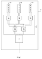
- Fig 1 is a schematic diagram illustrating an environment for receiving uplink signals in a cellular network, where embodiments presented herein can be applied.
- Three antennas 7a-c receive radio signals in the uplink from wireless terminals and provide the received signals to respective filter apparatuses 1a-c.
- Each antenna 7a-c comprises one or more antenna elements, where each antenna element can optionally comprise two sections for receiving two polarisations of signals.
- Each antenna 7a-c can optionally be a MIMO (Multiple Input Multiple Output) antenna, in this case requiring a plurality of antenna elements in each antenna.
- All three antennas 7a-c are associated with a single radio base station 5.
- the three antennas 7a-c can cover a respective sector for the radio base station 5.
- three antennas 7a-c are shown.
- any other umber of antennas can be provided, e.g. one, two, four, etc.
- each one of the filter apparatuses 1a-c filters a part of the input signal and shifts the filtered signal to a new frequency band.
- combiner devices 2a-b can combine the filtered signal into a single multiplexed signal.
- two combiner devices 2a-b are shown, e.g. for each polarisation direction of the antenna elements of the antennas 7a-c.
- any number of combiner devices can be provided, e.g. one, two, three, etc.
- the output of each combiner device can be provided to the radio base station 5 using a single connection over a single cable, using e.g. a single optical fibre or a single galvanic connection.
- the radio base station 5 subsequently demultiplexes the signal components originating from the three antennas 7a-c and performs further uplink processing.
- a controller 8 configures the filter apparatuses 1a-c to provide output signals which do not overlap and can thus be combined and multiplexed on a single cable.
- the controller provides corresponding information to the radio base station 5 such that the radio base station 5 is able to demultiplex and separate the individual signals on the single cable.
- the controller 8 can be provided at the site of the radio base station 5 and filter apparatuses la-c or it can be provided remotely, as long as there is a signalling connection available between the controller 8 and the filter apparatuses 1a-c and the radio base station 5.
- the controller 8 can e.g. for part of a general purpose computer with a user interface allowing an operator to configure how the multiplexing is to occur.
- the radio base station 5 is of any suitable type and can also be called an evolved Node Bs, also known as eNode Bs or eNBs.
- the radio base station 5 could also be in the form of Node Bs, BTSs (Base Transceiver Stations) and/or BSSs (Base Station Subsystems), etc. or any other suitable base station for any current or future mobile communication standard.
- the components shown in Fig 1 are part of a cellular network and may e.g. comply with any one or a combination of LTE-SAE (Long Term Evolution - System Architecture Evolution), W-CDMA (Wideband Code Division Multiplex), EDGE (Enhanced Data Rates for GSM (Global System for Mobile communication) Evolution), GPRS (General Packet Radio Service), CDMA2000 (Code Division Multiple Access 2000), WiMAX (Worldwide Interoperability for Microwave Access) or any other current or future wireless network, such as LTE-Advanced, as long as the principles described hereinafter are applicable.
- LTE-SAE Long Term Evolution - System Architecture Evolution
- W-CDMA Wideband Code Division Multiplex
- EDGE Enhanced Data Rates for GSM (Global System for Mobile communication) Evolution
- GPRS General Packet Radio Service
- CDMA2000 Code Division Multiple Access 2000
- WiMAX Worldwide Interoperability for Microwave Access
- the filter apparatuses 1a-c along with the combiners 2a-b are collectively denoted a multiplex device 9.
- the antennas 7a-c, the filter apparatuses 1a-c, the combiners 2a-b and the radio base station 5 are, in combination, here denoted a radio base station assembly 4.
- a radio base station assembly 4 By multiplexing the signals over the single connection, a lot of energy is saved in the radio base station assembly 4. It has been shown that up to 40% of the energy usage can be saved in this way.
- Fig 2A-C are schematic graphs illustrating how three signals 17a-c can be multiplexed using frequency shifts using the frequency apparatuses 1a-c of Fig 1 .
- three signals 17a-c are shown as received, e.g. by the respective antennas 7a-c of Fig 1 .
- the first signal 17a is received by the first antenna 7a
- the second antenna is received by the second antenna 7b
- the third signal is received by the third antenna.
- the desired signal of all three signals 17a-c is in a particular signal frequency band 12.
- the three signals 17a-c thus comprise a respective desired signal 10a-c, in the frequency band of interest.
- the filter apparatuses 1a-c of Fig 1 comes in.
- the unwanted lower and upper frequency components 18a-c, 19a-c are filtered out.
- the filter apparatuses 1a-c shift the frequency of the desired signals 10a-c so that these could be frequency division multiplexed on a single cable.
- the first desired signal 10a is then a filtered signal which has been shifted to a first frequency band 13a
- the second desired signal 10b is a filtered signal which has been shifted to a second frequency band 13b
- the third desired signal 10c is a filtered signal which has been shifted to a third frequency band 13c.
- one of the three frequency bands 13a-c coincides with the signal frequency band 12.
- the shifting of the desired signals 10a-c is optionally performed such that there are guard bands 16a-b between the respective desired signals. This reduces the risk of interference between the different desired signals 10a-c.
- Figs 2B-B several desired signals can be multiplexed on a single cable.
- the bandwidth and centre frequency for the frequency bands 13a-c of respective desired signals 10a-c can be configured using, e.g. using frequencies of local oscillators of the filter apparatuses described in detail with reference to Figs 3-6 below.
- Each filter apparatus is then provided with its own configuration, such that the frequency bands 13a-c of the desired signals 10a-c do not overlap.
- the frequencies of the oscillators can e.g. be configured using configuration files provided from the controller (8 of Fig 1 ) to the filter apparatuses (1a-c of Fig 1 ) for multiplexing.
- a corresponding configuration file is then provided to the radio base station (5 of Fig 1 ) for demultiplexing.
- the configuration file can e.g. have, for each filter apparatus, a centre frequency of the desired signal as received from the antennas, a bandwidth of the desired signal and a centre frequency of the output signal from the filter apparatus.
- Each filter apparatus can be configured individually by the controller with its own configuration file.
- a common configuration file is provided with identifiers for which filter apparatus a particular configuration is to be applied.
- the common configuration file is an efficient way of configuring the filter apparatuses.
- This configuration of bandwidth and centre frequencies can e.g. be used to configure the guard bands 16a-b of Fig 2C .
- Fig 3 is a schematic diagram illustrating a filter apparatus 1 of Fig 1 .
- the filter apparatus 1 represents any one of the filter apparatuses 1a-c of Fig 1 .
- the frequency apparatus 1 comprises a first amplifier 20a, a first frequency shifter 21a, a first filter 22a, a second frequency shifter 21b, a second amplifier 20b, a second filter 22b and a third frequency shifter 21c connected serially in the mentioned order between an input 30 and an output 31 of the filter apparatus 1.
- the placement of the amplifiers 20a-b can be varied.
- the first amplifier 20a is instead located between the first filter 22a and the second frequency shifter 21b and the second amplifier 20b is instead located between the second filter 22b and the third frequency shifter 21c, which, in at least some cases, reduces noise.
- the amplifiers 20a-b are optional but can be provided to ensure appropriate gain of the signal through the filter apparatus, e.g. to compensate for signal loss through the frequency shifters and filters.
- Three separate shift input signals 25a-c are respectively provided to the three frequency shifters 21a-c.
- the shift input signals 25a-c can e.g. be provided using respective local oscillators 24a-c.
- the frequencies of the local oscillators are calculated from the conditions given by the configuration provided from the controller (8 of Fig 1 ). See Fig 5 below regarding the relationship between the local oscillator frequencies and the input and output centre frequencies and output bandwidth.
- the frequency shifters 21a-c can e.g. be provided using frequency mixers, heterodynes or superheterodynes.
- the frequency shifters 21a-c shift the input signal by combining the input signal with the shift input signal.
- one of the filters 22a-b blocks frequencies below a lower cut-off frequency and the other blocks frequencies above an upper cut-off frequency.
- the filters 22a-b can be provided using any of the following combinations:
- the first filter 22a can be a low-pass filter and the second filter 22b can be a high-pass filter.
- the first filter 22a can be a high-pass filter and the second filter 22b can be a low-pass filter.
- the first filter 22a can be a low-pass filter and the second filter 22b can be a band-pass filter.
- the first filter 22a can be a band-pass filter and the second filter 22b can be a high-pass filter.
- the first filter 22a can be a high-pass filter and the second filter 22b can be a band-pass filter.
- the first filter 22a can be a band-pass filter and the second filter 22b can be a low-pass filter.
- the first filter 22a can be a band-pass filter and the second filter 22b can be a band-pass filter.
- Fig 4 is a schematic diagram illustrating a filter apparatus 1 of Fig 1 according to one embodiment.
- This filter apparatus 1 is similar to the filter apparatus of Fig 3 and the description with reference to Fig 4 will focus on the differences compared to the filter apparatus of Fig 3 .
- This section 30 comprises a fourth amplifier 20d, a fourth frequency shifter 21d, an optional third filter 22c and a fourth local oscillator 24d.
- the fourth local oscillator 24d provides a fourth shift input signal 25d to the fourth frequency shifter 21d.
- the third filter 22c is optionally provided after the fourth frequency shifter 21d. This third filter 22c could e.g. suppress undesired mixing products resulting from the first frequency shifter 21a.
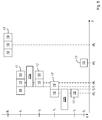
- Fig 5 is a schematic diagram illustrating the operation of the filter apparatus of Figs 1 and 3 . Fig 5 will now be described with further reference to the filter apparatus 1 and its components shown in Fig 3 .
- the vertical axis represents time, where time increases lower down in the figure.
- the horizontal axis represents frequency, where frequency increases to the right in the figure.
- the signal 17 is received on the input 30 of the filter apparatus 1.
- the signal 17 consists of an unwanted lower frequency component 18, a desired signal 10 and an unwanted higher frequency component 19. While the lower and higher frequency components 18-19 here are shown as delimited on the outer ends (away from the desired signal 10), this may or may not be the case.
- the unwanted lower and higher frequency components 18-19 are simply any signal component below or above, respectively, in frequency from the frequency band carrying the desired signal 10.
- the first frequency shifter 21a shifts the signal 17 such that centre frequency of the desired signal 10 is shifted from a first centre frequency cfo to a second centre frequency cf1. Hence, at time t1, the desired signal 10 is situated around the second centre frequency cf1.
- the first filter 22a here illustrated by the frequency band it passes (i.e. not blocks), blocks out the unwanted lower frequency component 18, such that at a time t2, the signal now consists of the desired signal 10 and the unwanted higher frequency component 19.
- the first filter 22a blocks frequencies below a lower cut-off frequency f1, to thereby essentially block out the lower frequency component 18.
- the first filter 22a can here e.g. be a high-pass filter or a band-pass filter.
- the second frequency shifter 21b then shifts the signal 17 such that centre frequency of the desired signal 10 is shifted from the second centre frequency cf1 to a third centre frequency cf2. Hence, at time t3, the desired signal 10 is situated around the third centre frequency cf2.
- the second filter 22b here illustrated by the frequency band it passes (i.e. not blocks), now blocks out the unwanted higher frequency component 19, such that at a time t4, the signal now only essentially consists of the desired signal 10.
- the second filter 22b blocks frequencies above an upper cut-off frequency f2, to thereby essentially block out the higher frequency component 19.
- the second filter 22b can here e.g. be a low-pass filter or a band-pass filter. This second filter also blocks overtones to any generated signals (such as from local oscillators) which have a frequency over the upper cut-off frequency f2.
- the third frequency shifter 21c then shifts the signal 17 such that centre frequency of the desired signal 10 is shifted from the third centre frequency cf2 to a fourth centre frequency cf3.
- the desired signal 10 is situated around the fourth centre frequency cf3.
- the signal 17 is the output signal and can e.g. be provided to a combiner for frequency division multiplexing.
- the fourth centre frequency cf3 is different for different filter apparatuses of the same radio base station assembly, to allow frequency division multiplexing of several signals.
- the unwanted lower and higher frequency components are filtered out, and the resulting signal is provided around the third centre frequency cf3.
- the frequency band of the desired frequency 10 (as extracted from the input signal) and its bandwidth can be configured by only adjusting the first and second shift input signals 25a-b, e.g. using the local oscillators 24a-b.
- the resulting (third) centre frequency cf3 can also be easily configured, by only adjusting the third shift input signal 25c, e.g. using the local oscillator 24c.
- the filters 22a-b can be fixed in frequency characteristics and do not need to be reconfigured in any way for various pass bands or output centre frequencies.
- no switches are required to connect and/or disconnect filters depending on configuration.
- Fig 5 is presented with various discrete points in time, it is to be understood that the filter apparatus 1 does not need to provide certain characteristics at particular points in time; rather, the components of the filter apparatus 1 are connected in a certain way and process signals sequentially as they are provided on the respective component inputs. The points in time of Fig 5 are provided only to more clearly explain how the filter apparatus 1 operates.
- Fig 6 is a schematic diagram illustrating the operation of the filter apparatus of Figs 1 and 4 .
- Fig 6 will now be described with further reference to the filter apparatus 1 and its components shown in Fig 4 .
- Tthe vertical axis represents time, where time increases lower down in the figure.
- the horizontal axis represents frequency, where frequency increases to the right in the figure.
- the operation illustrated in Fig 6 is similar to the operation illustrated in Fig 5 .
- the signal 17 is received on the input 30 of the filter apparatus 1.
- the signal 17 consists of an unwanted lower frequency component 18, a desired signal 10 and an unwanted higher frequency component 19. While the lower and higher frequency components 18-19 here are shown as delimited on the outer ends (away from the desired signal 10), this may or may not be the case.
- the unwanted lower and higher frequency components 18-19 are simply any signal component below or above, respectively, in frequency from the frequency band carrying the desired signal 10.
- the first frequency shifter 21a shifts the signal 17 such that centre frequency of the desired signal 10 is shifted from a first centre frequency cfo to a second centre frequency cf1. Hence, at time t1, the desired signal 10 is situated around the second centre frequency cf1.
- the first filter 22a here illustrated by the frequency band it passes (i.e. not blocks), blocks out the unwanted lower frequency component 18, such that at a time t2, the signal now consists of the desired signal 10 and the unwanted higher frequency component 19.
- the first filter 22a blocks frequencies below a lower cut-off frequency f1, to thereby essentially block out the lower frequency component 18.
- the first filter 22a can here e.g. be a high-pass filter or a band-pass filter.
- the fourth frequency shifter 21d then shifts the signal 17 such that centre frequency of the desired signal 10 is shifted from the second centre frequency cf1 back to the first centre frequency cfo. Hence, at time t2', the desired signal 10 is situated around the third centre frequency cfo.
- the fourth frequency shifter can shift the signal to any other suitable centre frequency, at a significant distance from the second centre frequency cf1.
- the second frequency shifter 21b then shifts the signal 17 such that centre frequency of the desired signal 10 is shifted from the first centre frequency cfo to a third centre frequency cf2. Hence, at time t3, the desired signal 10 is situated around the third centre frequency cf2.
- the second filter 22b here illustrated by the frequency band it passes (i.e. not blocks), now blocks out the unwanted higher frequency component 19, such that at a time t4, the signal now only essentially consists of the desired signal 10.
- the second filter 22b blocks frequencies above an upper cut-off frequency f2, to thereby essentially block out the higher frequency component 19.
- the second filter 22b can here e.g. be a low-pass filter or a band-pass filter. This second filter also blocks overtones to any generated signals (such as from local oscillators) which have a frequency over the upper cut-off frequency f2.
- the third frequency shifter 21c then shifts the signal 17 such that centre frequency of the desired signal 10 is shifted from the third centre frequency cf2 to a fourth centre frequency cf3.
- the desired signal 10 is situated around the fourth centre frequency cf3.
- the signal 17 is the output signal and can e.g. be provided to a combiner for frequency division multiplexing.
- the fourth centre frequency cf3 is different for different filter apparatuses of the same radio base station assembly, to allow frequency division multiplexing of several signals.
- the lower cut-off frequency f1 and the upper cut-off frequency f2 can be the same for the two filters 22a-b.
- this embodiment allows the two filters 22a and 22b to be of the same specification.
- the two filters 22a and 22b can be band pass filters of the same specification.
- Fig 7 is a flow chart illustrating a method 49 performed in the filter apparatus of Figs 1 , 3 and 4 . The method corresponds to the procedure presented with reference to Figs 3 , 4 and 5 .
- a first frequency shift step 40 the signal is frequency shifted using a first frequency shifter. This corresponds to the actions performed between times to and t1 in Fig 5 and Fig 6 .
- a firstfilter step 42 the signal is filtered using a first filter. This corresponds to the actions performed between times t1 and t2 in Fig 5 and Fig 6 .
- a second frequency shift step 44 the signal is frequency shifted using a second frequency shifter. This corresponds to the actions performed between times t2 and t3 in Fig 5 and Fig 6 .
- this step comprises shifting to a significantly higher frequency and shifting to frequency which is lower than the significantly higher frequency. As explained with reference to Fig 6 above, this allows the two filters to be of the same specification.
- a second filter step 46 the signal is filtered using a second filter. This corresponds to the actions performed between times t3 and t4 in Fig 5 and Fig 6 .
- a third frequency shift step 48 the signal is frequency shifted using the third frequency shifter, the output of which is connected to the output of the apparatus. This corresponds to the actions performed between times t4 and t5 in Fig 5 and Fig 6 .
- Fig 9 is a flow chart illustrating a method performed in the multiplex device 9 of Fig 1 . The method is performed to multiplex signals.
- a filter first signal step 49a the filtering method of Fig 7 is performed in the first filter apparatus 1a, which results in a filtered signal of a desired signal from a first source.
- a filter second signal step 49b the filtering method of Fig 7 is performed in the first filter apparatus 1a, which results in a filtered signal of a desired signal from a second source.
- the filter first signal step 49a and the filter second signal step 49b are performed in parallel.
- a combine step 50 the filtered signals from the filter first signal and filter second signal (and filter third signal, etc., if present) steps 49a-b are combined to a combined output.
- filter apparatus While the filter apparatus presented herein is shown as filtering an uplink signal for subsequent frequency division multiplex, the filter apparatus can be used in any appropriate situation, effectively providing a configurable pass-band filter and a configurable frequency shift.
Landscapes
- Engineering & Computer Science (AREA)
- Computer Networks & Wireless Communication (AREA)
- Signal Processing (AREA)
- Physics & Mathematics (AREA)
- Electromagnetism (AREA)
- Power Engineering (AREA)
- Noise Elimination (AREA)
Description
- The invention relates to a multiplex device and associated method.
- In the analogue domain of cellular networks, filtering of various types is often required: prior art examples are disclosed by
US2011/0136443 andWO98/36501 - For example, in the uplink part of some radio base stations, certain frequency sub bands are filtered out and shifted to new centre frequencies. This allows frequency domain multiplexing to reduce the number of cables required between antennas and the main part of the radio base station.
- The frequency band varies in extent and position depending on radio technology used and/or allocations of frequencies for a particular operator. It would be beneficial if there were a filter apparatus which is configurable both in bandwidth of the desired signal and centre frequency for the output signal.
US-5,987,304 presents a mobile telephone repeater with a variable bandwidth. The repeater comprises an uplink and downlink, each being provided with amplifier chains. Each chain comprises at least two band pass filter units coupled in series and having controllable pass bands, which at least partially overlap each other. The center frequency of the filter units are controllable so as to make the bandwidth of the resulting pass band variable. Consequently, the effective bandwidth of the amplifier chain is controllable. However, it would be beneficial if greater flexibility in configuration is achieved, preferably also with fewer components. - It is an object to provide a multiplex device, according to
claim 1, and a method for multiplexing signals, according toclaim 10. - Generally, all terms used in the claims are to be interpreted according to their ordinary meaning in the technical field, unless explicitly defined otherwise herein. All references to "a/an/the element, apparatus, component, means, step, etc." are to be interpreted openly as referring to at least one instance of the element, apparatus, component, means, step, etc., unless explicitly stated otherwise. The steps of any method disclosed herein do not have to be performed in the exact order disclosed, unless explicitly stated.
- The invention is now described, by way of example, with reference to the accompanying drawings, in which:
-
Fig 1 is a schematic diagram illustrating an environment for receiving uplink signals, where embodiments presented herein can be applied; -
Figs 2A-C are schematic graphs illustrating how signals can be multiplexed using frequency shifts using the frequency apparatuses ofFig 1 ; -
Fig 3 is a schematic diagram illustrating a filter apparatus ofFig 1 according to one embodiment; -
Fig 4 is a schematic diagram illustrating a filter apparatus ofFig 1 according to one embodiment; -
Fig 5 is a schematic diagram illustrating the operation of the filter apparatus ofFigs 1 and3 ; -
Fig 6 is a schematic diagram illustrating the operation of the filter apparatus ofFig 1 and4 ; -
Fig 7 is a flow chart illustrating a method performed in the filter apparatus ofFigs 1 ,3 and4 , and -
Fig 8 is a flow chart illustrating a method performed in the multiplex device ofFig 1 . - The invention will now be described more fully hereinafter with reference to the accompanying drawings, in which certain embodiments of the invention are shown. This invention may, however, be embodied in many different forms and should not be construed as limited to the embodiments set forth herein; rather, these embodiments are provided by way of example so that this disclosure will be thorough and complete, and will fully convey the scope of the invention to those skilled in the art. Like numbers refer to like elements throughout the description.
-
Fig 1 is a schematic diagram illustrating an environment for receiving uplink signals in a cellular network, where embodiments presented herein can be applied. Threeantennas 7a-c receive radio signals in the uplink from wireless terminals and provide the received signals torespective filter apparatuses 1a-c. Eachantenna 7a-c comprises one or more antenna elements, where each antenna element can optionally comprise two sections for receiving two polarisations of signals. Eachantenna 7a-c can optionally be a MIMO (Multiple Input Multiple Output) antenna, in this case requiring a plurality of antenna elements in each antenna. All threeantennas 7a-c are associated with a singleradio base station 5. For example, the threeantennas 7a-c can cover a respective sector for theradio base station 5. In the example shown inFig 1 , threeantennas 7a-c are shown. However, any other umber of antennas can be provided, e.g. one, two, four, etc. - As is explained in more detail below, each one of the
filter apparatuses 1a-c filters a part of the input signal and shifts the filtered signal to a new frequency band. In this way, combinerdevices 2a-b can combine the filtered signal into a single multiplexed signal. In the example illustrated inFig 1 , twocombiner devices 2a-b are shown, e.g. for each polarisation direction of the antenna elements of theantennas 7a-c. However, any number of combiner devices can be provided, e.g. one, two, three, etc. In any case, by combining the components from thefilter apparatuses 1a-c, the output of each combiner device can be provided to theradio base station 5 using a single connection over a single cable, using e.g. a single optical fibre or a single galvanic connection. Theradio base station 5 subsequently demultiplexes the signal components originating from the threeantennas 7a-c and performs further uplink processing. - A controller 8 configures the
filter apparatuses 1a-c to provide output signals which do not overlap and can thus be combined and multiplexed on a single cable. The controller provides corresponding information to theradio base station 5 such that theradio base station 5 is able to demultiplex and separate the individual signals on the single cable. The controller 8 can be provided at the site of theradio base station 5 and filter apparatuses la-c or it can be provided remotely, as long as there is a signalling connection available between the controller 8 and thefilter apparatuses 1a-c and theradio base station 5. The controller 8 can e.g. for part of a general purpose computer with a user interface allowing an operator to configure how the multiplexing is to occur. - The
radio base station 5 is of any suitable type and can also be called an evolved Node Bs, also known as eNode Bs or eNBs. Theradio base station 5 could also be in the form of Node Bs, BTSs (Base Transceiver Stations) and/or BSSs (Base Station Subsystems), etc. or any other suitable base station for any current or future mobile communication standard. - The components shown in
Fig 1 are part of a cellular network and may e.g. comply with any one or a combination of LTE-SAE (Long Term Evolution - System Architecture Evolution), W-CDMA (Wideband Code Division Multiplex), EDGE (Enhanced Data Rates for GSM (Global System for Mobile communication) Evolution), GPRS (General Packet Radio Service), CDMA2000 (Code Division Multiple Access 2000), WiMAX (Worldwide Interoperability for Microwave Access) or any other current or future wireless network, such as LTE-Advanced, as long as the principles described hereinafter are applicable. - The
filter apparatuses 1a-c along with thecombiners 2a-b are collectively denoted amultiplex device 9. - The
antennas 7a-c, thefilter apparatuses 1a-c, thecombiners 2a-b and theradio base station 5 are, in combination, here denoted a radiobase station assembly 4. By multiplexing the signals over the single connection, a lot of energy is saved in the radiobase station assembly 4. It has been shown that up to 40% of the energy usage can be saved in this way. -
Fig 2A-C are schematic graphs illustrating how threesignals 17a-c can be multiplexed using frequency shifts using thefrequency apparatuses 1a-c ofFig 1 . InFig 2A , threesignals 17a-c are shown as received, e.g. by therespective antennas 7a-c ofFig 1 . In other words, thefirst signal 17a is received by thefirst antenna 7a, the second antenna is received by thesecond antenna 7b and the third signal is received by the third antenna. The desired signal of all threesignals 17a-c is in a particularsignal frequency band 12. The threesignals 17a-c thus comprise a respective desiredsignal 10a-c, in the frequency band of interest. It can be seen fromfig 2A that three desiredsignals 10a-c can not directly be frequency division multiplexed since the three desiredsignals 10a-c all occupy the samesignal frequency band 12. Furthermore, for each desiredsignal 10a-c, there are a respective unwantedlower frequency component 18a-c and a respective unwantedhigher frequency component 19a-c. - This is where the
filter apparatuses 1a-c ofFig 1 comes in. Using therespective filter apparatuses 1a-c for the respective signals, the unwanted lower andupper frequency components 18a-c, 19a-c are filtered out. Moreover, as seen inFig 2B , thefilter apparatuses 1a-c shift the frequency of the desiredsignals 10a-c so that these could be frequency division multiplexed on a single cable. For example, the first desiredsignal 10a is then a filtered signal which has been shifted to afirst frequency band 13a, the second desiredsignal 10b is a filtered signal which has been shifted to asecond frequency band 13b and the third desiredsignal 10c is a filtered signal which has been shifted to athird frequency band 13c. Optionally, one of the threefrequency bands 13a-c coincides with thesignal frequency band 12. - As can be seen in
Fig 2C , the shifting of the desiredsignals 10a-c is optionally performed such that there areguard bands 16a-b between the respective desired signals. This reduces the risk of interference between the different desiredsignals 10a-c. - As can be seen in
Figs 2B-B , several desired signals can be multiplexed on a single cable. This gives a possibility to optimise utilisation of available bandwidth over the single cable. The bandwidth and centre frequency for thefrequency bands 13a-c of respective desiredsignals 10a-c can be configured using, e.g. using frequencies of local oscillators of the filter apparatuses described in detail with reference toFigs 3-6 below. Each filter apparatus is then provided with its own configuration, such that thefrequency bands 13a-c of the desiredsignals 10a-c do not overlap. The frequencies of the oscillators can e.g. be configured using configuration files provided from the controller (8 ofFig 1 ) to the filter apparatuses (1a-c ofFig 1 ) for multiplexing. A corresponding configuration file is then provided to the radio base station (5 ofFig 1 ) for demultiplexing. - The configuration file can e.g. have, for each filter apparatus, a centre frequency of the desired signal as received from the antennas, a bandwidth of the desired signal and a centre frequency of the output signal from the filter apparatus. Each filter apparatus can be configured individually by the controller with its own configuration file. Alternatively, a common configuration file is provided with identifiers for which filter apparatus a particular configuration is to be applied. The common configuration file is an efficient way of configuring the filter apparatuses.
- This configuration of bandwidth and centre frequencies can e.g. be used to configure the
guard bands 16a-b ofFig 2C . -
Fig 3 is a schematic diagram illustrating afilter apparatus 1 ofFig 1 . Thefilter apparatus 1 represents any one of thefilter apparatuses 1a-c ofFig 1 . Thefrequency apparatus 1 comprises afirst amplifier 20a, afirst frequency shifter 21a, afirst filter 22a, asecond frequency shifter 21b, asecond amplifier 20b, asecond filter 22b and athird frequency shifter 21c connected serially in the mentioned order between aninput 30 and anoutput 31 of thefilter apparatus 1. The placement of theamplifiers 20a-b can be varied. In one embodiment, thefirst amplifier 20a is instead located between thefirst filter 22a and thesecond frequency shifter 21b and thesecond amplifier 20b is instead located between thesecond filter 22b and thethird frequency shifter 21c, which, in at least some cases, reduces noise. - The
amplifiers 20a-b are optional but can be provided to ensure appropriate gain of the signal through the filter apparatus, e.g. to compensate for signal loss through the frequency shifters and filters. - Three separate shift input signals 25a-c are respectively provided to the three
frequency shifters 21a-c. The shift input signals 25a-c can e.g. be provided using respectivelocal oscillators 24a-c. The frequencies of the local oscillators are calculated from the conditions given by the configuration provided from the controller (8 ofFig 1 ). SeeFig 5 below regarding the relationship between the local oscillator frequencies and the input and output centre frequencies and output bandwidth. - The
frequency shifters 21a-c can e.g. be provided using frequency mixers, heterodynes or superheterodynes. Thefrequency shifters 21a-c shift the input signal by combining the input signal with the shift input signal. - As will be explained in more detail below, one of the
filters 22a-b blocks frequencies below a lower cut-off frequency and the other blocks frequencies above an upper cut-off frequency. So for example, thefilters 22a-b can be provided using any of the following combinations: Thefirst filter 22a can be a low-pass filter and thesecond filter 22b can be a high-pass filter. Thefirst filter 22a can be a high-pass filter and thesecond filter 22b can be a low-pass filter. Thefirst filter 22a can be a low-pass filter and thesecond filter 22b can be a band-pass filter. Thefirst filter 22a can be a band-pass filter and thesecond filter 22b can be a high-pass filter. Thefirst filter 22a can be a high-pass filter and thesecond filter 22b can be a band-pass filter. Thefirst filter 22a can be a band-pass filter and thesecond filter 22b can be a low-pass filter. Thefirst filter 22a can be a band-pass filter and thesecond filter 22b can be a band-pass filter. -
Fig 4 is a schematic diagram illustrating afilter apparatus 1 ofFig 1 according to one embodiment. Thisfilter apparatus 1 is similar to the filter apparatus ofFig 3 and the description with reference toFig 4 will focus on the differences compared to the filter apparatus ofFig 3 . In this embodiment, there is asection 30 of additional components between thefirst filter 22a and thesecond frequency shifter 21b. Thissection 30 comprises afourth amplifier 20d, afourth frequency shifter 21d, an optionalthird filter 22c and a fourthlocal oscillator 24d. The fourthlocal oscillator 24d provides a fourthshift input signal 25d to thefourth frequency shifter 21d. As is explained below with reference toFig 6 , this makes is possible for the first andsecond filters - The
third filter 22c is optionally provided after thefourth frequency shifter 21d. Thisthird filter 22c could e.g. suppress undesired mixing products resulting from thefirst frequency shifter 21a. -
Fig 5 is a schematic diagram illustrating the operation of the filter apparatus ofFigs 1 and3 .Fig 5 will now be described with further reference to thefilter apparatus 1 and its components shown inFig 3 . - The vertical axis represents time, where time increases lower down in the figure. The horizontal axis represents frequency, where frequency increases to the right in the figure.
- At time to, the
signal 17 is received on theinput 30 of thefilter apparatus 1. Thesignal 17 consists of an unwantedlower frequency component 18, a desiredsignal 10 and an unwantedhigher frequency component 19. While the lower and higher frequency components 18-19 here are shown as delimited on the outer ends (away from the desired signal 10), this may or may not be the case. The unwanted lower and higher frequency components 18-19 are simply any signal component below or above, respectively, in frequency from the frequency band carrying the desiredsignal 10. - The
first frequency shifter 21a shifts thesignal 17 such that centre frequency of the desiredsignal 10 is shifted from a first centre frequency cfo to a second centre frequency cf1. Hence, at time t1, the desiredsignal 10 is situated around the second centre frequency cf1. - The
first filter 22a, here illustrated by the frequency band it passes (i.e. not blocks), blocks out the unwantedlower frequency component 18, such that at a time t2, the signal now consists of the desiredsignal 10 and the unwantedhigher frequency component 19. Thefirst filter 22a blocks frequencies below a lower cut-off frequency f1, to thereby essentially block out thelower frequency component 18. Hence, thefirst filter 22a can here e.g. be a high-pass filter or a band-pass filter. - The
second frequency shifter 21b then shifts thesignal 17 such that centre frequency of the desiredsignal 10 is shifted from the second centre frequency cf1 to a third centre frequency cf2. Hence, at time t3, the desiredsignal 10 is situated around the third centre frequency cf2. - The
second filter 22b, here illustrated by the frequency band it passes (i.e. not blocks), now blocks out the unwantedhigher frequency component 19, such that at a time t4, the signal now only essentially consists of the desiredsignal 10. Thesecond filter 22b blocks frequencies above an upper cut-off frequency f2, to thereby essentially block out thehigher frequency component 19. Hence, thesecond filter 22b can here e.g. be a low-pass filter or a band-pass filter. This second filter also blocks overtones to any generated signals (such as from local oscillators) which have a frequency over the upper cut-off frequency f2. - The
third frequency shifter 21c then shifts thesignal 17 such that centre frequency of the desiredsignal 10 is shifted from the third centre frequency cf2 to a fourth centre frequency cf3. Hence, at time t5, the desiredsignal 10 is situated around the fourth centre frequency cf3. At this time t5, thesignal 17 is the output signal and can e.g. be provided to a combiner for frequency division multiplexing. The fourth centre frequency cf3 is different for different filter apparatuses of the same radio base station assembly, to allow frequency division multiplexing of several signals. - Through the provided filter apparatus, the unwanted lower and higher frequency components are filtered out, and the resulting signal is provided around the third centre frequency cf3. This is achieved by the low component count and cost effective structure provided for the
filter apparatus 1. Moreover, the frequency band of the desired frequency 10 (as extracted from the input signal) and its bandwidth can be configured by only adjusting the first and second shift input signals 25a-b, e.g. using thelocal oscillators 24a-b. Also, the resulting (third) centre frequency cf3 can also be easily configured, by only adjusting the thirdshift input signal 25c, e.g. using thelocal oscillator 24c. In other words, thefilters 22a-b can be fixed in frequency characteristics and do not need to be reconfigured in any way for various pass bands or output centre frequencies. Moreover, no switches are required to connect and/or disconnect filters depending on configuration. - While
Fig 5 is presented with various discrete points in time, it is to be understood that thefilter apparatus 1 does not need to provide certain characteristics at particular points in time; rather, the components of thefilter apparatus 1 are connected in a certain way and process signals sequentially as they are provided on the respective component inputs. The points in time ofFig 5 are provided only to more clearly explain how thefilter apparatus 1 operates. - It is to be noted that while the procedure illustrated in
Fig 5 first blocks out the unwantedlower frequency component 18 and secondly blocks out the unwantedhigher frequency component 19, the procedure can equally well be changed such that it first blocks out the unwantedhigher frequency component 19 and secondly blocks out the unwantedlower frequency component 18, -
Fig 6 is a schematic diagram illustrating the operation of the filter apparatus ofFigs 1 and4 .Fig 6 will now be described with further reference to thefilter apparatus 1 and its components shown inFig 4 . Tthe vertical axis represents time, where time increases lower down in the figure. The horizontal axis represents frequency, where frequency increases to the right in the figure. The operation illustrated inFig 6 is similar to the operation illustrated inFig 5 . - At time to, the
signal 17 is received on theinput 30 of thefilter apparatus 1. Thesignal 17 consists of an unwantedlower frequency component 18, a desiredsignal 10 and an unwantedhigher frequency component 19. While the lower and higher frequency components 18-19 here are shown as delimited on the outer ends (away from the desired signal 10), this may or may not be the case. The unwanted lower and higher frequency components 18-19 are simply any signal component below or above, respectively, in frequency from the frequency band carrying the desiredsignal 10. - The
first frequency shifter 21a shifts thesignal 17 such that centre frequency of the desiredsignal 10 is shifted from a first centre frequency cfo to a second centre frequency cf1. Hence, at time t1, the desiredsignal 10 is situated around the second centre frequency cf1. - The
first filter 22a, here illustrated by the frequency band it passes (i.e. not blocks), blocks out the unwantedlower frequency component 18, such that at a time t2, the signal now consists of the desiredsignal 10 and the unwantedhigher frequency component 19. Thefirst filter 22a blocks frequencies below a lower cut-off frequency f1, to thereby essentially block out thelower frequency component 18. Hence, thefirst filter 22a can here e.g. be a high-pass filter or a band-pass filter. - The
fourth frequency shifter 21d then shifts thesignal 17 such that centre frequency of the desiredsignal 10 is shifted from the second centre frequency cf1 back to the first centre frequency cfo. Hence, at time t2', the desiredsignal 10 is situated around the third centre frequency cfo. Optionally, the fourth frequency shifter can shift the signal to any other suitable centre frequency, at a significant distance from the second centre frequency cf1. - The
second frequency shifter 21b then shifts thesignal 17 such that centre frequency of the desiredsignal 10 is shifted from the first centre frequency cfo to a third centre frequency cf2. Hence, at time t3, the desiredsignal 10 is situated around the third centre frequency cf2. - The
second filter 22b, here illustrated by the frequency band it passes (i.e. not blocks), now blocks out the unwantedhigher frequency component 19, such that at a time t4, the signal now only essentially consists of the desiredsignal 10. Thesecond filter 22b blocks frequencies above an upper cut-off frequency f2, to thereby essentially block out thehigher frequency component 19. Hence, thesecond filter 22b can here e.g. be a low-pass filter or a band-pass filter. This second filter also blocks overtones to any generated signals (such as from local oscillators) which have a frequency over the upper cut-off frequency f2. - The
third frequency shifter 21c then shifts thesignal 17 such that centre frequency of the desiredsignal 10 is shifted from the third centre frequency cf2 to a fourth centre frequency cf3. Hence, at time t5, the desiredsignal 10 is situated around the fourth centre frequency cf3. At this time t5, thesignal 17 is the output signal and can e.g. be provided to a combiner for frequency division multiplexing. The fourth centre frequency cf3 is different for different filter apparatuses of the same radio base station assembly, to allow frequency division multiplexing of several signals. - In comparison with the operation illustrated in
Fig 5 , by configuring the local oscillators, the lower cut-off frequency f1 and the upper cut-off frequency f2 can be the same for the twofilters 22a-b. In other words, this embodiment allows the twofilters filters - In theory, between times t2 and t3, the signal could be shifted directly between the second centre frequency cf1 and the third centre frequency cf2. However, when the second centre frequency cf1 and the third centre frequency cf2 are close, by having the middle step of shifting back to a significantly higher centre frequency, mirror frequencies are reduced or even eliminated. Significantly higher can here e.g. be interpreted as at least double.
Fig 7 is a flow chart illustrating amethod 49 performed in the filter apparatus ofFigs 1 ,3 and4 . The method corresponds to the procedure presented with reference toFigs 3 ,4 and5 . - In a first
frequency shift step 40, the signal is frequency shifted using a first frequency shifter. This corresponds to the actions performed between times to and t1 inFig 5 andFig 6 . - In a
firstfilter step 42, the signal is filtered using a first filter. This corresponds to the actions performed between times t1 and t2 inFig 5 andFig 6 . - In a second
frequency shift step 44, the signal is frequency shifted using a second frequency shifter. This corresponds to the actions performed between times t2 and t3 inFig 5 andFig 6 . Optionally, this step comprises shifting to a significantly higher frequency and shifting to frequency which is lower than the significantly higher frequency. As explained with reference toFig 6 above, this allows the two filters to be of the same specification. - In a
second filter step 46, the signal is filtered using a second filter. This corresponds to the actions performed between times t3 and t4 inFig 5 andFig 6 . - In a third
frequency shift step 48, the signal is frequency shifted using the third frequency shifter, the output of which is connected to the output of the apparatus. This corresponds to the actions performed between times t4 and t5 inFig 5 andFig 6 . - Fig 9 is a flow chart illustrating a method performed in the
multiplex device 9 ofFig 1 . The method is performed to multiplex signals. - In a filter
first signal step 49a, the filtering method ofFig 7 is performed in thefirst filter apparatus 1a, which results in a filtered signal of a desired signal from a first source. - In a filter
second signal step 49b, the filtering method ofFig 7 is performed in thefirst filter apparatus 1a, which results in a filtered signal of a desired signal from a second source. - The filter
first signal step 49a and the filtersecond signal step 49b are performed in parallel. Optionally, there is further filter third signal step (not shown) or even more filtering steps, corresponding to the number of filtering apparatuses there are in the multiplex device. - In a
combine step 50, the filtered signals from the filter first signal and filter second signal (and filter third signal, etc., if present) steps 49a-b are combined to a combined output. - While the filter apparatus presented herein is shown as filtering an uplink signal for subsequent frequency division multiplex, the filter apparatus can be used in any appropriate situation, effectively providing a configurable pass-band filter and a configurable frequency shift.
- The invention has mainly been described above with reference to a few embodiments. However, as is readily appreciated by a person skilled in the art, other embodiments than the ones disclosed above are equally possible within the scope of the invention, as defined by the appended patent claims.
Claims (15)
- A multiplex device (9) comprising, at least two filter apparatuses (1, 1a, 1b, 1c) that each comprises,
a first frequency shifter (21a) arranged to accept an input signal of the apparatus;
a first filter (22a) with and input from the first frequency shifter;
a second frequency shifter (21b) arranged to receive the signal from the first filter;
a second filter (22b) with and input from the second frequency shifter; and
a third frequency shifter (21c), with and input from the second filter and the output of which is connected to the output of the apparatus,
wherein one of the first and the second filters blocks frequencies below a lower cut-off frequency, and the other of the first and the second filter blocks frequencies above an upper cut-off frequency;
wherein the first frequency shifter (21a), the first filter (22a), the second frequency shifter (21b), the second filter (22b) and the third frequency shifter (21c) are serially connected;
wherein each one of the first frequency shifter (21a), second frequency shifter (21b) and third frequency shifter (21c) has separate shift input signals (25a-c), respectively;wherein the two filter apparatuses are arranged to provide a respective filtered signal at non-overlapping frequency bands on their outputs, and the bandwidth of the respective filtered signal is configurable by adjustment of the shift input signal to the first frequency shifter (21a) and by adjustment of the shift input signal to the second frequency shifter (21b)a combiner device (2a-b) comprising at least two combiner inputs, respectively connected to the outputs of the at least two filter apparatuses (1a-c), the combiner device further comprising a combiner output for providing an output signal which is a combination of the signals provided on the at least two combiner inputs. - The multiplex device (9) according to claim 1, wherein the output of the first frequency shifter (21a) is connected to the input of the first filter (22a), the output of the first filter (22a) is connected to the input of the second frequency shifter (21b), the output of the second frequency shifter (21b) is connected to the input of the second filter (22b), and the output of the second filter (22b) is connected to the third frequency shifter (21c).
- The multiplex device (9) according to claim 1 or 2, further comprising a fourth frequency shifter (21d) and a third filter (22c), connected serially between the first filter (22a) and the second frequency shifter (21b).
- The multiplex device (9) according to any one of the preceding claims, wherein the first filter (22a) is arranged to block frequencies below a lower cut-off frequency and the second filter (22b) is arranged to block frequencies above an upper cut-off frequency.
- The multiplex device (9) according to any one of the preceding claims, wherein the first filter (22a) is a high-pass filter and the second filter (22b) is a low-pass filter.
- The multiplex device (9) according to any one of claims 1 to 3, wherein the second filter (22b) is arranged to block frequencies below a lower cut-off frequency and the first filter (22a) is arranged to block frequencies above an upper cut-off frequency.
- The multiplex device (9) according to any one of claims 1, 2, 3 and 6, wherein the first filter (22a) is a low-pass filter and the second filter (22b) is a high-pass filter.
- The multiplex device (9) according to any one of the preceding claims, wherein the first filter (22a) is a band-pass filter and the second filter (22b) is a band-pass filter
- The multiplex device (9) according to any preceding claim , comprising two combiner devices (2a-b) for handling two different signals of two different polarisations.
- A method for multiplexing signals, the method being performed in a multiplex device (9) comprising a first filter apparatus (1a), a second filter apparatus (1b) and a combiner device (2a-b), the method comprising performing (49a-b) in the first filter apparatus (1a) and in the second filter apparatus (1b), respectively, the steps of:first frequency shifting (40) the signal using a first frequency shifter (21a) and a first shift input signal (25a);first filtering (42) the signal, after the first frequency shifting, using a first filter (22a);second frequency shifting (44) the signal, after the first filtering, using a second frequency shifter (21b) and a second shift input signal (25b);second filtering (46) the signal, after the second frequency shifting, using a second filter (22b), wherein in one of the first and the second filtering frequencies below a lower cut-off frequency are blocked, and in the other of the first and the second filtering frequencies above an upper cut-off frequency are blocked;third frequency shifting (48) the signal, after the second frequency shifting, using a third frequency shifter (21c) and a third shift input signal (25c), the output of which is connected to the output of the filter apparatus,thereby providing at the output of the first and the second filter apparatus (1a, 1b) filtered signals at non-overlapping frequency bands wherein the bandwidth of the respective filtered signal is configurable by adjustment of the shift input signal to the first frequency shifter (21a) and by adjustment of the shift input signal to the second frequency shifter (21b); and comprising the further step of,combining (50) in the combiner, the filtered signals to a combined output.
- The method according to claim 10, wherein the first filtering step (42) comprises blocking frequencies below a lower cut-off frequency and the second filtering step (46) comprises blocking frequencies above an upper cut-off frequency.
- The method according to claim 10 or 11, wherein the first filter (22a) is a high-pass filter and the second filter (22b) is a low-pass filter.
- The method according to claim 10, wherein the second filtering step (46) comprises blocking frequencies below a lower cut-off frequency and the first filtering step (46) comprises blocking frequencies above an upper cut-off frequency.
- The method according to claim 10 or 13, wherein the first filter (22a) is a low-pass filter and the second filter (22b) is a high-pass filter.
- The method according to any one of claims 10 to 14, wherein the first filter (22a) is a band-pass filter and the second filter (22b) is a band-pass filter.
Applications Claiming Priority (3)
| Application Number | Priority Date | Filing Date | Title |
|---|---|---|---|
| US201261712456P | 2012-10-11 | 2012-10-11 | |
| US201261737346P | 2012-12-14 | 2012-12-14 | |
| PCT/SE2013/050645 WO2014058374A1 (en) | 2012-10-11 | 2013-06-04 | Filter apparatus, multiplex device and associated method |
Publications (2)
| Publication Number | Publication Date |
|---|---|
| EP2907247A1 EP2907247A1 (en) | 2015-08-19 |
| EP2907247B1 true EP2907247B1 (en) | 2016-11-23 |
Family
ID=48700675
Family Applications (1)
| Application Number | Title | Priority Date | Filing Date |
|---|---|---|---|
| EP13732269.9A Active EP2907247B1 (en) | 2012-10-11 | 2013-06-04 | Multiplex device and associated method |
Country Status (3)
| Country | Link |
|---|---|
| US (1) | US9337947B2 (en) |
| EP (1) | EP2907247B1 (en) |
| WO (1) | WO2014058374A1 (en) |
Families Citing this family (1)
| Publication number | Priority date | Publication date | Assignee | Title |
|---|---|---|---|---|
| EP3883247A4 (en) * | 2018-12-13 | 2021-12-01 | Huawei Technologies Co., Ltd. | FILTERING DEVICE AND METHOD |
Family Cites Families (6)
| Publication number | Priority date | Publication date | Assignee | Title |
|---|---|---|---|---|
| SE510569C2 (en) * | 1996-05-31 | 1999-06-07 | Allgon Ab | Variable bandwidth repeater |
| US5881375A (en) * | 1997-01-31 | 1999-03-09 | Glenayre Electronics, Inc. | Paging transmitter having broadband exciter using an intermediate frequency above the transmit frequency |
| JP4380174B2 (en) * | 2003-02-27 | 2009-12-09 | 沖電気工業株式会社 | Band correction device |
| US8254865B2 (en) * | 2006-04-07 | 2012-08-28 | Belair Networks | System and method for frequency offsetting of information communicated in MIMO-based wireless networks |
| GB0615567D0 (en) * | 2006-08-05 | 2006-09-13 | Lime Microsystems Ltd | Broadband wireless transmitter and receiver circuitry |
| US8086197B2 (en) * | 2008-11-12 | 2011-12-27 | Nxp B.V. | Multi-channel receiver architecture and reception method |
-
2013
- 2013-06-04 US US14/003,064 patent/US9337947B2/en not_active Expired - Fee Related
- 2013-06-04 EP EP13732269.9A patent/EP2907247B1/en active Active
- 2013-06-04 WO PCT/SE2013/050645 patent/WO2014058374A1/en not_active Ceased
Non-Patent Citations (1)
| Title |
|---|
| None * |
Also Published As
| Publication number | Publication date |
|---|---|
| EP2907247A1 (en) | 2015-08-19 |
| US9337947B2 (en) | 2016-05-10 |
| WO2014058374A1 (en) | 2014-04-17 |
| US20140105203A1 (en) | 2014-04-17 |
Similar Documents
| Publication | Publication Date | Title |
|---|---|---|
| US10075252B2 (en) | Telecommunication system using multiple Nyquist zone operations | |
| US9356697B2 (en) | Distributed antenna system and method | |
| US10355769B2 (en) | Narrowband signal transport sub-system for distributed antenna system | |
| RU2280335C2 (en) | Transmitting circuit for cell base station | |
| US12224837B2 (en) | Systems and methods for reconfigurable repeaters for wireless telecommunications | |
| KR20110091890A (en) | Frequency-variable Filter Using Digital Filter and Band Stop Filtering | |
| KR20130103732A (en) | Apparatus and method for a multiband radio operating in a wireless network | |
| US8743981B2 (en) | Modulation method and apparatus | |
| CN104219020B (en) | IQ data processing method and system of remote radio unit and remote radio unit | |
| US20090011736A1 (en) | Switching Channel Pass Receive Filter | |
| CN106559110B (en) | Active antenna, carrier aggregation method and system | |
| JP5911811B2 (en) | Method and apparatus for transmitting / receiving electromagnetic signals received / transmitted in one or more first frequency bands | |
| US10560134B2 (en) | Multiband aggregation receiver architecture | |
| US9337947B2 (en) | Filter apparatus, multiplex device and associated method | |
| US9781771B2 (en) | Wireless circuit | |
| CN110224704B (en) | Radio frequency system and base station equipment | |
| JP7556966B2 (en) | Communication Equipment and Network Devices | |
| US8837634B2 (en) | Methods and apparatus for signal filtering | |
| KR101482490B1 (en) | Feeder sharing device and system in mobile communication system | |
| KR20160087171A (en) | Wireless communication integration system for joint use of wireless apparatus | |
| KR101582927B1 (en) | Wireless communication integration device preventing inter-modulation distortion | |
| CN119814057A (en) | Wireless communication device and system | |
| CN105450250A (en) | Filtering device, control method of electronic device, electronic device | |
| WO2021059733A1 (en) | Wireless transmission device | |
| KR20150140255A (en) | Wireless communication integration device preventing inter-modulation distortion |
Legal Events
| Date | Code | Title | Description |
|---|---|---|---|
| PUAI | Public reference made under article 153(3) epc to a published international application that has entered the european phase |
Free format text: ORIGINAL CODE: 0009012 |
|
| 17P | Request for examination filed |
Effective date: 20150416 |
|
| AK | Designated contracting states |
Kind code of ref document: A1 Designated state(s): AL AT BE BG CH CY CZ DE DK EE ES FI FR GB GR HR HU IE IS IT LI LT LU LV MC MK MT NL NO PL PT RO RS SE SI SK SM TR |
|
| AX | Request for extension of the european patent |
Extension state: BA ME |
|
| GRAP | Despatch of communication of intention to grant a patent |
Free format text: ORIGINAL CODE: EPIDOSNIGR1 |
|
| INTG | Intention to grant announced |
Effective date: 20160727 |
|
| GRAS | Grant fee paid |
Free format text: ORIGINAL CODE: EPIDOSNIGR3 |
|
| GRAA | (expected) grant |
Free format text: ORIGINAL CODE: 0009210 |
|
| AK | Designated contracting states |
Kind code of ref document: B1 Designated state(s): AL AT BE BG CH CY CZ DE DK EE ES FI FR GB GR HR HU IE IS IT LI LT LU LV MC MK MT NL NO PL PT RO RS SE SI SK SM TR |
|
| AX | Request for extension of the european patent |
Extension state: BA ME |
|
| REG | Reference to a national code |
Ref country code: GB Ref legal event code: FG4D |
|
| REG | Reference to a national code |
Ref country code: CH Ref legal event code: EP |
|
| REG | Reference to a national code |
Ref country code: IE Ref legal event code: FG4D |
|
| REG | Reference to a national code |
Ref country code: AT Ref legal event code: REF Ref document number: 848726 Country of ref document: AT Kind code of ref document: T Effective date: 20161215 |
|
| REG | Reference to a national code |
Ref country code: DE Ref legal event code: R096 Ref document number: 602013014418 Country of ref document: DE |
|
| PG25 | Lapsed in a contracting state [announced via postgrant information from national office to epo] |
Ref country code: LV Free format text: LAPSE BECAUSE OF FAILURE TO SUBMIT A TRANSLATION OF THE DESCRIPTION OR TO PAY THE FEE WITHIN THE PRESCRIBED TIME-LIMIT Effective date: 20161123 |
|
| REG | Reference to a national code |
Ref country code: LT Ref legal event code: MG4D |
|
| REG | Reference to a national code |
Ref country code: NL Ref legal event code: MP Effective date: 20161123 |
|
| REG | Reference to a national code |
Ref country code: AT Ref legal event code: MK05 Ref document number: 848726 Country of ref document: AT Kind code of ref document: T Effective date: 20161123 |
|
| PG25 | Lapsed in a contracting state [announced via postgrant information from national office to epo] |
Ref country code: NO Free format text: LAPSE BECAUSE OF FAILURE TO SUBMIT A TRANSLATION OF THE DESCRIPTION OR TO PAY THE FEE WITHIN THE PRESCRIBED TIME-LIMIT Effective date: 20170223 Ref country code: GR Free format text: LAPSE BECAUSE OF FAILURE TO SUBMIT A TRANSLATION OF THE DESCRIPTION OR TO PAY THE FEE WITHIN THE PRESCRIBED TIME-LIMIT Effective date: 20170224 Ref country code: SE Free format text: LAPSE BECAUSE OF FAILURE TO SUBMIT A TRANSLATION OF THE DESCRIPTION OR TO PAY THE FEE WITHIN THE PRESCRIBED TIME-LIMIT Effective date: 20161123 Ref country code: NL Free format text: LAPSE BECAUSE OF FAILURE TO SUBMIT A TRANSLATION OF THE DESCRIPTION OR TO PAY THE FEE WITHIN THE PRESCRIBED TIME-LIMIT Effective date: 20161123 Ref country code: LT Free format text: LAPSE BECAUSE OF FAILURE TO SUBMIT A TRANSLATION OF THE DESCRIPTION OR TO PAY THE FEE WITHIN THE PRESCRIBED TIME-LIMIT Effective date: 20161123 |
|
| PG25 | Lapsed in a contracting state [announced via postgrant information from national office to epo] |
Ref country code: FI Free format text: LAPSE BECAUSE OF FAILURE TO SUBMIT A TRANSLATION OF THE DESCRIPTION OR TO PAY THE FEE WITHIN THE PRESCRIBED TIME-LIMIT Effective date: 20161123 Ref country code: PL Free format text: LAPSE BECAUSE OF FAILURE TO SUBMIT A TRANSLATION OF THE DESCRIPTION OR TO PAY THE FEE WITHIN THE PRESCRIBED TIME-LIMIT Effective date: 20161123 Ref country code: ES Free format text: LAPSE BECAUSE OF FAILURE TO SUBMIT A TRANSLATION OF THE DESCRIPTION OR TO PAY THE FEE WITHIN THE PRESCRIBED TIME-LIMIT Effective date: 20161123 Ref country code: PT Free format text: LAPSE BECAUSE OF FAILURE TO SUBMIT A TRANSLATION OF THE DESCRIPTION OR TO PAY THE FEE WITHIN THE PRESCRIBED TIME-LIMIT Effective date: 20170323 Ref country code: HR Free format text: LAPSE BECAUSE OF FAILURE TO SUBMIT A TRANSLATION OF THE DESCRIPTION OR TO PAY THE FEE WITHIN THE PRESCRIBED TIME-LIMIT Effective date: 20161123 Ref country code: AT Free format text: LAPSE BECAUSE OF FAILURE TO SUBMIT A TRANSLATION OF THE DESCRIPTION OR TO PAY THE FEE WITHIN THE PRESCRIBED TIME-LIMIT Effective date: 20161123 Ref country code: RS Free format text: LAPSE BECAUSE OF FAILURE TO SUBMIT A TRANSLATION OF THE DESCRIPTION OR TO PAY THE FEE WITHIN THE PRESCRIBED TIME-LIMIT Effective date: 20161123 |
|
| REG | Reference to a national code |
Ref country code: FR Ref legal event code: PLFP Year of fee payment: 5 |
|
| PG25 | Lapsed in a contracting state [announced via postgrant information from national office to epo] |
Ref country code: SK Free format text: LAPSE BECAUSE OF FAILURE TO SUBMIT A TRANSLATION OF THE DESCRIPTION OR TO PAY THE FEE WITHIN THE PRESCRIBED TIME-LIMIT Effective date: 20161123 Ref country code: EE Free format text: LAPSE BECAUSE OF FAILURE TO SUBMIT A TRANSLATION OF THE DESCRIPTION OR TO PAY THE FEE WITHIN THE PRESCRIBED TIME-LIMIT Effective date: 20161123 Ref country code: DK Free format text: LAPSE BECAUSE OF FAILURE TO SUBMIT A TRANSLATION OF THE DESCRIPTION OR TO PAY THE FEE WITHIN THE PRESCRIBED TIME-LIMIT Effective date: 20161123 Ref country code: CZ Free format text: LAPSE BECAUSE OF FAILURE TO SUBMIT A TRANSLATION OF THE DESCRIPTION OR TO PAY THE FEE WITHIN THE PRESCRIBED TIME-LIMIT Effective date: 20161123 Ref country code: RO Free format text: LAPSE BECAUSE OF FAILURE TO SUBMIT A TRANSLATION OF THE DESCRIPTION OR TO PAY THE FEE WITHIN THE PRESCRIBED TIME-LIMIT Effective date: 20161123 |
|
| REG | Reference to a national code |
Ref country code: DE Ref legal event code: R097 Ref document number: 602013014418 Country of ref document: DE |
|
| PG25 | Lapsed in a contracting state [announced via postgrant information from national office to epo] |
Ref country code: BG Free format text: LAPSE BECAUSE OF FAILURE TO SUBMIT A TRANSLATION OF THE DESCRIPTION OR TO PAY THE FEE WITHIN THE PRESCRIBED TIME-LIMIT Effective date: 20170223 Ref country code: IT Free format text: LAPSE BECAUSE OF FAILURE TO SUBMIT A TRANSLATION OF THE DESCRIPTION OR TO PAY THE FEE WITHIN THE PRESCRIBED TIME-LIMIT Effective date: 20161123 Ref country code: BE Free format text: LAPSE BECAUSE OF FAILURE TO SUBMIT A TRANSLATION OF THE DESCRIPTION OR TO PAY THE FEE WITHIN THE PRESCRIBED TIME-LIMIT Effective date: 20161123 Ref country code: SM Free format text: LAPSE BECAUSE OF FAILURE TO SUBMIT A TRANSLATION OF THE DESCRIPTION OR TO PAY THE FEE WITHIN THE PRESCRIBED TIME-LIMIT Effective date: 20161123 |
|
| PLBE | No opposition filed within time limit |
Free format text: ORIGINAL CODE: 0009261 |
|
| STAA | Information on the status of an ep patent application or granted ep patent |
Free format text: STATUS: NO OPPOSITION FILED WITHIN TIME LIMIT |
|
| 26N | No opposition filed |
Effective date: 20170824 |
|
| PG25 | Lapsed in a contracting state [announced via postgrant information from national office to epo] |
Ref country code: SI Free format text: LAPSE BECAUSE OF FAILURE TO SUBMIT A TRANSLATION OF THE DESCRIPTION OR TO PAY THE FEE WITHIN THE PRESCRIBED TIME-LIMIT Effective date: 20161123 |
|
| PG25 | Lapsed in a contracting state [announced via postgrant information from national office to epo] |
Ref country code: MC Free format text: LAPSE BECAUSE OF FAILURE TO SUBMIT A TRANSLATION OF THE DESCRIPTION OR TO PAY THE FEE WITHIN THE PRESCRIBED TIME-LIMIT Effective date: 20161123 |
|
| REG | Reference to a national code |
Ref country code: CH Ref legal event code: PL |
|
| REG | Reference to a national code |
Ref country code: IE Ref legal event code: MM4A |
|
| PG25 | Lapsed in a contracting state [announced via postgrant information from national office to epo] |
Ref country code: LU Free format text: LAPSE BECAUSE OF NON-PAYMENT OF DUE FEES Effective date: 20170604 Ref country code: IE Free format text: LAPSE BECAUSE OF NON-PAYMENT OF DUE FEES Effective date: 20170604 Ref country code: LI Free format text: LAPSE BECAUSE OF NON-PAYMENT OF DUE FEES Effective date: 20170630 Ref country code: CH Free format text: LAPSE BECAUSE OF NON-PAYMENT OF DUE FEES Effective date: 20170630 |
|
| REG | Reference to a national code |
Ref country code: FR Ref legal event code: PLFP Year of fee payment: 6 |
|
| PG25 | Lapsed in a contracting state [announced via postgrant information from national office to epo] |
Ref country code: MT Free format text: LAPSE BECAUSE OF NON-PAYMENT OF DUE FEES Effective date: 20170604 |
|
| PG25 | Lapsed in a contracting state [announced via postgrant information from national office to epo] |
Ref country code: HU Free format text: LAPSE BECAUSE OF FAILURE TO SUBMIT A TRANSLATION OF THE DESCRIPTION OR TO PAY THE FEE WITHIN THE PRESCRIBED TIME-LIMIT; INVALID AB INITIO Effective date: 20130604 |
|
| PG25 | Lapsed in a contracting state [announced via postgrant information from national office to epo] |
Ref country code: CY Free format text: LAPSE BECAUSE OF FAILURE TO SUBMIT A TRANSLATION OF THE DESCRIPTION OR TO PAY THE FEE WITHIN THE PRESCRIBED TIME-LIMIT Effective date: 20161123 |
|
| PG25 | Lapsed in a contracting state [announced via postgrant information from national office to epo] |
Ref country code: MK Free format text: LAPSE BECAUSE OF FAILURE TO SUBMIT A TRANSLATION OF THE DESCRIPTION OR TO PAY THE FEE WITHIN THE PRESCRIBED TIME-LIMIT Effective date: 20161123 |
|
| PG25 | Lapsed in a contracting state [announced via postgrant information from national office to epo] |
Ref country code: TR Free format text: LAPSE BECAUSE OF FAILURE TO SUBMIT A TRANSLATION OF THE DESCRIPTION OR TO PAY THE FEE WITHIN THE PRESCRIBED TIME-LIMIT Effective date: 20161123 |
|
| PG25 | Lapsed in a contracting state [announced via postgrant information from national office to epo] |
Ref country code: AL Free format text: LAPSE BECAUSE OF FAILURE TO SUBMIT A TRANSLATION OF THE DESCRIPTION OR TO PAY THE FEE WITHIN THE PRESCRIBED TIME-LIMIT Effective date: 20161123 Ref country code: IS Free format text: LAPSE BECAUSE OF FAILURE TO SUBMIT A TRANSLATION OF THE DESCRIPTION OR TO PAY THE FEE WITHIN THE PRESCRIBED TIME-LIMIT Effective date: 20170323 |
|
| PGFP | Annual fee paid to national office [announced via postgrant information from national office to epo] |
Ref country code: FR Payment date: 20220627 Year of fee payment: 10 |
|
| PGFP | Annual fee paid to national office [announced via postgrant information from national office to epo] |
Ref country code: DE Payment date: 20220629 Year of fee payment: 10 |
|
| REG | Reference to a national code |
Ref country code: DE Ref legal event code: R119 Ref document number: 602013014418 Country of ref document: DE |
|
| PG25 | Lapsed in a contracting state [announced via postgrant information from national office to epo] |
Ref country code: DE Free format text: LAPSE BECAUSE OF NON-PAYMENT OF DUE FEES Effective date: 20240103 |
|
| PG25 | Lapsed in a contracting state [announced via postgrant information from national office to epo] |
Ref country code: FR Free format text: LAPSE BECAUSE OF NON-PAYMENT OF DUE FEES Effective date: 20230630 |
|
| PGFP | Annual fee paid to national office [announced via postgrant information from national office to epo] |
Ref country code: GB Payment date: 20250627 Year of fee payment: 13 |