EP2905741A1 - Device for the hardware detection of local extremes in an image - Google Patents
Device for the hardware detection of local extremes in an image Download PDFInfo
- Publication number
- EP2905741A1 EP2905741A1 EP13844709.9A EP13844709A EP2905741A1 EP 2905741 A1 EP2905741 A1 EP 2905741A1 EP 13844709 A EP13844709 A EP 13844709A EP 2905741 A1 EP2905741 A1 EP 2905741A1
- Authority
- EP
- European Patent Office
- Prior art keywords
- digital
- switch
- output
- gate
- input
- Prior art date
- Legal status (The legal status is an assumption and is not a legal conclusion. Google has not performed a legal analysis and makes no representation as to the accuracy of the status listed.)
- Withdrawn
Links
Images

Classifications
-
- G—PHYSICS
- G06—COMPUTING OR CALCULATING; COUNTING
- G06V—IMAGE OR VIDEO RECOGNITION OR UNDERSTANDING
- G06V10/00—Arrangements for image or video recognition or understanding
- G06V10/94—Hardware or software architectures specially adapted for image or video understanding
- G06V10/955—Hardware or software architectures specially adapted for image or video understanding using specific electronic processors
-
- G—PHYSICS
- G06—COMPUTING OR CALCULATING; COUNTING
- G06T—IMAGE DATA PROCESSING OR GENERATION, IN GENERAL
- G06T1/00—General purpose image data processing
- G06T1/20—Processor architectures; Processor configuration, e.g. pipelining
-
- G—PHYSICS
- G06—COMPUTING OR CALCULATING; COUNTING
- G06V—IMAGE OR VIDEO RECOGNITION OR UNDERSTANDING
- G06V10/00—Arrangements for image or video recognition or understanding
- G06V10/20—Image preprocessing
- G06V10/36—Applying a local operator, i.e. means to operate on image points situated in the vicinity of a given point; Non-linear local filtering operations, e.g. median filtering
Definitions
- the object of the present invention is a hardware device which enables the detection of local maxima and minima in the processing of an image.
- the hardware which is the object of this invention is included within the framework of the so-called Winner-Take-All (WTA) or Loser-Take-All (LTA) circuits.
- WTA Winner-Take-All
- LTA Loser-Take-All
- the scientific-technical area of the invention is that of physical technologies; specifically micro-electronics. Its general scope of application would be that of electronic devices with very low power consumption designed to carry out artificial vision operations; that is, the capture of images, the analysis of the same and the taking of action should this be required by the results of said analysis. Numerous examples of specific applications of these devices might be suggested here: the monitoring of industrial processes, the monitoring of natural spaces, the automatic surveillance of public places, robotics, or to aid unmanned aerial navigation, among others.
- This invention the detection of local maxima and minima in an image - may be performed in different ways.
- One option is by means of general-purpose calculation digital systems. These systems may be programmed to process images, obtaining a result similar to that of the hardware proposed herein.
- a typical scenario might be the development of software for the analysis of images on a PC. This software would execute a series of instructions by means of the corresponding microprocessor until the desired result is achieved.
- the main advantage of this approach is the flexibility to undertake any type of task due to the generalistic nature of the underlying hardware.
- Another option might be the implementation of processing primitives in reconfigurable integrated circuits such as FPGAs (Field-Programmable Gate Arrays) or CPLDs (Complex Programmable Logic Devices).
- FPGAs Field-Programmable Gate Arrays
- CPLDs Complex Programmable Logic Devices
- the present invention falls beyond the context of exclusively digital implementation described above, and therefore differs in essence from any methodology based on the same.
- the fundamental difference lies in that, although in our case the basis is also the design of specific hardware for its integration in a chip, this hardware makes use of mixed signal circuitry, handling both analogue and digital signals.
- This characteristic enables the maximum exploitation of the physics of the transistors when processing the electrical signals representing the pixel values of an image, enabling the obtaining of better performance and power consumption values than an equivalent digital implementation.
- Many examples may be found reported in the literature concerning mixed signal circuitry for the processing of images [ C . N. Stevenson, R. M. Lesperance, F. J. Schauerte and J. R.
- Troxell "Image sensor method and apparatus having hardware implemented edge detection processing," US Patent 2003/0108221 A1, 12/06/2003 ; J. Dubois, D. Ginhac, M. Paindavoine, and B. Heyrman, "A 10000 FPS CMOS sensor with massively parallel image processing," IEEE J. Solid-State Circuits, vol. 43, no. 3, pp. 706-717, 2008 ; P. Dudek, "SCAMP-3: A vision chip with SIMD current-mode analogue processor array," Focal-plane Sensor-Processor Chips, published by Springer, 2011 ; J. Fernandez Berni, R.
- the hardware which is the object of this invention is included within the framework of the so-called Winner-Take-All (WTA) or Loser-Take-All (LTA) circuits. These circuits enable the assessment of the highest value - WTA - and lowest value - LTA - in an array of input signals. Said signals may be represented either by voltages or by intensities. Specifically, when applied to the processing of images, the WTA and LTA hardware blocks enable the detection of the local edges of an image; that is, those pixels whose values are the highest - maximum - or the lowest - minimum - with regard to their eight neighbouring pixels.
- the WTA-LTA circuit for detection of local edges in an image which is the object of this invention, operates in voltage mode, and its operation is not similar to any of the approaches described above. Specifically, the operation is based on the pre-charging of a condenser and its subsequent discharge by means of a power source dependent on the voltage representing the pixel concerned. Said discharge is compared constantly with that produced in the neighbouring pixels via digital logical gates, a NOR gate for calculation of the minima and a NAND gate for calculation of the maxima. The result of said comparison is stored in a memory feature whose digital output will be read appropriately in accordance with the type of edge to be detected.
- the object of the present invention is a device for the hardware detection of local edges in an image, comprised of a plurality of elemental cells (0) for mixed signal processing, locally interconnected in such a way that each cell is only interconnected with its eight neighbouring cells, there being no direct interaction beyond this periphery, and characterised in that each cell comprises at least one first switch (1) configured to enable the pre-charging of a condenser (4) at the supply voltage; and where once said condenser (4) is pre-charged, it discharges via a second switch (2) connected to a power supply (3) which varies in a monotonically increasing manner with the analogue voltage representing the value of the pixel concerned; and where the value of the pixel is compared asynchronously with the neighbouring pixels of the neighbouring cells via two inverters (5,6), a digital NOR gate (7), a digital NAND gate (8), a third and fourth switch (9,10) and a memory feature (11) to store the result.
- the inverters (5,6) bring about a change in the output signal of the second inverter (6) exactly at the instant in time when the discharge of the condenser (4) causes its voltage to cross the input threshold voltage of the first inverter (5), the output of the inverter (6) being connected to the input of the corresponding digital NOR (7) and NAND (8) gates of its neighbouring cells and to the input of a memory feature (11).
- a digital NOR gate (7) On activation of its output switch (9), a digital NOR gate (7) enables the determination as to whether its associated pixel value constitutes a local minimum; to this end it should be connected to the input of the clock of the memory feature (11).
- a digital NAND gate (8) enables the determination as to whether its associated pixel value constitutes a local maximum; to this end it should be connected to the input of the clock of the memory feature (11).
- an object of the present invention also comprises a method for the hardware detection of local edges in an image, comprised of a plurality of elemental cells (0) for mixed signal processing, locally interconnected with each other in such a way that each cell is only interconnected with its eight neighbouring cells, there being no direct interaction beyond this periphery, put into effect in a device which is the object of the invention and which is characterised in that it comprises a first stage of pre-charging a condenser (4) and its subsequent discharge via a power source (3) dependent on the voltage representing the pixel concerned; and a second stage where said discharge is compared constantly with that produced in the neighbouring pixels via digital logical gates, a NOR gate (7) for calculation of the minima and a NAND gate (8) for calculation of the maxima; and where the result of said comparison is stored in a memory feature (11) whose digital output will be read appropriately in accordance with the type of edge to be detected.
- the device of the invention will be formed by identical elemental cells for the processing of mixed signals which form a plurality by means of their grouping and local interconnection.
- local it is understood that each cell is interconnected only with its eight neighbouring cells, there being no direct interaction beyond that periphery.
- the device of the invention features a plurality of cells, where each cell features at least one switch (1) which enables the pre-charging of the condenser (4) at supply voltage.
- each cell features at least one switch (1) which enables the pre-charging of the condenser (4) at supply voltage.
- the switch (2) connecting it to the power source (3) whose fundamental characteristic lies in that it varies in a monotonically increasing manner with the analogue voltage V px ij representing the value of the pixel concerned.
- V px ij representing the value of the pixel concerned.
- This information that of the crossing between V d ij and the input threshold voltage of the inverter (5), is distributed to the neighbours of the cell under study via the switchover of the V o ij voltage from '1' logic to '0' logic.
- This voltage is the output voltage of the second inverter (6).
- the V o mn voltages from the neighbouring cells assume the role of inputs to the current cell. More specifically, they constitute the inputs of two digital gates, one NOR (7) and one NAND (8).
- the NOR gate (7) enables the detection of the minimum among the neighbouring pixels and the current pixel, while the NAND gate (8) enables detection of the maximum.
- switch (9) or switch (10) respectively should be activated.
- a '1' logic at V m ij indicates that the current pixel is a minimum
- a '1' logic at V M ij indicates that the current pixel is a maximum
- Our invention might be defined, in general terms, as low power-consumption hardware based on mixed signal circuitry for the detection of local maxima and minima in an image. It is characterised by a regular two-dimensional spatial distribution of identical locally interconnected processing cells, as depicted in Figure 1 . Each cell features, at least, the circuitry depicted in Figure 2 , the object of this invention.
- the operation of detecting the local edges is carried out as follows. During a certain time interval, the digital 'CTRL' signal which operates both switches (1) and (2) should be set at '0' logic. This entails the pre-charging of the condenser (4) at the supply voltage V DD .
- 'CTRL' should be switched to '1' logic, and from that moment on, the detection of the corresponding edge, maximum or minimum, occurs asynchronously, i.e. without the intervention of any signal from an external clock controlling the operation.
- 'CTRL' switches to '1' logic, this enables the discharge of the condenser (4) via a power source whose fundamental characteristic lies in that it varies in a monotonically increasing manner with the analogue voltage V px ij representing the value of the pixel concerned.
- V px ij representing the value of the pixel concerned.
- the time interval required for the voltage V d ij to cross the input threshold voltage of the inverter (5) will ultimately depend on V px ij .
- the instant in time t c when this crossing occurs becomes known to the neighbouring cells via the switchover of the V o ij voltage from '1' logic to '0' logic.
- This voltage corresponds to the output of the second inverter (6).
- the V o mn voltages from the neighbouring cells constitute inputs to the current cell. More specifically, they constitute inputs of two digital gates, a NOR gate (7) and a NAND gate (8).
- the NOR gate is associated with the detection of the minimum.
- the current pixel is a local minimum, in accordance with the aforementioned dependence of its value on the power source. This will be reflected by a logic '1' at V m ij , as at t m the flip-flop input will be a logic '1'. Conversely, if the discharge is not the slowest, the pixel is not a minimum, and the flip-flop input at t m will correspond to a logic '0', a value which will be stored at V m ij .
- the NAND gate enables the detection of a local maximum, on condition that 'EN_EX' is set at '0'.
- the switchover of any of its inputs from '1' to '0' entails the storing of the flip-flop input signal at that instant in time; let us call it t M . If said input remains at '1' at t M , this means that the discharge is not the most rapid in comparison with that of its neighbours, and therefore the pixel is not a local maximum. This will imply the storage of a logic '0' at V m ij .
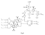
- Figure 3 depicts an operative example of the implementation of the basic processing cell.
- the design has been executed for a standard CMOS technology of 0.13 ⁇ m and 1.5V.
- the dimensions of each of the transistors comprising the proposed processing circuitry are depicted, as are the digital logic gates used, which come from the standard technology library.
- the pre-charge/discharge capability and the supply voltage are also depicted.
- the mapping between the different elements of the circuit enumerated in Figure 2 may be seen, and their correspondence in Figure 3 .
- the voltage-dependent power source is deployed by means of a single nMOS transistor.
- switches (2) and (3) are also deployed by a single transistor, pMOS and nMOS respectively
- switches (9) and (10) each require a respective transmission gate, each of which is comprised of 2 transistors, one nMOS and the other pMOS.
- a precharge interval of at least 50ns is required. The reading of the result of the operation via the V m ij and V M ij voltages could be executed after at least 300ns subsequent to the completion of said pre-charging interval. This is the approximate time required to complete the detection of the edges, accounting for a V px ij signal range of ⁇ [0.75,1.5]V.
Landscapes
- Engineering & Computer Science (AREA)
- Physics & Mathematics (AREA)
- General Physics & Mathematics (AREA)
- Theoretical Computer Science (AREA)
- Multimedia (AREA)
- Software Systems (AREA)
- Nonlinear Science (AREA)
- Analogue/Digital Conversion (AREA)
- Transforming Light Signals Into Electric Signals (AREA)
- Image Analysis (AREA)
Abstract
Description
- The object of the present invention is a hardware device which enables the detection of local maxima and minima in the processing of an image. The hardware which is the object of this invention is included within the framework of the so-called Winner-Take-All (WTA) or Loser-Take-All (LTA) circuits. The scientific-technical area of the invention is that of physical technologies; specifically micro-electronics. Its general scope of application would be that of electronic devices with very low power consumption designed to carry out artificial vision operations; that is, the capture of images, the analysis of the same and the taking of action should this be required by the results of said analysis. Numerous examples of specific applications of these devices might be suggested here: the monitoring of industrial processes, the monitoring of natural spaces, the automatic surveillance of public places, robotics, or to aid unmanned aerial navigation, among others.
- The functions implemented by this invention - the detection of local maxima and minima in an image - may be performed in different ways. One option is by means of general-purpose calculation digital systems. These systems may be programmed to process images, obtaining a result similar to that of the hardware proposed herein. To cite an example, a typical scenario might be the development of software for the analysis of images on a PC. This software would execute a series of instructions by means of the corresponding microprocessor until the desired result is achieved. The main advantage of this approach is the flexibility to undertake any type of task due to the generalistic nature of the underlying hardware. However, this advantage becomes a drawback when the specifications of a particular application require only a limited array of the functions provided by this type of system, but with a much lower power consumption and similar or even higher levels of performance, with regard to the number of operations per second. The non-specific nature of the hardware is precisely what prevents the fulfilment of said requirements on the majority of occasions. It is, however, possible to find a number of alternatives from the purely digital point of view, where the hardware may be progressively adjusted in order to obtain better performance parameters. Thus, we could consider the possibility of using digital signal processors optimised for the execution of certain operations which are useful for the processing of images, such as convolution, for example. Another option might be the implementation of processing primitives in reconfigurable integrated circuits such as FPGAs (Field-Programmable Gate Arrays) or CPLDs (Complex Programmable Logic Devices). As a last resort, digital circuitry specific for a particular application could be designed and integrated in a chip, thus obtaining the highest levels of performance and energetic efficiency.
- The present invention falls beyond the context of exclusively digital implementation described above, and therefore differs in essence from any methodology based on the same. The fundamental difference lies in that, although in our case the basis is also the design of specific hardware for its integration in a chip, this hardware makes use of mixed signal circuitry, handling both analogue and digital signals. This characteristic enables the maximum exploitation of the physics of the transistors when processing the electrical signals representing the pixel values of an image, enabling the obtaining of better performance and power consumption values than an equivalent digital implementation. Many examples may be found reported in the literature concerning mixed signal circuitry for the processing of images [C. N. Stevenson, R. M. Lesperance, F. J. Schauerte and J. R. Troxell, "Image sensor method and apparatus having hardware implemented edge detection processing,"
US Patent 2003/0108221 A1, 12/06/2003 ; J. Dubois, D. Ginhac, M. Paindavoine, and B. Heyrman, "A 10000 FPS CMOS sensor with massively parallel image processing," IEEE J. Solid-State Circuits, vol. 43, no. 3, pp. 706-717, 2008 ; P. Dudek, "SCAMP-3: A vision chip with SIMD current-mode analogue processor array," Focal-plane Sensor-Processor Chips, published by Springer, 2011 ; J. Fernandez Berni, R. Carmona Galin and Luis Carranza Gonzalez, "FLIP-Q: A QCIF resolution focal-plane array for low-power image processing," IEEE J. Solid-State Circuits, vol. 46, no. 3, pp. 669-680, 2011 ]. - The above examples are based on the processing architecture described in [Á. Rodríguez Vázquez, S. Espejo Meana and R. Domínguez Castro, "Programmable mixed-signal integrated circuit architecture for the production of autonomous vision systems in a single chip and/or pre-processing of images in higher-level systems,"
Patent EP 1 580 814 (A1), 28/09/2005 ]. This architecture is characterised by a two-dimensional array of interconnected elemental processors concurrently working together to perform a particular operation on an image. - The present invention is also supported by this processing hardware structure, as are other implementations [B. Amir and H. Saied, "Full CMOS minsum analog iterative decoders,"
Patent US2005240647 (A1 ); L.A. Sánchez-Gaspariano, A. Díaz-Sánchez, G. Saldaña-González, "High-precision current-based CMOS WTA/LTA filters," Int. Conference on Electronics, Communications and Computers, 2007 ; M. Rahman, K. Baishnab, and F. Talukdar, "A high speed and high resolution VLSI winner-take-all circuit for neural networks and fuzzy systems," Int. Symp. on Signals, Circuits and Systems, 2009 ; M. T. Moro-Frias, D. and Sanz-Pascual and C. A. de la Cruz Blas, "A novel current-mode winner-take-all topology," European Conf. on Circuit Theory and Design, 2011, pp. 134-137 ; B. Tomatsopoulos and A. Demosthenous, "Low power, low complexity CMOS multiple-input replicating current comparators and WTA/LTA circuits," European Conf. on Circuit Theory and Design, 2005, pp. 241-244 ; H. Hung-Yi, T. Kea-Tiong, T. Zen-Huan, and C. Hsin, "A low-power, high-resolution WTA utilizing translinear-loop pre-amplifier," Int. Conf. on Neural Networks, 2010 ; R. Dlugosz and T. Talaska, "A low power current-mode binary-tree WTA/LTA circuit for Kohonen neural networks," Int. Conf. on Mixed Design of Integrated Circuits and Systems, 2009, pp. 201-204] with the same functions, but whose mixed signal circuitry differs from that proposed in this specification. It is precisely this original circuitry which enables the obtaining of a much lower power consumption than any other hardware previously reported. - The hardware which is the object of this invention is included within the framework of the so-called Winner-Take-All (WTA) or Loser-Take-All (LTA) circuits. These circuits enable the assessment of the highest value - WTA - and lowest value - LTA - in an array of input signals. Said signals may be represented either by voltages or by intensities. Specifically, when applied to the processing of images, the WTA and LTA hardware blocks enable the detection of the local edges of an image; that is, those pixels whose values are the highest - maximum - or the lowest - minimum - with regard to their eight neighbouring pixels.
- P201030867-137]. In this approach, the operation is supported by an array of similar processing cells, each managed by the corresponding input signal to be processed. These cells are interconnected by means of a common power source in such a way that a concurrent "competition" arises among all the cells in order to obtain the greatest quantity possible of said power. Ultimately, only one of the cells will remain active, either the winner or the loser, according to the configuration selected.
- The other approach is not based on a concurrent interaction of all the signals to be processed, but on a pair processing tree [B. Tomatsopoulos and A. Demosthenous, "Low power, low complexity CMOS multiple-input replicating current comparators and WTA/LTA circuits," European Conf. on Circuit Theory and Design, 2005, pp. 241-244 ; H. Hung-Yi, T. Kea-Tiong, T. Zen-Huan, and C. Hsin, "A low-power, high-resolution WTA utilizing translinear-loop pre-amplifier," Int. Conf. on Neural Networks, 2010 ]. Thus, the array of signals to be processed is divided into pairs and compared at a first processing level. Only the winners - WTA - or the losers - LTA - reach the next processing level, where comparisons by pairs are performed once again. Ultimately, subsequent to performing the comparison at the final level, the global winner or loser will be obtained.
- There also exist a number of hardware structures which may be considered to be hybrid with regard to the above description [R. Dlugosz and T. Talaska, "A low power current-mode binary-tree WTA/LTA circuit for Kohonen neural networks," Int. Conf. on Mixed Design of Integrated Circuits and Systems, 2009, pp. 201-204 ].
- The WTA-LTA circuit for detection of local edges in an image, which is the object of this invention, operates in voltage mode, and its operation is not similar to any of the approaches described above. Specifically, the operation is based on the pre-charging of a condenser and its subsequent discharge by means of a power source dependent on the voltage representing the pixel concerned. Said discharge is compared constantly with that produced in the neighbouring pixels via digital logical gates, a NOR gate for calculation of the minima and a NAND gate for calculation of the maxima. The result of said comparison is stored in a memory feature whose digital output will be read appropriately in accordance with the type of edge to be detected.
- Specifically, the object of the present invention is a device for the hardware detection of local edges in an image, comprised of a plurality of elemental cells (0) for mixed signal processing, locally interconnected in such a way that each cell is only interconnected with its eight neighbouring cells, there being no direct interaction beyond this periphery, and characterised in that each cell comprises at least one first switch (1) configured to enable the pre-charging of a condenser (4) at the supply voltage; and where once said condenser (4) is pre-charged, it discharges via a second switch (2) connected to a power supply (3) which varies in a monotonically increasing manner with the analogue voltage representing the value of the pixel concerned; and where the value of the pixel is compared asynchronously with the neighbouring pixels of the neighbouring cells via two inverters (5,6), a digital NOR gate (7), a digital NAND gate (8), a third and fourth switch (9,10) and a memory feature (11) to store the result.
- The inverters (5,6) bring about a change in the output signal of the second inverter (6) exactly at the instant in time when the discharge of the condenser (4) causes its voltage to cross the input threshold voltage of the first inverter (5), the output of the inverter (6) being connected to the input of the corresponding digital NOR (7) and NAND (8) gates of its neighbouring cells and to the input of a memory feature (11).
- On activation of its output switch (9), a digital NOR gate (7) enables the determination as to whether its associated pixel value constitutes a local minimum; to this end it should be connected to the input of the clock of the memory feature (11).
- Likewise, on activation of its output switch (10), a digital NAND gate (8) enables the determination as to whether its associated pixel value constitutes a local maximum; to this end it should be connected to the input of the clock of the memory feature (11).
- Likewise, an object of the present invention also comprises a method for the hardware detection of local edges in an image, comprised of a plurality of elemental cells (0) for mixed signal processing, locally interconnected with each other in such a way that each cell is only interconnected with its eight neighbouring cells, there being no direct interaction beyond this periphery, put into effect in a device which is the object of the invention and which is characterised in that it comprises a first stage of pre-charging a condenser (4) and its subsequent discharge via a power source (3) dependent on the voltage representing the pixel concerned; and a second stage where said discharge is compared constantly with that produced in the neighbouring pixels via digital logical gates, a NOR gate (7) for calculation of the minima and a NAND gate (8) for calculation of the maxima; and where the result of said comparison is stored in a memory feature (11) whose digital output will be read appropriately in accordance with the type of edge to be detected.
- The device of the invention will be formed by identical elemental cells for the processing of mixed signals which form a plurality by means of their grouping and local interconnection. By "local" it is understood that each cell is interconnected only with its eight neighbouring cells, there being no direct interaction beyond that periphery.
- Throughout the description and the claims, the word "comprise" and its variants shall not exclude other technical characteristics, addenda, components or steps. For those skilled in the art, other objects, advantages and characteristics of the invention will become apparent in part from the description and in part from the practice of the invention. The following examples and drawings are provided for illustrative purposes, and are not intended to be limitative of the present invention. Furthermore, the present invention covers all possible combinations of preferred and particular embodiments indicated herein.
-
-
Figure 1 : the basic structure of the proposed hardware, i.e. a regular two-dimensional spatial distribution of identical locally interconnected processing cells. -
Figure 2 : an elemental processing unit of the regular spatial distribution depicted inFigure 1 . -
Figure 3 : an example of an embodiment of the elemental processing unit depicted inFigure 2 . This example has been designed for a standard CMOS technology of 0.13µm and 1.5V. - In essence, the device of the invention features a plurality of cells, where each cell features at least one switch (1) which enables the pre-charging of the condenser (4) at supply voltage. Next, once pre-charged, it is discharged via the switch (2) connecting it to the power source (3) whose fundamental characteristic lies in that it varies in a monotonically increasing manner with the analogue voltage Vpx
ij representing the value of the pixel concerned. Thus, values greater than Vpsij entail higher voltage and vice versa. This implies that the time interval taken by the voltage Vdij to reach the input threshold voltage of the first inverter (5) will depend on said pixel voltage. This information, that of the crossing between Vdij and the input threshold voltage of the inverter (5), is distributed to the neighbours of the cell under study via the switchover of the Voij voltage from '1' logic to '0' logic. This voltage is the output voltage of the second inverter (6). In turn, the Vomn voltages from the neighbouring cells assume the role of inputs to the current cell. More specifically, they constitute the inputs of two digital gates, one NOR (7) and one NAND (8). The NOR gate (7) enables the detection of the minimum among the neighbouring pixels and the current pixel, while the NAND gate (8) enables detection of the maximum. To this end, either switch (9) or switch (10) respectively should be activated. Finally, the result of the operation performed, this being the detection of either the minimum or the maximum, is stored in a memory feature, specifically a D-type flip-flop (11). Thus, a '1' logic at Vmij indicates that the current pixel is a minimum, while a '1' logic at VMij indicates that the current pixel is a maximum. - Our invention might be defined, in general terms, as low power-consumption hardware based on mixed signal circuitry for the detection of local maxima and minima in an image. It is characterised by a regular two-dimensional spatial distribution of identical locally interconnected processing cells, as depicted in
Figure 1 . Each cell features, at least, the circuitry depicted inFigure 2 , the object of this invention. The operation of detecting the local edges is carried out as follows. During a certain time interval, the digital 'CTRL' signal which operates both switches (1) and (2) should be set at '0' logic. This entails the pre-charging of the condenser (4) at the supply voltage VDD . Once said pre-charging is complete, 'CTRL' should be switched to '1' logic, and from that moment on, the detection of the corresponding edge, maximum or minimum, occurs asynchronously, i.e. without the intervention of any signal from an external clock controlling the operation. At the instant when 'CTRL' switches to '1' logic, this enables the discharge of the condenser (4) via a power source whose fundamental characteristic lies in that it varies in a monotonically increasing manner with the analogue voltage Vpxij representing the value of the pixel concerned. Thus, the voltage provided by said source will be higher for values greater than Vpxij and vice versa. This implies that the time interval required for the voltage Vdij to cross the input threshold voltage of the inverter (5) will ultimately depend on Vpxij . The instant in time tc when this crossing occurs becomes known to the neighbouring cells via the switchover of the Voij voltage from '1' logic to '0' logic. This voltage corresponds to the output of the second inverter (6). In turn, the Vomn voltages from the neighbouring cells constitute inputs to the current cell. More specifically, they constitute inputs of two digital gates, a NOR gate (7) and a NAND gate (8). The NOR gate is associated with the detection of the minimum. Just when 'CRTL' switches from '0' to '1', all its inputs are logic '1's, as all the condensers are pre-charged to VDD. As the discharge process progresses in all the cells, each of these inputs will switch to '0' until finally the last one will do this at the instant in time tm . At that instant in time, if the 'EN_EX' signal which controls the switches (9) and (10) is set at '1', the input of the D-type flip-flop (11) will be captured and stored. If the discharge of the condenser (4) associated with the current cell is the slowest, in comparison with that of its neighbours, the current pixel is a local minimum, in accordance with the aforementioned dependence of its value on the power source. This will be reflected by a logic '1' at Vmij , as at tm the flip-flop input will be a logic '1'. Conversely, if the discharge is not the slowest, the pixel is not a minimum, and the flip-flop input at tm will correspond to a logic '0', a value which will be stored at Vmij . Likewise, the NAND gate enables the detection of a local maximum, on condition that 'EN_EX' is set at '0'. In this case, the switchover of any of its inputs from '1' to '0' entails the storing of the flip-flop input signal at that instant in time; let us call it tM . If said input remains at '1' at tM , this means that the discharge is not the most rapid in comparison with that of its neighbours, and therefore the pixel is not a local maximum. This will imply the storage of a logic '0' at Vmij . Conversely, if the flip-flop input switched over to '0' prior to tM , the current discharge is the most rapid, and therefore the pixel constitutes a local maximum. As a result, a logic '1' will be stored at Vmij . -
Figure 3 depicts an operative example of the implementation of the basic processing cell. The design has been executed for a standard CMOS technology of 0.13µm and 1.5V. In the aforementioned figure the dimensions of each of the transistors comprising the proposed processing circuitry are depicted, as are the digital logic gates used, which come from the standard technology library. The pre-charge/discharge capability and the supply voltage are also depicted. Likewise, the mapping between the different elements of the circuit enumerated inFigure 2 may be seen, and their correspondence inFigure 3 . The voltage-dependent power source is deployed by means of a single nMOS transistor. On the other hand, while switches (2) and (3) are also deployed by a single transistor, pMOS and nMOS respectively, switches (9) and (10) each require a respective transmission gate, each of which is comprised of 2 transistors, one nMOS and the other pMOS. Finally, for the circuit inFigure 3 , a precharge interval of at least 50ns is required. The reading of the result of the operation via the Vmij and VMij voltages could be executed after at least 300ns subsequent to the completion of said pre-charging interval. This is the approximate time required to complete the detection of the edges, accounting for a Vpxij signal range of ∈ [0.75,1.5]V.
Claims (9)
- A device for the hardware detection of local edges in an image, comprised of a plurality of elemental cells (0) for mixed signal processing, locally interconnected in such a way that each cell is only interconnected with its eight neighbouring cells, there being no direct interaction beyond this periphery, and characterised in that each cell comprises at least one first switch (1) configured to enable the pre-charging of a condenser (4) at the supply voltage; and where once said condenser (4) is pre-charged, it discharges via a second switch (2) connected to a power supply (3) which varies in a monotonically increasing manner with the analogue voltage representing the value of the pixel concerned; and where the value of the pixel is compared asynchronously with the neighbouring pixels of the neighbouring cells via two inverters (5,6), a digital NOR gate (7), a digital NAND gate (8), a third and fourth switch (9,10) and a memory feature (11) to store the result.
- A device as claimed in claim 1, where the inverters (5,6) bring about a change in the output signal of the second inverter (6) exactly at the instant in time when the discharge of the condenser (4) causes its voltage to cross the input threshold voltage of the first inverter (5).
- A device as claimed in any of claims 1 to 2, where the output of the inverter (6) is connected to the input of the corresponding digital NOR (7) and NAND (8) gates of its neighbouring cells.
- A device as claimed in any of claims 1 to 3, where the output of the inverter (6) is connected to the input of a memory feature (11).
- A device as claimed in any of claims 1 to 4, where a digital NOR gate (7) enables by means of the activation of its output switch (9) the determination of whether its associated pixel value constitutes a local minimum.
- A device as claimed in any of claims 1 to 5, where the output of the NOR gate (7) should be connected to the input of the clock of the memory feature (11) by means of the activation of the switch (9) to carry out the determination of whether its associated pixel value constitutes a local minimum.
- A device as claimed in any of claims 1 to 6, where a digital NAND gate (8) enables by means of the activation of its output switch (10) the determination of whether its associated pixel value constitutes a local maximum.
- A device as claimed in any of claims 1 to 7, where the output of the NAND gate (8) should be connected to the input of the clock of the memory feature (11) by means of the activation of the switch (10) to carry out the determination of whether its associated pixel value constitutes a local maximum.
- A method for the hardware detection of local edges in an image, comprised of a plurality of elemental cells (0) for mixed signal processing, locally interconnected with each other in such a way that each cell is only interconnected with its eight neighbouring cells, there being no direct interaction beyond this periphery, put into effect in a device as claimed in any of claims 1 to 8 and which is characterised in that it comprises a stage of pre-charging a condenser (4) and its subsequent discharge via a power source (3) dependent on the voltage representing the pixel concerned; and a second stage where said discharge is compared constantly with that produced in the neighbouring pixels via digital logical gates, a NOR gate (7) for calculation of the minima and a NAND gate (8) for calculation of the maxima; and where the result of said comparison is stored in a memory feature (11) whose digital output will be read appropriately in accordance with the type of edge to be detected.
Applications Claiming Priority (2)
| Application Number | Priority Date | Filing Date | Title |
|---|---|---|---|
| ES201201011A ES2459869B2 (en) | 2012-10-08 | 2012-10-08 | Device for hardware detection of local extremes in an image |
| PCT/ES2013/000225 WO2014057146A1 (en) | 2012-10-08 | 2013-10-08 | Device for the hardware detection of local extremes in an image |
Publications (2)
| Publication Number | Publication Date |
|---|---|
| EP2905741A1 true EP2905741A1 (en) | 2015-08-12 |
| EP2905741A4 EP2905741A4 (en) | 2016-09-21 |
Family
ID=50476964
Family Applications (1)
| Application Number | Title | Priority Date | Filing Date |
|---|---|---|---|
| EP13844709.9A Withdrawn EP2905741A4 (en) | 2012-10-08 | 2013-10-08 | DEVICE FOR HARDWARE DETECTION OF LOCAL ENDS IN AN IMAGE |
Country Status (4)
| Country | Link |
|---|---|
| US (1) | US9311559B2 (en) |
| EP (1) | EP2905741A4 (en) |
| ES (1) | ES2459869B2 (en) |
| WO (1) | WO2014057146A1 (en) |
Families Citing this family (1)
| Publication number | Priority date | Publication date | Assignee | Title |
|---|---|---|---|---|
| TWI620687B (en) * | 2017-01-24 | 2018-04-11 | 林清富 | Control system for uav and intermediary device and uav thereof |
Family Cites Families (5)
| Publication number | Priority date | Publication date | Assignee | Title |
|---|---|---|---|---|
| US7151844B2 (en) | 2001-12-06 | 2006-12-19 | General Motors Corporation | Image sensor method and apparatus having hardware implemented edge detection processing |
| ES2209642B1 (en) | 2002-11-04 | 2005-10-01 | Innovaciones Microelectronicas, S.L. | MIXED SIGNAL PROGRAMMED INTEGRATED CIRCUIT ARCHITECTURE FOR THE PERFORMANCE OF AUTONOMOUS VISION SYSTEMS OF A SINGLE CHIP AND / OR PRE-PROCESSING OF IMAGES IN HIGHER LEVEL SYSTEMS. |
| US7126512B2 (en) * | 2004-03-19 | 2006-10-24 | Charles Douglas Murphy | Comparing circuits for time-to-threshold A/D conversion in digital imaging arrays |
| US7769798B2 (en) | 2004-04-27 | 2010-08-03 | Amir Banihashemi | Full CMOS min-sum analog iterative decoders |
| JP2011211474A (en) * | 2010-03-30 | 2011-10-20 | Sony Corp | Image processing apparatus and image signal processing method |
-
2012
- 2012-10-08 ES ES201201011A patent/ES2459869B2/en not_active Expired - Fee Related
-
2013
- 2013-10-08 WO PCT/ES2013/000225 patent/WO2014057146A1/en not_active Ceased
- 2013-10-08 EP EP13844709.9A patent/EP2905741A4/en not_active Withdrawn
- 2013-10-08 US US14/434,212 patent/US9311559B2/en not_active Expired - Fee Related
Also Published As
| Publication number | Publication date |
|---|---|
| ES2459869A1 (en) | 2014-05-12 |
| WO2014057146A1 (en) | 2014-04-17 |
| US20150310298A1 (en) | 2015-10-29 |
| EP2905741A4 (en) | 2016-09-21 |
| ES2459869B2 (en) | 2014-12-04 |
| US9311559B2 (en) | 2016-04-12 |
Similar Documents
| Publication | Publication Date | Title |
|---|---|---|
| JP7012073B2 (en) | Binary neural network on programmable integrated circuit | |
| US20150310311A1 (en) | Dynamically reconstructable multistage parallel single instruction multiple data array processing system | |
| US7098437B2 (en) | Semiconductor integrated circuit device having a plurality of photo detectors and processing elements | |
| EP3352113A1 (en) | Calculation system and calculation method of neural network | |
| US20120136913A1 (en) | System and method for cognitive processing for data fusion | |
| Komuro et al. | A dynamically reconfigurable SIMD processor for a vision chip | |
| US20160274643A1 (en) | Event-based sensor and operating method of processor | |
| US20160247080A1 (en) | Storage device with configurable neural networks | |
| GB2585609A (en) | Hardware to implement a convolutional neural network | |
| US20200210818A1 (en) | Array device including neuromorphic element and neural network system | |
| EP3340067A1 (en) | Median determination | |
| US11309026B2 (en) | Convolution operation method based on NOR flash array | |
| Suárez et al. | Low-power CMOS vision sensor for Gaussian pyramid extraction | |
| US12001945B2 (en) | Event driven mathematical engine and method | |
| Kumar et al. | Low‐latency median filter core for hardware implementation of 5× 5 median filtering | |
| CN112966814A (en) | Information processing method of fused impulse neural network and fused impulse neural network | |
| Reiter et al. | FPGA acceleration of a quantized neural network for remote-sensed cloud detection | |
| WO2022204384A1 (en) | Reconfigurable, hyperdimensional, neural network architecture | |
| US9311559B2 (en) | Device for the hardware detection of local extremes in an image | |
| Cong et al. | CAN: Contextual aggregating network for semantic segmentation | |
| JP6489295B1 (en) | Array apparatus and neural network system including neuromorphic elements | |
| Dudek | A flexible global readout architecture for an analogue SIMD vision chip | |
| Vasanth et al. | FPGA implementation of optimized sorting network algorithm for median filters | |
| Ngo et al. | Real time iris segmentation on FPGA | |
| US9501712B2 (en) | Device for detecting edges and improving the quality of an image |
Legal Events
| Date | Code | Title | Description |
|---|---|---|---|
| PUAI | Public reference made under article 153(3) epc to a published international application that has entered the european phase |
Free format text: ORIGINAL CODE: 0009012 |
|
| 17P | Request for examination filed |
Effective date: 20150508 |
|
| AK | Designated contracting states |
Kind code of ref document: A1 Designated state(s): AL AT BE BG CH CY CZ DE DK EE ES FI FR GB GR HR HU IE IS IT LI LT LU LV MC MK MT NL NO PL PT RO RS SE SI SK SM TR |
|
| AX | Request for extension of the european patent |
Extension state: BA ME |
|
| DAX | Request for extension of the european patent (deleted) | ||
| RA4 | Supplementary search report drawn up and despatched (corrected) |
Effective date: 20160824 |
|
| RIC1 | Information provided on ipc code assigned before grant |
Ipc: G06T 1/20 20060101ALI20160818BHEP Ipc: G06T 1/00 20060101AFI20160818BHEP Ipc: G06K 9/56 20060101ALI20160818BHEP Ipc: G06K 9/00 20060101ALI20160818BHEP Ipc: G06K 9/46 20060101ALI20160818BHEP |
|
| STAA | Information on the status of an ep patent application or granted ep patent |
Free format text: STATUS: REQUEST FOR EXAMINATION WAS MADE |
|
| STAA | Information on the status of an ep patent application or granted ep patent |
Free format text: STATUS: EXAMINATION IS IN PROGRESS |
|
| 17Q | First examination report despatched |
Effective date: 20180625 |
|
| STAA | Information on the status of an ep patent application or granted ep patent |
Free format text: STATUS: THE APPLICATION IS DEEMED TO BE WITHDRAWN |
|
| 18D | Application deemed to be withdrawn |
Effective date: 20180906 |