EP2904634B1 - Combined etch and passivation of silicon solar cells - Google Patents
Combined etch and passivation of silicon solar cells Download PDFInfo
- Publication number
- EP2904634B1 EP2904634B1 EP13789495.2A EP13789495A EP2904634B1 EP 2904634 B1 EP2904634 B1 EP 2904634B1 EP 13789495 A EP13789495 A EP 13789495A EP 2904634 B1 EP2904634 B1 EP 2904634B1
- Authority
- EP
- European Patent Office
- Prior art keywords
- substrate
- silicon
- process according
- steps
- etching
- Prior art date
- Legal status (The legal status is an assumption and is not a legal conclusion. Google has not performed a legal analysis and makes no representation as to the accuracy of the status listed.)
- Active
Links
Images

Classifications
-
- H—ELECTRICITY
- H10—SEMICONDUCTOR DEVICES; ELECTRIC SOLID-STATE DEVICES NOT OTHERWISE PROVIDED FOR
- H10P—GENERIC PROCESSES OR APPARATUS FOR THE MANUFACTURE OR TREATMENT OF DEVICES COVERED BY CLASS H10
- H10P72/00—Handling or holding of wafers, substrates or devices during manufacture or treatment thereof
- H10P72/04—Apparatus for manufacture or treatment
- H10P72/0402—Apparatus for fluid treatment
- H10P72/0418—Apparatus for fluid treatment for etching
- H10P72/0421—Apparatus for fluid treatment for etching for drying etching
-
- H—ELECTRICITY
- H10—SEMICONDUCTOR DEVICES; ELECTRIC SOLID-STATE DEVICES NOT OTHERWISE PROVIDED FOR
- H10F—INORGANIC SEMICONDUCTOR DEVICES SENSITIVE TO INFRARED RADIATION, LIGHT, ELECTROMAGNETIC RADIATION OF SHORTER WAVELENGTH OR CORPUSCULAR RADIATION
- H10F71/00—Manufacture or treatment of devices covered by this subclass
- H10F71/121—The active layers comprising only Group IV materials
-
- H—ELECTRICITY
- H10—SEMICONDUCTOR DEVICES; ELECTRIC SOLID-STATE DEVICES NOT OTHERWISE PROVIDED FOR
- H10F—INORGANIC SEMICONDUCTOR DEVICES SENSITIVE TO INFRARED RADIATION, LIGHT, ELECTROMAGNETIC RADIATION OF SHORTER WAVELENGTH OR CORPUSCULAR RADIATION
- H10F71/00—Manufacture or treatment of devices covered by this subclass
- H10F71/129—Passivating
-
- H—ELECTRICITY
- H10—SEMICONDUCTOR DEVICES; ELECTRIC SOLID-STATE DEVICES NOT OTHERWISE PROVIDED FOR
- H10F—INORGANIC SEMICONDUCTOR DEVICES SENSITIVE TO INFRARED RADIATION, LIGHT, ELECTROMAGNETIC RADIATION OF SHORTER WAVELENGTH OR CORPUSCULAR RADIATION
- H10F77/00—Constructional details of devices covered by this subclass
- H10F77/70—Surface textures, e.g. pyramid structures
- H10F77/703—Surface textures, e.g. pyramid structures of the semiconductor bodies, e.g. textured active layers
-
- H—ELECTRICITY
- H10—SEMICONDUCTOR DEVICES; ELECTRIC SOLID-STATE DEVICES NOT OTHERWISE PROVIDED FOR
- H10P—GENERIC PROCESSES OR APPARATUS FOR THE MANUFACTURE OR TREATMENT OF DEVICES COVERED BY CLASS H10
- H10P72/00—Handling or holding of wafers, substrates or devices during manufacture or treatment thereof
- H10P72/30—Handling or holding of wafers, substrates or devices during manufacture or treatment thereof for conveying, e.g. between different workstations
- H10P72/33—Handling or holding of wafers, substrates or devices during manufacture or treatment thereof for conveying, e.g. between different workstations into and out of processing chamber
- H10P72/3314—Continuous loading and unloading into and out of a processing chamber, e.g. transporting belts within processing chambers
-
- Y—GENERAL TAGGING OF NEW TECHNOLOGICAL DEVELOPMENTS; GENERAL TAGGING OF CROSS-SECTIONAL TECHNOLOGIES SPANNING OVER SEVERAL SECTIONS OF THE IPC; TECHNICAL SUBJECTS COVERED BY FORMER USPC CROSS-REFERENCE ART COLLECTIONS [XRACs] AND DIGESTS
- Y02—TECHNOLOGIES OR APPLICATIONS FOR MITIGATION OR ADAPTATION AGAINST CLIMATE CHANGE
- Y02E—REDUCTION OF GREENHOUSE GAS [GHG] EMISSIONS, RELATED TO ENERGY GENERATION, TRANSMISSION OR DISTRIBUTION
- Y02E10/00—Energy generation through renewable energy sources
- Y02E10/50—Photovoltaic [PV] energy
- Y02E10/547—Monocrystalline silicon PV cells
-
- Y—GENERAL TAGGING OF NEW TECHNOLOGICAL DEVELOPMENTS; GENERAL TAGGING OF CROSS-SECTIONAL TECHNOLOGIES SPANNING OVER SEVERAL SECTIONS OF THE IPC; TECHNICAL SUBJECTS COVERED BY FORMER USPC CROSS-REFERENCE ART COLLECTIONS [XRACs] AND DIGESTS
- Y02—TECHNOLOGIES OR APPLICATIONS FOR MITIGATION OR ADAPTATION AGAINST CLIMATE CHANGE
- Y02P—CLIMATE CHANGE MITIGATION TECHNOLOGIES IN THE PRODUCTION OR PROCESSING OF GOODS
- Y02P70/00—Climate change mitigation technologies in the production process for final industrial or consumer products
- Y02P70/50—Manufacturing or production processes characterised by the final manufactured product
Definitions
- the invention relates to a process for dry chemical texturing of a substrate. More particularly, the invention relates to a process for a combined dry chemical etching and passivation of a substrate (for example, silicon-based photovoltaic (PV) devices).
- a substrate for example, silicon-based photovoltaic (PV) devices.
- etching steps are required in the manufacturing of solar cells.
- the front side of the cell needs to be etched in order to produce a surface texture that will lower the reflectivity of the wafer.
- Si etching processes use halogen, and more specifically fluorinated chemistry as described in CN 101 880 914 A , WO 2010/105703 A1 and WO 2011/141516 A2 .
- Etching alters the surface state of the substrate, and can generate defects that act as recombination centres, degrading the electrical properties of the wafer.
- the etched surface needs to be passivated in a subsequent process step, usually in a different process tool.
- Common passivation processes consist of plasma-enhanced chemical vapour deposition (PECVD) of silicon-nitride layers, or stacks of silicon-oxide and silicon-nitride layers.
- PECVD plasma-enhanced chemical vapour deposition
- the conformality of such passivation method varies. It is usually suitable for a texture feature size of several micrometres. For sub-micrometer size features, these passivation methods are not efficient, resulting in very low carrier lifetime. Yet sub-micron texture have proved to be very efficient as a light trapping feature, resulting in very low surface reflectivity values that have the potential to increase the overall efficiency of the solar cell.
- the problem to be solved by the present invention is to provide a process for etching features of any size without affecting the electrical properties of a substrate suitable for silicon solar cells.
- the process of the present invention can generate a strongly passivated and stable surface texture through a single dry process and tool.
- a process for etching a texture on a surface of a silicon substrate and passivating said substrate surface, wherein the silicon substrate is a silicon wafer or a silicon layer deposited on a substrate comprising the steps of:
- the oxidation needs to be carried out on a fully fluorinated surface, i.e. before the fluorinated surface is to be exposed to air or any other reactive atmosphere that could trigger a chemical reaction at the surface.
- a reactive atmosphere could be, for example, any atmosphere comprising elements which react strongly with fluorine, expect Nitrogen, Helium, Argon, Neon and Krypton.
- the substrate is only exposed to nitrogen or any other neutral gas between the etching step and the oxidation step.
- Atmospheric pressure is more convenient to use, in particular for applications requiring high throughput, like solar cell manufacturing.
- the fluoride-containing gases may be selected from the group comprising tetrafluoromethane, trifluoromethane, carbonyl fluoride, sulphur hexafluoride, nitrogen trifluoride, xenon difluoride, and elemental fluorine.
- the etchant gas is molecular Fluorine.
- the Fluorine concentration can be any concentration in a range of between about 5 to 100%, with or without dilution with N 2 or any other gas that does not react with molecular F 2 , such as for example helium, argon, neon, and krypton.
- Fluorine is known to be very good at passivating silicon surfaces, since the energy of the fluorine-Si bond is significant.
- the process of the present invention is designed to take full advantage of this high passivation properties and the fact that fluorine mixtures are commonly used and readily available as etching gas in both semiconductor and photovoltaic industries.
- the fluorinated gaseous etching process results in a surface fully saturated with fluorine.
- Previous experiments and literature show that fluorinated surfaces are very unstable, and quickly react when in contact with ambient air, mainly reacting with the water vapour.
- the advantage of this invention is that the fluorinated etched surface and its passivation properties can be preserved. This is achieved by capping the surface post-etch with an oxide layer, through a thermal oxidation cycle.
- Each etch gas may have its own method of etching radical formation.
- the substrate for etching, on which the silicon layer is deposited may be selected from glass, AlTiC (Aluminum Titanium Carbon), ITO (Indium tin oxide) and FR4 laminates (woven fibreglass cloth with an epoxy resin binder that is flame resistant).
- AlTiC AlTiC
- ITO Indium tin oxide
- FR4 laminates woven fibreglass cloth with an epoxy resin binder that is flame resistant.
- silicon layer should be understood to encompass all thing films/thin deposited silicon layers and expitaxial silicon layers.
- the process is performed in an atmospheric reaction process and the surface of the etched silicon substrate is performed in the same process chamber or in an additional process chamber without having the substrate come in contact with ambient air by passing the substrate through purge curtains.
- Another significant advantage of this method is that the oxidation rate will be enhanced due to the presence of the etchant gas at the surface of the silicon substrate, considerably reducing the overall thermal budget of the process.
- the etchant gas is molecular fluorine and the preferred oxidising species is ozone (O 3 ).
- the substrate can then be exposed to ambient air and will retain its electrical properties.
- the resulting layer can be a silicon-oxide-fluoride layer, or similar to Fluorinated Silicon Glass (FSG).
- FSG Fluorinated Silicon Glass
- the oxidation step of the process can be combined with a doping step, whereby the doping step involves injection of precursors.
- the precursors are elected from the group comprising tetraethyl orthosilicate (TEOS, Si(OC 2 H 5 ) 4 ), silane and oxygen, dichlorosilane (SiCl 2 H 2 ) and nitrous oxide (N 2 O), trimethylborate (TMB) or triethylborate (TEB), or trimethylphosphate (TMPO) or trimethylphosphite (TMPI), or any combination thereof.
- the silicon oxide is deposited using a mixture of tetraethoxysilane and ozone gases and at least one selected from trimethylborate (TMB), triethylborate (TEB), trimethylphosphate (TMPO), trimethylphosphite (TMPI), diborane, phosphine, and arsine on top of the etched surface.
- TMB trimethylborate
- TEB triethylborate
- TMPO trimethylphosphate
- TMPI trimethylphosphite
- diborane phosphine
- arsine arsine
- all process steps are carried out at a temperature below about 600 deg. C, preferably below about 500 deg. C, more preferably below about 400 deg. C.
- all process steps are carried out either in the same atmospheric reaction apparatus or in a subsequent atmospheric reaction chamber separated by nitrogen gas or other inert gas purge curtains in a continuous system.
- continuous system should be understood to mean that the substrate is constantly moving during each process step, i.e. the substrate velocity is one of the process parameters.
- Subsequent steps required to complete the fabrication of a solar cell would then include annealing, deposition of an anti-reflective layer at the front surface, and contacting of the front and back side of the cell.
- a standard thermal annealing step is required in order to form the emitter, during which the previously deposited dopant atoms are diffused inside the silicon.
- This anneal step commonly used by the solar industry, could either be carried out at atmospheric pressure and in the same tool, or at another location and tool, because the surface of the substrate can safely be exposed to air after the oxidation step.
- the deposition of an anti-reflective layers in order to reduce the reflectivity of the cell, or increase further the passivation consists typically of deposition of a defined thickness of silicon nitride using vacuum based plasma enhance chemical vapour deposition tool (PE-CVD).
- PE-CVD vacuum based plasma enhance chemical vapour deposition tool
- the advantages of the process of the present invention are that the passivation quality of the fluorinated surface of the substrate is preserved and the final passivation of the resulting substrate (wafer) is improved compared to a standard (solar cell) process. Further, the oxidation rate is enhanced by the fluorinated surface and the overall thermal budget of the process is significantly reduced accordingly. Also, the overall efficiency of the finished cell is improved as a result of the improved passivation. Within the context of solar cell manufacturing, using this new process would also lead to significant simplification and reduction of the number of process steps required. Indeed, the atmospheric pressure hardware (as described in WO 2011/141516 ) can deliver a single sided process for both texturing and doping/oxidation.
- the texture and the emitter are formed only at the front side of the cell. Therefore, there is no need to carry out an edge isolation step that is usually required in a standard cell process in order to remove the junction at the back side of the cell.
- the texture created and passivated can be a very efficient light-trapping nano-texture (commonly referred to as "black silicon”), that would not necessarily require the addition of an anti reflective layer (typically SiNx).
- a process for etching a texture on a surface of a silicon substrate and passivating said substrate surface, wherein the silicon substrate is a silicon wafer or a silicon layer deposited on a substrate comprising the steps of:
- the etchant gas is selected from elemental fluorine, elemental chlorine, fluoride-containing compounds or chlorine-containing compounds.
- the fluoride-containing compounds may be selected from the group comprising tetrafluoromethane, trifluoromethane, carbonyl fluoride, sulphur hexafluoride, nitrogen trifluoride, xenon difluoride, and elemental fluorine.
- the chlorine-based compounds may be selected from the group comprising tetrachloromethane, a mixture of trichlorosilane and hydrogen, and hydrogen chloride.
- passivation or “passivate” should be understood to mean a process by which the substrate becomes less affected by environmental factors such as air or water, and the electrical properties of the substrate are preserved or improved. More specifically for solar cell application, a passivating process reduces surface recombination, a significant loss mechanism for this type of device.
- the present invention uses a dry-etch chemistry where the etching is not limited by the crystalline structure of the surface to be etched.
- the etchants are controllably delivered in gaseous form and are applied to the surface to be etched at atmospheric pressure. There is no requirement for the etching zone to be contained in a vacuum chamber, although it is possible to do so.
- FIG. 1 there is illustrated an atmospheric reactor 101 adapted to perform the process of the invention.
- the silicon substrate 103 is placed on a moveable carrier 105, for example, a substrate conveyor, adapted to move continuously to deliver the substrate 103 to an etching zone 107. Only the front side of the substrate is exposed to the process.
- the reaction area 109 is sealed off by purge curtains 111,112 at the entrance and the exit, respectively.
- the etching zone 107 is positioned inside the perimeter boundaries defined by the purge curtains 111,112.
- the conveyor 105 moves the substrate 103 through the etching zone 107 in a controlled manner such that under an etchant-delivering system 115 inside the reactor 107 at least one etchant in gas form is applied under atmospheric pressure to the substrate 103 in the reactor 107.
- the etchant gas is molecular fluorine.
- the etched substrate 103 that has now a front surface fully saturated with fluorine, is moved through the etching area 107 to the oxidation zone 120, passing under a nitrogen purge curtain 113.
- the purge curtain 113 separates the two reacting zones 107 and 120, and prevents the mixing of gases from each section.
- the oxidation of the surface takes place when the now etched substrate 103 enters the oxidation zone 120.
- the chemical precursor gases are introduced via a gas distribution system 117.
- the zone 120 is designed in order to grow/deposit the required thickness of a passivating layer while the substrate 103 is continuously moving through the reacting zone 109.
- the substrate 103 exits the reactor/reaction area 109 where it can be moved on the next processing station.
- the second section of the reactor zone 120 provides the deposition of a doped silicon-oxide layer, by injection of a combination of TEOS, ozone and phosphorus or boron via the combined pre-doping and oxidising application system 119.
- FIG. 3 there is illustrated the same apparatus and process described in Figure 2 but with a buffering station 125 between the two sections 107 and 120 of the reactor 101.
- the substrates 103 arriving from the etching section 107 can be buffered and dispatch to the next section 120 at the appropriate speed required by the next process.
- This buffering section 125 will dissociate the velocity process parameter of the two sequential processes, providing a more flexible overall process control.
- This embodiment requires at least two independent conveyors 105a, 105b, one for each reacting zone and is the preferred configuration in a high throughput industrial environment.
- the process is semi-continuous; a substrate 103 or a batch of substrates are introduced inside a reactive zone 130.
- the conveyor 105 stops, and the first etching step is carried out by injecting the relevant etching gas via the system 115. Once the etching has been done, the precursors required for the oxidation of the surface are then injected via the system 119. Once the oxidation, or deposition of the doped oxide layer is sufficient, the substrate 103 (or batch of substrates) are moved outside the reactive zone 130 where they can be moved on to the next processing station.
- This scenario is more relevant to a tool that does not require delivering a very high throughput, like for example in a laboratory/ R&D setup.
- FIG. 5 there is illustrated the implication of this invention on the overall process flow of solar cell manufacturing.
- the process flow and associated steps for a standard industrial cell process are described.
- the solar cell manufacturing process including the steps of the present invention.
- a standard process requires a succession of wet and dry in-vacuum process steps. Also, most of the steps are carried out on both sides of the wafer. In the process of the present invention, the number of steps and therefore processing tools, are reduced. Because this invention provides a means of doping the substrate before thermal diffusion, and that this doping process can be applied on only one side of the substrate using the hardware described in the previous paragraph, the edge isolation step is no longer required. The resulting manufacturing process requires only between 4 and 5 steps.
Landscapes
- Photovoltaic Devices (AREA)
Description
- The invention relates to a process for dry chemical texturing of a substrate. More particularly, the invention relates to a process for a combined dry chemical etching and passivation of a substrate (for example, silicon-based photovoltaic (PV) devices).
- Several etching steps are required in the manufacturing of solar cells. In particular, the front side of the cell needs to be etched in order to produce a surface texture that will lower the reflectivity of the wafer.
- Most silicon (Si) etching processes use halogen, and more specifically fluorinated chemistry as described in
CN 101 880 914 AWO 2010/105703 A1 andWO 2011/141516 A2 . Etching alters the surface state of the substrate, and can generate defects that act as recombination centres, degrading the electrical properties of the wafer. - In order to reduce these effects, the etched surface needs to be passivated in a subsequent process step, usually in a different process tool. Common passivation processes consist of plasma-enhanced chemical vapour deposition (PECVD) of silicon-nitride layers, or stacks of silicon-oxide and silicon-nitride layers. The conformality of such passivation method varies. It is usually suitable for a texture feature size of several micrometres. For sub-micrometer size features, these passivation methods are not efficient, resulting in very low carrier lifetime. Yet sub-micron texture have proved to be very efficient as a light trapping feature, resulting in very low surface reflectivity values that have the potential to increase the overall efficiency of the solar cell.
- It is an object of the present invention to overcome at least one of the above-mentioned problems.
- The problem to be solved by the present invention is to provide a process for etching features of any size without affecting the electrical properties of a substrate suitable for silicon solar cells. The process of the present invention can generate a strongly passivated and stable surface texture through a single dry process and tool.
- According to the present invention there is provided, as set out in the appended claims, a process for etching a texture on a surface of a silicon substrate and passivating said substrate surface, wherein the silicon substrate is a silicon wafer or a silicon layer deposited on a substrate, the process comprising the steps of:
- inserting a silicon substrate in a reactor chamber; heating the reaction chamber and substrate;
- etching the surface of the substrate with a fluoride-containing etchant gas inside the chamber, while the substrate is being conveyed at a constant velocity; and
- oxidising the textured, fluorinated surface of the substrate without exposing the substrate to air
- wherein the steps are performed at atmospheric pressure and wherein the etchant gas is molecular florine.
- The oxidation needs to be carried out on a fully fluorinated surface, i.e. before the fluorinated surface is to be exposed to air or any other reactive atmosphere that could trigger a chemical reaction at the surface. A reactive atmosphere could be, for example, any atmosphere comprising elements which react strongly with fluorine, expect Nitrogen, Helium, Argon, Neon and Krypton. The substrate is only exposed to nitrogen or any other neutral gas between the etching step and the oxidation step.
- The process is carried out at atmospheric pressure. Atmospheric pressure is more convenient to use, in particular for applications requiring high throughput, like solar cell manufacturing.
- In one example not forming part of the present invention the fluoride-containing gases may be selected from the group comprising tetrafluoromethane, trifluoromethane, carbonyl fluoride, sulphur hexafluoride, nitrogen trifluoride, xenon difluoride, and elemental fluorine.
- The etchant gas is molecular Fluorine. The Fluorine concentration can be any concentration in a range of between about 5 to 100%, with or without dilution with N2 or any other gas that does not react with molecular F2, such as for example helium, argon, neon, and krypton.
- Fluorine is known to be very good at passivating silicon surfaces, since the energy of the fluorine-Si bond is significant. The process of the present invention is designed to take full advantage of this high passivation properties and the fact that fluorine mixtures are commonly used and readily available as etching gas in both semiconductor and photovoltaic industries. The fluorinated gaseous etching process results in a surface fully saturated with fluorine. Previous experiments and literature show that fluorinated surfaces are very unstable, and quickly react when in contact with ambient air, mainly reacting with the water vapour. The advantage of this invention is that the fluorinated etched surface and its passivation properties can be preserved. This is achieved by capping the surface post-etch with an oxide layer, through a thermal oxidation cycle.
- Each etch gas may have its own method of etching radical formation.
- In one embodiment the substrate for etching, on which the silicon layer is deposited, may be selected from glass, AlTiC (Aluminum Titanium Carbon), ITO (Indium tin oxide) and FR4 laminates (woven fibreglass cloth with an epoxy resin binder that is flame resistant).
- In the specification, the term "silicon layer" should be understood to encompass all thing films/thin deposited silicon layers and expitaxial silicon layers.
- The process is performed in an atmospheric reaction process and the surface of the etched silicon substrate is performed in the same process chamber or in an additional process chamber without having the substrate come in contact with ambient air by passing the substrate through purge curtains.
- Another significant advantage of this method is that the oxidation rate will be enhanced due to the presence of the etchant gas at the surface of the silicon substrate, considerably reducing the overall thermal budget of the process.
- The etchant gas is molecular fluorine and the preferred oxidising species is ozone (O3).
- After this process, the substrate can then be exposed to ambient air and will retain its electrical properties. The resulting layer can be a silicon-oxide-fluoride layer, or similar to Fluorinated Silicon Glass (FSG). The substrate can be subsequently transported safely to another processing tool in order to carry out the remaining manufacturing steps, or stored for later processing.
- In one embodiment, the oxidation step of the process can be combined with a doping step, whereby the doping step involves injection of precursors. The precursors are elected from the group comprising tetraethyl orthosilicate (TEOS, Si(OC2H5)4), silane and oxygen, dichlorosilane (SiCl2H2) and nitrous oxide (N2O), trimethylborate (TMB) or triethylborate (TEB), or trimethylphosphate (TMPO) or trimethylphosphite (TMPI), or any combination thereof.
- Preferably, the silicon oxide is deposited using a mixture of tetraethoxysilane and ozone gases and at least one selected from trimethylborate (TMB), triethylborate (TEB), trimethylphosphate (TMPO), trimethylphosphite (TMPI), diborane, phosphine, and arsine on top of the etched surface.
- In one embodiment, all process steps are carried out at a temperature below about 600 deg. C, preferably below about 500 deg. C, more preferably below about 400 deg. C.
- Preferably, all process steps are carried out either in the same atmospheric reaction apparatus or in a subsequent atmospheric reaction chamber separated by nitrogen gas or other inert gas purge curtains in a continuous system. In the specification, the term "continuous system" should be understood to mean that the substrate is constantly moving during each process step, i.e. the substrate velocity is one of the process parameters.
- Subsequent steps required to complete the fabrication of a solar cell would then include annealing, deposition of an anti-reflective layer at the front surface, and contacting of the front and back side of the cell. A standard thermal annealing step is required in order to form the emitter, during which the previously deposited dopant atoms are diffused inside the silicon. This anneal step, commonly used by the solar industry, could either be carried out at atmospheric pressure and in the same tool, or at another location and tool, because the surface of the substrate can safely be exposed to air after the oxidation step.
- The deposition of an anti-reflective layers in order to reduce the reflectivity of the cell, or increase further the passivation, consists typically of deposition of a defined thickness of silicon nitride using vacuum based plasma enhance chemical vapour deposition tool (PE-CVD).
- The advantages of the process of the present invention are that the passivation quality of the fluorinated surface of the substrate is preserved and the final passivation of the resulting substrate (wafer) is improved compared to a standard (solar cell) process. Further, the oxidation rate is enhanced by the fluorinated surface and the overall thermal budget of the process is significantly reduced accordingly. Also, the overall efficiency of the finished cell is improved as a result of the improved passivation. Within the context of solar cell manufacturing, using this new process would also lead to significant simplification and reduction of the number of process steps required. Indeed, the atmospheric pressure hardware (as described in
WO 2011/141516 ) can deliver a single sided process for both texturing and doping/oxidation. This means that the texture and the emitter are formed only at the front side of the cell. Therefore, there is no need to carry out an edge isolation step that is usually required in a standard cell process in order to remove the junction at the back side of the cell. Also, as mentioned previously, the texture created and passivated can be a very efficient light-trapping nano-texture (commonly referred to as "black silicon"), that would not necessarily require the addition of an anti reflective layer (typically SiNx). - In one embodiment of the invention, there is provided a process for etching a texture on a surface of a silicon substrate and passivating said substrate surface, wherein the silicon substrate is a silicon wafer or a silicon layer deposited on a substrate, the process comprising the steps of:
- (a) inserting a silicon substrate into a reaction chamber;
- (b) heating the reaction chamber and silicon substrate;
- (c) etching the surface of the substrate with an etchant gas inside the chamber, while the substrate is being conveyed at a constant velocity; and
- (d) oxidising the textured, fluorinated surface of the substrate without exposing the substrate to air; and
- In one example, not forming part of the invention, the etchant gas is selected from elemental fluorine, elemental chlorine, fluoride-containing compounds or chlorine-containing compounds. The fluoride-containing compounds may be selected from the group comprising tetrafluoromethane, trifluoromethane, carbonyl fluoride, sulphur hexafluoride, nitrogen trifluoride, xenon difluoride, and elemental fluorine. The chlorine-based compounds may be selected from the group comprising tetrachloromethane, a mixture of trichlorosilane and hydrogen, and hydrogen chloride.
- In the specification, the term "passivation" or "passivate" should be understood to mean a process by which the substrate becomes less affected by environmental factors such as air or water, and the electrical properties of the substrate are preserved or improved. More specifically for solar cell application, a passivating process reduces surface recombination, a significant loss mechanism for this type of device.
- The invention will be more clearly understood from the following description of an embodiment thereof, given by way of example only, with reference to the accompanying drawings, in which:-
-
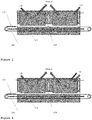
Figure 1 is a diagram illustrating the dry process of the present invention in the case of 2 separate chambers where the etching is carried out within the first section of the reactor and the oxidation is carried out within the following section of the reactor; -
Figure 2 is a diagram illustrating the dry process of the present invention in the case of 2 separate chambers, where the etching is carried out within the first section of the reactor and the deposition of a doped SiOx layer is carried out within the following section of the reactor; -
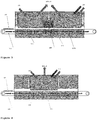
Figure 3 is a diagram illustrating the dry process of the present invention in the case of 2 separate chambers with a buffering station in between the two chambers. -
Figure 4 is a diagram illustrating the dry etching process of the present invention in the case where all the steps are carried out sequentially within a single reactor -
Figure 5 is a flow diagram illustrating the various manufacturing steps for a standard cell process and for a cell process incorporating the present invention (alternative cell process flow), and the resulting simplification. - The present invention uses a dry-etch chemistry where the etching is not limited by the crystalline structure of the surface to be etched. The etchants are controllably delivered in gaseous form and are applied to the surface to be etched at atmospheric pressure. There is no requirement for the etching zone to be contained in a vacuum chamber, although it is possible to do so.
- Referring now to
Figure 1 , there is illustrated anatmospheric reactor 101 adapted to perform the process of the invention. Thesilicon substrate 103 is placed on amoveable carrier 105, for example, a substrate conveyor, adapted to move continuously to deliver thesubstrate 103 to anetching zone 107. Only the front side of the substrate is exposed to the process. Thereaction area 109 is sealed off by purge curtains 111,112 at the entrance and the exit, respectively. - The
etching zone 107 is positioned inside the perimeter boundaries defined by the purge curtains 111,112. Theconveyor 105 moves thesubstrate 103 through theetching zone 107 in a controlled manner such that under an etchant-deliveringsystem 115 inside thereactor 107 at least one etchant in gas form is applied under atmospheric pressure to thesubstrate 103 in thereactor 107. The etchant gas is molecular fluorine. - The etched
substrate 103, that has now a front surface fully saturated with fluorine, is moved through theetching area 107 to theoxidation zone 120, passing under anitrogen purge curtain 113. Thepurge curtain 113 separates the two reactingzones substrate 103 enters theoxidation zone 120. The chemical precursor gases are introduced via agas distribution system 117. Thezone 120 is designed in order to grow/deposit the required thickness of a passivating layer while thesubstrate 103 is continuously moving through the reactingzone 109. Finally, thesubstrate 103 exits the reactor/reaction area 109 where it can be moved on the next processing station. - Referring now to
Figure 2 , there is illustrated the same atmospheric reactor, but this time the second section of thereactor zone 120 provides the deposition of a doped silicon-oxide layer, by injection of a combination of TEOS, ozone and phosphorus or boron via the combined pre-doping and oxidisingapplication system 119. - Referring now to
Figure 3 , there is illustrated the same apparatus and process described inFigure 2 but with abuffering station 125 between the twosections reactor 101. Thesubstrates 103 arriving from theetching section 107 can be buffered and dispatch to thenext section 120 at the appropriate speed required by the next process. Thisbuffering section 125 will dissociate the velocity process parameter of the two sequential processes, providing a more flexible overall process control. This embodiment requires at least twoindependent conveyors - Referring now to
Figure 4 , there is illustrated another embodiment where the etching and oxidation steps are carried out in the same reaction chamber. In this particular case, the process is semi-continuous; asubstrate 103 or a batch of substrates are introduced inside areactive zone 130. Theconveyor 105 stops, and the first etching step is carried out by injecting the relevant etching gas via thesystem 115. Once the etching has been done, the precursors required for the oxidation of the surface are then injected via thesystem 119. Once the oxidation, or deposition of the doped oxide layer is sufficient, the substrate 103 (or batch of substrates) are moved outside thereactive zone 130 where they can be moved on to the next processing station. This scenario is more relevant to a tool that does not require delivering a very high throughput, like for example in a laboratory/ R&D setup. - Referring now to
Figure 5 , there is illustrated the implication of this invention on the overall process flow of solar cell manufacturing. On the left hand side, the process flow and associated steps for a standard industrial cell process are described. On the right side, the solar cell manufacturing process including the steps of the present invention. A standard process requires a succession of wet and dry in-vacuum process steps. Also, most of the steps are carried out on both sides of the wafer. In the process of the present invention, the number of steps and therefore processing tools, are reduced. Because this invention provides a means of doping the substrate before thermal diffusion, and that this doping process can be applied on only one side of the substrate using the hardware described in the previous paragraph, the edge isolation step is no longer required. The resulting manufacturing process requires only between 4 and 5 steps. - In the specification the terms "comprise, comprises, comprised and comprising" or any variation thereof and the terms "include, includes, included and including" or any variation thereof are considered to be totally interchangeable and they should all be afforded the widest possible interpretation and vice versa.
Claims (8)
- A process for etching a texture on a surface of a silicon substrate and passivating said substrate surface, wherein the silicon substrate is a silicon wafer or a silicon layer deposited on a substrate, the process comprising the steps of:(a) inserting a silicon substrate (103) into a reaction chamber (107);(b) heating the reaction chamber and substrate;(c) etching the surface of the substrate with a fluoride-containing etchant gas inside the chamber while the substrate is being conveyed at a constant velocity; and(d) oxidising (120) the textured, fluorinated surface of the substrate without exposing the substrate to air; andwherein the steps are performed at atmospheric pressure and wherein the etchant gas is molecular fluorine.
- A process according to Claim 1, wherein the molecular fluorine can be any concentration in a range of between about 5 to 100%, with or without dilution with N2 or any other gas that does not react with molecular fluorine such as helium, argon, neon, and krypton.
- A process according to any one of Claims 1 to 2, wherein the oxidising species is ozone.
- A process according to any one of the preceding claims, wherein the process further comprises a doping step combined with the oxidising step.
- A process according to Claim 4, wherein the combined oxidation and doping step comprises injection of a precursor into the reaction chamber selected from the group comprising tetraethyl orthosilicate (TEOS, Si(OC2H5)4), silane and oxygen, dichlorosilane (SiCl2H2) and nitrous oxide (N2O), trimethylborate (TMB) or triethylborate (TEB), or trimethylphosphate (TMPO) or trimethylphosphite (TMPI), or any combination thereof; or it comprises optionally depositing a silicon oxide by using a mixture of tetraethoxysilane and ozone gases and at least one selected from trimethylborate (TMB), triethylborate (TEB), trimethylphosphate (TMPO), trimethylphosphite (TMPI), diborane, phosphine, and arsine.
- A process according to any one of the preceding claims, wherein all process steps are carried out in the same atmospheric reaction apparatus; or wherein all process steps are carried out in a subsequent atmospheric reaction chamber separated by nitrogen gas or other inert gas purge curtains in a continuous system.
- A process according to any one of the preceding claims, wherein the process steps are applied on only one side of the substrate.
- A process according to any one of the preceding claims, wherein all process steps are carried out at a temperature below about 600 deg. C.
Applications Claiming Priority (2)
| Application Number | Priority Date | Filing Date | Title |
|---|---|---|---|
| IES20120434 | 2012-10-01 | ||
| PCT/EP2013/070443 WO2014053484A1 (en) | 2012-10-01 | 2013-10-01 | Combined etch and passivation of silicon solar cells |
Publications (2)
| Publication Number | Publication Date |
|---|---|
| EP2904634A1 EP2904634A1 (en) | 2015-08-12 |
| EP2904634B1 true EP2904634B1 (en) | 2020-04-08 |
Family
ID=50434378
Family Applications (1)
| Application Number | Title | Priority Date | Filing Date |
|---|---|---|---|
| EP13789495.2A Active EP2904634B1 (en) | 2012-10-01 | 2013-10-01 | Combined etch and passivation of silicon solar cells |
Country Status (2)
| Country | Link |
|---|---|
| EP (1) | EP2904634B1 (en) |
| WO (1) | WO2014053484A1 (en) |
Families Citing this family (3)
| Publication number | Priority date | Publication date | Assignee | Title |
|---|---|---|---|---|
| CN107968130B (en) * | 2017-11-27 | 2019-05-10 | 乐山新天源太阳能科技有限公司 | Wafer cleaning and texturing process |
| CN107968062B (en) * | 2017-11-27 | 2019-09-13 | 乐山新天源太阳能科技有限公司 | Silicon chip cleaning and texturing device |
| DE102019102492A1 (en) * | 2019-01-31 | 2020-08-06 | Fraunhofer-Gesellschaft zur Förderung der angewandten Forschung e.V. | Device and method for processing wafers |
Family Cites Families (4)
| Publication number | Priority date | Publication date | Assignee | Title |
|---|---|---|---|---|
| US20020111011A1 (en) * | 2001-02-15 | 2002-08-15 | King-Lung Wu | Method for forming a contact plug without a dimple surface |
| WO2010105703A1 (en) * | 2009-03-17 | 2010-09-23 | Interuniversitair Microelektronica Centrum Vzw (Imec) | Method for plasma texturing |
| PL2569802T3 (en) | 2010-05-11 | 2018-01-31 | Ultra High Vacuum Solutions Ltd T/A Nines Eng | A method of controlling the modification of the surface texture of a silicon wafer for devices in the form of photovoltaic cells |
| CN101880914B (en) * | 2010-05-25 | 2012-09-12 | 中国科学院微电子研究所 | Method for preparing black silicon by plasma immersion ion implantation |
-
2013
- 2013-10-01 WO PCT/EP2013/070443 patent/WO2014053484A1/en not_active Ceased
- 2013-10-01 EP EP13789495.2A patent/EP2904634B1/en active Active
Non-Patent Citations (1)
| Title |
|---|
| None * |
Also Published As
| Publication number | Publication date |
|---|---|
| HK1213693A1 (en) | 2016-07-08 |
| WO2014053484A1 (en) | 2014-04-10 |
| EP2904634A1 (en) | 2015-08-12 |
Similar Documents
| Publication | Publication Date | Title |
|---|---|---|
| EP4203081A1 (en) | Topcon battery and preparation method therefor, and electrical appliance | |
| US7846762B2 (en) | Integrated emitter formation and passivation | |
| KR102489044B1 (en) | Deposition Methods for Uniform and Conformal Hybrid Titanium Oxide Films | |
| JP2013524510A5 (en) | ||
| US9548224B2 (en) | Method and apparatus to control surface texture modification of silicon wafers for photovoltaic cell devices | |
| JP2011503848A (en) | Plasma treatment during the deposition process | |
| CA2704389A1 (en) | Transparent conductive oxide coating for thin film photovoltaic applications and methods of making the same | |
| CN113675295A (en) | Method for preparing silicon wafer composite membrane by PECVD and preparation method of TOPCon battery | |
| US5629246A (en) | Method for forming fluorine-doped glass having low concentrations of free fluorine | |
| US20250132201A1 (en) | Nucleation-free deposition | |
| EP4411841A1 (en) | Solar cell and preparation method therefor | |
| US20100210060A1 (en) | Double anneal process for an improved rapid thermal oxide passivated solar cell | |
| US7981778B2 (en) | Directional solid phase crystallization of thin amorphous silicon for solar cell applications | |
| CN113481487A (en) | Solar cell and back surface PECVD method and application thereof | |
| WO2014053484A1 (en) | Combined etch and passivation of silicon solar cells | |
| Sperlich et al. | High productive Solar Cell Passivation on Roth&Rau MAiA® MW-PECVD inline machine–a comparison of Al2O3, SiO2 and SiNx-H process conditions and performance | |
| US20100062608A1 (en) | Method for selective palsmochemical dry-etching of phosphosilicate glass deposited on surfaces of silicon wafers | |
| US20230246118A1 (en) | Method and system for the production of a starting material for a silicon solar cell with passivated contacts | |
| McCann et al. | Surface passivation by rehydrogenation of silicon‐nitride‐coated silicon wafers | |
| CN113013267A (en) | Solar cell, manufacturing method of cell passivation layer and solar module | |
| JPH0245326B2 (en) | ||
| HK1213693B (en) | Combined etch and passivation of silicon solar cells | |
| US20240339554A1 (en) | Process for manufacturing a starting material for a silicon solar cell having passivated contacts | |
| US6734119B2 (en) | Electro-optical apparatus and method for fabricating a film, semiconductor device and memory device at near atmospheric pressure | |
| Peck | Modeling and Experimental process optimization for a SiH4+ H2 surface wave plasma discharge for silicon photovoltaics |
Legal Events
| Date | Code | Title | Description |
|---|---|---|---|
| PUAI | Public reference made under article 153(3) epc to a published international application that has entered the european phase |
Free format text: ORIGINAL CODE: 0009012 |
|
| 17P | Request for examination filed |
Effective date: 20150430 |
|
| AK | Designated contracting states |
Kind code of ref document: A1 Designated state(s): AL AT BE BG CH CY CZ DE DK EE ES FI FR GB GR HR HU IE IS IT LI LT LU LV MC MK MT NL NO PL PT RO RS SE SI SK SM TR |
|
| AX | Request for extension of the european patent |
Extension state: BA ME |
|
| DAX | Request for extension of the european patent (deleted) | ||
| REG | Reference to a national code |
Ref country code: HK Ref legal event code: DE Ref document number: 1213693 Country of ref document: HK |
|
| STAA | Information on the status of an ep patent application or granted ep patent |
Free format text: STATUS: EXAMINATION IS IN PROGRESS |
|
| 17Q | First examination report despatched |
Effective date: 20171114 |
|
| REG | Reference to a national code |
Ref country code: DE Ref legal event code: R079 Ref document number: 602013067732 Country of ref document: DE Free format text: PREVIOUS MAIN CLASS: H01L0021670000 Ipc: H01L0031180000 |
|
| RIC1 | Information provided on ipc code assigned before grant |
Ipc: H01L 21/677 20060101ALI20190906BHEP Ipc: H01L 31/0236 20060101ALI20190906BHEP Ipc: H01L 21/67 20060101ALI20190906BHEP Ipc: H01L 31/18 20060101AFI20190906BHEP |
|
| GRAP | Despatch of communication of intention to grant a patent |
Free format text: ORIGINAL CODE: EPIDOSNIGR1 |
|
| STAA | Information on the status of an ep patent application or granted ep patent |
Free format text: STATUS: GRANT OF PATENT IS INTENDED |
|
| INTG | Intention to grant announced |
Effective date: 20191022 |
|
| GRAS | Grant fee paid |
Free format text: ORIGINAL CODE: EPIDOSNIGR3 |
|
| GRAA | (expected) grant |
Free format text: ORIGINAL CODE: 0009210 |
|
| STAA | Information on the status of an ep patent application or granted ep patent |
Free format text: STATUS: THE PATENT HAS BEEN GRANTED |
|
| AK | Designated contracting states |
Kind code of ref document: B1 Designated state(s): AL AT BE BG CH CY CZ DE DK EE ES FI FR GB GR HR HU IE IS IT LI LT LU LV MC MK MT NL NO PL PT RO RS SE SI SK SM TR |
|
| REG | Reference to a national code |
Ref country code: CH Ref legal event code: EP Ref country code: AT Ref legal event code: REF Ref document number: 1255543 Country of ref document: AT Kind code of ref document: T Effective date: 20200415 |
|
| REG | Reference to a national code |
Ref country code: IE Ref legal event code: FG4D |
|
| REG | Reference to a national code |
Ref country code: DE Ref legal event code: R096 Ref document number: 602013067732 Country of ref document: DE |
|
| REG | Reference to a national code |
Ref country code: NL Ref legal event code: FP |
|
| REG | Reference to a national code |
Ref country code: LT Ref legal event code: MG4D |
|
| PG25 | Lapsed in a contracting state [announced via postgrant information from national office to epo] |
Ref country code: SE Free format text: LAPSE BECAUSE OF FAILURE TO SUBMIT A TRANSLATION OF THE DESCRIPTION OR TO PAY THE FEE WITHIN THE PRESCRIBED TIME-LIMIT Effective date: 20200408 Ref country code: NO Free format text: LAPSE BECAUSE OF FAILURE TO SUBMIT A TRANSLATION OF THE DESCRIPTION OR TO PAY THE FEE WITHIN THE PRESCRIBED TIME-LIMIT Effective date: 20200708 Ref country code: FI Free format text: LAPSE BECAUSE OF FAILURE TO SUBMIT A TRANSLATION OF THE DESCRIPTION OR TO PAY THE FEE WITHIN THE PRESCRIBED TIME-LIMIT Effective date: 20200408 Ref country code: IS Free format text: LAPSE BECAUSE OF FAILURE TO SUBMIT A TRANSLATION OF THE DESCRIPTION OR TO PAY THE FEE WITHIN THE PRESCRIBED TIME-LIMIT Effective date: 20200808 Ref country code: PT Free format text: LAPSE BECAUSE OF FAILURE TO SUBMIT A TRANSLATION OF THE DESCRIPTION OR TO PAY THE FEE WITHIN THE PRESCRIBED TIME-LIMIT Effective date: 20200817 Ref country code: GR Free format text: LAPSE BECAUSE OF FAILURE TO SUBMIT A TRANSLATION OF THE DESCRIPTION OR TO PAY THE FEE WITHIN THE PRESCRIBED TIME-LIMIT Effective date: 20200709 Ref country code: LT Free format text: LAPSE BECAUSE OF FAILURE TO SUBMIT A TRANSLATION OF THE DESCRIPTION OR TO PAY THE FEE WITHIN THE PRESCRIBED TIME-LIMIT Effective date: 20200408 |
|
| REG | Reference to a national code |
Ref country code: AT Ref legal event code: MK05 Ref document number: 1255543 Country of ref document: AT Kind code of ref document: T Effective date: 20200408 |
|
| PG25 | Lapsed in a contracting state [announced via postgrant information from national office to epo] |
Ref country code: LV Free format text: LAPSE BECAUSE OF FAILURE TO SUBMIT A TRANSLATION OF THE DESCRIPTION OR TO PAY THE FEE WITHIN THE PRESCRIBED TIME-LIMIT Effective date: 20200408 Ref country code: HR Free format text: LAPSE BECAUSE OF FAILURE TO SUBMIT A TRANSLATION OF THE DESCRIPTION OR TO PAY THE FEE WITHIN THE PRESCRIBED TIME-LIMIT Effective date: 20200408 Ref country code: RS Free format text: LAPSE BECAUSE OF FAILURE TO SUBMIT A TRANSLATION OF THE DESCRIPTION OR TO PAY THE FEE WITHIN THE PRESCRIBED TIME-LIMIT Effective date: 20200408 Ref country code: BG Free format text: LAPSE BECAUSE OF FAILURE TO SUBMIT A TRANSLATION OF THE DESCRIPTION OR TO PAY THE FEE WITHIN THE PRESCRIBED TIME-LIMIT Effective date: 20200708 |
|
| PG25 | Lapsed in a contracting state [announced via postgrant information from national office to epo] |
Ref country code: AL Free format text: LAPSE BECAUSE OF FAILURE TO SUBMIT A TRANSLATION OF THE DESCRIPTION OR TO PAY THE FEE WITHIN THE PRESCRIBED TIME-LIMIT Effective date: 20200408 |
|
| REG | Reference to a national code |
Ref country code: DE Ref legal event code: R097 Ref document number: 602013067732 Country of ref document: DE |
|
| PG25 | Lapsed in a contracting state [announced via postgrant information from national office to epo] |
Ref country code: CZ Free format text: LAPSE BECAUSE OF FAILURE TO SUBMIT A TRANSLATION OF THE DESCRIPTION OR TO PAY THE FEE WITHIN THE PRESCRIBED TIME-LIMIT Effective date: 20200408 Ref country code: RO Free format text: LAPSE BECAUSE OF FAILURE TO SUBMIT A TRANSLATION OF THE DESCRIPTION OR TO PAY THE FEE WITHIN THE PRESCRIBED TIME-LIMIT Effective date: 20200408 Ref country code: SM Free format text: LAPSE BECAUSE OF FAILURE TO SUBMIT A TRANSLATION OF THE DESCRIPTION OR TO PAY THE FEE WITHIN THE PRESCRIBED TIME-LIMIT Effective date: 20200408 Ref country code: AT Free format text: LAPSE BECAUSE OF FAILURE TO SUBMIT A TRANSLATION OF THE DESCRIPTION OR TO PAY THE FEE WITHIN THE PRESCRIBED TIME-LIMIT Effective date: 20200408 Ref country code: DK Free format text: LAPSE BECAUSE OF FAILURE TO SUBMIT A TRANSLATION OF THE DESCRIPTION OR TO PAY THE FEE WITHIN THE PRESCRIBED TIME-LIMIT Effective date: 20200408 Ref country code: EE Free format text: LAPSE BECAUSE OF FAILURE TO SUBMIT A TRANSLATION OF THE DESCRIPTION OR TO PAY THE FEE WITHIN THE PRESCRIBED TIME-LIMIT Effective date: 20200408 Ref country code: ES Free format text: LAPSE BECAUSE OF FAILURE TO SUBMIT A TRANSLATION OF THE DESCRIPTION OR TO PAY THE FEE WITHIN THE PRESCRIBED TIME-LIMIT Effective date: 20200408 |
|
| PLBE | No opposition filed within time limit |
Free format text: ORIGINAL CODE: 0009261 |
|
| STAA | Information on the status of an ep patent application or granted ep patent |
Free format text: STATUS: NO OPPOSITION FILED WITHIN TIME LIMIT |
|
| PG25 | Lapsed in a contracting state [announced via postgrant information from national office to epo] |
Ref country code: SK Free format text: LAPSE BECAUSE OF FAILURE TO SUBMIT A TRANSLATION OF THE DESCRIPTION OR TO PAY THE FEE WITHIN THE PRESCRIBED TIME-LIMIT Effective date: 20200408 Ref country code: PL Free format text: LAPSE BECAUSE OF FAILURE TO SUBMIT A TRANSLATION OF THE DESCRIPTION OR TO PAY THE FEE WITHIN THE PRESCRIBED TIME-LIMIT Effective date: 20200408 |
|
| 26N | No opposition filed |
Effective date: 20210112 |
|
| PG25 | Lapsed in a contracting state [announced via postgrant information from national office to epo] |
Ref country code: SI Free format text: LAPSE BECAUSE OF FAILURE TO SUBMIT A TRANSLATION OF THE DESCRIPTION OR TO PAY THE FEE WITHIN THE PRESCRIBED TIME-LIMIT Effective date: 20200408 |
|
| REG | Reference to a national code |
Ref country code: CH Ref legal event code: PL |
|
| PG25 | Lapsed in a contracting state [announced via postgrant information from national office to epo] |
Ref country code: MC Free format text: LAPSE BECAUSE OF FAILURE TO SUBMIT A TRANSLATION OF THE DESCRIPTION OR TO PAY THE FEE WITHIN THE PRESCRIBED TIME-LIMIT Effective date: 20200408 Ref country code: LU Free format text: LAPSE BECAUSE OF NON-PAYMENT OF DUE FEES Effective date: 20201001 |
|
| REG | Reference to a national code |
Ref country code: BE Ref legal event code: MM Effective date: 20201031 |
|
| PG25 | Lapsed in a contracting state [announced via postgrant information from national office to epo] |
Ref country code: BE Free format text: LAPSE BECAUSE OF NON-PAYMENT OF DUE FEES Effective date: 20201031 Ref country code: CH Free format text: LAPSE BECAUSE OF NON-PAYMENT OF DUE FEES Effective date: 20201031 Ref country code: LI Free format text: LAPSE BECAUSE OF NON-PAYMENT OF DUE FEES Effective date: 20201031 |
|
| PG25 | Lapsed in a contracting state [announced via postgrant information from national office to epo] |
Ref country code: TR Free format text: LAPSE BECAUSE OF FAILURE TO SUBMIT A TRANSLATION OF THE DESCRIPTION OR TO PAY THE FEE WITHIN THE PRESCRIBED TIME-LIMIT Effective date: 20200408 Ref country code: MT Free format text: LAPSE BECAUSE OF FAILURE TO SUBMIT A TRANSLATION OF THE DESCRIPTION OR TO PAY THE FEE WITHIN THE PRESCRIBED TIME-LIMIT Effective date: 20200408 Ref country code: CY Free format text: LAPSE BECAUSE OF FAILURE TO SUBMIT A TRANSLATION OF THE DESCRIPTION OR TO PAY THE FEE WITHIN THE PRESCRIBED TIME-LIMIT Effective date: 20200408 |
|
| PG25 | Lapsed in a contracting state [announced via postgrant information from national office to epo] |
Ref country code: MK Free format text: LAPSE BECAUSE OF FAILURE TO SUBMIT A TRANSLATION OF THE DESCRIPTION OR TO PAY THE FEE WITHIN THE PRESCRIBED TIME-LIMIT Effective date: 20200408 |
|
| PGFP | Annual fee paid to national office [announced via postgrant information from national office to epo] |
Ref country code: NL Payment date: 20231030 Year of fee payment: 11 |
|
| PGFP | Annual fee paid to national office [announced via postgrant information from national office to epo] |
Ref country code: IT Payment date: 20231030 Year of fee payment: 11 Ref country code: DE Payment date: 20231031 Year of fee payment: 11 |
|
| PGFP | Annual fee paid to national office [announced via postgrant information from national office to epo] |
Ref country code: IE Payment date: 20240307 Year of fee payment: 11 |
|
| PGFP | Annual fee paid to national office [announced via postgrant information from national office to epo] |
Ref country code: GB Payment date: 20240307 Year of fee payment: 11 |
|
| REG | Reference to a national code |
Ref country code: DE Ref legal event code: R079 Ref document number: 602013067732 Country of ref document: DE Free format text: PREVIOUS MAIN CLASS: H01L0031180000 Ipc: H10F0071000000 |
|
| REG | Reference to a national code |
Ref country code: DE Ref legal event code: R119 Ref document number: 602013067732 Country of ref document: DE |
|
| REG | Reference to a national code |
Ref country code: NL Ref legal event code: MM Effective date: 20241101 |
|
| GBPC | Gb: european patent ceased through non-payment of renewal fee |
Effective date: 20241001 |
|
| PG25 | Lapsed in a contracting state [announced via postgrant information from national office to epo] |
Ref country code: DE Free format text: LAPSE BECAUSE OF NON-PAYMENT OF DUE FEES Effective date: 20250501 |
|
| PG25 | Lapsed in a contracting state [announced via postgrant information from national office to epo] |
Ref country code: GB Free format text: LAPSE BECAUSE OF NON-PAYMENT OF DUE FEES Effective date: 20241001 |
|
| PG25 | Lapsed in a contracting state [announced via postgrant information from national office to epo] |
Ref country code: NL Free format text: LAPSE BECAUSE OF NON-PAYMENT OF DUE FEES Effective date: 20241101 |
|
| PG25 | Lapsed in a contracting state [announced via postgrant information from national office to epo] |
Ref country code: IT Free format text: LAPSE BECAUSE OF NON-PAYMENT OF DUE FEES Effective date: 20241001 |
|
| PG25 | Lapsed in a contracting state [announced via postgrant information from national office to epo] |
Ref country code: IE Free format text: LAPSE BECAUSE OF NON-PAYMENT OF DUE FEES Effective date: 20241001 |
|
| PGFP | Annual fee paid to national office [announced via postgrant information from national office to epo] |
Ref country code: FR Payment date: 20251030 Year of fee payment: 13 |