EP2903018A1 - Method for forming fine pattern, and fine pattern formed using same - Google Patents
Method for forming fine pattern, and fine pattern formed using same Download PDFInfo
- Publication number
- EP2903018A1 EP2903018A1 EP13841594.8A EP13841594A EP2903018A1 EP 2903018 A1 EP2903018 A1 EP 2903018A1 EP 13841594 A EP13841594 A EP 13841594A EP 2903018 A1 EP2903018 A1 EP 2903018A1
- Authority
- EP
- European Patent Office
- Prior art keywords
- substrate
- fine pattern
- target material
- pattern
- sputtering
- Prior art date
- Legal status (The legal status is an assumption and is not a legal conclusion. Google has not performed a legal analysis and makes no representation as to the accuracy of the status listed.)
- Granted
Links
Images


Classifications
-
- H01L21/203—
-
- C—CHEMISTRY; METALLURGY
- C23—COATING METALLIC MATERIAL; COATING MATERIAL WITH METALLIC MATERIAL; CHEMICAL SURFACE TREATMENT; DIFFUSION TREATMENT OF METALLIC MATERIAL; COATING BY VACUUM EVAPORATION, BY SPUTTERING, BY ION IMPLANTATION OR BY CHEMICAL VAPOUR DEPOSITION, IN GENERAL; INHIBITING CORROSION OF METALLIC MATERIAL OR INCRUSTATION IN GENERAL
- C23C—COATING METALLIC MATERIAL; COATING MATERIAL WITH METALLIC MATERIAL; SURFACE TREATMENT OF METALLIC MATERIAL BY DIFFUSION INTO THE SURFACE, BY CHEMICAL CONVERSION OR SUBSTITUTION; COATING BY VACUUM EVAPORATION, BY SPUTTERING, BY ION IMPLANTATION OR BY CHEMICAL VAPOUR DEPOSITION, IN GENERAL
- C23C14/00—Coating by vacuum evaporation, by sputtering or by ion implantation of the coating forming material
- C23C14/04—Coating on selected surface areas, e.g. using masks
-
- C—CHEMISTRY; METALLURGY
- C23—COATING METALLIC MATERIAL; COATING MATERIAL WITH METALLIC MATERIAL; CHEMICAL SURFACE TREATMENT; DIFFUSION TREATMENT OF METALLIC MATERIAL; COATING BY VACUUM EVAPORATION, BY SPUTTERING, BY ION IMPLANTATION OR BY CHEMICAL VAPOUR DEPOSITION, IN GENERAL; INHIBITING CORROSION OF METALLIC MATERIAL OR INCRUSTATION IN GENERAL
- C23C—COATING METALLIC MATERIAL; COATING MATERIAL WITH METALLIC MATERIAL; SURFACE TREATMENT OF METALLIC MATERIAL BY DIFFUSION INTO THE SURFACE, BY CHEMICAL CONVERSION OR SUBSTITUTION; COATING BY VACUUM EVAPORATION, BY SPUTTERING, BY ION IMPLANTATION OR BY CHEMICAL VAPOUR DEPOSITION, IN GENERAL
- C23C14/00—Coating by vacuum evaporation, by sputtering or by ion implantation of the coating forming material
- C23C14/06—Coating by vacuum evaporation, by sputtering or by ion implantation of the coating forming material characterised by the coating material
- C23C14/08—Oxides
-
- C—CHEMISTRY; METALLURGY
- C23—COATING METALLIC MATERIAL; COATING MATERIAL WITH METALLIC MATERIAL; CHEMICAL SURFACE TREATMENT; DIFFUSION TREATMENT OF METALLIC MATERIAL; COATING BY VACUUM EVAPORATION, BY SPUTTERING, BY ION IMPLANTATION OR BY CHEMICAL VAPOUR DEPOSITION, IN GENERAL; INHIBITING CORROSION OF METALLIC MATERIAL OR INCRUSTATION IN GENERAL
- C23C—COATING METALLIC MATERIAL; COATING MATERIAL WITH METALLIC MATERIAL; SURFACE TREATMENT OF METALLIC MATERIAL BY DIFFUSION INTO THE SURFACE, BY CHEMICAL CONVERSION OR SUBSTITUTION; COATING BY VACUUM EVAPORATION, BY SPUTTERING, BY ION IMPLANTATION OR BY CHEMICAL VAPOUR DEPOSITION, IN GENERAL
- C23C14/00—Coating by vacuum evaporation, by sputtering or by ion implantation of the coating forming material
- C23C14/06—Coating by vacuum evaporation, by sputtering or by ion implantation of the coating forming material characterised by the coating material
- C23C14/12—Organic material
-
- C—CHEMISTRY; METALLURGY
- C23—COATING METALLIC MATERIAL; COATING MATERIAL WITH METALLIC MATERIAL; CHEMICAL SURFACE TREATMENT; DIFFUSION TREATMENT OF METALLIC MATERIAL; COATING BY VACUUM EVAPORATION, BY SPUTTERING, BY ION IMPLANTATION OR BY CHEMICAL VAPOUR DEPOSITION, IN GENERAL; INHIBITING CORROSION OF METALLIC MATERIAL OR INCRUSTATION IN GENERAL
- C23C—COATING METALLIC MATERIAL; COATING MATERIAL WITH METALLIC MATERIAL; SURFACE TREATMENT OF METALLIC MATERIAL BY DIFFUSION INTO THE SURFACE, BY CHEMICAL CONVERSION OR SUBSTITUTION; COATING BY VACUUM EVAPORATION, BY SPUTTERING, BY ION IMPLANTATION OR BY CHEMICAL VAPOUR DEPOSITION, IN GENERAL
- C23C14/00—Coating by vacuum evaporation, by sputtering or by ion implantation of the coating forming material
- C23C14/06—Coating by vacuum evaporation, by sputtering or by ion implantation of the coating forming material characterised by the coating material
- C23C14/14—Metallic material, boron or silicon
- C23C14/16—Metallic material, boron or silicon on metallic substrates or on substrates of boron or silicon
- C23C14/165—Metallic material, boron or silicon on metallic substrates or on substrates of boron or silicon by cathodic sputtering
-
- C—CHEMISTRY; METALLURGY
- C23—COATING METALLIC MATERIAL; COATING MATERIAL WITH METALLIC MATERIAL; CHEMICAL SURFACE TREATMENT; DIFFUSION TREATMENT OF METALLIC MATERIAL; COATING BY VACUUM EVAPORATION, BY SPUTTERING, BY ION IMPLANTATION OR BY CHEMICAL VAPOUR DEPOSITION, IN GENERAL; INHIBITING CORROSION OF METALLIC MATERIAL OR INCRUSTATION IN GENERAL
- C23C—COATING METALLIC MATERIAL; COATING MATERIAL WITH METALLIC MATERIAL; SURFACE TREATMENT OF METALLIC MATERIAL BY DIFFUSION INTO THE SURFACE, BY CHEMICAL CONVERSION OR SUBSTITUTION; COATING BY VACUUM EVAPORATION, BY SPUTTERING, BY ION IMPLANTATION OR BY CHEMICAL VAPOUR DEPOSITION, IN GENERAL
- C23C14/00—Coating by vacuum evaporation, by sputtering or by ion implantation of the coating forming material
- C23C14/06—Coating by vacuum evaporation, by sputtering or by ion implantation of the coating forming material characterised by the coating material
- C23C14/14—Metallic material, boron or silicon
- C23C14/18—Metallic material, boron or silicon on other inorganic substrates
- C23C14/185—Metallic material, boron or silicon on other inorganic substrates by cathodic sputtering
-
- C—CHEMISTRY; METALLURGY
- C23—COATING METALLIC MATERIAL; COATING MATERIAL WITH METALLIC MATERIAL; CHEMICAL SURFACE TREATMENT; DIFFUSION TREATMENT OF METALLIC MATERIAL; COATING BY VACUUM EVAPORATION, BY SPUTTERING, BY ION IMPLANTATION OR BY CHEMICAL VAPOUR DEPOSITION, IN GENERAL; INHIBITING CORROSION OF METALLIC MATERIAL OR INCRUSTATION IN GENERAL
- C23C—COATING METALLIC MATERIAL; COATING MATERIAL WITH METALLIC MATERIAL; SURFACE TREATMENT OF METALLIC MATERIAL BY DIFFUSION INTO THE SURFACE, BY CHEMICAL CONVERSION OR SUBSTITUTION; COATING BY VACUUM EVAPORATION, BY SPUTTERING, BY ION IMPLANTATION OR BY CHEMICAL VAPOUR DEPOSITION, IN GENERAL
- C23C14/00—Coating by vacuum evaporation, by sputtering or by ion implantation of the coating forming material
- C23C14/22—Coating by vacuum evaporation, by sputtering or by ion implantation of the coating forming material characterised by the process of coating
- C23C14/34—Sputtering
- C23C14/3435—Applying energy to the substrate during sputtering
- C23C14/345—Applying energy to the substrate during sputtering using substrate bias
-
- Y—GENERAL TAGGING OF NEW TECHNOLOGICAL DEVELOPMENTS; GENERAL TAGGING OF CROSS-SECTIONAL TECHNOLOGIES SPANNING OVER SEVERAL SECTIONS OF THE IPC; TECHNICAL SUBJECTS COVERED BY FORMER USPC CROSS-REFERENCE ART COLLECTIONS [XRACs] AND DIGESTS
- Y10—TECHNICAL SUBJECTS COVERED BY FORMER USPC
- Y10T—TECHNICAL SUBJECTS COVERED BY FORMER US CLASSIFICATION
- Y10T428/00—Stock material or miscellaneous articles
- Y10T428/24—Structurally defined web or sheet [e.g., overall dimension, etc.]
- Y10T428/24479—Structurally defined web or sheet [e.g., overall dimension, etc.] including variation in thickness
- Y10T428/24612—Composite web or sheet
Definitions
- the present invention relates to a method of forming a fine pattern, and more particularly, to a method of forming a fine pattern via sputtering under control of process conditions, and to a fine pattern formed thereby.
- photolithography is mainly utilized to form a desired pattern in such a manner that a photoresist is thinly applied, a mask pattern is placed thereon, light is applied and then etching is performed to thus remove unnecessary portions.
- this photolithography process involves multiple steps of fabrication of a photomask, application of the photoresist, setting of the unnecessary portions by the mask, removal of the unnecessary photoresist via development, and etching, there are drawbacks in which process equipment or costs required therefor are significant.
- patterning may be carried out by forming a coating layer and then performing mechanical processing or irradiation with X-ray or e-beam.
- this process requires expensive equipment, undesirably resulting in very high processing costs.
- an object of the present invention is to provide a method of forming a fine pattern using sputtering and a fine pattern formed thereby, wherein process conditions are controlled upon sputtering, and thereby a fine pattern may be formed simply at low cost using only sputtering, without the use of photolithography involving multiple steps or laser processing requiring expensive equipment to form a pattern.
- the present invention provides a method of forming a fine pattern using sputtering, comprising: preparing a substrate; and sputtering a target material on the substrate, thus forming a pattern, wherein upon sputtering, at least one process condition of a power condition in which a portion of the target material collides with a pre-deposited target material on the substrate to allow the pre-deposited target material to be separated from the substrate and a bias condition in which an inert gas in a chamber collides with the substrate to allow the pre-deposited target material to be separated from the substrate is controlled, so that the fine pattern is formed on the substrate.
- the substrate comprises at least one selected from the group consisting of silicon, glass, a metal and ceramic.
- the target material comprises at least one selected from the group consisting of an oxide, a metal and a polymer.
- the process condition further comprises a temperature condition for heating the substrate to 50°C or more.
- the temperature condition has a heating temperature of 100 ⁇ 300°C at a position spaced apart by 12 cm from the substrate when the target material is a polymer.
- the power condition has a power of 3.46 ⁇ 14.81 W/cm 2 .
- the bias condition has a bias of 0.11 ⁇ 0.76 W/cm 2 .
- a distance between the substrate and a target upon sputtering is 3 ⁇ 7 cm.
- a pressure in the chamber upon sputtering is 1 ⁇ 7 mTorr.
- the method further comprises forming a water-repellent coating layer on the substrate, before or after forming the pattern.
- the present invention provides a fine pattern formed by the method as above.
- At least one of shape and array interval of individual elements of the fine pattern is different.
- a method of forming a fine pattern enables the simple formation of a fine pattern at low cost, thus exhibiting superior productivity and economic benefits.
- the present invention can provide a fine pattern that is atypical but is similar to a regular pattern.
- the present invention is technically characterized in that a fine pattern is formed by controlling process conditions upon sputtering. In particular, at least one of power and bias conditions is controlled in the present invention.
- a method of forming a fine pattern using sputtering comprises: preparing a substrate; and sputtering a target material on the substrate to form a pattern, wherein at least one of a power condition and a bias condition is controlled in a predetermined range upon sputtering, thus forming the fine pattern on the substrate.
- the power condition is to apply power to the extent that a portion of the target material collides with a pre-deposited target material on the substrate to allow the pre-deposited target material to be separated from the substrate.
- the power condition may be differently controlled depending on the kind of target material.
- the bias condition is to apply bias such that an inert gas in a chamber where the substrate is located collides with the substrate to allow the pre-deposited target material to be separated from the substrate.
- the bias condition may be differently controlled depending on the kind of target material.
- a temperature condition may be further controlled upon sputtering. Specifically, when the temperature is raised, a coating layer deposited on the surface of the substrate may be softened or reaction activation energy may increase, and thus the etching effect of the coating layer may be enhanced even upon collision of target material particles at the same energy, thereby facilitating the formation of a fine pattern.
- the substrate on which the target material is deposited may be heated to 50°C or more.
- the temperature condition especially the maximum heating temperature, may vary depending on the kind of target material.
- the maximum heating temperature indicates a temperature at which the target material may not be easily applied due to excessive softening of a coating layer having the target material deposited thereon.
- At least one of power, bias and temperature conditions may be controlled upon sputtering, and thereby the size of the resulting fine pattern or the pattern interval may be adjusted.
- the substrate may include all materials generally used in the art. For example, at least one selected from the group consisting of silicon, glass, a metal and ceramic may be employed, and any material may be selectively utilized depending on the application fields and desired properties.
- the target material which is applied on the substrate to form a fine pattern, may include all materials generally used in the art.
- useful is at least one selected from the group consisting of an oxide, a metal and a polymer including Teflon.
- FIG. 1 schematically illustrates the formation of a fine pattern according to embodiments of the present invention.
- a substrate 20 and a target 30 are provided in a chamber 10, and power and bias are applied to the substrate 20 and the target 30, whereby an inert gas such as argon (Ar) in the chamber 10 may collide with the target, so that a target material (T) is separated from the target 30, and the separated target material (T) is deposited on the substrate 20.
- Ar argon
- the fine pattern according to the present invention may be simply formed at low cost by applying high power or bias.
- the term "fine pattern" refers to a nano-sized or micro-sized pattern.
- process conditions are controlled, without the use of existing pattern formation processes including photolithography, mechanical processing, irradiation with X-ray or e-beam, etc., thereby making it possible to simply form the fine pattern at low cost using only sputtering, resulting in superior productivity and economic benefits.
- fine pattern refers to an atypical or random pattern in which at least one of shape and array interval of individual elements of the pattern is different but the individual elements appear to be overall similar to a regular pattern, rather than a pattern in which individual elements are completely regularly arranged and have a predetermined shape.
- the atypical fine pattern is similar to a regular pattern, and also may have advantages that cannot be ensured in a completely regular pattern. This is because the aforementioned process factors are controlled, and thus the fine pattern according to the present invention having an atypical shape may be designed so as to be adapted for desired purposes and end-uses in such a manner that the pattern of the invention may be formed as it is or may be formed to be very similar to a regular pattern.
- a pattern having a large pattern interval and an irregular shape hereinafter, referred to as a "coarse pattern”
- a pattern having a dense pattern interval and a more regular shape hereinafter, referred to as a "dense pattern”
- a structure in which the above patterns are mixed hereinafter, referred to as a "mixed pattern”
- such patterns have different contact angles, they may be employed in processing of a fine pattern for use in electronic devices or bio devices, and especially may be applied to the control of extreme properties including ultra water repellency or ultra hydrophilicity.
- power and/or bias may be applied at a high level compared to general sputtering process conditions.
- power is set to 3.46 ⁇ 14.81 W/cm 2
- bias is set to 0.11 ⁇ 0.76 W/cm 2 .
- power falls in the range of 4.94 ⁇ 14.81 W/cm 2 and more preferably 4.94 ⁇ 9.87 W/cm 2 .
- bias is preferably in the range of 0.15 ⁇ 0.76 W/cm 2 and more preferably 0.15 ⁇ 0.38 W/cm 2 .
- the power condition may be 3.46 ⁇ 14.81 W/cm 2
- the bias condition may be 0.11 ⁇ 0.76 W/cm 2
- the temperature condition may be 50 ⁇ 300°C (which is the heating temperature at a position spaced apart by 12 cm from the substrate).
- power applied to the target preferably falls in the range of 3.46 ⁇ 14.81 W/cm 2
- bias applied to the substrate is preferably in the range of 0.11 ⁇ 0.76 W/cm 2 . If the power is less than 3.46 W/cm 2 or the bias is less than 0.11 W/cm 2 , when the target material is sputtered on the substrate, energy applied to the target material is low, and thus the target material may be uniformly applied on the substrate as in a general sputtering process, making it difficult to form the pattern.
- a fine pattern may be formed under control of the temperature, without applying the bias. More specifically, the power applied to the target is set to 3.46 ⁇ 14.81 W/cm 2 , and simultaneously, heating is performed so that the temperature is in the range of 50 ⁇ 300°C. If the temperature is lower than 50°C, the coating layer may not be effectively softened, making it difficult to form the fine pattern. In contrast, if the temperature is higher than 300°C, the coating process with the target material may not be easy due to excessive softening of the coating layer.
- the temperature is preferably set to the range of 50 ⁇ 300°C, and more preferably 100 ⁇ 300°C for energy enhancement effects. Much more preferably, the temperature is set to 150 ⁇ 250°C taking into consideration the target material weak to high temperature, such as a polymer.
- heating for controlling the temperature condition may be conducted at a position by a predetermined distance from the substrate due to the nature of an apparatus for use in the method of the invention, and this distance may vary as necessary or may be set differently depending on the kind of apparatus.
- heating was performed at a position spaced apart by about 12 cm from the substrate.
- heating may be conducted at a position shorter or longer from the substrate, or may be implemented directly under the substrate.
- heating may be carried out in the temperature range different from the heating temperature range disclosed in the examples of the present invention based on 12 cm, which may be incorporated in the scope of the present invention.
- the temperature near the substrate is much lower than the heating temperature due to almost vacuum-like atmosphere in the chamber.
- the temperature near the substrate may become similar to the temperature level increasing in proportion to application of the power or bias.
- a distance between the substrate and the target is preferably set to 3 ⁇ 7 cm. If the distance is less than 3 cm, excessive energy is supplied to the target material due to the very short distance between the substrate and the target, making it difficult to form the fine pattern. In contrast, if the distance is greater than 7 cm, too low energy is applied to the target material and thus the pattern cannot be formed. More preferably, the distance between the substrate and the target is set to 4 ⁇ 6 cm.
- the pressure in the chamber where sputtering is performed in the following examples is preferably set to 1 ⁇ 7 mTorr under general experimental conditions.
- the pressure in the chamber is related to collision energy of target material particles. As the pressure approximates to high vacuum, interference between the target material particles colliding with the substrate may decrease in terms of mean free path, and thus collision energy of the target material particles may increase, making it easy to form the pattern.
- the pressure in the chamber is preferably set to 7 mTorr or less. If the pressure in the chamber is less than 1 mTorr, an excessive vacuum atmosphere may be formed, thus making it difficult to perform sputtering.
- specific experimental conditions are given without the use of inert gas in the chamber, instead of general experimental conditions, sputtering is possible even at a pressure in the chamber of less than 1 mTorr.
- the method of the invention enables the simple formation of a fine pattern at low cost.
- the fine pattern of the invention may be water-repellent and may thus be effectively applied to products requiring water repellency.
- the magnitude of water repellency may be appropriately controlled by adjusting the shape of the fine pattern and by changing the kind of coating material.
- water repellency refers to a contact angle with water of 100° or more.
- forming a water-repellent coating layer may be further carried out either or both of before and after forming the fine pattern, thereby further enhancing water repellency.
- a general water-repellent coating layer has a contact angle of about 110°, and the fine pattern of the invention has water repellency similar to or superior to the general water-repellent coating layer. Accordingly, when the water-repellent coating layer is formed either or both of before and after forming the fine pattern, it is possible to prepare a substrate having a coating layer having a contact angle of 130 ⁇ 150°, and thus such a substrate is preferably applied to products requiring ultra water repellency.
- Forming the water-repellent coating layer is not particularly limited in the present invention, and may be performed using any material or process widely known in the art.
- a silicon substrate and a 2-inch Teflon target having a circular disk shape were prepared, and the silicone substrate was coated with the target material for 60 min using a sputtering apparatus under sputtering conditions as shown in Table 1 below. Then, Ar gas was allowed to flow in the chamber.
- the distance indicates a distance between the substrate and the target
- the heating temperature is a temperature applied toward the substrate at a position spaced apart by 12 cm from the substrate
- the measurement temperature is a temperature measured at a position spaced apart by 4 ⁇ 6 cm from the substrate.
- fine pattern-formed substrates 1 to 3 resulting from coating the substrate with the target material were obtained.
- Comparative substrates 1 to 9 were obtained in the same manner as in Example 1, with the exception that sputtering conditions as shown in Table 2 below were applied.
- Table 2 Class. Power (W/cm 2 ) Bias (W/cm 2 ) Distance (cm) Pressure in chamber (mTorr) Gas flow rate (SCCM) Heating temp. (°C) Measurement temp.
- the surfaces of the fine pattern-formed substrates 1 to 3 obtained in Examples 1 to 3 were observed. The results are shown in FIGS. 2 to 4 . Also, the surfaces of the comparative substrates 1 to 10 obtained in Comparative Examples 1 to 10 were observed. The results are shown in FIGS. 5 to 7 .
- the fine pattern-formed substrates 1 to 3 obtained in Examples 1 to 3 under the sputtering conditions according to the present invention had a fine pattern.
- FIG. 2 illustrates the surface of the fine pattern-formed substrate 1 obtained in Example 1.
- Example 1 where all of power, bias and heating among the process conditions according to the present invention were applied appropriately, a mixed pattern including a large atypical pattern and a small circular-like pattern, which are combined properly, was formed.
- FIG. 3 illustrates the surface of the fine pattern-formed substrate 2 obtained in Example 2.
- Example 2 where power and heating among the process conditions according to the present invention were applied appropriately, a dense pattern having a circular-like shape and a narrow pattern interval was formed.
- FIG. 4 illustrates the surface of the fine pattern-formed substrate 3 obtained in Example 3.
- Example 3 where power and bias among the process conditions according to the present invention were applied appropriately, an atypical coarse pattern, the shape of which is not relatively specific but overall shows a predetermined pattern, was formed compared to Example 2.
- the pattern interval can also be seen to be large.
- FIG. 5 illustrates the surface of the comparative substrate 1 obtained in Comparative Example 1.
- the resulting coating layer was configured such that small grains were distributed and large grains were very irregularly formed on a certain portion.
- FIG. 6 illustrates the surface of the comparative substrate 4 obtained in Comparative Example 4.
- the resulting coating layer was configured such that comparatively large grains were very irregularly formed and supported by a matrix having a network structure.
- FIG. 7 illustrates the surface of the comparative substrate 6 obtained in Comparative Example 6. As illustrated in FIG. 7 , in Comparative Example 6 where power was applied so as to satisfy the power condition according to the present invention but bias and heating were not applied, a uniform coating layer as in general sputtering was formed.
- Comparative Examples 3, 7 and 10 where bias and heating were applied so as to satisfy the conditions according to the present invention but power was applied at a lower level, the resulting comparative substrates 3, 7 and 10 had no fine pattern and had a uniform coating layer as in general sputtering. Also, in Comparative Example 8 where power was applied so as to satisfy the power condition according to the present invention but bias and heating were not applied, a uniform coating layer as in general sputtering was formed, like Comparative Example 6.
- the fine pattern-formed substrate 1 obtained in Example 1 had a contact angle as large as 116°, and thus exhibited superior water repellency. Further, since the fine pattern-formed substrate 2 obtained in Example 2 had a contact angle of 109°, superior water repellency was obtained. Furthermore, the fine pattern-formed substrate 3 obtained in Example 3 had a contact angle of 106°, resulting in superior water repellency.
Landscapes
- Chemical & Material Sciences (AREA)
- Chemical Kinetics & Catalysis (AREA)
- Engineering & Computer Science (AREA)
- Materials Engineering (AREA)
- Mechanical Engineering (AREA)
- Metallurgy (AREA)
- Organic Chemistry (AREA)
- Inorganic Chemistry (AREA)
- Physical Vapour Deposition (AREA)
Abstract
Description
- The present invention relates to a method of forming a fine pattern, and more particularly, to a method of forming a fine pattern via sputtering under control of process conditions, and to a fine pattern formed thereby.
- In a variety of industrial fields including light emitting devices such as LED, solar cells, etc., properties required of parts are surely obtained by forming a fine pattern on a substrate. In carbon nanotubes or graphene, research into the synthesis of materials using a fine pattern is ongoing. Hence, a pattern formation process is regarded as essential. Moreover, these days in bio devices or bio technology, the formation of nano patterns and commercialization using the same are receiving attention as key areas of interest and are considered to be the core of new technological developments in the future.
- For general patterning, photolithography is mainly utilized to form a desired pattern in such a manner that a photoresist is thinly applied, a mask pattern is placed thereon, light is applied and then etching is performed to thus remove unnecessary portions. However, since this photolithography process involves multiple steps of fabrication of a photomask, application of the photoresist, setting of the unnecessary portions by the mask, removal of the unnecessary photoresist via development, and etching, there are drawbacks in which process equipment or costs required therefor are significant.
- In addition to the photolithography, patterning may be carried out by forming a coating layer and then performing mechanical processing or irradiation with X-ray or e-beam. However, this process requires expensive equipment, undesirably resulting in very high processing costs.
- Culminating in the present invention, intensive and thorough research carried out by the present inventors aiming to solve the problems encountered in the related art, led to development of techniques for forming a fine pattern, without the use of photolithography involving multiple steps or laser processing requiring expensive equipment.
- Accordingly, an object of the present invention is to provide a method of forming a fine pattern using sputtering and a fine pattern formed thereby, wherein process conditions are controlled upon sputtering, and thereby a fine pattern may be formed simply at low cost using only sputtering, without the use of photolithography involving multiple steps or laser processing requiring expensive equipment to form a pattern.
- In order to accomplish the above objects, the present invention provides a method of forming a fine pattern using sputtering, comprising: preparing a substrate; and sputtering a target material on the substrate, thus forming a pattern, wherein upon sputtering, at least one process condition of a power condition in which a portion of the target material collides with a pre-deposited target material on the substrate to allow the pre-deposited target material to be separated from the substrate and a bias condition in which an inert gas in a chamber collides with the substrate to allow the pre-deposited target material to be separated from the substrate is controlled, so that the fine pattern is formed on the substrate.
- In a preferred embodiment, the substrate comprises at least one selected from the group consisting of silicon, glass, a metal and ceramic.
- In a preferred embodiment, the target material comprises at least one selected from the group consisting of an oxide, a metal and a polymer.
- In a preferred embodiment, the process condition further comprises a temperature condition for heating the substrate to 50°C or more.
- In a preferred embodiment, the temperature condition has a heating temperature of 100 ∼ 300°C at a position spaced apart by 12 cm from the substrate when the target material is a polymer.
- In a preferred embodiment, when the target material is a polymer, the power condition has a power of 3.46 ∼ 14.81 W/cm2.
- In a preferred embodiment, when the target material is a polymer, the bias condition has a bias of 0.11 ∼ 0.76 W/cm2.
- In a preferred embodiment, when the target material is a polymer, a distance between the substrate and a target upon sputtering is 3 ∼ 7 cm.
- In a preferred embodiment, when the target material is a polymer, a pressure in the chamber upon sputtering is 1 ∼ 7 mTorr.
- In a preferred embodiment, the method further comprises forming a water-repellent coating layer on the substrate, before or after forming the pattern.
- In addition, the present invention provides a fine pattern formed by the method as above.
- In a preferred embodiment, at least one of shape and array interval of individual elements of the fine pattern is different.
- According to the present invention, a method of forming a fine pattern enables the simple formation of a fine pattern at low cost, thus exhibiting superior productivity and economic benefits.
- Also, the present invention can provide a fine pattern that is atypical but is similar to a regular pattern.
-
-
FIG. 1 schematically illustrates formation of a fine pattern according to embodiments of the present invention; -
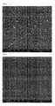
FIG. 2 illustrates a surface image of a substrate having a mixed pattern according to an embodiment of the present invention; -
FIG. 3 illustrates a surface image of a substrate having a dense pattern according to another embodiment of the present invention; -
FIG. 4 illustrates a surface image of a substrate having a coarse pattern according to still another embodiment of the present invention; -
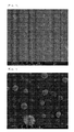
FIG. 5 illustrates a surface image of a substrate having a coating layer with a grain structure, in lieu of a pattern, according to a comparative embodiment of the present invention; -
FIG. 6 illustrates a surface image of a substrate having a coating layer with a network structure, in lieu of a pattern, according to another comparative embodiment of the present invention; and -
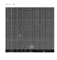
FIG. 7 illustrates a surface image of a substrate having a uniformly deposited coating layer according to still another comparative embodiment of the present invention. - The terms used in the present invention are possibly selected from among currently well-known terms while taking into consideration functions in the present invention, but may vary depending on the cases or intentions of those skilled in the art or on the advent of new technology. Furthermore, some of the terms mentioned in the description of the present invention have been selected by the applicant, the detailed meanings of which should be understood not simply by the actual terms used but by the meaning of each term in the detailed description of the invention or in consideration of the meanings used.
- Hereinafter, a detailed description will be given of the technical construction of the present invention with reference to the appended drawings and the preferred embodiments.
- However, the present invention is not limited to such embodiments and may be modified variously in many different forms. Throughout the specification, the same reference numerals are used to designate the same elements.
- Unlike formation of a uniform coating layer on a substrate using sputtering, the present invention is technically characterized in that a fine pattern is formed by controlling process conditions upon sputtering. In particular, at least one of power and bias conditions is controlled in the present invention.
- According to the present invention, a method of forming a fine pattern using sputtering comprises: preparing a substrate; and sputtering a target material on the substrate to form a pattern, wherein at least one of a power condition and a bias condition is controlled in a predetermined range upon sputtering, thus forming the fine pattern on the substrate.
- Upon sputtering, the power condition is to apply power to the extent that a portion of the target material collides with a pre-deposited target material on the substrate to allow the pre-deposited target material to be separated from the substrate. Hence, the power condition may be differently controlled depending on the kind of target material. Also, the bias condition is to apply bias such that an inert gas in a chamber where the substrate is located collides with the substrate to allow the pre-deposited target material to be separated from the substrate. Hence, the bias condition may be differently controlled depending on the kind of target material.
- As necessary, a temperature condition may be further controlled upon sputtering. Specifically, when the temperature is raised, a coating layer deposited on the surface of the substrate may be softened or reaction activation energy may increase, and thus the etching effect of the coating layer may be enhanced even upon collision of target material particles at the same energy, thereby facilitating the formation of a fine pattern. For control of the temperature condition upon sputtering, the substrate on which the target material is deposited may be heated to 50°C or more. As such, the temperature condition, especially the maximum heating temperature, may vary depending on the kind of target material. Herein, the maximum heating temperature indicates a temperature at which the target material may not be easily applied due to excessive softening of a coating layer having the target material deposited thereon.
- In the present invention, at least one of power, bias and temperature conditions may be controlled upon sputtering, and thereby the size of the resulting fine pattern or the pattern interval may be adjusted.
- Useful in the method of forming the fine pattern according to the present invention, the substrate may include all materials generally used in the art. For example, at least one selected from the group consisting of silicon, glass, a metal and ceramic may be employed, and any material may be selectively utilized depending on the application fields and desired properties.
- Also, the target material, which is applied on the substrate to form a fine pattern, may include all materials generally used in the art. For example, useful is at least one selected from the group consisting of an oxide, a metal and a polymer including Teflon.
-
FIG. 1 schematically illustrates the formation of a fine pattern according to embodiments of the present invention. Upon general sputtering, asubstrate 20 and atarget 30 are provided in achamber 10, and power and bias are applied to thesubstrate 20 and thetarget 30, whereby an inert gas such as argon (Ar) in thechamber 10 may collide with the target, so that a target material (T) is separated from thetarget 30, and the separated target material (T) is deposited on thesubstrate 20. As illustrated inFIG. 1 , however, when the applied power is high, a portion of the target material (T) collides with a pre-deposited target material (T) on the substrate to allow the deposited target material (T) to be separated from the substrate, or is not deposited on the surface of thesubstrate 20 but may bounce out due to its originally high collision energy. Furthermore, when high bias is applied, Ar gas collides with thesubstrate 20 and thus causes the deposited target material (T) to be separated from the substrate. Briefly, the same effect as etching upon photolithography may be exhibited. Ultimately, the fine pattern according to the present invention may be simply formed at low cost by applying high power or bias. As used herein, the term "fine pattern" refers to a nano-sized or micro-sized pattern. - When any one condition of power and bias is applied at a low level, the other condition is applied to be higher, and thereby a desired fine pattern may be formed.
- In the present invention, process conditions are controlled, without the use of existing pattern formation processes including photolithography, mechanical processing, irradiation with X-ray or e-beam, etc., thereby making it possible to simply form the fine pattern at low cost using only sputtering, resulting in superior productivity and economic benefits.
- As used herein, the term "fine pattern" refers to an atypical or random pattern in which at least one of shape and array interval of individual elements of the pattern is different but the individual elements appear to be overall similar to a regular pattern, rather than a pattern in which individual elements are completely regularly arranged and have a predetermined shape.
- In the present invention, the atypical fine pattern is similar to a regular pattern, and also may have advantages that cannot be ensured in a completely regular pattern. This is because the aforementioned process factors are controlled, and thus the fine pattern according to the present invention having an atypical shape may be designed so as to be adapted for desired purposes and end-uses in such a manner that the pattern of the invention may be formed as it is or may be formed to be very similar to a regular pattern. As the process conditions are controlled upon sputtering, a pattern having a large pattern interval and an irregular shape (hereinafter, referred to as a "coarse pattern"), or a pattern having a dense pattern interval and a more regular shape (hereinafter, referred to as a "dense pattern") may be obtained. Alternatively, a structure in which the above patterns are mixed (hereinafter, referred to as a "mixed pattern") may be provided. Since such patterns have different contact angles, they may be employed in processing of a fine pattern for use in electronic devices or bio devices, and especially may be applied to the control of extreme properties including ultra water repellency or ultra hydrophilicity.
- Meanwhile, in the present invention, when the same target material is used, power and/or bias may be applied at a high level compared to general sputtering process conditions. In particular, when a polymer such as Teflon is used as the target material, power is set to 3.46 ∼ 14.81 W/cm2, and bias is set to 0.11 ∼ 0.76 W/cm2. Preferably, power falls in the range of 4.94 ∼ 14.81 W/cm2 and more preferably 4.94 ∼ 9.87 W/cm2. Also, bias is preferably in the range of 0.15 ∼ 0.76 W/cm2 and more preferably 0.15 ∼ 0.38 W/cm2.
- When the target material is a polymer such as Teflon as in the following examples, upon sputtering, the power condition may be 3.46 ∼ 14.81 W/cm2, the bias condition may be 0.11 ∼ 0.76 W/cm2, and the temperature condition may be 50 ∼ 300°C (which is the heating temperature at a position spaced apart by 12 cm from the substrate).
- Specifically, to form a fine pattern on the substrate using Teflon as the target material, power applied to the target preferably falls in the range of 3.46 ∼ 14.81 W/cm2, and bias applied to the substrate is preferably in the range of 0.11 ∼ 0.76 W/cm2. If the power is less than 3.46 W/cm2 or the bias is less than 0.11 W/cm2, when the target material is sputtered on the substrate, energy applied to the target material is low, and thus the target material may be uniformly applied on the substrate as in a general sputtering process, making it difficult to form the pattern.
- In contrast, if the power exceeds 14.81 W/cm2 or the bias exceeds 0.76 W/cm2, energy of the target material is too high, and thus deposition may not be easily carried out on the substrate, making it impossible to form the pattern.
- According to the present invention, a fine pattern may be formed under control of the temperature, without applying the bias. More specifically, the power applied to the target is set to 3.46 ∼ 14.81 W/cm2, and simultaneously, heating is performed so that the temperature is in the range of 50 ∼ 300°C. If the temperature is lower than 50°C, the coating layer may not be effectively softened, making it difficult to form the fine pattern. In contrast, if the temperature is higher than 300°C, the coating process with the target material may not be easy due to excessive softening of the coating layer. Hence, the temperature is preferably set to the range of 50 ∼ 300°C, and more preferably 100 ∼ 300°C for energy enhancement effects. Much more preferably, the temperature is set to 150 ∼ 250°C taking into consideration the target material weak to high temperature, such as a polymer.
- In the present invention, heating for controlling the temperature condition may be conducted at a position by a predetermined distance from the substrate due to the nature of an apparatus for use in the method of the invention, and this distance may vary as necessary or may be set differently depending on the kind of apparatus. In the following examples, heating was performed at a position spaced apart by about 12 cm from the substrate. Furthermore, heating may be conducted at a position shorter or longer from the substrate, or may be implemented directly under the substrate. In this case, heating may be carried out in the temperature range different from the heating temperature range disclosed in the examples of the present invention based on 12 cm, which may be incorporated in the scope of the present invention. Even when the substrate is heated in the corresponding temperature range, the temperature near the substrate is much lower than the heating temperature due to almost vacuum-like atmosphere in the chamber. Furthermore, the temperature near the substrate may become similar to the temperature level increasing in proportion to application of the power or bias.
- Upon sputtering for forming a fine pattern as disclosed in the following examples, a distance between the substrate and the target is preferably set to 3 ∼ 7 cm. If the distance is less than 3 cm, excessive energy is supplied to the target material due to the very short distance between the substrate and the target, making it difficult to form the fine pattern. In contrast, if the distance is greater than 7 cm, too low energy is applied to the target material and thus the pattern cannot be formed. More preferably, the distance between the substrate and the target is set to 4 ∼ 6 cm.
- Also, the pressure in the chamber where sputtering is performed in the following examples is preferably set to 1 ∼ 7 mTorr under general experimental conditions. The pressure in the chamber is related to collision energy of target material particles. As the pressure approximates to high vacuum, interference between the target material particles colliding with the substrate may decrease in terms of mean free path, and thus collision energy of the target material particles may increase, making it easy to form the pattern. For such effects, the pressure in the chamber is preferably set to 7 mTorr or less. If the pressure in the chamber is less than 1 mTorr, an excessive vacuum atmosphere may be formed, thus making it difficult to perform sputtering. However, when specific experimental conditions are given without the use of inert gas in the chamber, instead of general experimental conditions, sputtering is possible even at a pressure in the chamber of less than 1 mTorr.
- As mentioned above, the method of the invention enables the simple formation of a fine pattern at low cost. Moreover, the fine pattern of the invention may be water-repellent and may thus be effectively applied to products requiring water repellency. Furthermore, the magnitude of water repellency may be appropriately controlled by adjusting the shape of the fine pattern and by changing the kind of coating material. As used herein, the term "water repellency" refers to a contact angle with water of 100° or more.
- Meanwhile, in the present invention, forming a water-repellent coating layer may be further carried out either or both of before and after forming the fine pattern, thereby further enhancing water repellency. A general water-repellent coating layer has a contact angle of about 110°, and the fine pattern of the invention has water repellency similar to or superior to the general water-repellent coating layer. Accordingly, when the water-repellent coating layer is formed either or both of before and after forming the fine pattern, it is possible to prepare a substrate having a coating layer having a contact angle of 130 ∼ 150°, and thus such a substrate is preferably applied to products requiring ultra water repellency. Forming the water-repellent coating layer is not particularly limited in the present invention, and may be performed using any material or process widely known in the art.
- A better understanding of the present invention may be obtained via the following examples which are set forth to illustrate, but are not to be construed as limiting the scope of the present invention.
- A silicon substrate and a 2-inch Teflon target having a circular disk shape were prepared, and the silicone substrate was coated with the target material for 60 min using a sputtering apparatus under sputtering conditions as shown in Table 1 below. Then, Ar gas was allowed to flow in the chamber. In the following table, the distance indicates a distance between the substrate and the target, the heating temperature is a temperature applied toward the substrate at a position spaced apart by 12 cm from the substrate, and the measurement temperature is a temperature measured at a position spaced apart by 4 ∼ 6 cm from the substrate. Ultimately, fine pattern-formed substrates 1 to 3 resulting from coating the substrate with the target material were obtained.
[Table 1] Class. Power (W/cm2) Bias (W/cm2) Distance (cm) Pressure in chamber (mTorr) Gas flow rate (SCCM) Heating temp. (°C) Measurement temp. (°C) Ex.1 7.40 0.19 5 2.5 10 300 70.3 Ex.2 7.40 0 5 5 5 300 56.7 Ex.3 7.40 0.19 5 5 5 - 60.2 - Comparative substrates 1 to 9 were obtained in the same manner as in Example 1, with the exception that sputtering conditions as shown in Table 2 below were applied.
[Table 2] Class. Power (W/cm2) Bias (W/cm2) Distance (cm) Pressure in chamber (mTorr) Gas flow rate (SCCM) Heating temp. (°C) Measurement temp. (°C) C.Ex.1 2.47 0 5 2.5 5 - 28.6 C.Ex.2 2.47 0.19 5 2.5 5 300 70.2 C.Ex.3 2.47 0.19 7 5 5 300 66.2 C.Ex.4 2.47 0 7 5 5 - 29.2 C.Ex.5 2.47 0.19 5 5 10 - 46.3 C.Ex.6 7.40 0 5 2.5 10 - 40.4 C.Ex.7 2.47 0 7 2.5 10 300 50.5 C.Ex.8 7.40 0 7 5 10 - 40.2 C.Ex.9 2.47 0 5 5 10 300 45.3 C.Ex.10 2.47 0.19 7 2.5 10 - 46.8 - The surfaces of the fine pattern-formed substrates 1 to 3 obtained in Examples 1 to 3 were observed. The results are shown in
FIGS. 2 to 4 . Also, the surfaces of the comparative substrates 1 to 10 obtained in Comparative Examples 1 to 10 were observed. The results are shown inFIGS. 5 to 7 . - As shown in
FIGS. 2 to 4 , the fine pattern-formed substrates 1 to 3 obtained in Examples 1 to 3 under the sputtering conditions according to the present invention had a fine pattern. -
FIG. 2 illustrates the surface of the fine pattern-formed substrate 1 obtained in Example 1. As illustrated inFIG. 2 , in Example 1 where all of power, bias and heating among the process conditions according to the present invention were applied appropriately, a mixed pattern including a large atypical pattern and a small circular-like pattern, which are combined properly, was formed. -
FIG. 3 illustrates the surface of the fine pattern-formed substrate 2 obtained in Example 2. As illustrated inFIG. 3 , in Example 2 where power and heating among the process conditions according to the present invention were applied appropriately, a dense pattern having a circular-like shape and a narrow pattern interval was formed. -
FIG. 4 illustrates the surface of the fine pattern-formed substrate 3 obtained in Example 3. As illustrated inFIG. 4 , in Example 3 where power and bias among the process conditions according to the present invention were applied appropriately, an atypical coarse pattern, the shape of which is not relatively specific but overall shows a predetermined pattern, was formed compared to Example 2. The pattern interval can also be seen to be large. - On the other hand, in Comparative Examples 1 to 10 in which sputtering was performed under conditions that do not satisfy the process conditions according to the present invention, a coating layer having an irregular grain structure or network structure or a uniform coating layer as in general sputtering was formed, rather than the fine pattern of Examples 1 to 3 according to the present invention.
-
FIG. 5 illustrates the surface of the comparative substrate 1 obtained in Comparative Example 1. As illustrated inFIG. 5 , in Comparative Example 1 where power was applied to be lower than the power range according to the present invention and bias and heating were not applied, the resulting coating layer was configured such that small grains were distributed and large grains were very irregularly formed on a certain portion. - Although not shown, in Comparative Example 2 where power was applied to be lower than the power range according to the present invention and bias and heating were applied, and in Comparative Example 5 where power was applied to be lower than the power range according to the present invention and only bias was applied, almost the same coating layer as in Comparative Example 1 was obtained.
-
FIG. 6 illustrates the surface of the comparative substrate 4 obtained in Comparative Example 4. As illustrated inFIG. 6 , in Comparative Example 4 where power was applied to be lower than the power range according to the present invention and bias and heating were not applied and in which the distance between the substrate and the target was longer than in Comparative Example 1, the resulting coating layer was configured such that comparatively large grains were very irregularly formed and supported by a matrix having a network structure. -
FIG. 7 illustrates the surface of the comparative substrate 6 obtained in Comparative Example 6. As illustrated inFIG. 7 , in Comparative Example 6 where power was applied so as to satisfy the power condition according to the present invention but bias and heating were not applied, a uniform coating layer as in general sputtering was formed. - Although not shown, in Comparative Examples 3, 7 and 10 where bias and heating were applied so as to satisfy the conditions according to the present invention but power was applied at a lower level, the resulting
comparative substrates 3, 7 and 10 had no fine pattern and had a uniform coating layer as in general sputtering. Also, in Comparative Example 8 where power was applied so as to satisfy the power condition according to the present invention but bias and heating were not applied, a uniform coating layer as in general sputtering was formed, like Comparative Example 6. - The water contact angle of the fine pattern-formed substrates 1 to 3 obtained in Examples 1 to 3 was measured. The results are shown in Table 3 below.
[Table 3] Class. Contact angle (°) Ex. 1 116 Ex. 2 109 Ex. 3 106 - As is apparent from Table 3, the fine pattern-formed substrate 1 obtained in Example 1 had a contact angle as large as 116°, and thus exhibited superior water repellency. Further, since the fine pattern-formed substrate 2 obtained in Example 2 had a contact angle of 109°, superior water repellency was obtained. Furthermore, the fine pattern-formed substrate 3 obtained in Example 3 had a contact angle of 106°, resulting in superior water repellency.
- Although the preferred embodiments of the present invention have been disclosed for illustrative purposes, those skilled in the art will appreciate that various modifications and substitutions are possible, without departing from the scope and spirit of the invention as disclosed in the accompanying claims.
Claims (12)
- A method of forming a fine pattern using sputtering, comprising:preparing a substrate; andsputtering a target material on the substrate, thus forming a pattern,wherein upon sputtering, at least one process condition of a power condition in which a portion of the target material collides with a pre-deposited target material on the substrate to allow the pre-deposited target material to be separated from the substrate and a bias condition in which an inert gas in a chamber collides with the substrate to allow the pre-deposited target material to be separated from the substrate is controlled, so that the fine pattern is formed on the substrate.
- The method of claim 1, wherein the substrate comprises at least one selected from the group consisting of silicon, glass, a metal and ceramic.
- The method of claim 1, wherein the target material comprises at least one selected from the group consisting of an oxide, a metal and a polymer.
- The method of claim 1, wherein the process condition further comprises a temperature condition for heating the substrate to 50°C or more.
- The method of claim 4, wherein the temperature condition has a heating temperature of 100 ∼ 300°C at a position spaced apart by 12 cm from the substrate when the target material is a polymer.
- The method of claim 1, wherein when the target material is a polymer, the power condition has a power of 3.46 ∼ 14.81 W/cm2.
- The method of claim 1, wherein when the target material is a polymer, the bias condition has a bias of 0.11 ∼ 0.76 W/cm2.
- The method of claim 1, wherein when the target material is a polymer, a distance between the substrate and a target upon sputtering is 3 ∼ 7 cm.
- The method of claim 1, wherein when the target material is a polymer, a pressure in the chamber upon sputtering is 1 ∼ 7 mTorr.
- The method of claim 1, further comprising forming a water-repellent coating layer on the substrate, before or after forming the pattern.
- A fine pattern formed by the method of any one of claims 1 to 10.
- The fine pattern of claim 11, wherein at least one of shape and array interval of individual elements of the fine pattern is different.
Applications Claiming Priority (2)
| Application Number | Priority Date | Filing Date | Title |
|---|---|---|---|
| KR1020120107946A KR101375878B1 (en) | 2012-09-27 | 2012-09-27 | Method for forming fine pattern |
| PCT/KR2013/008634 WO2014051355A1 (en) | 2012-09-27 | 2013-09-26 | Method for forming fine pattern, and fine pattern formed using same |
Publications (3)
| Publication Number | Publication Date |
|---|---|
| EP2903018A1 true EP2903018A1 (en) | 2015-08-05 |
| EP2903018A4 EP2903018A4 (en) | 2016-05-18 |
| EP2903018B1 EP2903018B1 (en) | 2021-11-24 |
Family
ID=50388649
Family Applications (1)
| Application Number | Title | Priority Date | Filing Date |
|---|---|---|---|
| EP13841594.8A Active EP2903018B1 (en) | 2012-09-27 | 2013-09-26 | Method for forming fine pattern |
Country Status (4)
| Country | Link |
|---|---|
| US (1) | US9637815B2 (en) |
| EP (1) | EP2903018B1 (en) |
| KR (1) | KR101375878B1 (en) |
| WO (1) | WO2014051355A1 (en) |
Families Citing this family (2)
| Publication number | Priority date | Publication date | Assignee | Title |
|---|---|---|---|---|
| KR102311423B1 (en) * | 2016-10-31 | 2021-10-12 | 한국생산기술연구원 | Hard PTFE coating layer |
| KR101914573B1 (en) * | 2016-10-31 | 2018-11-02 | 한국생산기술연구원 | Hard PTFE coating layer and Hard PTFE coating method |
Family Cites Families (6)
| Publication number | Priority date | Publication date | Assignee | Title |
|---|---|---|---|---|
| EP0731490A3 (en) * | 1995-03-02 | 1998-03-11 | Ebara Corporation | Ultra-fine microfabrication method using an energy beam |
| US6679976B2 (en) * | 2001-03-16 | 2004-01-20 | 4Wave, Inc. | System and method for performing sputter deposition with multiple targets using independent ion and electron sources and independent target biasing with DC pulse signals |
| US7378356B2 (en) * | 2002-03-16 | 2008-05-27 | Springworks, Llc | Biased pulse DC reactive sputtering of oxide films |
| US7842605B1 (en) | 2003-04-11 | 2010-11-30 | Novellus Systems, Inc. | Atomic layer profiling of diffusion barrier and metal seed layers |
| JP2005254637A (en) | 2004-03-12 | 2005-09-22 | Casio Comput Co Ltd | Water-repellent structure and manufacturing method thereof |
| KR101272009B1 (en) * | 2008-12-26 | 2013-06-05 | 캐논 아네르바 가부시키가이샤 | Sputtering equipment, sputtering method and method for manufacturing an electronic device |
-
2012
- 2012-09-27 KR KR1020120107946A patent/KR101375878B1/en active Active
-
2013
- 2013-09-26 WO PCT/KR2013/008634 patent/WO2014051355A1/en not_active Ceased
- 2013-09-26 US US14/431,645 patent/US9637815B2/en not_active Expired - Fee Related
- 2013-09-26 EP EP13841594.8A patent/EP2903018B1/en active Active
Also Published As
| Publication number | Publication date |
|---|---|
| US9637815B2 (en) | 2017-05-02 |
| EP2903018A4 (en) | 2016-05-18 |
| US20150259778A1 (en) | 2015-09-17 |
| EP2903018B1 (en) | 2021-11-24 |
| KR101375878B1 (en) | 2014-03-17 |
| WO2014051355A1 (en) | 2014-04-03 |
Similar Documents
| Publication | Publication Date | Title |
|---|---|---|
| KR102842735B1 (en) | Nanoparticle manufacturing | |
| KR100958480B1 (en) | Organic EL display and manufacturing method thereof | |
| CN111943130B (en) | Nano needle array and preparation method and application thereof | |
| TWI510428B (en) | Transparent conductive articles | |
| TW201029950A (en) | Sintered complex oxide and sputtering target comprising same | |
| JP2010516892A (en) | High density refractory metal and alloy sputtering targets | |
| TWI496758B (en) | In-Ga-O-based oxide sintered body, target material, oxide semiconductor thin film, and the like | |
| TW200533764A (en) | Textured-grain-powder metallurgy tantalum sputter target | |
| EP2903018B1 (en) | Method for forming fine pattern | |
| JP2016139688A (en) | Method for manufacturing conductive pattern substrate | |
| CN109314033B (en) | Component for plasma equipment composed of tungsten carbide block | |
| CN102051497B (en) | Preparation methods of gold and silver embedded target and film thereof | |
| CN103320753B (en) | The preparation method of the controlled aluminum nanoparticles array of a kind of size density | |
| Savaloni et al. | Fabrication, characterization and some applications of graded chiral zigzag shaped nano-sculptured silver thin films | |
| CN113631370B (en) | Metallized film and method for producing same | |
| Smith et al. | Growth of ZnO nanowire arrays directly onto Si via substrate topographical adjustments using both wet chemical and dry etching methods | |
| EP2535311B1 (en) | Particle and method for manufacturing same | |
| KR101475133B1 (en) | Sb-Te ALLOY POWDER FOR SINTERING, PROCESS FOR PRODUCTION OF THE POWDER, AND SINTERED TARGET | |
| CN105452529B (en) | The anti-plasma member that aerosol application method and this method are formed | |
| KR20220128184A (en) | Apparatus for pre-oxided porous metal thin film, method for manufacturing porous metal oxide thin film and porous metal oxide thin film manufactured thereby | |
| JP2020180031A (en) | Method for manufacturing glass molding die | |
| CN112687801B (en) | IV-VI semiconductor film and preparation method thereof | |
| TWI353388B (en) | Method for preparing titanium dioxide | |
| WO1992012274A1 (en) | Method of forming oxide film | |
| Yasukawa et al. | Control of the spatial distribution and crystal orientation of self-organized Au nanoparticles |
Legal Events
| Date | Code | Title | Description |
|---|---|---|---|
| PUAI | Public reference made under article 153(3) epc to a published international application that has entered the european phase |
Free format text: ORIGINAL CODE: 0009012 |
|
| 17P | Request for examination filed |
Effective date: 20150416 |
|
| AK | Designated contracting states |
Kind code of ref document: A1 Designated state(s): AL AT BE BG CH CY CZ DE DK EE ES FI FR GB GR HR HU IE IS IT LI LT LU LV MC MK MT NL NO PL PT RO RS SE SI SK SM TR |
|
| AX | Request for extension of the european patent |
Extension state: BA ME |
|
| DAX | Request for extension of the european patent (deleted) | ||
| RA4 | Supplementary search report drawn up and despatched (corrected) |
Effective date: 20160418 |
|
| RIC1 | Information provided on ipc code assigned before grant |
Ipc: C23C 14/12 20060101ALI20160412BHEP Ipc: H01L 21/203 20060101AFI20160412BHEP Ipc: C23C 14/34 20060101ALI20160412BHEP |
|
| STAA | Information on the status of an ep patent application or granted ep patent |
Free format text: STATUS: EXAMINATION IS IN PROGRESS |
|
| 17Q | First examination report despatched |
Effective date: 20180806 |
|
| RIC1 | Information provided on ipc code assigned before grant |
Ipc: H01L 21/203 20060101AFI20210526BHEP Ipc: C23C 14/34 20060101ALI20210526BHEP Ipc: C23C 14/12 20060101ALI20210526BHEP Ipc: C23C 14/04 20060101ALI20210526BHEP |
|
| GRAP | Despatch of communication of intention to grant a patent |
Free format text: ORIGINAL CODE: EPIDOSNIGR1 |
|
| STAA | Information on the status of an ep patent application or granted ep patent |
Free format text: STATUS: GRANT OF PATENT IS INTENDED |
|
| INTG | Intention to grant announced |
Effective date: 20210804 |
|
| GRAS | Grant fee paid |
Free format text: ORIGINAL CODE: EPIDOSNIGR3 |
|
| GRAA | (expected) grant |
Free format text: ORIGINAL CODE: 0009210 |
|
| STAA | Information on the status of an ep patent application or granted ep patent |
Free format text: STATUS: THE PATENT HAS BEEN GRANTED |
|
| AK | Designated contracting states |
Kind code of ref document: B1 Designated state(s): AL AT BE BG CH CY CZ DE DK EE ES FI FR GB GR HR HU IE IS IT LI LT LU LV MC MK MT NL NO PL PT RO RS SE SI SK SM TR |
|
| REG | Reference to a national code |
Ref country code: GB Ref legal event code: FG4D |
|
| REG | Reference to a national code |
Ref country code: AT Ref legal event code: REF Ref document number: 1450498 Country of ref document: AT Kind code of ref document: T Effective date: 20211215 |
|
| REG | Reference to a national code |
Ref country code: DE Ref legal event code: R096 Ref document number: 602013080211 Country of ref document: DE |
|
| REG | Reference to a national code |
Ref country code: IE Ref legal event code: FG4D |
|
| REG | Reference to a national code |
Ref country code: LT Ref legal event code: MG9D |
|
| REG | Reference to a national code |
Ref country code: NL Ref legal event code: MP Effective date: 20211124 |
|
| REG | Reference to a national code |
Ref country code: AT Ref legal event code: MK05 Ref document number: 1450498 Country of ref document: AT Kind code of ref document: T Effective date: 20211124 |
|
| PG25 | Lapsed in a contracting state [announced via postgrant information from national office to epo] |
Ref country code: RS Free format text: LAPSE BECAUSE OF FAILURE TO SUBMIT A TRANSLATION OF THE DESCRIPTION OR TO PAY THE FEE WITHIN THE PRESCRIBED TIME-LIMIT Effective date: 20211124 Ref country code: LT Free format text: LAPSE BECAUSE OF FAILURE TO SUBMIT A TRANSLATION OF THE DESCRIPTION OR TO PAY THE FEE WITHIN THE PRESCRIBED TIME-LIMIT Effective date: 20211124 Ref country code: FI Free format text: LAPSE BECAUSE OF FAILURE TO SUBMIT A TRANSLATION OF THE DESCRIPTION OR TO PAY THE FEE WITHIN THE PRESCRIBED TIME-LIMIT Effective date: 20211124 Ref country code: BG Free format text: LAPSE BECAUSE OF FAILURE TO SUBMIT A TRANSLATION OF THE DESCRIPTION OR TO PAY THE FEE WITHIN THE PRESCRIBED TIME-LIMIT Effective date: 20220224 Ref country code: AT Free format text: LAPSE BECAUSE OF FAILURE TO SUBMIT A TRANSLATION OF THE DESCRIPTION OR TO PAY THE FEE WITHIN THE PRESCRIBED TIME-LIMIT Effective date: 20211124 |
|
| PG25 | Lapsed in a contracting state [announced via postgrant information from national office to epo] |
Ref country code: IS Free format text: LAPSE BECAUSE OF FAILURE TO SUBMIT A TRANSLATION OF THE DESCRIPTION OR TO PAY THE FEE WITHIN THE PRESCRIBED TIME-LIMIT Effective date: 20220324 Ref country code: SE Free format text: LAPSE BECAUSE OF FAILURE TO SUBMIT A TRANSLATION OF THE DESCRIPTION OR TO PAY THE FEE WITHIN THE PRESCRIBED TIME-LIMIT Effective date: 20211124 Ref country code: PT Free format text: LAPSE BECAUSE OF FAILURE TO SUBMIT A TRANSLATION OF THE DESCRIPTION OR TO PAY THE FEE WITHIN THE PRESCRIBED TIME-LIMIT Effective date: 20220324 Ref country code: PL Free format text: LAPSE BECAUSE OF FAILURE TO SUBMIT A TRANSLATION OF THE DESCRIPTION OR TO PAY THE FEE WITHIN THE PRESCRIBED TIME-LIMIT Effective date: 20211124 Ref country code: NO Free format text: LAPSE BECAUSE OF FAILURE TO SUBMIT A TRANSLATION OF THE DESCRIPTION OR TO PAY THE FEE WITHIN THE PRESCRIBED TIME-LIMIT Effective date: 20220224 Ref country code: NL Free format text: LAPSE BECAUSE OF FAILURE TO SUBMIT A TRANSLATION OF THE DESCRIPTION OR TO PAY THE FEE WITHIN THE PRESCRIBED TIME-LIMIT Effective date: 20211124 Ref country code: LV Free format text: LAPSE BECAUSE OF FAILURE TO SUBMIT A TRANSLATION OF THE DESCRIPTION OR TO PAY THE FEE WITHIN THE PRESCRIBED TIME-LIMIT Effective date: 20211124 Ref country code: HR Free format text: LAPSE BECAUSE OF FAILURE TO SUBMIT A TRANSLATION OF THE DESCRIPTION OR TO PAY THE FEE WITHIN THE PRESCRIBED TIME-LIMIT Effective date: 20211124 Ref country code: GR Free format text: LAPSE BECAUSE OF FAILURE TO SUBMIT A TRANSLATION OF THE DESCRIPTION OR TO PAY THE FEE WITHIN THE PRESCRIBED TIME-LIMIT Effective date: 20220225 Ref country code: ES Free format text: LAPSE BECAUSE OF FAILURE TO SUBMIT A TRANSLATION OF THE DESCRIPTION OR TO PAY THE FEE WITHIN THE PRESCRIBED TIME-LIMIT Effective date: 20211124 |
|
| PG25 | Lapsed in a contracting state [announced via postgrant information from national office to epo] |
Ref country code: SM Free format text: LAPSE BECAUSE OF FAILURE TO SUBMIT A TRANSLATION OF THE DESCRIPTION OR TO PAY THE FEE WITHIN THE PRESCRIBED TIME-LIMIT Effective date: 20211124 Ref country code: SK Free format text: LAPSE BECAUSE OF FAILURE TO SUBMIT A TRANSLATION OF THE DESCRIPTION OR TO PAY THE FEE WITHIN THE PRESCRIBED TIME-LIMIT Effective date: 20211124 Ref country code: RO Free format text: LAPSE BECAUSE OF FAILURE TO SUBMIT A TRANSLATION OF THE DESCRIPTION OR TO PAY THE FEE WITHIN THE PRESCRIBED TIME-LIMIT Effective date: 20211124 Ref country code: EE Free format text: LAPSE BECAUSE OF FAILURE TO SUBMIT A TRANSLATION OF THE DESCRIPTION OR TO PAY THE FEE WITHIN THE PRESCRIBED TIME-LIMIT Effective date: 20211124 Ref country code: DK Free format text: LAPSE BECAUSE OF FAILURE TO SUBMIT A TRANSLATION OF THE DESCRIPTION OR TO PAY THE FEE WITHIN THE PRESCRIBED TIME-LIMIT Effective date: 20211124 Ref country code: CZ Free format text: LAPSE BECAUSE OF FAILURE TO SUBMIT A TRANSLATION OF THE DESCRIPTION OR TO PAY THE FEE WITHIN THE PRESCRIBED TIME-LIMIT Effective date: 20211124 |
|
| REG | Reference to a national code |
Ref country code: DE Ref legal event code: R097 Ref document number: 602013080211 Country of ref document: DE |
|
| PLBE | No opposition filed within time limit |
Free format text: ORIGINAL CODE: 0009261 |
|
| STAA | Information on the status of an ep patent application or granted ep patent |
Free format text: STATUS: NO OPPOSITION FILED WITHIN TIME LIMIT |
|
| PG25 | Lapsed in a contracting state [announced via postgrant information from national office to epo] |
Ref country code: AL Free format text: LAPSE BECAUSE OF FAILURE TO SUBMIT A TRANSLATION OF THE DESCRIPTION OR TO PAY THE FEE WITHIN THE PRESCRIBED TIME-LIMIT Effective date: 20211124 |
|
| 26N | No opposition filed |
Effective date: 20220825 |
|
| PG25 | Lapsed in a contracting state [announced via postgrant information from national office to epo] |
Ref country code: SI Free format text: LAPSE BECAUSE OF FAILURE TO SUBMIT A TRANSLATION OF THE DESCRIPTION OR TO PAY THE FEE WITHIN THE PRESCRIBED TIME-LIMIT Effective date: 20211124 |
|
| REG | Reference to a national code |
Ref country code: DE Ref legal event code: R119 Ref document number: 602013080211 Country of ref document: DE |
|
| PG25 | Lapsed in a contracting state [announced via postgrant information from national office to epo] |
Ref country code: MC Free format text: LAPSE BECAUSE OF FAILURE TO SUBMIT A TRANSLATION OF THE DESCRIPTION OR TO PAY THE FEE WITHIN THE PRESCRIBED TIME-LIMIT Effective date: 20211124 |
|
| REG | Reference to a national code |
Ref country code: CH Ref legal event code: PL |
|
| REG | Reference to a national code |
Ref country code: BE Ref legal event code: MM Effective date: 20220930 |
|
| PG25 | Lapsed in a contracting state [announced via postgrant information from national office to epo] |
Ref country code: IT Free format text: LAPSE BECAUSE OF FAILURE TO SUBMIT A TRANSLATION OF THE DESCRIPTION OR TO PAY THE FEE WITHIN THE PRESCRIBED TIME-LIMIT Effective date: 20211124 |
|
| PG25 | Lapsed in a contracting state [announced via postgrant information from national office to epo] |
Ref country code: LU Free format text: LAPSE BECAUSE OF NON-PAYMENT OF DUE FEES Effective date: 20220926 |
|
| PG25 | Lapsed in a contracting state [announced via postgrant information from national office to epo] |
Ref country code: LI Free format text: LAPSE BECAUSE OF NON-PAYMENT OF DUE FEES Effective date: 20220930 Ref country code: IE Free format text: LAPSE BECAUSE OF NON-PAYMENT OF DUE FEES Effective date: 20220926 Ref country code: FR Free format text: LAPSE BECAUSE OF NON-PAYMENT OF DUE FEES Effective date: 20220930 Ref country code: DE Free format text: LAPSE BECAUSE OF NON-PAYMENT OF DUE FEES Effective date: 20230401 Ref country code: CH Free format text: LAPSE BECAUSE OF NON-PAYMENT OF DUE FEES Effective date: 20220930 |
|
| PG25 | Lapsed in a contracting state [announced via postgrant information from national office to epo] |
Ref country code: BE Free format text: LAPSE BECAUSE OF NON-PAYMENT OF DUE FEES Effective date: 20220930 |
|
| PG25 | Lapsed in a contracting state [announced via postgrant information from national office to epo] |
Ref country code: HU Free format text: LAPSE BECAUSE OF FAILURE TO SUBMIT A TRANSLATION OF THE DESCRIPTION OR TO PAY THE FEE WITHIN THE PRESCRIBED TIME-LIMIT; INVALID AB INITIO Effective date: 20130926 |
|
| PG25 | Lapsed in a contracting state [announced via postgrant information from national office to epo] |
Ref country code: CY Free format text: LAPSE BECAUSE OF FAILURE TO SUBMIT A TRANSLATION OF THE DESCRIPTION OR TO PAY THE FEE WITHIN THE PRESCRIBED TIME-LIMIT Effective date: 20211124 |
|
| PG25 | Lapsed in a contracting state [announced via postgrant information from national office to epo] |
Ref country code: MK Free format text: LAPSE BECAUSE OF FAILURE TO SUBMIT A TRANSLATION OF THE DESCRIPTION OR TO PAY THE FEE WITHIN THE PRESCRIBED TIME-LIMIT Effective date: 20211124 |
|
| PG25 | Lapsed in a contracting state [announced via postgrant information from national office to epo] |
Ref country code: TR Free format text: LAPSE BECAUSE OF FAILURE TO SUBMIT A TRANSLATION OF THE DESCRIPTION OR TO PAY THE FEE WITHIN THE PRESCRIBED TIME-LIMIT Effective date: 20211124 |
|
| PG25 | Lapsed in a contracting state [announced via postgrant information from national office to epo] |
Ref country code: MT Free format text: LAPSE BECAUSE OF FAILURE TO SUBMIT A TRANSLATION OF THE DESCRIPTION OR TO PAY THE FEE WITHIN THE PRESCRIBED TIME-LIMIT Effective date: 20211124 |
|
| PGFP | Annual fee paid to national office [announced via postgrant information from national office to epo] |
Ref country code: GB Payment date: 20250707 Year of fee payment: 13 |