EP2898550B1 - Electronic platform comprising an abo3 type crystal and graphene, method for its manufacture and chip comprising the same - Google Patents
Electronic platform comprising an abo3 type crystal and graphene, method for its manufacture and chip comprising the same Download PDFInfo
- Publication number
- EP2898550B1 EP2898550B1 EP13763256.8A EP13763256A EP2898550B1 EP 2898550 B1 EP2898550 B1 EP 2898550B1 EP 13763256 A EP13763256 A EP 13763256A EP 2898550 B1 EP2898550 B1 EP 2898550B1
- Authority
- EP
- European Patent Office
- Prior art keywords
- graphene
- crystal
- layer
- electronic platform
- chip
- Prior art date
- Legal status (The legal status is an assumption and is not a legal conclusion. Google has not performed a legal analysis and makes no representation as to the accuracy of the status listed.)
- Not-in-force
Links
Images



Classifications
-
- H—ELECTRICITY
- H10—SEMICONDUCTOR DEVICES; ELECTRIC SOLID-STATE DEVICES NOT OTHERWISE PROVIDED FOR
- H10N—ELECTRIC SOLID-STATE DEVICES NOT OTHERWISE PROVIDED FOR
- H10N60/00—Superconducting devices
- H10N60/99—Alleged superconductivity
-
- H—ELECTRICITY
- H01—ELECTRIC ELEMENTS
- H01B—CABLES; CONDUCTORS; INSULATORS; SELECTION OF MATERIALS FOR THEIR CONDUCTIVE, INSULATING OR DIELECTRIC PROPERTIES
- H01B1/00—Conductors or conductive bodies characterised by the conductive materials; Selection of materials as conductors
- H01B1/02—Conductors or conductive bodies characterised by the conductive materials; Selection of materials as conductors mainly consisting of metals or alloys
-
- H—ELECTRICITY
- H01—ELECTRIC ELEMENTS
- H01B—CABLES; CONDUCTORS; INSULATORS; SELECTION OF MATERIALS FOR THEIR CONDUCTIVE, INSULATING OR DIELECTRIC PROPERTIES
- H01B1/00—Conductors or conductive bodies characterised by the conductive materials; Selection of materials as conductors
- H01B1/04—Conductors or conductive bodies characterised by the conductive materials; Selection of materials as conductors mainly consisting of carbon-silicon compounds, carbon or silicon
-
- H—ELECTRICITY
- H01—ELECTRIC ELEMENTS
- H01B—CABLES; CONDUCTORS; INSULATORS; SELECTION OF MATERIALS FOR THEIR CONDUCTIVE, INSULATING OR DIELECTRIC PROPERTIES
- H01B12/00—Superconductive or hyperconductive conductors, cables, or transmission lines
- H01B12/02—Superconductive or hyperconductive conductors, cables, or transmission lines characterised by their form
-
- H—ELECTRICITY
- H05—ELECTRIC TECHNIQUES NOT OTHERWISE PROVIDED FOR
- H05K—PRINTED CIRCUITS; CASINGS OR CONSTRUCTIONAL DETAILS OF ELECTRIC APPARATUS; MANUFACTURE OF ASSEMBLAGES OF ELECTRICAL COMPONENTS
- H05K1/00—Printed circuits
- H05K1/02—Details
- H05K1/03—Use of materials for the substrate
- H05K1/0306—Inorganic insulating substrates, e.g. ceramic, glass
-
- H—ELECTRICITY
- H05—ELECTRIC TECHNIQUES NOT OTHERWISE PROVIDED FOR
- H05K—PRINTED CIRCUITS; CASINGS OR CONSTRUCTIONAL DETAILS OF ELECTRIC APPARATUS; MANUFACTURE OF ASSEMBLAGES OF ELECTRICAL COMPONENTS
- H05K1/00—Printed circuits
- H05K1/02—Details
- H05K1/09—Use of materials for the conductive, e.g. metallic pattern
-
- H—ELECTRICITY
- H10—SEMICONDUCTOR DEVICES; ELECTRIC SOLID-STATE DEVICES NOT OTHERWISE PROVIDED FOR
- H10N—ELECTRIC SOLID-STATE DEVICES NOT OTHERWISE PROVIDED FOR
- H10N30/00—Piezoelectric or electrostrictive devices
-
- H—ELECTRICITY
- H10—SEMICONDUCTOR DEVICES; ELECTRIC SOLID-STATE DEVICES NOT OTHERWISE PROVIDED FOR
- H10N—ELECTRIC SOLID-STATE DEVICES NOT OTHERWISE PROVIDED FOR
- H10N60/00—Superconducting devices
- H10N60/10—Junction-based devices
- H10N60/12—Josephson-effect devices
-
- H—ELECTRICITY
- H10—SEMICONDUCTOR DEVICES; ELECTRIC SOLID-STATE DEVICES NOT OTHERWISE PROVIDED FOR
- H10N—ELECTRIC SOLID-STATE DEVICES NOT OTHERWISE PROVIDED FOR
- H10N60/00—Superconducting devices
- H10N60/80—Constructional details
- H10N60/85—Superconducting active materials
- H10N60/855—Ceramic superconductors
-
- Y—GENERAL TAGGING OF NEW TECHNOLOGICAL DEVELOPMENTS; GENERAL TAGGING OF CROSS-SECTIONAL TECHNOLOGIES SPANNING OVER SEVERAL SECTIONS OF THE IPC; TECHNICAL SUBJECTS COVERED BY FORMER USPC CROSS-REFERENCE ART COLLECTIONS [XRACs] AND DIGESTS
- Y10—TECHNICAL SUBJECTS COVERED BY FORMER USPC
- Y10T—TECHNICAL SUBJECTS COVERED BY FORMER US CLASSIFICATION
- Y10T428/00—Stock material or miscellaneous articles
- Y10T428/30—Self-sustaining carbon mass or layer with impregnant or other layer
Definitions
- the present invention relates to electronic and optoelectronic devices showing very low electrical resistance, more in particular, to superconductive devices comprising graphene and ABO 3 crystals.
- suspended graphene as well as graphene on hexagonal boron nitride typically show a conductivity one order of magnitude larger than graphene on glass.
- the improved electrical performance of graphene on crystalline boron nitride is mainly due to a lower surface roughness and the interactions at the interface with the substrate, thanks to the matching of the graphene lattice with the hexagonal boron nitride. It has also been theoretically shown that graphene can become superconductive if properly intercalated by lithium atoms, though with very low (about 10K) critical temperatures [ G. Profeta et al., Nature Physics vol.8, p.131 (2012 )]. In another theoretical work [ G. Savini et al., Phys. Rev.
- the present invention aims to achieve an electronic or optoelectronic platform with sheet resistance lower than 1 ⁇ /square, at higher temperatures as in the prior art, that is, higher than 77K.
- the invention comprises an electronic platform comprising a substrate made of a ABO 3 crystal and at least one layer of a two-dimensional conducting sheet of carbon atoms of a thickness between one and four atoms, wherein the conducting layer are placed on top of a face of the crystal whose orthogonal axis is at an angle up to 35o of the crystal's spontaneous polarization axis (usually called c-axis or c-cut).
- the crystal can be LiNbO 3 LiTaO 3 LilO 3 , Ba x Sr 1-x TiO 3 , Pb(Zr x Ti 1-x )O 3 , with x varying between 0 and 1.
- the graphene layer is shaped as Hall bars and the platform comprises gold contacts of a thickness of 10 to 1000 nm.
- the invention also comprises a chip platform with a layer of chromium of a thickness of 1 to 50 nm between the graphene layer and the gold contacts.
- the invention is based on the following effect:
- the crystal structure of LiNbO 3 consists of distorted oxygen octahedra by sharing their corners, faces and edges along different crystallographic directions, forming a trigonal ( c -axial) lattice.
- the ideal cation stacking sequence along the trigonal axis is ⁇ -Li-Nb- ⁇ -Li-Nb- ⁇ - ⁇ where ⁇ indicates a vacancy
- each octahedron shares its oxygen planes with the neighboring upper and lower ones.
- each octahedron is surrounded by other six octahedra, e.g. each LiO 6 octahedron is surrounded by three ⁇ O 6 octahedra and three NbO 6 octahedra [ D. Xue et al., Journal of Physics and Chemistry of Solids vol.66, p.589 (2005 )].
- LiNbO 3 in its ferroelectric phase has a spontaneous electrical polarization (P s ) of about 0.72 C/m 2 along the c-axis.
- the ferroelectric state is characterised by a hysteresis effect of the electrical polarization as a function of the applied electric field, making the crystal possess P s in the absence of an external electrical field.
- a region of the crystal with uniform P s is called domain.
- the crystal is called single domain or single crystal when it has the same P s through the whole volume.
- LiNbO 3 can also have either a paraelectric phase whereby there are no regions with P s or a multidomain crystal structure consisting of domain regions oriented in a random or predefined manner.
- the side view of the structure of ferroelectric LiNbO 3 is represented in Fig. 2 .
- the Li + ions are positioned on opposite sides of the oxygen planes while the Nb 5+ ions are in between oxygen planes. It is also known that one can switch the spontaneous polarization, e.g. create opposite domain regions or orient all the domains in the same direction (form a single domain structure) by applying high electric fields, of the order of 20kV/mm at room temperature. During this process, named electric-field domain inversion or poling, the Li + ions move across the oxygen planes while the Nb 5+ ions are displaced between two consecutive oxygen planes, and the distances between the atoms change [ X. Zhang et al., Materials Science and Engineering B vol. 120, p. 21 (2005 )]. Fig.
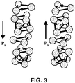
- LiNbO 3 shows the ferroelectric LiNbO 3 structure of oppositely oriented domains (up and down spontaneous polarization).
- LiNbO 3 also possesses pyroelectric, piezoelectric, photorefractive and nonlinear optical properties.
- the pyroelectric effect consists in a change of the spontaneous polarization upon temperature and it is characterised by the pyroelectric coefficient ( p i ) which, for LiNbO 3 , is about -4x10 -5 C/(m 2 K).
- p i depends on temperature as it is shown by Y.V. Shaldinfor for the range below 300K [ Y.V. Shaldin, Crystallography Reports vol.53, p.847 (2008 )].
- the polarization charge change can reach values of 1.44 C/m 2 .
- the piezoelectric effect consists in a change of spontaneous polarization due to application of pressure (stress) for example through a mechanical deformation.
- pressure stress
- polarization charges are induced.
- bound charges are generated which create electric fields. This is always accompanied by the attraction or generation of free charges which compensate (neutralize) the bound charges.
- the speed of the charge compensation (neutralization) depends on the effect and external conditions.
- the process is slow in vacuum in the case of the pyroelectric effect and it is practically instantaneous in the case of domain inversion by applying external electric fields using voltage generators, which also provide the free charges.
- Superconductivity requires strong interactions between charge carriers and lattice vibrations (phonons).
- LiNbO 3 as well as other ferro-electric materials carry optical phonon modes which are strongly coupled to the electronic degree of freedom.
- the lithium ions under temperature changes become very reactive and mobile, thus increasing the chance of intercalation in the graphene. It is reported that in the presence of strong electrical fields, the ABO 3 crystals could show a superconductive behaviour ( K. Ueno et al., Nature Materials vol. 7 page 855 (2008 )).
- ferroelectric ABO 3 crystals possess properties similar to LiNbO 3 and could be used for the purpose of the invention. These include LiTaO 3 LilO 3 , Ba x Sr 1-x TiO 3 , Pb(Zr x Ti 1-x )O 3 , with x varying between 0 and 1.
- An embodiment of the electronic or optoelectronic platform according to the invention can be seen in Figs. 4 to 6 .
- a two-dimensional conductor consisting of a sheet of carbon atoms with a thickness of one to 4 atoms is deposited on a face of a lithium niobate crystal prepared by known means with a face whose orthogonal axis is up to 35o oriented with respect to the c-axis of the crystal
- the fabrication process of the devices starts with the cleaning of the lithium niobate substrates employing well known procedure in semiconductor fabrication both wet (e.g acetone and isopropanol sonication, cleaning in an alkaline soap, NH 4 OH:H 2 O 2 :H 2 O solution) and dry (e.g. plasma cleaning with oxygen).
- graphene can be deposited by known techniques directly on top of the substrate surface either before the electrical contact fabrication or after their deposition.
- One or a plurality of atom thick layers are deposited.
- the fabrication of the contacts is typically made by physical vapor deposition techniques (e.g evaporation, sputtering etc.) by depositing for instance a layer of chromium, titanium or nickel with a thickness ranging from 1 to 50 nm and on top of it a layer of gold having a thickness ranging from 10 to 1000 nm.
- the patterning of graphene to obtain the desired shape e.g.
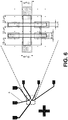
- hall bars with typical dimensions as in fig.6 is carried out by first depositing a very thin layer of a protecting material, typically an aluminum layer ranging from 1 to 20 nm, most commonly 3 nm.
- a protecting material typically an aluminum layer ranging from 1 to 20 nm, most commonly 3 nm.
- the pattern of the device is defined by resist photolithography.
- the photoresist remains on top of the graphene to protect it during the following step.
- the unprotected graphene is etched away in a reactive ion etching oxygen plasma system with techniques well known in the literature and the final shapes of the graphene layer obtained.
- the resist can be left as a protection in the case of graphene on top of the contacts or removed to further proceed with the fabrication.
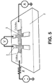
- the chip After the fabrication process the chip is inserted into a cryogenic chamber in vacuum where it is electrically connected according to the scheme in Fig. 5 .
- the external resistance R in the figure is much larger than the resistance of the graphene layer between the two points where the voltage V is measured.
- a four point probe measurement technique can be used as indicated in Fig 5 and it is calculated by dividing the voltage V measured by the voltage probes by the current I.
- An important step in order to obtain a very low resistance device includes a process, e.g. pyroelectric effect, piezoelectric effect, domain inversion, that can induce changes in the spontaneous polarization, thus bound charges in proximity to the crystal's surface and the graphene layer. As a consequence free charges are drawn into the graphene layer which increases their electrical conductivity.
- the process can rely on the pyroelectric effect by a thermal cycling applied in the cryostat.
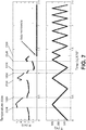
- Fig. 7 it is shown that a proper thermal cycling (bottom) induces jumps in the measured resistance until this reaches stably a value close to zero.
- the cycle consists at least of a decrease of at least 1K/min from room temperature to a temperature below the critical temperature, i.e.
- the cycle can also consists of a number of cycles to induce the low resistance state, with a temperature ranging from a minimum of 1 K to a maximum of 600K, being typically between 10K to 300K.
- the number of cycles needed to induce the low resistance state can range from 1 to 100 with a typical value of 5 while the temperature ramp rate can range from 1K/min to 15K/min being typically 5K/min. Note that after being reached the low resistance state is maintained during subsequent cycles.
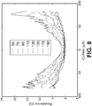
- Fig. 8 shows that the designed platform reached practically zero electrical resistance and the range over which it is maintained close to zero reduces for increasing temperature.
Landscapes
- Engineering & Computer Science (AREA)
- Microelectronics & Electronic Packaging (AREA)
- Chemical & Material Sciences (AREA)
- Ceramic Engineering (AREA)
- Inorganic Chemistry (AREA)
- Crystals, And After-Treatments Of Crystals (AREA)
- Carbon And Carbon Compounds (AREA)
Description
- The present invention relates to electronic and optoelectronic devices showing very low electrical resistance, more in particular, to superconductive devices comprising graphene and ABO3 crystals.
- Recently graphene, a honeycomb bi-dimensional Carbon monolayer (
Fig.1 ), has become a prominent material of research given its unique properties, including mass-less Dirac behavior for the electrons, quantum hall effect, a minimum conductivity even when the carrier density tends to zero, a high electronic mobility independent of the level of doping for a quite large range and a uniform (2.3%) absorption over the full optical spectral range, impermeability against oxygen, water and helium, high elastic strength. Last but not least, it presents the possibility to tune the electronic and optical properties by changing the level of doping through electric fields. Since the preparation of high quality flakes in 2004 using mechanical exfoliation, several electronic and photonic devices have been realized, including high frequency transistors, liquid crystal displays, high efficiency photodetectors, resonating membranes and organic solar cells. The future industrialization of the graphene containing devices significantly depends on the availability of large graphene sheets with high quality on the appropriate substrate. Another crucial aspect for most of the applications is being able to induce doping in graphene and change its electrical and optical properties. For example an undoped graphene layer has a typical sheet resistance of >1000 ohm/square, making the doping necessary for most of the electric and electronic applications. The electrical properties of graphene also depend significantly on the substrate. For example suspended graphene as well as graphene on hexagonal boron nitride typically show a conductivity one order of magnitude larger than graphene on glass. The improved electrical performance of graphene on crystalline boron nitride is mainly due to a lower surface roughness and the interactions at the interface with the substrate, thanks to the matching of the graphene lattice with the hexagonal boron nitride. It has also been theoretically shown that graphene can become superconductive if properly intercalated by lithium atoms, though with very low (about 10K) critical temperatures [G. Profeta et al., Nature Physics vol.8, p.131 (2012)]. In another theoretical work [G. Savini et al., Phys. Rev. Lett. Vol.105, p.037002 (2010)] it has been shown that hydrogenated graphene (graphane) when properly doped with holes at levels higher than 1014 cm-2 can become superconductive at 90K. Supercurrent in graphene (superconducting proximity effect) was observed experimentally at lower level of carrier density when superconducting contacts were used in a Josephson junction configuration [H.B. Heershe et al., Nature 446, p. 56 (2007)]. SAW sensors comprising a lithium niobate substrate with a graphene surface layer are shown known, the substrates being either YZ-cut or Y-cut (V Chivukula et al. 2010 IEEE Int. Ultrason. Symp. Proc., 257-260; V Miseikis et al. Appl. Phys. Lett. 100 (2012) 133105). - The present invention aims to achieve an electronic or optoelectronic platform with sheet resistance lower than 1 Ω/square, at higher temperatures as in the prior art, that is, higher than 77K.
- For this purpose, the invention comprises an electronic platform comprising a substrate made of a ABO3 crystal and at least one layer of a two-dimensional conducting sheet of carbon atoms of a thickness between one and four atoms, wherein the conducting layer are placed on top of a face of the crystal whose orthogonal axis is at an angle up to 35º of the crystal's spontaneous polarization axis (usually called c-axis or c-cut). The crystal can be LiNbO3 LiTaO3 LilO3, BaxSr1-xTiO3, Pb(ZrxTi1-x)O3, with x varying between 0 and 1. Optionally, the graphene layer is shaped as Hall bars and the platform comprises gold contacts of a thickness of 10 to 1000 nm. The invention also comprises a chip platform with a layer of chromium of a thickness of 1 to 50 nm between the graphene layer and the gold contacts.
- To complete the description and in order to provide for a better understanding of the invention, a set of drawings is provided. Said drawings illustrate a preferred embodiment of the invention, which should not be interpreted as restricting the scope of the invention, but just as an example of how the invention can be embodied. The drawings comprise the following figures:
-
Fig. 1 shows the hexagonal structure of graphene with Carbon atoms distance of about 0.142 nm. -
Fig. 2 shows the octahedra linking conditions of constituent atoms of LiNbO3 crystals in the ab crystallographic plane. -
Fig. 3 is a side view of LiNbO3 crystals with opposite spontaneous polarization (Ps). -
Fig. 4 shows a graphene layer on a c-cut LiNbO3 crystal according to the invention. -
Fig. 5 depicts an embodiment of the inventions of the graphene on LiNbO3 chip layout, electrical measurements set up in the cryogenic environment. -
Fig. 6 shows an embodiment of the invention provided with contacts made of gold and the graphene in the shape of Hall bars. -
Fig. 7 is a graph of the temperature cycle inducing anomalously low electrical resistance in the graphene on LiNbO3 -
Fig. 8 is a graph of the resistance as a function of current at different temperatures after the thermal cycle ofFig. 7 . - The invention is based on the following effect: The crystal structure of LiNbO3 consists of distorted oxygen octahedra by sharing their corners, faces and edges along different crystallographic directions, forming a trigonal (c-axial) lattice. Along the c-axis (the ideal cation stacking sequence along the trigonal axis is □-Li-Nb-□-Li-Nb-□-□ where □ indicates a vacancy) each octahedron shares its oxygen planes with the neighboring upper and lower ones. In the ab plane, perpendicular to the c-axis, each octahedron shares its oxygen edges with the neighboring ones (
Fig.2 ). InFig.2 we can see that each octahedron is surrounded by other six octahedra, e.g. each LiO6 octahedron is surrounded by three □O6 octahedra and three NbO6 octahedra [D. Xue et al., Journal of Physics and Chemistry of Solids vol.66, p.589 (2005)]. LiNbO3 in its ferroelectric phase has a spontaneous electrical polarization (Ps) of about 0.72 C/m2 along the c-axis. The ferroelectric state is characterised by a hysteresis effect of the electrical polarization as a function of the applied electric field, making the crystal possess Ps in the absence of an external electrical field. A region of the crystal with uniform Ps is called domain. The crystal is called single domain or single crystal when it has the same Ps through the whole volume. Note that LiNbO3 can also have either a paraelectric phase whereby there are no regions with Ps or a multidomain crystal structure consisting of domain regions oriented in a random or predefined manner. In a simplified picture the side view of the structure of ferroelectric LiNbO3 is represented inFig. 2 . Note that the Li+ ions are positioned on opposite sides of the oxygen planes while the Nb5+ ions are in between oxygen planes. It is also known that one can switch the spontaneous polarization, e.g. create opposite domain regions or orient all the domains in the same direction (form a single domain structure) by applying high electric fields, of the order of 20kV/mm at room temperature. During this process, named electric-field domain inversion or poling, the Li+ ions move across the oxygen planes while the Nb5+ ions are displaced between two consecutive oxygen planes, and the distances between the atoms change [X. Zhang et al., Materials Science and Engineering B vol. 120, p. 21 (2005)].Fig. 3 shows the ferroelectric LiNbO3 structure of oppositely oriented domains (up and down spontaneous polarization). LiNbO3 also possesses pyroelectric, piezoelectric, photorefractive and nonlinear optical properties. The pyroelectric effect consists in a change of the spontaneous polarization upon temperature and it is characterised by the pyroelectric coefficient (pi ) which, for LiNbO3, is about -4x10⁻⁵ C/(m2K). In reality pi depends on temperature as it is shown by Y.V. Shaldinfor for the range below 300K [Y.V. Shaldin, Crystallography Reports vol.53, p.847 (2008)]. When the temperature changes the Li+ and Nb5+ ions move with respect to the oxygen planes. In particular when the temperature decreases the Li+ and Nb5+ ions move further toward the c+ face, i.e. Ps increases and the c+ face becomes more positive while the c- face becomes more negative. The opposite happens when the temperature is increased. The created polarization bound charge induces internal electric fields of about 0.15 kV/(mm K), if the change in temperature is fast enough not to allow free charges to arrive on the surface and thus compensate for the induced polarization charges. Note that the pyroelectric effect produces the largest charge density on the face of the crystal when it is cut such that the face is orthogonal to the c-axis, i.e. the angle between the orthogonal axis to the face and the c-axis is zero. The pyroelectric effect at low temperature (<300K) has been investigated showing that the electric fields induced might generate internal electrical breakdown, thus providing extra free charge and different screening situations for the spontaneous polarization [S.L. Bravina et al., Ferroelectrics vol.298, p.31 (2004)]. When the temperature variation is sufficiently fast and large (e.g. 100K) the internal electric fields due to the pyroelectric effect might reach values close to the coercive field of the crystal, i.e. the field needed to switch the domains (spontaneous polarization). In that case, as it happens for domain inversion by applying external electrical fields, the polarization charge change can reach values of 1.44 C/m2.
The piezoelectric effect consists in a change of spontaneous polarization due to application of pressure (stress) for example through a mechanical deformation. As it is the case of the pyroelectric effect polarization charges are induced.
Note that when the spontaneous polarization changes, be it for example through the pyroelectric, piezoelectric or domain inversion, bound charges are generated which create electric fields. This is always accompanied by the attraction or generation of free charges which compensate (neutralize) the bound charges. The speed of the charge compensation (neutralization) depends on the effect and external conditions. For example the process is slow in vacuum in the case of the pyroelectric effect and it is practically instantaneous in the case of domain inversion by applying external electric fields using voltage generators, which also provide the free charges. Superconductivity requires strong interactions between charge carriers and lattice vibrations (phonons). LiNbO3 as well as other ferro-electric materials carry optical phonon modes which are strongly coupled to the electronic degree of freedom. In addition, the lithium ions under temperature changes become very reactive and mobile, thus increasing the chance of intercalation in the graphene. It is reported that in the presence of strong electrical fields, the ABO3 crystals could show a superconductive behaviour (K. Ueno et al., Nature Materials vol. 7 page 855 (2008)).
Other ferroelectric ABO3 crystals possess properties similar to LiNbO3 and could be used for the purpose of the invention. These include LiTaO3 LilO3, BaxSr1-xTiO3, Pb(ZrxTi1-x)O3, with x varying between 0 and 1.
An embodiment of the electronic or optoelectronic platform according to the invention can be seen inFigs. 4 to 6 . A two-dimensional conductor consisting of a sheet of carbon atoms with a thickness of one to 4 atoms is deposited on a face of a lithium niobate crystal prepared by known means with a face whose orthogonal axis is up to 35º oriented with respect to the c-axis of the crystal The fabrication process of the devices starts with the cleaning of the lithium niobate substrates employing well known procedure in semiconductor fabrication both wet (e.g acetone and isopropanol sonication, cleaning in an alkaline soap, NH4OH:H2O2:H2O solution) and dry (e.g. plasma cleaning with oxygen). After substrate preparation, graphene can be deposited by known techniques directly on top of the substrate surface either before the electrical contact fabrication or after their deposition. One or a plurality of atom thick layers (each between 0.3 and 0.4 nm thick) are deposited. The fabrication of the contacts is typically made by physical vapor deposition techniques (e.g evaporation, sputtering etc.) by depositing for instance a layer of chromium, titanium or nickel with a thickness ranging from 1 to 50 nm and on top of it a layer of gold having a thickness ranging from 10 to 1000 nm. The patterning of graphene to obtain the desired shape, e.g. hall bars with typical dimensions as infig.6 , is carried out by first depositing a very thin layer of a protecting material, typically an aluminum layer ranging from 1 to 20 nm, most commonly 3 nm. After the protective layer deposition, the pattern of the device is defined by resist photolithography. After the development the photoresist remains on top of the graphene to protect it during the following step. The unprotected graphene is etched away in a reactive ion etching oxygen plasma system with techniques well known in the literature and the final shapes of the graphene layer obtained. After this step the resist can be left as a protection in the case of graphene on top of the contacts or removed to further proceed with the fabrication. After the fabrication process the chip is inserted into a cryogenic chamber in vacuum where it is electrically connected according to the scheme inFig. 5 . Note that the external resistance R in the figure is much larger than the resistance of the graphene layer between the two points where the voltage V is measured. The typical value of that resistance is R= 1 Mohm in order to obtain a current of the order of I=1 µA when the generator is set to 1 V. To obtain the resistance value of the graphene a four point probe measurement technique can be used as indicated inFig 5 and it is calculated by dividing the voltage V measured by the voltage probes by the current I. - An important step in order to obtain a very low resistance device includes a process, e.g. pyroelectric effect, piezoelectric effect, domain inversion, that can induce changes in the spontaneous polarization, thus bound charges in proximity to the crystal's surface and the graphene layer. As a consequence free charges are drawn into the graphene layer which increases their electrical conductivity. For example the process can rely on the pyroelectric effect by a thermal cycling applied in the cryostat. In
Fig. 7 it is shown that a proper thermal cycling (bottom) induces jumps in the measured resistance until this reaches stably a value close to zero. The cycle consists at least of a decrease of at least 1K/min from room temperature to a temperature below the critical temperature, i.e. the temperature at which the transition from normal to low electrical resistance state occurs, e.g. about 170-180K in our case. The cycle can also consists of a number of cycles to induce the low resistance state, with a temperature ranging from a minimum of 1 K to a maximum of 600K, being typically between 10K to 300K. The number of cycles needed to induce the low resistance state can range from 1 to 100 with a typical value of 5 while the temperature ramp rate can range from 1K/min to 15K/min being typically 5K/min. Note that after being reached the low resistance state is maintained during subsequent cycles.Fig. 8 shows that the designed platform reached practically zero electrical resistance and the range over which it is maintained close to zero reduces for increasing temperature. At a temperature around 170-180K this range becomes negligible and correspondingly the resistance starts increasing (deviating from zero). The initial resistance before the thermal cycling was about 2kΩ, after the thermal cycle in the low resistance state (below 170-180K) the resistance becomes lower than 50mΩ and in the normal resistance state (above 170-180K) is always less than 20Ω. The latter value corresponds to a level of doping (carrier concentration) in graphene of the order of 10-4 cm-2. - In this text, the term "comprises" and its derivations (such as "comprising", etc.) should not be understood in an excluding sense, that is, these terms should not be interpreted as excluding the possibility that what is described and defined may include further elements, steps, etc.
- On the other hand, the invention is obviously not limited to the specific embodiment(s) described herein, but also encompasses any variations that may be considered by any person skilled in the art (for example, as regards the choice of materials, dimensions, components, configuration, etc.), within the general scope of the invention as defined in the claims.
Claims (6)
- An electronic platform comprising a substrate made of a ABO3 crystal (2) and at least one layer of a two-dimensional conducting sheet of carbon atoms (1) of a thickness between one and four atoms, characterized in that the conducting layer(s) is (are) placed on top of a face of the crystal whose orthogonal axis is at an angle up to 35º of the crystal's spontaneous polarization or c-axis.
- An electronic platform according to claim 1 wherein the substrate is made of at least one of LiNbO3 LiTaO3 LilO3, BaxSr1-xTiO3, Pb(ZrxTi1-x)O3, with x varying between 0 and 1.
- An electronic platform according to claims 1 or 2 wherein the graphene layer is shaped as Hall bars (4).
- A chip comprising the electronic platform according to previous claims and gold contacts (3) of a thickness of 10 to 1000 nm.
- A chip according to claim 4 further comprising a layer of chromium of a thickness of 1 to 50 nm between the graphene layer and the gold contacts.
- A process for fabricating an electronic platform comprising a substrate of a crystal of the form ABO3 and at least one layer of a two-dimensional conducting sheet of carbon atoms (1) of a thickness between one and four atoms, the method comprising the steps of- depositing the conducting layer(s) on top of a face of the crystal whose orthogonal axis is at an angle up to 35º of the crystal's spontaneous polarization or c-axis.- subjecting the graphene and substrate to a process of change of spontaneous polarization.
Applications Claiming Priority (2)
| Application Number | Priority Date | Filing Date | Title |
|---|---|---|---|
| ES201231444A ES2395949B1 (en) | 2012-09-18 | 2012-09-18 | ELECTRONIC PLATFORM THAT INCLUDES A CRYSTAL OF TYPE ABO3 AND GRAPHENE, METHOD FOR MANUFACTURING AND CHIP THAT INCLUDES THE SAME |
| PCT/EP2013/069351 WO2014044702A1 (en) | 2012-09-18 | 2013-09-18 | Electronic platform comprising an abo3 type crystal and graphene, method for its manufacture and chip comprising the same |
Publications (2)
| Publication Number | Publication Date |
|---|---|
| EP2898550A1 EP2898550A1 (en) | 2015-07-29 |
| EP2898550B1 true EP2898550B1 (en) | 2018-02-21 |
Family
ID=47625613
Family Applications (1)
| Application Number | Title | Priority Date | Filing Date |
|---|---|---|---|
| EP13763256.8A Not-in-force EP2898550B1 (en) | 2012-09-18 | 2013-09-18 | Electronic platform comprising an abo3 type crystal and graphene, method for its manufacture and chip comprising the same |
Country Status (4)
| Country | Link |
|---|---|
| US (1) | US9548435B2 (en) |
| EP (1) | EP2898550B1 (en) |
| ES (1) | ES2395949B1 (en) |
| WO (1) | WO2014044702A1 (en) |
Families Citing this family (4)
| Publication number | Priority date | Publication date | Assignee | Title |
|---|---|---|---|---|
| USD788819S1 (en) * | 2015-02-09 | 2017-06-06 | Lg Electronics Inc. | Virtual reality device |
| US10181521B2 (en) | 2017-02-21 | 2019-01-15 | Texas Instruments Incorporated | Graphene heterolayers for electronic applications |
| US9793214B1 (en) | 2017-02-21 | 2017-10-17 | Texas Instruments Incorporated | Heterostructure interconnects for high frequency applications |
| CN109904050B (en) * | 2019-03-13 | 2020-02-21 | 中山大学 | A device structure of ferroelectric material polarization field regulating field emission of two-dimensional atomic crystal and its preparation method and application |
Family Cites Families (5)
| Publication number | Priority date | Publication date | Assignee | Title |
|---|---|---|---|---|
| US8796908B2 (en) * | 2009-07-22 | 2014-08-05 | Konica Minolta Medical & Graphic, Inc. | Piezoelectric body, ultrasound transducer, medical ultrasound diagnostic system, and nondestructive ultrasound test system |
| JP5660425B2 (en) * | 2010-03-04 | 2015-01-28 | 独立行政法人物質・材料研究機構 | Epitaxial growth method of graphene film |
| WO2011139236A1 (en) * | 2010-05-05 | 2011-11-10 | National University Of Singapore | Hole doping of graphene |
| KR101878734B1 (en) * | 2011-06-24 | 2018-07-16 | 삼성전자주식회사 | Layered structure of graphene, process for preparing the same, and transparent electrode and transistor comprising the structure |
| CN102544530B (en) * | 2012-01-16 | 2014-08-06 | 燕山大学 | Nanometer perovskite/graphene composite material and preparation method thereof |
-
2012
- 2012-09-18 ES ES201231444A patent/ES2395949B1/en not_active Expired - Fee Related
-
2013
- 2013-09-18 EP EP13763256.8A patent/EP2898550B1/en not_active Not-in-force
- 2013-09-18 US US14/429,332 patent/US9548435B2/en not_active Expired - Fee Related
- 2013-09-18 WO PCT/EP2013/069351 patent/WO2014044702A1/en not_active Ceased
Also Published As
| Publication number | Publication date |
|---|---|
| ES2395949A1 (en) | 2013-02-18 |
| ES2395949B1 (en) | 2013-12-26 |
| WO2014044702A1 (en) | 2014-03-27 |
| US20150236234A1 (en) | 2015-08-20 |
| US9548435B2 (en) | 2017-01-17 |
| EP2898550A1 (en) | 2015-07-29 |
Similar Documents
| Publication | Publication Date | Title |
|---|---|---|
| Ding et al. | Effective piezo‐phototronic enhancement of flexible photodetectors based on 2D hybrid perovskite ferroelectric single‐crystalline thin‐films | |
| Son et al. | Heteroepitaxial ferroelectric ZnSnO3 thin film | |
| Nguyen et al. | Controlling microstructure and film growth of relaxor-ferroelectric thin films for high break-down strength and energy-storage performance | |
| Kang et al. | Piezoelectric power generation of vertically aligned lead-free (K, Na) NbO 3 nanorod arrays | |
| JP3974338B2 (en) | Infrared detector and infrared detector | |
| US20150144588A1 (en) | Voltage Tunability of Thermal Conductivity in Ferroelectric Materials | |
| Li et al. | Ultrathin flexible linear-piezoelectric ZnO thin film actuators: Tuning the piezoelectric responses by in-plane epitaxial strain | |
| US9548435B2 (en) | Electronic platform comprising an ABO3 type crystal and graphene, method for its manufacture and chip comprising the same | |
| Kim et al. | High‐performance (Na0. 5K0. 5) NbO3 thin film piezoelectric energy harvester | |
| Zhuo et al. | Giant shape memory and domain memory effects in antiferroelectric single crystals | |
| Zhu et al. | Achieving a record-high capacitive energy density on Si with columnar nanograined ferroelectric films | |
| Stöcker et al. | Strontium titanate: From symmetry changes to functionality | |
| Lan et al. | Achieving ultrahigh photocurrent density of Mg/Mn-modified KNbO3 ferroelectric semiconductors by bandgap engineering and polarization maintenance | |
| Guo et al. | Switching Rashba spin-splitting by reversing electric-field direction | |
| Liu et al. | Radiation-hardened and flexible Pb (Zr0. 53Ti0. 47) O3 piezoelectric sensor for structural health monitoring | |
| Zou et al. | Tuning superconductivity in vanadium nitride films by adjusting strain | |
| Noor-A-Alam et al. | Switchable polarization in an unzipped graphene oxide monolayer | |
| Khomyakova et al. | Self-poling of BiFeO3 thick films | |
| Tateyama et al. | Thermal stability of self-polarization in a (K, Na) NbO3 film prepared by the hydrothermal method | |
| Nguyen et al. | High energy storage responses in all-oxide epitaxial relaxor ferroelectric thin films with the coexistence of relaxor and antiferroelectric-like behaviors | |
| Xu et al. | BA 2 N 3 (A= Si, Ge) monolayers: Multifunctional 2D polar semiconductors with intercalation-induced centrosymmetry breaking | |
| Tian et al. | Effect of mechanical force on domain switching in BiFeO3 ultrathin films | |
| Gao et al. | Large linear electrostrain of acceptor-donor Co-doped ZnO films | |
| Wang et al. | First-principles study of the quasi-one-dimensional organic-inorganic hybrid perovskites (MV) AI 3 Cl 2 (MV= methylviologen; A= Bi, Sb) | |
| KR102023616B1 (en) | Graphene with a bandgap |
Legal Events
| Date | Code | Title | Description |
|---|---|---|---|
| PUAI | Public reference made under article 153(3) epc to a published international application that has entered the european phase |
Free format text: ORIGINAL CODE: 0009012 |
|
| 17P | Request for examination filed |
Effective date: 20150417 |
|
| AK | Designated contracting states |
Kind code of ref document: A1 Designated state(s): AL AT BE BG CH CY CZ DE DK EE ES FI FR GB GR HR HU IE IS IT LI LT LU LV MC MK MT NL NO PL PT RO RS SE SI SK SM TR |
|
| AX | Request for extension of the european patent |
Extension state: BA ME |
|
| DAX | Request for extension of the european patent (deleted) | ||
| REG | Reference to a national code |
Ref country code: DE Ref legal event code: R079 Ref document number: 602013033371 Country of ref document: DE Free format text: PREVIOUS MAIN CLASS: H01L0039000000 Ipc: H01B0001040000 |
|
| RIC1 | Information provided on ipc code assigned before grant |
Ipc: H01L 37/02 20060101AFI20171030BHEP |
|
| GRAP | Despatch of communication of intention to grant a patent |
Free format text: ORIGINAL CODE: EPIDOSNIGR1 |
|
| STAA | Information on the status of an ep patent application or granted ep patent |
Free format text: STATUS: GRANT OF PATENT IS INTENDED |
|
| RIC1 | Information provided on ipc code assigned before grant |
Ipc: H01B 1/04 20060101AFI20171129BHEP |
|
| INTG | Intention to grant announced |
Effective date: 20171215 |
|
| GRAS | Grant fee paid |
Free format text: ORIGINAL CODE: EPIDOSNIGR3 |
|
| GRAA | (expected) grant |
Free format text: ORIGINAL CODE: 0009210 |
|
| STAA | Information on the status of an ep patent application or granted ep patent |
Free format text: STATUS: THE PATENT HAS BEEN GRANTED |
|
| AK | Designated contracting states |
Kind code of ref document: B1 Designated state(s): AL AT BE BG CH CY CZ DE DK EE ES FI FR GB GR HR HU IE IS IT LI LT LU LV MC MK MT NL NO PL PT RO RS SE SI SK SM TR |
|
| REG | Reference to a national code |
Ref country code: GB Ref legal event code: FG4D |
|
| REG | Reference to a national code |
Ref country code: CH Ref legal event code: EP |
|
| REG | Reference to a national code |
Ref country code: AT Ref legal event code: REF Ref document number: 972544 Country of ref document: AT Kind code of ref document: T Effective date: 20180315 |
|
| REG | Reference to a national code |
Ref country code: IE Ref legal event code: FG4D |
|
| REG | Reference to a national code |
Ref country code: DE Ref legal event code: R096 Ref document number: 602013033371 Country of ref document: DE |
|
| REG | Reference to a national code |
Ref country code: SE Ref legal event code: TRGR |
|
| REG | Reference to a national code |
Ref country code: NL Ref legal event code: MP Effective date: 20180221 |
|
| REG | Reference to a national code |
Ref country code: LT Ref legal event code: MG4D |
|
| REG | Reference to a national code |
Ref country code: AT Ref legal event code: MK05 Ref document number: 972544 Country of ref document: AT Kind code of ref document: T Effective date: 20180221 |
|
| PG25 | Lapsed in a contracting state [announced via postgrant information from national office to epo] |
Ref country code: ES Free format text: LAPSE BECAUSE OF FAILURE TO SUBMIT A TRANSLATION OF THE DESCRIPTION OR TO PAY THE FEE WITHIN THE PRESCRIBED TIME-LIMIT Effective date: 20180221 Ref country code: HR Free format text: LAPSE BECAUSE OF FAILURE TO SUBMIT A TRANSLATION OF THE DESCRIPTION OR TO PAY THE FEE WITHIN THE PRESCRIBED TIME-LIMIT Effective date: 20180221 Ref country code: NO Free format text: LAPSE BECAUSE OF FAILURE TO SUBMIT A TRANSLATION OF THE DESCRIPTION OR TO PAY THE FEE WITHIN THE PRESCRIBED TIME-LIMIT Effective date: 20180521 Ref country code: FI Free format text: LAPSE BECAUSE OF FAILURE TO SUBMIT A TRANSLATION OF THE DESCRIPTION OR TO PAY THE FEE WITHIN THE PRESCRIBED TIME-LIMIT Effective date: 20180221 Ref country code: LT Free format text: LAPSE BECAUSE OF FAILURE TO SUBMIT A TRANSLATION OF THE DESCRIPTION OR TO PAY THE FEE WITHIN THE PRESCRIBED TIME-LIMIT Effective date: 20180221 Ref country code: CY Free format text: LAPSE BECAUSE OF FAILURE TO SUBMIT A TRANSLATION OF THE DESCRIPTION OR TO PAY THE FEE WITHIN THE PRESCRIBED TIME-LIMIT Effective date: 20180221 Ref country code: NL Free format text: LAPSE BECAUSE OF FAILURE TO SUBMIT A TRANSLATION OF THE DESCRIPTION OR TO PAY THE FEE WITHIN THE PRESCRIBED TIME-LIMIT Effective date: 20180221 |
|
| PG25 | Lapsed in a contracting state [announced via postgrant information from national office to epo] |
Ref country code: LV Free format text: LAPSE BECAUSE OF FAILURE TO SUBMIT A TRANSLATION OF THE DESCRIPTION OR TO PAY THE FEE WITHIN THE PRESCRIBED TIME-LIMIT Effective date: 20180221 Ref country code: RS Free format text: LAPSE BECAUSE OF FAILURE TO SUBMIT A TRANSLATION OF THE DESCRIPTION OR TO PAY THE FEE WITHIN THE PRESCRIBED TIME-LIMIT Effective date: 20180221 Ref country code: GR Free format text: LAPSE BECAUSE OF FAILURE TO SUBMIT A TRANSLATION OF THE DESCRIPTION OR TO PAY THE FEE WITHIN THE PRESCRIBED TIME-LIMIT Effective date: 20180522 Ref country code: BG Free format text: LAPSE BECAUSE OF FAILURE TO SUBMIT A TRANSLATION OF THE DESCRIPTION OR TO PAY THE FEE WITHIN THE PRESCRIBED TIME-LIMIT Effective date: 20180521 Ref country code: AT Free format text: LAPSE BECAUSE OF FAILURE TO SUBMIT A TRANSLATION OF THE DESCRIPTION OR TO PAY THE FEE WITHIN THE PRESCRIBED TIME-LIMIT Effective date: 20180221 |
|
| REG | Reference to a national code |
Ref country code: FR Ref legal event code: PLFP Year of fee payment: 6 |
|
| PG25 | Lapsed in a contracting state [announced via postgrant information from national office to epo] |
Ref country code: RO Free format text: LAPSE BECAUSE OF FAILURE TO SUBMIT A TRANSLATION OF THE DESCRIPTION OR TO PAY THE FEE WITHIN THE PRESCRIBED TIME-LIMIT Effective date: 20180221 Ref country code: EE Free format text: LAPSE BECAUSE OF FAILURE TO SUBMIT A TRANSLATION OF THE DESCRIPTION OR TO PAY THE FEE WITHIN THE PRESCRIBED TIME-LIMIT Effective date: 20180221 Ref country code: IT Free format text: LAPSE BECAUSE OF FAILURE TO SUBMIT A TRANSLATION OF THE DESCRIPTION OR TO PAY THE FEE WITHIN THE PRESCRIBED TIME-LIMIT Effective date: 20180221 Ref country code: AL Free format text: LAPSE BECAUSE OF FAILURE TO SUBMIT A TRANSLATION OF THE DESCRIPTION OR TO PAY THE FEE WITHIN THE PRESCRIBED TIME-LIMIT Effective date: 20180221 Ref country code: PL Free format text: LAPSE BECAUSE OF FAILURE TO SUBMIT A TRANSLATION OF THE DESCRIPTION OR TO PAY THE FEE WITHIN THE PRESCRIBED TIME-LIMIT Effective date: 20180221 |
|
| REG | Reference to a national code |
Ref country code: DE Ref legal event code: R097 Ref document number: 602013033371 Country of ref document: DE |
|
| PG25 | Lapsed in a contracting state [announced via postgrant information from national office to epo] |
Ref country code: DK Free format text: LAPSE BECAUSE OF FAILURE TO SUBMIT A TRANSLATION OF THE DESCRIPTION OR TO PAY THE FEE WITHIN THE PRESCRIBED TIME-LIMIT Effective date: 20180221 Ref country code: SK Free format text: LAPSE BECAUSE OF FAILURE TO SUBMIT A TRANSLATION OF THE DESCRIPTION OR TO PAY THE FEE WITHIN THE PRESCRIBED TIME-LIMIT Effective date: 20180221 Ref country code: CZ Free format text: LAPSE BECAUSE OF FAILURE TO SUBMIT A TRANSLATION OF THE DESCRIPTION OR TO PAY THE FEE WITHIN THE PRESCRIBED TIME-LIMIT Effective date: 20180221 Ref country code: SM Free format text: LAPSE BECAUSE OF FAILURE TO SUBMIT A TRANSLATION OF THE DESCRIPTION OR TO PAY THE FEE WITHIN THE PRESCRIBED TIME-LIMIT Effective date: 20180221 |
|
| PLBE | No opposition filed within time limit |
Free format text: ORIGINAL CODE: 0009261 |
|
| STAA | Information on the status of an ep patent application or granted ep patent |
Free format text: STATUS: NO OPPOSITION FILED WITHIN TIME LIMIT |
|
| 26N | No opposition filed |
Effective date: 20181122 |
|
| PG25 | Lapsed in a contracting state [announced via postgrant information from national office to epo] |
Ref country code: SI Free format text: LAPSE BECAUSE OF FAILURE TO SUBMIT A TRANSLATION OF THE DESCRIPTION OR TO PAY THE FEE WITHIN THE PRESCRIBED TIME-LIMIT Effective date: 20180221 |
|
| PG25 | Lapsed in a contracting state [announced via postgrant information from national office to epo] |
Ref country code: MC Free format text: LAPSE BECAUSE OF FAILURE TO SUBMIT A TRANSLATION OF THE DESCRIPTION OR TO PAY THE FEE WITHIN THE PRESCRIBED TIME-LIMIT Effective date: 20180221 |
|
| REG | Reference to a national code |
Ref country code: CH Ref legal event code: PL |
|
| REG | Reference to a national code |
Ref country code: BE Ref legal event code: MM Effective date: 20180930 |
|
| REG | Reference to a national code |
Ref country code: IE Ref legal event code: MM4A |
|
| PG25 | Lapsed in a contracting state [announced via postgrant information from national office to epo] |
Ref country code: LU Free format text: LAPSE BECAUSE OF NON-PAYMENT OF DUE FEES Effective date: 20180918 |
|
| PG25 | Lapsed in a contracting state [announced via postgrant information from national office to epo] |
Ref country code: IE Free format text: LAPSE BECAUSE OF NON-PAYMENT OF DUE FEES Effective date: 20180918 |
|
| PG25 | Lapsed in a contracting state [announced via postgrant information from national office to epo] |
Ref country code: BE Free format text: LAPSE BECAUSE OF NON-PAYMENT OF DUE FEES Effective date: 20180930 Ref country code: CH Free format text: LAPSE BECAUSE OF NON-PAYMENT OF DUE FEES Effective date: 20180930 Ref country code: LI Free format text: LAPSE BECAUSE OF NON-PAYMENT OF DUE FEES Effective date: 20180930 |
|
| PG25 | Lapsed in a contracting state [announced via postgrant information from national office to epo] |
Ref country code: MT Free format text: LAPSE BECAUSE OF NON-PAYMENT OF DUE FEES Effective date: 20180918 |
|
| PG25 | Lapsed in a contracting state [announced via postgrant information from national office to epo] |
Ref country code: TR Free format text: LAPSE BECAUSE OF FAILURE TO SUBMIT A TRANSLATION OF THE DESCRIPTION OR TO PAY THE FEE WITHIN THE PRESCRIBED TIME-LIMIT Effective date: 20180221 |
|
| PG25 | Lapsed in a contracting state [announced via postgrant information from national office to epo] |
Ref country code: PT Free format text: LAPSE BECAUSE OF FAILURE TO SUBMIT A TRANSLATION OF THE DESCRIPTION OR TO PAY THE FEE WITHIN THE PRESCRIBED TIME-LIMIT Effective date: 20180221 |
|
| PG25 | Lapsed in a contracting state [announced via postgrant information from national office to epo] |
Ref country code: MK Free format text: LAPSE BECAUSE OF NON-PAYMENT OF DUE FEES Effective date: 20180221 Ref country code: HU Free format text: LAPSE BECAUSE OF FAILURE TO SUBMIT A TRANSLATION OF THE DESCRIPTION OR TO PAY THE FEE WITHIN THE PRESCRIBED TIME-LIMIT; INVALID AB INITIO Effective date: 20130918 |
|
| PG25 | Lapsed in a contracting state [announced via postgrant information from national office to epo] |
Ref country code: IS Free format text: LAPSE BECAUSE OF FAILURE TO SUBMIT A TRANSLATION OF THE DESCRIPTION OR TO PAY THE FEE WITHIN THE PRESCRIBED TIME-LIMIT Effective date: 20180621 |
|
| PGFP | Annual fee paid to national office [announced via postgrant information from national office to epo] |
Ref country code: SE Payment date: 20200928 Year of fee payment: 8 |
|
| REG | Reference to a national code |
Ref country code: SE Ref legal event code: EUG |
|
| PG25 | Lapsed in a contracting state [announced via postgrant information from national office to epo] |
Ref country code: SE Free format text: LAPSE BECAUSE OF NON-PAYMENT OF DUE FEES Effective date: 20210919 |
|
| PGFP | Annual fee paid to national office [announced via postgrant information from national office to epo] |
Ref country code: GB Payment date: 20230908 Year of fee payment: 11 |
|
| PGFP | Annual fee paid to national office [announced via postgrant information from national office to epo] |
Ref country code: FR Payment date: 20230911 Year of fee payment: 11 Ref country code: DE Payment date: 20230920 Year of fee payment: 11 |
|
| REG | Reference to a national code |
Ref country code: DE Ref legal event code: R119 Ref document number: 602013033371 Country of ref document: DE |
|
| GBPC | Gb: european patent ceased through non-payment of renewal fee |
Effective date: 20240918 |
|
| PG25 | Lapsed in a contracting state [announced via postgrant information from national office to epo] |
Ref country code: DE Free format text: LAPSE BECAUSE OF NON-PAYMENT OF DUE FEES Effective date: 20250401 |
|
| PG25 | Lapsed in a contracting state [announced via postgrant information from national office to epo] |
Ref country code: GB Free format text: LAPSE BECAUSE OF NON-PAYMENT OF DUE FEES Effective date: 20240918 |
|
| PG25 | Lapsed in a contracting state [announced via postgrant information from national office to epo] |
Ref country code: FR Free format text: LAPSE BECAUSE OF NON-PAYMENT OF DUE FEES Effective date: 20240930 |