EP2897292A1 - Terminal circuit in inverter - Google Patents
Terminal circuit in inverter Download PDFInfo
- Publication number
- EP2897292A1 EP2897292A1 EP15151211.8A EP15151211A EP2897292A1 EP 2897292 A1 EP2897292 A1 EP 2897292A1 EP 15151211 A EP15151211 A EP 15151211A EP 2897292 A1 EP2897292 A1 EP 2897292A1
- Authority
- EP
- European Patent Office
- Prior art keywords
- terminal
- output signal
- port
- pulse
- output
- Prior art date
- Legal status (The legal status is an assumption and is not a legal conclusion. Google has not performed a legal analysis and makes no representation as to the accuracy of the status listed.)
- Granted
Links
Images


Classifications
-
- B—PERFORMING OPERATIONS; TRANSPORTING
- B66—HOISTING; LIFTING; HAULING
- B66C—CRANES; LOAD-ENGAGING ELEMENTS OR DEVICES FOR CRANES, CAPSTANS, WINCHES, OR TACKLES
- B66C1/00—Load-engaging elements or devices attached to lifting or lowering gear of cranes or adapted for connection therewith for transmitting lifting forces to articles or groups of articles
- B66C1/10—Load-engaging elements or devices attached to lifting or lowering gear of cranes or adapted for connection therewith for transmitting lifting forces to articles or groups of articles by mechanical means
- B66C1/12—Slings comprising chains, wires, ropes, or bands; Nets
-
- H—ELECTRICITY
- H03—ELECTRONIC CIRCUITRY
- H03K—PULSE TECHNIQUE
- H03K17/00—Electronic switching or gating, i.e. not by contact-making and –breaking
- H03K17/51—Electronic switching or gating, i.e. not by contact-making and –breaking characterised by the components used
- H03K17/78—Electronic switching or gating, i.e. not by contact-making and –breaking characterised by the components used using opto-electronic devices, i.e. light-emitting and photoelectric devices electrically- or optically-coupled
- H03K17/795—Electronic switching or gating, i.e. not by contact-making and –breaking characterised by the components used using opto-electronic devices, i.e. light-emitting and photoelectric devices electrically- or optically-coupled controlling bipolar transistors
-
- H—ELECTRICITY
- H02—GENERATION; CONVERSION OR DISTRIBUTION OF ELECTRIC POWER
- H02M—APPARATUS FOR CONVERSION BETWEEN AC AND AC, BETWEEN AC AND DC, OR BETWEEN DC AND DC, AND FOR USE WITH MAINS OR SIMILAR POWER SUPPLY SYSTEMS; CONVERSION OF DC OR AC INPUT POWER INTO SURGE OUTPUT POWER; CONTROL OR REGULATION THEREOF
- H02M7/00—Conversion of AC power input into DC power output; Conversion of DC power input into AC power output
- H02M7/42—Conversion of DC power input into AC power output without possibility of reversal
- H02M7/44—Conversion of DC power input into AC power output without possibility of reversal by static converters
- H02M7/48—Conversion of DC power input into AC power output without possibility of reversal by static converters using discharge tubes with control electrode or semiconductor devices with control electrode
- H02M7/53—Conversion of DC power input into AC power output without possibility of reversal by static converters using discharge tubes with control electrode or semiconductor devices with control electrode using devices of a triode or transistor type requiring continuous application of a control signal
- H02M7/537—Conversion of DC power input into AC power output without possibility of reversal by static converters using discharge tubes with control electrode or semiconductor devices with control electrode using devices of a triode or transistor type requiring continuous application of a control signal using semiconductor devices only, e.g. single switched pulse inverters
-
- B—PERFORMING OPERATIONS; TRANSPORTING
- B66—HOISTING; LIFTING; HAULING
- B66C—CRANES; LOAD-ENGAGING ELEMENTS OR DEVICES FOR CRANES, CAPSTANS, WINCHES, OR TACKLES
- B66C1/00—Load-engaging elements or devices attached to lifting or lowering gear of cranes or adapted for connection therewith for transmitting lifting forces to articles or groups of articles
- B66C1/10—Load-engaging elements or devices attached to lifting or lowering gear of cranes or adapted for connection therewith for transmitting lifting forces to articles or groups of articles by mechanical means
- B66C1/42—Gripping members engaging only the external or internal surfaces of the articles
- B66C1/44—Gripping members engaging only the external or internal surfaces of the articles and applying frictional forces
- B66C1/46—Gripping members engaging only the external or internal surfaces of the articles and applying frictional forces by inflatable elements
-
- H—ELECTRICITY
- H03—ELECTRONIC CIRCUITRY
- H03K—PULSE TECHNIQUE
- H03K19/00—Logic circuits, i.e. having at least two inputs acting on one output; Inverting circuits
- H03K19/0175—Coupling arrangements; Interface arrangements
-
- H—ELECTRICITY
- H04—ELECTRIC COMMUNICATION TECHNIQUE
- H04B—TRANSMISSION
- H04B10/00—Transmission systems employing electromagnetic waves other than radio-waves, e.g. infrared, visible or ultraviolet light, or employing corpuscular radiation, e.g. quantum communication
- H04B10/80—Optical aspects relating to the use of optical transmission for specific applications, not provided for in groups H04B10/03 - H04B10/70, e.g. optical power feeding or optical transmission through water
- H04B10/801—Optical aspects relating to the use of optical transmission for specific applications, not provided for in groups H04B10/03 - H04B10/70, e.g. optical power feeding or optical transmission through water using optical interconnects, e.g. light coupled isolators, circuit board interconnections
- H04B10/802—Optical aspects relating to the use of optical transmission for specific applications, not provided for in groups H04B10/03 - H04B10/70, e.g. optical power feeding or optical transmission through water using optical interconnects, e.g. light coupled isolators, circuit board interconnections for isolation, e.g. using optocouplers
Definitions
- teachings in accordance with the exemplary embodiments of this present disclosure generally relate to a terminal circuit in an inverter.
- FIGS. 1a and 1b are circuit diagrams illustrating terminals used for an inverter according to prior art, where FIG. 1a is a circuit diagram of a terminal relative to an output of open collector and FIG. 1b is a circuit diagram of a terminal relative to a pulse output.
- an output signal of the open collector in FIG. 1a is inputted to a port A to be outputted to a port B through a photo coupler and a transistor
- a pulse output signal in FIG. 1b is inputted to a port C to be outputted to a port D through a transistor.
- an open collector output and a pulse output in an inverter are respectively independent in function thereof, where each terminal is formed separately to be outputted to a separate terminal block to disadvantageously restrict miniaturization of size of input/output unit of inverter, to increase the number of terminal blocks and to thereby increase the inverter costs.
- the present disclosure is to provide a terminal circuit in an inverter configured to process both an open collector output and a pulse output through one single terminal block, thereby reducing the number of terminal blocks and the costs.
- a terminal circuit in an inverter comprising:
- any one of the open collector output signal and the pulse output signal may be received through the first port by an inverter parameter inputted from a user input unit.
- the terminal circuit may further comprise a pull-up resistor connected between the first output terminal of the photo-coupler and the second port.
- the exemplary embodiments of this present disclosure has an advantageous effect in that size of inverter terminals can be reduced and a duty compensation design can be provided at the time of pulse output by using a single terminal configured to perform a dual (two-way) function of an open collector output function and a pulse output function.
- Another advantageous effect is that an open collector output function and a pulse output function can be selectively chosen by parameter setting to allow free conversion between these two functions.
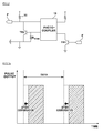
- FIG. 2 is an inverter terminal circuit diagram according to an exemplary embodiment of the present disclosure.
- a terminal circuit is configured in such a manner that an open collector output signal or a pulse output signal may be inputted through a port E, and an open collector output signal or a pulse output signal may be outputted to a port F through a photo-coupler (10).
- the port F may be connected to a device using an open collector output signal as input and to a device using a pulse output signal as input, the configuration of which may be explained by FIGS. 1a and 1b in which a port B for an open collector output terminal and a port D for a pulse output terminal are combined or integrated to allow two outputs to be outputted from the port B.
- a port E is an input port and a port F is an output port in the terminal circuit according to the present disclosure.
- a pulse output signal or an open collector output signal inputted to the port E through a transistor (TR1) may be outputted to the port F through a photo-coupler (10), a bias resistor (Rbias), a transistor (TR2).
- the bias resistor (Rbias) may be connected to a base (B) and an emitter terminal (E) of the transistor (TR2).
- the photo-coupler (10) may be used to electrically insulate an input signal and an output signal.
- a first output terminal of the photo-coupler (10) may be connected to a port F, and a second output may be connected to a base terminal of the transistor (TR2).
- TR2 base terminal of the transistor
- a user can check an inverter parameter through a user input unit (e.g., HMI (Human-Machine Interface) connected to an inverter, whereby it can be checked whether a relevant terminal is used as an open collector output terminal, or as a pulse output terminal.
- HMI Human-Machine Interface
- a pull-up resistor (20) connected to a collector (C) of output port F may be determined of its use by a device using a pulse output signal as input. If the device using the pulse output signal as input receives an open collector-type pulse input, no wiring is required for pull-up resistor (20). For example, there are many pulse metering devices capable of receiving an open collector-type pulse input.
- a pull-up resistor (20) may be connected when a device not receiving an open collector-type pulse input is connected for pulse input.
- a resistance value of the pull-up resistor (20) may be determined in consideration of time constant.
- the time constant is an index indicating how fast or slow a certain circuit reacts to an input from outside, and therefore may vary depending on characteristic of a circuit.
- the resistance of the pull-up resistor (20) may be determined in consideration of a time constant of a circuit.
- the terminal circuit according to the present disclosure When a pulse is outputted through a terminal circuit of the present disclosure, selection of a time constant configured to guarantee a pulse output is required, because a circuit using an open collector output as pulse output. That is, the terminal circuit according to the present disclosure generates a rising time and a falling time of pulse output signal according to a time constant at the time of pulse output, and the rising time and the falling time have an influence on a duty of the pulse output signal.
- FIG. 3a and 3b are exemplary views illustrating an actual pulse and a pulse by compensation at the time of pulse output according to an exemplary embodiment of the present disclosure, where FIG.3a illustrates a case when a pulse is outputted at a frequency of 1kHz, and FIG. 3b illustrates a case when a pulse is outputted at a frequency of 32kHz.
- bias resistor (Rbias) of the photo-coupler (10) may be determined for selection of a time constant guaranteeing a pulse output.
- bias resistor (Rbias) of the photo-coupler (10) can be adequately designed for guaranteeing a duty ratio of pulse within a predetermined scope.
- whether to output a pulse output signal or an open collector output signal may be possible by setting of inverter parameter.
- a user may set an inverter parameter through a user input (e.g., HMI) to output an open collector output signal or only a pulse output signal.
- a user input e.g., HMI
Landscapes
- Engineering & Computer Science (AREA)
- Physics & Mathematics (AREA)
- Computer Hardware Design (AREA)
- Computer Networks & Wireless Communication (AREA)
- Signal Processing (AREA)
- Electromagnetism (AREA)
- Computing Systems (AREA)
- General Engineering & Computer Science (AREA)
- Mathematical Physics (AREA)
- Mechanical Engineering (AREA)
- Power Engineering (AREA)
- Electronic Switches (AREA)
- Inverter Devices (AREA)
- Power Conversion In General (AREA)
- Logic Circuits (AREA)
Abstract
Description
- The teachings in accordance with the exemplary embodiments of this present disclosure generally relate to a terminal circuit in an inverter.
- In general, an electric output of an inverter is outputted through various terminals and hardware realized with a terminal circuit is commonly called a terminal block.
FIGS. 1a and 1b are circuit diagrams illustrating terminals used for an inverter according to prior art, whereFIG. 1a is a circuit diagram of a terminal relative to an output of open collector andFIG. 1b is a circuit diagram of a terminal relative to a pulse output. - It can be noted that an output signal of the open collector in
FIG. 1a is inputted to a port A to be outputted to a port B through a photo coupler and a transistor, and a pulse output signal inFIG. 1b is inputted to a port C to be outputted to a port D through a transistor. As noted above, an open collector output and a pulse output in an inverter are respectively independent in function thereof, where each terminal is formed separately to be outputted to a separate terminal block to disadvantageously restrict miniaturization of size of input/output unit of inverter, to increase the number of terminal blocks and to thereby increase the inverter costs. - The present disclosure is to provide a terminal circuit in an inverter configured to process both an open collector output and a pulse output through one single terminal block, thereby reducing the number of terminal blocks and the costs.
- In one general aspect of the present disclosure, there is provided a terminal circuit in an inverter, the terminal circuit comprising:
- a photo-coupler configured to electrically insulate input/output signals, to receive, as input, an open collector output signal or a pulse output signal from a first port and to output the open collector output signal or the pulse output signal to a second port through a first output terminal;
- a transistor in which a base (B) terminal is connected to a second output terminal of the photo-coupler; and
- a bias resistor connected to a base (B) terminal of the transistor and to an emitter (E) terminal, wherein a resistance value of the bias resistor may be so determined as to allow a duty ratio of the pulse output signal to be within a predetermined scope.
- Preferably, but not necessarily, any one of the open collector output signal and the pulse output signal may be received through the first port by an inverter parameter inputted from a user input unit.
- Preferably, but not necessarily, the terminal circuit may further comprise a pull-up resistor connected between the first output terminal of the photo-coupler and the second port.
- The exemplary embodiments of this present disclosure has an advantageous effect in that size of inverter terminals can be reduced and a duty compensation design can be provided at the time of pulse output by using a single terminal configured to perform a dual (two-way) function of an open collector output function and a pulse output function. Another advantageous effect is that an open collector output function and a pulse output function can be selectively chosen by parameter setting to allow free conversion between these two functions.
-
-
FIGS. 1a and 1b are circuit diagrams illustrating terminals used for an inverter according to prior art. -
FIG. 2 is an inverter terminal circuit diagram according to an exemplary embodiment of the present disclosure. -
FIG. 3a and3b are exemplary views illustrating an actual pulse and a pulse by compensation at the time of pulse output according to an exemplary embodiment of the present disclosure. - Various exemplary embodiments will be described more fully hereinafter with reference to the accompanying drawings, in which some exemplary embodiments are shown. The present inventive concept may, however, be embodied in many different forms and should not be construed as limited to the example embodiments set forth herein. Rather, the described aspect is intended to embrace all such alterations, modifications, and variations that fall within the scope and novel idea of the present disclosure.
- Hereinafter, exemplary embodiments of the present disclosure will be described in detail with reference to the accompanying drawings.
-
FIG. 2 is an inverter terminal circuit diagram according to an exemplary embodiment of the present disclosure. - Referring to
FIG. 2 , a terminal circuit according to the present disclosure is configured in such a manner that an open collector output signal or a pulse output signal may be inputted through a port E, and an open collector output signal or a pulse output signal may be outputted to a port F through a photo-coupler (10). - Thus, the port F may be connected to a device using an open collector output signal as input and to a device using a pulse output signal as input, the configuration of which may be explained by
FIGS. 1a and 1b in which a port B for an open collector output terminal and a port D for a pulse output terminal are combined or integrated to allow two outputs to be outputted from the port B. - That is, a port E is an input port and a port F is an output port in the terminal circuit according to the present disclosure. Thus, a pulse output signal or an open collector output signal inputted to the port E through a transistor (TR1) may be outputted to the port F through a photo-coupler (10), a bias resistor (Rbias), a transistor (TR2). The bias resistor (Rbias) may be connected to a base (B) and an emitter terminal (E) of the transistor (TR2).
- The photo-coupler (10) may be used to electrically insulate an input signal and an output signal. A first output terminal of the photo-coupler (10) may be connected to a port F, and a second output may be connected to a base terminal of the transistor (TR2). A user can check an inverter parameter through a user input unit (e.g., HMI (Human-Machine Interface) connected to an inverter, whereby it can be checked whether a relevant terminal is used as an open collector output terminal, or as a pulse output terminal.
- A pull-up resistor (20) connected to a collector (C) of output port F (or transistor TR2) may be determined of its use by a device using a pulse output signal as input. If the device using the pulse output signal as input receives an open collector-type pulse input, no wiring is required for pull-up resistor (20). For example, there are many pulse metering devices capable of receiving an open collector-type pulse input. A pull-up resistor (20) may be connected when a device not receiving an open collector-type pulse input is connected for pulse input.
- A resistance value of the pull-up resistor (20) may be determined in consideration of time constant. The time constant is an index indicating how fast or slow a certain circuit reacts to an input from outside, and therefore may vary depending on characteristic of a circuit. Thus, the resistance of the pull-up resistor (20) may be determined in consideration of a time constant of a circuit.
- When a pulse is outputted through a terminal circuit of the present disclosure, selection of a time constant configured to guarantee a pulse output is required, because a circuit using an open collector output as pulse output. That is, the terminal circuit according to the present disclosure generates a rising time and a falling time of pulse output signal according to a time constant at the time of pulse output, and the rising time and the falling time have an influence on a duty of the pulse output signal.
-
FIG. 3a and3b are exemplary views illustrating an actual pulse and a pulse by compensation at the time of pulse output according to an exemplary embodiment of the present disclosure, whereFIG.3a illustrates a case when a pulse is outputted at a frequency of 1kHz, andFIG. 3b illustrates a case when a pulse is outputted at a frequency of 32kHz. - Referring first to
FIG. 3a , when a pulse is outputted at a frequency of 1kHz with 50% duty ratio, it can be noted that the duty ratio decreases below 50% in response to a rising time and a falling time. In the present disclosure, a value of bias resistor (Rbias) of the photo-coupler (10) may be determined for selection of a time constant guaranteeing a pulse output. - Now, referring to
FIG.3b , when a pulse is outputted at a frequency of 32kHz with 50% duty ratio, it can be noted that the duty ratio of pulse further decreases over that ofFIG. 3a due to fast frequency. In the present disclosure, a value of bias resistor (Rbias) of the photo-coupler (10) can be adequately designed for guaranteeing a duty ratio of pulse within a predetermined scope. - In the present disclosure, whether to output a pulse output signal or an open collector output signal may be possible by setting of inverter parameter. A user may set an inverter parameter through a user input (e.g., HMI) to output an open collector output signal or only a pulse output signal.
- Although the present disclosure has been described in detail with reference to the foregoing embodiments and advantages, many alternatives, modifications, and variations will be apparent to those skilled in the art within the metes and bounds of the claims. Therefore, it should be understood that the above-described embodiments are not limited by any of the details of the foregoing description, unless otherwise specified, but rather should be construed broadly within the scope as defined in the appended claims
Claims (3)
- A terminal circuit in an inverter, the terminal circuit characterized by:a photo-coupler (10) configured to electrically insulate input/output signals, to receive, as input, an open collector output signal or a pulse output signal from a first port (E) and to output the open collector output signal or the pulse output signal to a second port (F) through a first output terminal;a transistor (TR2) in which a base (B) terminal is connected to a second output terminal of the photo-coupler; anda bias resistor connected to a base (B) terminal of the transistor and to an emitter (E) terminal,wherein a resistance value of the bias resistor is so determined as to allow a duty ratio of the pulse output signal to be within a predetermined scope.
- The terminal circuit of claim 1, characterized in that any one of the open collector output signal and the pulse output signal is received through the first port by an inverter parameter inputted from a user input unit.
- The terminal circuit of claim 1, further characterized by a pull-up resistor (20) connected between the first output terminal of the photo-coupler (10) and the second port (F).
Applications Claiming Priority (1)
| Application Number | Priority Date | Filing Date | Title |
|---|---|---|---|
| KR1020140006669A KR101622017B1 (en) | 2014-01-20 | 2014-01-20 | Terminal circuit in inverter |
Publications (2)
| Publication Number | Publication Date |
|---|---|
| EP2897292A1 true EP2897292A1 (en) | 2015-07-22 |
| EP2897292B1 EP2897292B1 (en) | 2018-11-21 |
Family
ID=52347192
Family Applications (1)
| Application Number | Title | Priority Date | Filing Date |
|---|---|---|---|
| EP15151211.8A Active EP2897292B1 (en) | 2014-01-20 | 2015-01-15 | Terminal circuit in inverter |
Country Status (6)
| Country | Link |
|---|---|
| US (1) | US9407167B2 (en) |
| EP (1) | EP2897292B1 (en) |
| JP (1) | JP6046754B2 (en) |
| KR (1) | KR101622017B1 (en) |
| CN (1) | CN104796133B (en) |
| ES (1) | ES2703377T3 (en) |
Families Citing this family (1)
| Publication number | Priority date | Publication date | Assignee | Title |
|---|---|---|---|---|
| CN108039882A (en) * | 2017-12-08 | 2018-05-15 | 中车大连电力牵引研发中心有限公司 | Collector two directions' inputing output circuit |
Citations (3)
| Publication number | Priority date | Publication date | Assignee | Title |
|---|---|---|---|---|
| US4321487A (en) * | 1980-04-07 | 1982-03-23 | Reliance Electric Company | Common mode rejection coupler |
| US20050069326A1 (en) * | 2003-09-30 | 2005-03-31 | Stmicroelectronics S.A. | Optical coupling device and method for bidirectional data communication over a common signal line |
| WO2012117472A1 (en) * | 2011-03-03 | 2012-09-07 | 株式会社パトライト | Input circuit and integrated circuit having the input circuit integrated therein |
Family Cites Families (10)
| Publication number | Priority date | Publication date | Assignee | Title |
|---|---|---|---|---|
| JPS58166146U (en) * | 1982-03-29 | 1983-11-05 | 横河電機株式会社 | Pulse transmission circuit using photocoupler |
| US4596048A (en) * | 1983-04-04 | 1986-06-17 | General Electric Company | Optically isolated contention bus |
| JPH1031263A (en) * | 1996-07-12 | 1998-02-03 | Canon Inc | camera |
| JPH11313030A (en) * | 1998-04-30 | 1999-11-09 | Seiko Epson Corp | Remote control signal switching circuit and signal switching circuit |
| JP2011108036A (en) * | 2009-11-18 | 2011-06-02 | Panasonic Electric Works Co Ltd | Digital input circuit |
| JP4944939B2 (en) | 2009-11-25 | 2012-06-06 | パナソニック電工Sunx株式会社 | Digital output circuit |
| CN103001512A (en) * | 2011-09-15 | 2013-03-27 | 无锡市幅瑞自动化科技有限公司 | Control system based on inverter power source |
| JP2013112905A (en) * | 2011-11-28 | 2013-06-10 | Toray Ind Inc | Sheet-like material |
| CN202772809U (en) * | 2012-09-12 | 2013-03-06 | 南京师范大学 | Low-power miniature vehicle-mounted inverter |
| JP5794352B2 (en) * | 2013-05-29 | 2015-10-14 | 株式会社デンソー | Receiving device and method for detecting number of same-value bits in received bit string |
-
2014
- 2014-01-20 KR KR1020140006669A patent/KR101622017B1/en active Active
-
2015
- 2015-01-14 US US14/597,068 patent/US9407167B2/en active Active
- 2015-01-15 ES ES15151211T patent/ES2703377T3/en active Active
- 2015-01-15 EP EP15151211.8A patent/EP2897292B1/en active Active
- 2015-01-19 JP JP2015007714A patent/JP6046754B2/en not_active Expired - Fee Related
- 2015-01-19 CN CN201510089061.4A patent/CN104796133B/en active Active
Patent Citations (3)
| Publication number | Priority date | Publication date | Assignee | Title |
|---|---|---|---|---|
| US4321487A (en) * | 1980-04-07 | 1982-03-23 | Reliance Electric Company | Common mode rejection coupler |
| US20050069326A1 (en) * | 2003-09-30 | 2005-03-31 | Stmicroelectronics S.A. | Optical coupling device and method for bidirectional data communication over a common signal line |
| WO2012117472A1 (en) * | 2011-03-03 | 2012-09-07 | 株式会社パトライト | Input circuit and integrated circuit having the input circuit integrated therein |
Also Published As
| Publication number | Publication date |
|---|---|
| ES2703377T3 (en) | 2019-03-08 |
| JP6046754B2 (en) | 2016-12-21 |
| KR20150086690A (en) | 2015-07-29 |
| EP2897292B1 (en) | 2018-11-21 |
| CN104796133B (en) | 2018-06-05 |
| KR101622017B1 (en) | 2016-05-17 |
| CN104796133A (en) | 2015-07-22 |
| US20150207430A1 (en) | 2015-07-23 |
| JP2015139222A (en) | 2015-07-30 |
| US9407167B2 (en) | 2016-08-02 |
Similar Documents
| Publication | Publication Date | Title |
|---|---|---|
| US9225196B2 (en) | Rectifying-and-modulating circuit and wireless power receiver incorporating the same | |
| US20150130439A1 (en) | Current balancing device and method | |
| US20150349777A1 (en) | Switching circuit and electronic device | |
| WO2021096307A3 (en) | Electronic device for performing communication connection to external electronic device and operation method thereof | |
| CN103780098A (en) | Output voltage feedback circuit, isolated converter and integrated circuit used therein | |
| CN104536314A (en) | NFC-based startup control circuit, method and electronic device | |
| US9407167B2 (en) | Terminal circuit in inverter | |
| US20110114858A1 (en) | Digital input circuit | |
| US20140323042A1 (en) | Watch with wireless communication functionality | |
| US9075590B2 (en) | Voltage identification definition reference voltage generation circuit and boot voltage generating method thereof | |
| CN108923780A (en) | Signal isolation circuit and optical coupler communication circuit with same | |
| WO2017124762A1 (en) | Switch control device and method for electronic device, and electronic device | |
| US8897429B2 (en) | Communication circuit employing optocoupler | |
| KR20140092547A (en) | USB OTG auto change device | |
| US9425613B2 (en) | Current limiting circuit | |
| CN204761415U (en) | Light separates terminal with output protect function | |
| CN106773903A (en) | A kind of signal circuit and terminal board | |
| CN103378910A (en) | Electronic equipment capable of preventing signal crosstalk | |
| CN205541928U (en) | Buzzer | |
| CN204203435U (en) | A kind of mobile terminal with electrical measurement function | |
| CN220543424U (en) | Electronic doorbell and control circuit thereof | |
| US12537458B2 (en) | Synchronous rectifier device for power converter | |
| GB2389429A (en) | Electronic accessory detection and identification | |
| CN106468897B (en) | Interface device and processing system | |
| JP2012191464A (en) | Level conversion bus switch |
Legal Events
| Date | Code | Title | Description |
|---|---|---|---|
| PUAI | Public reference made under article 153(3) epc to a published international application that has entered the european phase |
Free format text: ORIGINAL CODE: 0009012 |
|
| 17P | Request for examination filed |
Effective date: 20150115 |
|
| AK | Designated contracting states |
Kind code of ref document: A1 Designated state(s): AL AT BE BG CH CY CZ DE DK EE ES FI FR GB GR HR HU IE IS IT LI LT LU LV MC MK MT NL NO PL PT RO RS SE SI SK SM TR |
|
| AX | Request for extension of the european patent |
Extension state: BA ME |
|
| 17P | Request for examination filed |
Effective date: 20160126 |
|
| RBV | Designated contracting states (corrected) |
Designated state(s): AL AT BE BG CH CY CZ DE DK EE ES FI FR GB GR HR HU IE IS IT LI LT LU LV MC MK MT NL NO PL PT RO RS SE SI SK SM TR |
|
| STAA | Information on the status of an ep patent application or granted ep patent |
Free format text: STATUS: EXAMINATION IS IN PROGRESS |
|
| 17Q | First examination report despatched |
Effective date: 20170321 |
|
| GRAP | Despatch of communication of intention to grant a patent |
Free format text: ORIGINAL CODE: EPIDOSNIGR1 |
|
| STAA | Information on the status of an ep patent application or granted ep patent |
Free format text: STATUS: GRANT OF PATENT IS INTENDED |
|
| INTG | Intention to grant announced |
Effective date: 20180723 |
|
| GRAS | Grant fee paid |
Free format text: ORIGINAL CODE: EPIDOSNIGR3 |
|
| GRAA | (expected) grant |
Free format text: ORIGINAL CODE: 0009210 |
|
| STAA | Information on the status of an ep patent application or granted ep patent |
Free format text: STATUS: THE PATENT HAS BEEN GRANTED |
|
| AK | Designated contracting states |
Kind code of ref document: B1 Designated state(s): AL AT BE BG CH CY CZ DE DK EE ES FI FR GB GR HR HU IE IS IT LI LT LU LV MC MK MT NL NO PL PT RO RS SE SI SK SM TR |
|
| REG | Reference to a national code |
Ref country code: CH Ref legal event code: EP |
|
| REG | Reference to a national code |
Ref country code: IE Ref legal event code: FG4D |
|
| REG | Reference to a national code |
Ref country code: DE Ref legal event code: R096 Ref document number: 602015019942 Country of ref document: DE |
|
| REG | Reference to a national code |
Ref country code: AT Ref legal event code: REF Ref document number: 1068743 Country of ref document: AT Kind code of ref document: T Effective date: 20181215 |
|
| REG | Reference to a national code |
Ref country code: ES Ref legal event code: FG2A Ref document number: 2703377 Country of ref document: ES Kind code of ref document: T3 Effective date: 20190308 |
|
| REG | Reference to a national code |
Ref country code: NL Ref legal event code: MP Effective date: 20181121 |
|
| REG | Reference to a national code |
Ref country code: AT Ref legal event code: MK05 Ref document number: 1068743 Country of ref document: AT Kind code of ref document: T Effective date: 20181121 |
|
| PG25 | Lapsed in a contracting state [announced via postgrant information from national office to epo] |
Ref country code: IS Free format text: LAPSE BECAUSE OF FAILURE TO SUBMIT A TRANSLATION OF THE DESCRIPTION OR TO PAY THE FEE WITHIN THE PRESCRIBED TIME-LIMIT Effective date: 20190321 Ref country code: NO Free format text: LAPSE BECAUSE OF FAILURE TO SUBMIT A TRANSLATION OF THE DESCRIPTION OR TO PAY THE FEE WITHIN THE PRESCRIBED TIME-LIMIT Effective date: 20190221 Ref country code: BG Free format text: LAPSE BECAUSE OF FAILURE TO SUBMIT A TRANSLATION OF THE DESCRIPTION OR TO PAY THE FEE WITHIN THE PRESCRIBED TIME-LIMIT Effective date: 20190221 Ref country code: LT Free format text: LAPSE BECAUSE OF FAILURE TO SUBMIT A TRANSLATION OF THE DESCRIPTION OR TO PAY THE FEE WITHIN THE PRESCRIBED TIME-LIMIT Effective date: 20181121 Ref country code: LV Free format text: LAPSE BECAUSE OF FAILURE TO SUBMIT A TRANSLATION OF THE DESCRIPTION OR TO PAY THE FEE WITHIN THE PRESCRIBED TIME-LIMIT Effective date: 20181121 Ref country code: AT Free format text: LAPSE BECAUSE OF FAILURE TO SUBMIT A TRANSLATION OF THE DESCRIPTION OR TO PAY THE FEE WITHIN THE PRESCRIBED TIME-LIMIT Effective date: 20181121 Ref country code: HR Free format text: LAPSE BECAUSE OF FAILURE TO SUBMIT A TRANSLATION OF THE DESCRIPTION OR TO PAY THE FEE WITHIN THE PRESCRIBED TIME-LIMIT Effective date: 20181121 Ref country code: FI Free format text: LAPSE BECAUSE OF FAILURE TO SUBMIT A TRANSLATION OF THE DESCRIPTION OR TO PAY THE FEE WITHIN THE PRESCRIBED TIME-LIMIT Effective date: 20181121 |
|
| PG25 | Lapsed in a contracting state [announced via postgrant information from national office to epo] |
Ref country code: PT Free format text: LAPSE BECAUSE OF FAILURE TO SUBMIT A TRANSLATION OF THE DESCRIPTION OR TO PAY THE FEE WITHIN THE PRESCRIBED TIME-LIMIT Effective date: 20190321 Ref country code: SE Free format text: LAPSE BECAUSE OF FAILURE TO SUBMIT A TRANSLATION OF THE DESCRIPTION OR TO PAY THE FEE WITHIN THE PRESCRIBED TIME-LIMIT Effective date: 20181121 Ref country code: AL Free format text: LAPSE BECAUSE OF FAILURE TO SUBMIT A TRANSLATION OF THE DESCRIPTION OR TO PAY THE FEE WITHIN THE PRESCRIBED TIME-LIMIT Effective date: 20181121 Ref country code: RS Free format text: LAPSE BECAUSE OF FAILURE TO SUBMIT A TRANSLATION OF THE DESCRIPTION OR TO PAY THE FEE WITHIN THE PRESCRIBED TIME-LIMIT Effective date: 20181121 Ref country code: GR Free format text: LAPSE BECAUSE OF FAILURE TO SUBMIT A TRANSLATION OF THE DESCRIPTION OR TO PAY THE FEE WITHIN THE PRESCRIBED TIME-LIMIT Effective date: 20190222 Ref country code: NL Free format text: LAPSE BECAUSE OF FAILURE TO SUBMIT A TRANSLATION OF THE DESCRIPTION OR TO PAY THE FEE WITHIN THE PRESCRIBED TIME-LIMIT Effective date: 20181121 |
|
| PG25 | Lapsed in a contracting state [announced via postgrant information from national office to epo] |
Ref country code: DK Free format text: LAPSE BECAUSE OF FAILURE TO SUBMIT A TRANSLATION OF THE DESCRIPTION OR TO PAY THE FEE WITHIN THE PRESCRIBED TIME-LIMIT Effective date: 20181121 Ref country code: PL Free format text: LAPSE BECAUSE OF FAILURE TO SUBMIT A TRANSLATION OF THE DESCRIPTION OR TO PAY THE FEE WITHIN THE PRESCRIBED TIME-LIMIT Effective date: 20181121 Ref country code: CZ Free format text: LAPSE BECAUSE OF FAILURE TO SUBMIT A TRANSLATION OF THE DESCRIPTION OR TO PAY THE FEE WITHIN THE PRESCRIBED TIME-LIMIT Effective date: 20181121 |
|
| REG | Reference to a national code |
Ref country code: DE Ref legal event code: R097 Ref document number: 602015019942 Country of ref document: DE |
|
| PG25 | Lapsed in a contracting state [announced via postgrant information from national office to epo] |
Ref country code: EE Free format text: LAPSE BECAUSE OF FAILURE TO SUBMIT A TRANSLATION OF THE DESCRIPTION OR TO PAY THE FEE WITHIN THE PRESCRIBED TIME-LIMIT Effective date: 20181121 Ref country code: MC Free format text: LAPSE BECAUSE OF FAILURE TO SUBMIT A TRANSLATION OF THE DESCRIPTION OR TO PAY THE FEE WITHIN THE PRESCRIBED TIME-LIMIT Effective date: 20181121 Ref country code: RO Free format text: LAPSE BECAUSE OF FAILURE TO SUBMIT A TRANSLATION OF THE DESCRIPTION OR TO PAY THE FEE WITHIN THE PRESCRIBED TIME-LIMIT Effective date: 20181121 Ref country code: SK Free format text: LAPSE BECAUSE OF FAILURE TO SUBMIT A TRANSLATION OF THE DESCRIPTION OR TO PAY THE FEE WITHIN THE PRESCRIBED TIME-LIMIT Effective date: 20181121 Ref country code: SM Free format text: LAPSE BECAUSE OF FAILURE TO SUBMIT A TRANSLATION OF THE DESCRIPTION OR TO PAY THE FEE WITHIN THE PRESCRIBED TIME-LIMIT Effective date: 20181121 |
|
| REG | Reference to a national code |
Ref country code: CH Ref legal event code: PL |
|
| PLBE | No opposition filed within time limit |
Free format text: ORIGINAL CODE: 0009261 |
|
| STAA | Information on the status of an ep patent application or granted ep patent |
Free format text: STATUS: NO OPPOSITION FILED WITHIN TIME LIMIT |
|
| PG25 | Lapsed in a contracting state [announced via postgrant information from national office to epo] |
Ref country code: LU Free format text: LAPSE BECAUSE OF NON-PAYMENT OF DUE FEES Effective date: 20190115 |
|
| REG | Reference to a national code |
Ref country code: BE Ref legal event code: MM Effective date: 20190131 |
|
| 26N | No opposition filed |
Effective date: 20190822 |
|
| REG | Reference to a national code |
Ref country code: IE Ref legal event code: MM4A |
|
| PG25 | Lapsed in a contracting state [announced via postgrant information from national office to epo] |
Ref country code: SI Free format text: LAPSE BECAUSE OF FAILURE TO SUBMIT A TRANSLATION OF THE DESCRIPTION OR TO PAY THE FEE WITHIN THE PRESCRIBED TIME-LIMIT Effective date: 20181121 |
|
| PG25 | Lapsed in a contracting state [announced via postgrant information from national office to epo] |
Ref country code: BE Free format text: LAPSE BECAUSE OF NON-PAYMENT OF DUE FEES Effective date: 20190131 |
|
| PG25 | Lapsed in a contracting state [announced via postgrant information from national office to epo] |
Ref country code: LI Free format text: LAPSE BECAUSE OF NON-PAYMENT OF DUE FEES Effective date: 20190131 Ref country code: CH Free format text: LAPSE BECAUSE OF NON-PAYMENT OF DUE FEES Effective date: 20190131 |
|
| PG25 | Lapsed in a contracting state [announced via postgrant information from national office to epo] |
Ref country code: IE Free format text: LAPSE BECAUSE OF NON-PAYMENT OF DUE FEES Effective date: 20190115 |
|
| PGFP | Annual fee paid to national office [announced via postgrant information from national office to epo] |
Ref country code: FR Payment date: 20191223 Year of fee payment: 6 |
|
| PG25 | Lapsed in a contracting state [announced via postgrant information from national office to epo] |
Ref country code: TR Free format text: LAPSE BECAUSE OF FAILURE TO SUBMIT A TRANSLATION OF THE DESCRIPTION OR TO PAY THE FEE WITHIN THE PRESCRIBED TIME-LIMIT Effective date: 20181121 |
|
| PG25 | Lapsed in a contracting state [announced via postgrant information from national office to epo] |
Ref country code: MT Free format text: LAPSE BECAUSE OF NON-PAYMENT OF DUE FEES Effective date: 20190115 |
|
| PG25 | Lapsed in a contracting state [announced via postgrant information from national office to epo] |
Ref country code: CY Free format text: LAPSE BECAUSE OF FAILURE TO SUBMIT A TRANSLATION OF THE DESCRIPTION OR TO PAY THE FEE WITHIN THE PRESCRIBED TIME-LIMIT Effective date: 20181121 |
|
| PG25 | Lapsed in a contracting state [announced via postgrant information from national office to epo] |
Ref country code: HU Free format text: LAPSE BECAUSE OF FAILURE TO SUBMIT A TRANSLATION OF THE DESCRIPTION OR TO PAY THE FEE WITHIN THE PRESCRIBED TIME-LIMIT; INVALID AB INITIO Effective date: 20150115 |
|
| PG25 | Lapsed in a contracting state [announced via postgrant information from national office to epo] |
Ref country code: FR Free format text: LAPSE BECAUSE OF NON-PAYMENT OF DUE FEES Effective date: 20210131 |
|
| PG25 | Lapsed in a contracting state [announced via postgrant information from national office to epo] |
Ref country code: MK Free format text: LAPSE BECAUSE OF FAILURE TO SUBMIT A TRANSLATION OF THE DESCRIPTION OR TO PAY THE FEE WITHIN THE PRESCRIBED TIME-LIMIT Effective date: 20181121 |
|
| P01 | Opt-out of the competence of the unified patent court (upc) registered |
Effective date: 20230625 |
|
| PGFP | Annual fee paid to national office [announced via postgrant information from national office to epo] |
Ref country code: GB Payment date: 20251208 Year of fee payment: 12 |
|
| PGFP | Annual fee paid to national office [announced via postgrant information from national office to epo] |
Ref country code: ES Payment date: 20260213 Year of fee payment: 12 |
|
| PGFP | Annual fee paid to national office [announced via postgrant information from national office to epo] |
Ref country code: DE Payment date: 20251208 Year of fee payment: 12 |
|
| PGFP | Annual fee paid to national office [announced via postgrant information from national office to epo] |
Ref country code: IT Payment date: 20251209 Year of fee payment: 12 |