EP2894787A1 - High-speed successive approximation analog-to-digital converter - Google Patents
High-speed successive approximation analog-to-digital converter Download PDFInfo
- Publication number
- EP2894787A1 EP2894787A1 EP15150197.0A EP15150197A EP2894787A1 EP 2894787 A1 EP2894787 A1 EP 2894787A1 EP 15150197 A EP15150197 A EP 15150197A EP 2894787 A1 EP2894787 A1 EP 2894787A1
- Authority
- EP
- European Patent Office
- Prior art keywords
- capacitors
- analog
- successive approximation
- digital
- approximation register
- Prior art date
- Legal status (The legal status is an assumption and is not a legal conclusion. Google has not performed a legal analysis and makes no representation as to the accuracy of the status listed.)
- Withdrawn
Links
- 239000003990 capacitor Substances 0.000 claims abstract description 121
- 230000003247 decreasing effect Effects 0.000 claims abstract description 5
- 230000008878 coupling Effects 0.000 claims 1
- 238000010168 coupling process Methods 0.000 claims 1
- 238000005859 coupling reaction Methods 0.000 claims 1
- 238000000034 method Methods 0.000 description 3
- 238000004364 calculation method Methods 0.000 description 2
- 238000006243 chemical reaction Methods 0.000 description 2
- 238000005516 engineering process Methods 0.000 description 2
- 238000012986 modification Methods 0.000 description 2
- 230000004048 modification Effects 0.000 description 2
- 230000001419 dependent effect Effects 0.000 description 1
- 229920005994 diacetyl cellulose Polymers 0.000 description 1
- 238000004519 manufacturing process Methods 0.000 description 1
Images



Classifications
-
- H—ELECTRICITY
- H03—ELECTRONIC CIRCUITRY
- H03M—CODING; DECODING; CODE CONVERSION IN GENERAL
- H03M1/00—Analogue/digital conversion; Digital/analogue conversion
- H03M1/12—Analogue/digital converters
- H03M1/34—Analogue value compared with reference values
- H03M1/38—Analogue value compared with reference values sequentially only, e.g. successive approximation type
- H03M1/40—Analogue value compared with reference values sequentially only, e.g. successive approximation type recirculation type
- H03M1/403—Analogue value compared with reference values sequentially only, e.g. successive approximation type recirculation type using switched capacitors
-
- H—ELECTRICITY
- H03—ELECTRONIC CIRCUITRY
- H03M—CODING; DECODING; CODE CONVERSION IN GENERAL
- H03M1/00—Analogue/digital conversion; Digital/analogue conversion
- H03M1/06—Continuously compensating for, or preventing, undesired influence of physical parameters
- H03M1/0617—Continuously compensating for, or preventing, undesired influence of physical parameters characterised by the use of methods or means not specific to a particular type of detrimental influence
- H03M1/0675—Continuously compensating for, or preventing, undesired influence of physical parameters characterised by the use of methods or means not specific to a particular type of detrimental influence using redundancy
- H03M1/069—Continuously compensating for, or preventing, undesired influence of physical parameters characterised by the use of methods or means not specific to a particular type of detrimental influence using redundancy by range overlap between successive stages or steps
-
- H—ELECTRICITY
- H03—ELECTRONIC CIRCUITRY
- H03M—CODING; DECODING; CODE CONVERSION IN GENERAL
- H03M1/00—Analogue/digital conversion; Digital/analogue conversion
- H03M1/06—Continuously compensating for, or preventing, undesired influence of physical parameters
- H03M1/0617—Continuously compensating for, or preventing, undesired influence of physical parameters characterised by the use of methods or means not specific to a particular type of detrimental influence
- H03M1/0675—Continuously compensating for, or preventing, undesired influence of physical parameters characterised by the use of methods or means not specific to a particular type of detrimental influence using redundancy
- H03M1/0678—Continuously compensating for, or preventing, undesired influence of physical parameters characterised by the use of methods or means not specific to a particular type of detrimental influence using redundancy using additional components or elements, e.g. dummy components
- H03M1/068—Continuously compensating for, or preventing, undesired influence of physical parameters characterised by the use of methods or means not specific to a particular type of detrimental influence using redundancy using additional components or elements, e.g. dummy components the original and additional components or elements being complementary to each other, e.g. CMOS
- H03M1/0682—Continuously compensating for, or preventing, undesired influence of physical parameters characterised by the use of methods or means not specific to a particular type of detrimental influence using redundancy using additional components or elements, e.g. dummy components the original and additional components or elements being complementary to each other, e.g. CMOS using a differential network structure, i.e. symmetrical with respect to ground
-
- H—ELECTRICITY
- H03—ELECTRONIC CIRCUITRY
- H03M—CODING; DECODING; CODE CONVERSION IN GENERAL
- H03M1/00—Analogue/digital conversion; Digital/analogue conversion
- H03M1/12—Analogue/digital converters
- H03M1/34—Analogue value compared with reference values
- H03M1/38—Analogue value compared with reference values sequentially only, e.g. successive approximation type
- H03M1/46—Analogue value compared with reference values sequentially only, e.g. successive approximation type with digital/analogue converter for supplying reference values to converter
- H03M1/466—Analogue value compared with reference values sequentially only, e.g. successive approximation type with digital/analogue converter for supplying reference values to converter using switched capacitors
Definitions
- the present invention relates to a successive approximation register analog-to-digital converter (SAR ADC).
- a successive approximation register analog-to-digital converter is a type of analog-to-digital converter that converts a continuous analog waveform into a discrete digital representation by a search scheme.
- the charge-redistribution SAR ADC uses a plurality of capacitors.
- the capacitors are individually switched in a search scheme for the approximation of an analog input of the SAR ADC.
- the charge-redistribution technology is not a good fit for high-speed applications.
- a high-speed successive approximation register analog-to-digital converter (SAR ADC) and the manufacturing method thereof are disclosed.
- An SAR ADC in accordance with an exemplary embodiment of the invention comprises an SAR subcircuit, a digital-to-analog converter (DAC), and a comparator.
- the SAR subcircuit generates digital control bits in different cycles of a search scheme of the SAR ADC.
- the DAC comprises at least one set of capacitors.
- the DAC couples an analog input of the SAR ADC to the at least one set of capacitors and operates the at least one set of capacitors in accordance with the digital control bits.
- Each set of capacitors comprises p capacitors C p- 1 to C 0 decreasing in capacitance, where p capacitors C p -1 to C 0 are formed by 2 M capacitor cells, C p- 1 ⁇ C p -2 + C p- 3 +...+ C 0 , C p -1 includes ( 2 M -1 - 2 q ) capacitor cells, and p, q and M are numbers.
- the comparator is fed with an analog output transmitted from the DAC and generates a comparator output.
- the comparator output is coupled to the SAR subcircuit for generation of the digital control signals. Digital representation of the analog input of the SAR ADC is approximated in the search scheme.
- a analog-to-digital conversion method in accordance with an exemplary embodiment of the invention comprises the following steps: providing at least one set of capacitors in a digital-to-analog converter of a successive approximation register analog-to-digital converter, wherein each set of capacitors is formed by 2 M capacitor cells and M is a number; allocating each set of 2 M capacitor cells into p capacitors C p -1 to C 0 decreasing in capacitance, where C p- 1 ⁇ C p -2 + C p- 3 +...+ C 0 , C p -1 includes (2 M- 1 - 2 q ) capacitor cells, and p and q are numbers; and operating the successive approximation register analog-to-digital converter to get digital representation of an analog input of the successive approximation register analog-to-digital converter.
- the 2 q capacitor cells saved from the capacitor C p -1 is divided into r groups to be allocated to r different capacitors of the capacitors C p- 2 to C 1 , where r is a number. Note that in each of the r groups, the number of capacitor cells is a power of 2.
- C p-j one of the capacitors C p- 2 to C p-M has either 2 M-j or ( 2 M-j + 2 k ) capacitor cells, where k is not greater than q, and 2 M - j ⁇ 2 k .
- C 0 may have just one capacitor cell.
- the number of capacitor cells in any of the capacitors C p-M- 1 to C 1 is a power of 2.
- Fig. 1 depicts a successive approximation register analog-to-digital converter (SAR ADC) 100 in accordance with an exemplary embodiment of the invention. An analog-to-digital conversion method with respect to the SAR ADC 100 is also discussed.
- SAR ADC successive approximation register analog-to-digital converter
- the SAR ADC 100 comprises an SAR subcircuit 102, a digital-to-analog converter (DAC) 104, a comparator 106 and a decoder 108.
- the DAC 104 is especially designed for high-speed applications and no complex capacitance allocation is required.
- the SAR subcircuit 102 generates digital control bits 110 in different cycles (e.g., controlled by the clock clk_in) of a search scheme of the SAR ADC 100.
- the DAC 104 comprises at least one set of capacitors.
- the DAC 104 couples an analog input Vi of the SAR ADC 100 to the at least one set of capacitors and operates the at least one set of capacitors in accordance with the digital control bits 110.
- each set of capacitors comprises p capacitors C p -1 to C 0 decreasing in capacitance.
- the p capacitors C p -1 to C 0 are formed by 2 M capacitor cells, where C p-1 ⁇ C p- 2 + C p- 3 +...+ C 0 , and C p -1 includes (2 M- 1 - 2 q ) capacitor cells, and p, q and M are numbers.
- the comparator 106 is fed with an analog output Vdac_o transmitted from the DAC 104.
- the comparator 106 generates a comparator output 112 to be coupled to the SAR subcircuit 102 for generation of the digital control signals 110.
- the SAR subcircuit 102 further generates p digital bits B p-1 to B 0 (from MSB to LSB) in accordance with the comparator output 112.
- the decoder 108 decodes the p digital bits B p-1 to B 0 generated from the SAR subcircuit 102 into a digital representation D M to Do having ( M +1) bits.
- Digital representation D M ⁇ D 0 of the analog input Vi of the SAR ADC 100 is approximated in the search scheme (dependent on the comparator output 112.)
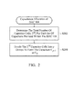
- FIG. 2 is a flowchart depicting the capacitance allocation for the DAC 104 in accordance with an exemplary embodiment of the invention.
- step S202 the total number of capacitor cells, 2 M , for each set of capacitors provided within the DAC 104 is determined.
- the set of 2 M capacitor cells may be fabricated in an array.
- step S204 the 2 M capacitor cells are divided into p groups to form the capacitors C p -1 to C 0 .
- the 2 q capacitor cells saved from the capacitor C p -1 may be divided into r groups to be allocated to r different capacitors of the capacitors C p- 2 to C 1 , where r is a number and, in each of the r groups, the number of capacitor cells is a power of 2.
- C p-j one of the capacitors C p- 2 to C p-M has either 2 M - j or (2 M-j + 2 k ) capacitor cells, where k is not greater than q and 2 M-j ⁇ 2 k .
- C 0 may have just one capacitor cell.
- the number of capacitor cells in any of the capacitors C p-M- 1 to C 1 is a power of 2.
- Figs. 3A and 4A show SAR ADCs 300 and 400 in accordance with exemplary embodiments of the invention.
- the DACs 104' and 104" are in a differential architecture, using differential input terminals Vip and Vin to receive the positive and negative differential voltages of the analog input Vi, and comprising a first set of capacitors whose top plates are connected to a positive input terminal '+' of the comparator 106 and a second set of capacitors whose top plates are connected to a negative input terminal '-' of the comparator 106.
- the comparator 106 receives an analog output Vdac_o in a differential form.
- the SAR subcircuit 102 provides the first set of capacitors in the non-inverting path with digital control bits 110_1.
- the SAR subcircuit 102 provides the second set of capacitors in the inverting path with digital control bits 110_2. During a sample phase prior to the search scheme, the analog input Vi is sampled between the top plates of the first set of capacitors (in the non-inverting path) and the top plates of the second set of capacitors (in the inverting path).
- p is 11.
- p is 12.
- the capacitors C p- 1 to C 0 of the first and second sets of capacitors correspond to p different cycles of the search scheme.
- a first set of switches are provided with the first set of capacitors (in the non-inverting path) and operated in accordance with the digital control bits 110_1.
- a second set of switches are provided with the second set of capacitors (in the inverting path) and operated in accordance with the digital control bits 110_2. Note that the capacitors (Co in both paths) corresponding to the last cycle of the p different cycles of the search scheme is not switch-controlled.
- the capacitor C 0 of the first set of capacitors (in the non-inverting path) is coupled between the positive input terminal '+' of the comparator 106 and a ground terminal.
- the capacitor C 0 of the second set of capacitors (in the inverting path) is coupled between the negative input terminal '-' of the comparator 106 and the ground terminal. Except for the last cycle, when the comparator output 112 is high, the switch for the capacitor corresponding to the current cycle in the first set of capacitors (in the non-inverting path) is switched to pull down the voltage level at the top plates of the first set of capacitors.
- the switch for the capacitor corresponding to the current cycle in the second set of capacitors is switched to pull down the voltage level at the top plates of the second set of capacitors.
- the SAR subcircuit 102 Based on the comparator output 112 during the p different cycles of the search scheme, the SAR subcircuit 102 generates the digital bits B p-1 to B 0 to be decoded by the decoder 108 for the digital representation D 9 ⁇ D 0 .
- C 10 ⁇ C 0 240, 128, 64, 36, 20, 10, 6, 4, 2, 1, 1 capacitor cell(s).
- the size of the capacitors C 10 ⁇ C 0 may be estimated by the following calculation: C 10 C 9 C 8 C 7 C 6 C 5 C 4 C 3 C 2 C 1 C 0 2 8 2 7 2 6 2 5 2 4 2 3 2 2 2 1 2 0 1 - + + + + + + + + + 2 4 ⁇ 2 2 2 2 2 1 2 1 2 1 2 0 2 0 240 128 64 36 20 10 6 4 2 1 1 1
- the approximation error that occurred in the first cycle (corresponding to C 10 ) of the search scheme can be compensated for in later cycles.
- the operation speed of the SAR ADC is no longer limited by the settling time of large-sized capacitors.
- the capacitance allocation based on a binary concept (a power of 2) is not a complex design.
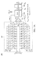
- Fig. 3B depicts the decoder 108 of the SAR ADC 300 of Fig. 3A . Only 8 full adders and 10 D-flip-flops are required. Much simpler than those for the conventional charge-redistribution design.
- C 11 ⁇ C 0 240, 128, 64, 36, 20, 10, 6, 3, 2, 1, 1, 1 capacitor cell(s).
- the size of the capacitors C 11 ⁇ C 0 may be estimated by the following calculation: C 11 C 10 C 9 C 8 C 7 C 6 C 5 C 4 C 3 C 2 C 1 C 0 2 8 2 7 2 6 2 5 2 4 2 3 2 2 2 1 2 0 1 - + + + + + + + + + + + + 2 4 ⁇ 2 2 2 2 1 2 1 2 0 2 0 2 0 2 0 240 128 64 36 20 10 6 3 2 1 1 1 1 1 1
- the 2 4 capacitor cells saved from capacitor C 11 are divided into 8 groups (more than the 7 groups designed for the SAR ADC 300 of Fig. 3A ). In this example, down to the small capacitors C 3 ⁇ C 0 the error compensation capability is still considerable.
- Fig. 4B depicts the decoder 108 of the SAR ADC 400 of Fig. 4A . Only 10 full adders and 10 D-flip-flops are required. Much simpler than those for the conventional charge-redistribution design.
Landscapes
- Engineering & Computer Science (AREA)
- Theoretical Computer Science (AREA)
- Analogue/Digital Conversion (AREA)
Abstract
Description
- The present invention relates to a successive approximation register analog-to-digital converter (SAR ADC).
- A successive approximation register analog-to-digital converter (SAR ADC) is a type of analog-to-digital converter that converts a continuous analog waveform into a discrete digital representation by a search scheme.
- One of the most common implementations of SAR ADC, the charge-redistribution SAR ADC, uses a plurality of capacitors. The capacitors are individually switched in a search scheme for the approximation of an analog input of the SAR ADC. However, because of the long settling time required for the capacitors, the charge-redistribution technology is not a good fit for high-speed applications.
- A high-speed successive approximation register analog-to-digital converter (SAR ADC) and the manufacturing method thereof are disclosed.
- An SAR ADC in accordance with an exemplary embodiment of the invention comprises an SAR subcircuit, a digital-to-analog converter (DAC), and a comparator. The SAR subcircuit generates digital control bits in different cycles of a search scheme of the SAR ADC. The DAC comprises at least one set of capacitors. The DAC couples an analog input of the SAR ADC to the at least one set of capacitors and operates the at least one set of capacitors in accordance with the digital control bits. Each set of capacitors comprises p capacitors C p-1 to C0 decreasing in capacitance, where p capacitors C p-1 to C0 are formed by 2 M capacitor cells, C p-1< C p-2 + C p-3 +...+ C0, C p-1 includes (2 M-1 - 2 q ) capacitor cells, and p, q and M are numbers. The comparator is fed with an analog output transmitted from the DAC and generates a comparator output. The comparator output is coupled to the SAR subcircuit for generation of the digital control signals. Digital representation of the analog input of the SAR ADC is approximated in the search scheme.
- A analog-to-digital conversion method in accordance with an exemplary embodiment of the invention comprises the following steps: providing at least one set of capacitors in a digital-to-analog converter of a successive approximation register analog-to-digital converter, wherein each set of capacitors is formed by 2 M capacitor cells and M is a number; allocating each set of 2M capacitor cells into p capacitors C p-1 to C0 decreasing in capacitance, where C p-1< C p-2 + C p-3 +...+ C0, C p-1 includes (2 M-1 - 2 q ) capacitor cells, and p and q are numbers; and operating the successive approximation register analog-to-digital converter to get digital representation of an analog input of the successive approximation register analog-to-digital converter.
- In some exemplary embodiments, the 2 q capacitor cells saved from the capacitor C p-1 is divided into r groups to be allocated to r different capacitors of the capacitors C p-2 to C1, where r is a number. Note that in each of the r groups, the number of capacitor cells is a power of 2.
- In some exemplary embodiments, C p-j , one of the capacitors C p-2 to Cp-M has either 2 M-j or (2 M-j + 2 k ) capacitor cells, where k is not greater than q, and 2 M-j ≠ 2 k. C0 may have just one capacitor cell. In an exemplary embodiment, the number of capacitor cells in any of the capacitors C p-M-1 to C1 is a power of 2.
- A detailed description is given in the following embodiments with reference to the accompanying drawings.
- The present invention can be more fully understood by reading the subsequent detailed description and examples with references made to the accompanying drawings, wherein:
-
Fig. 1 depicts a successive approximation register analog-to-digital converter (SAR ADC) 100 in accordance with an exemplary embodiment of the invention; -
FIG. 2 is a flowchart depicting the capacitance allocation for theDAC 104 in accordance with an exemplary embodiment of the invention; -
Fig. 3A depicts an SAR ADC in accordance with an exemplary embodiment of the invention; -
Fig. 3B depicts the decoder (DEC) 108 of the SAR ADC ofFig. 3A ; -
Fig. 4A depicts an SAR ADC in accordance with an exemplary embodiment of the invention; and -
Fig. 4B depicts the decoder (DEC) 108 of the SAR ADC ofFig. 4A . - The following description is of the best-contemplated mode of carrying out the invention. This description is made for the purpose of illustrating the general principles of the invention and should not be taken in a limiting sense. The scope of the invention is best determined by reference to the appended claims.
-
Fig. 1 depicts a successive approximation register analog-to-digital converter (SAR ADC) 100 in accordance with an exemplary embodiment of the invention. An analog-to-digital conversion method with respect to theSAR ADC 100 is also discussed. - The SAR
ADC 100 comprises anSAR subcircuit 102, a digital-to-analog converter (DAC) 104, acomparator 106 and adecoder 108. In comparison with the conventional charge-redistribution technique, theDAC 104 is especially designed for high-speed applications and no complex capacitance allocation is required. - The
SAR subcircuit 102 generatesdigital control bits 110 in different cycles (e.g., controlled by the clock clk_in) of a search scheme of the SARADC 100. TheDAC 104 comprises at least one set of capacitors. TheDAC 104 couples an analog input Vi of the SARADC 100 to the at least one set of capacitors and operates the at least one set of capacitors in accordance with thedigital control bits 110. Note that each set of capacitors comprises p capacitors C p-1 to C0 decreasing in capacitance. The p capacitors C p-1 to C0 are formed by 2 M capacitor cells, where C p-1 < C p-2 + C p-3 +...+ C0, and C p-1 includes (2 M-1 - 2 q ) capacitor cells, and p, q and M are numbers. - The
comparator 106 is fed with an analog output Vdac_o transmitted from theDAC 104. Thecomparator 106 generates acomparator output 112 to be coupled to theSAR subcircuit 102 for generation of thedigital control signals 110. TheSAR subcircuit 102 further generates p digital bits Bp-1 to B0 (from MSB to LSB) in accordance with thecomparator output 112. Thedecoder 108 decodes the p digital bits Bp-1 to B0 generated from theSAR subcircuit 102 into a digital representation DM to Do having (M+1) bits. Digital representation DM···D0 of the analog input Vi of the SAR ADC 100 is approximated in the search scheme (dependent on thecomparator output 112.) -
FIG. 2 is a flowchart depicting the capacitance allocation for theDAC 104 in accordance with an exemplary embodiment of the invention. In step S202, the total number of capacitor cells, 2 M , for each set of capacitors provided within theDAC 104 is determined. The set of 2 M capacitor cells may be fabricated in an array. In step S204, the 2 M capacitor cells are divided into p groups to form the capacitors C p-1 to C0. In addition to making C p-1< C p-2 + C p-3 +...+ C0 and C p-1 including (2 M-1 - 2 q ) capacitor cells, the 2 q capacitor cells saved from the capacitor C p-1 may be divided into r groups to be allocated to r different capacitors of the capacitors C p-2 to C1, where r is a number and, in each of the r groups, the number of capacitor cells is a power of 2. In another exemplary embodiment, C p-j , one of the capacitors C p-2 to Cp-M has either 2 M-j or (2 M-j + 2 k ) capacitor cells, where k is not greater than q and 2 M-j ≠ 2 k. C0 may have just one capacitor cell. In an exemplary embodiment, the number of capacitor cells in any of the capacitors C p-M-1 to C1 is a power of 2. -
Figs. 3A and4A showSAR ADCs DACs 104' and 104" are in a differential architecture, using differential input terminals Vip and Vin to receive the positive and negative differential voltages of the analog input Vi, and comprising a first set of capacitors whose top plates are connected to a positive input terminal '+' of thecomparator 106 and a second set of capacitors whose top plates are connected to a negative input terminal '-' of thecomparator 106. Thecomparator 106 receives an analog output Vdac_o in a differential form. The SAR subcircuit 102 provides the first set of capacitors in the non-inverting path with digital control bits 110_1. The SAR subcircuit 102 provides the second set of capacitors in the inverting path with digital control bits 110_2. During a sample phase prior to the search scheme, the analog input Vi is sampled between the top plates of the first set of capacitors (in the non-inverting path) and the top plates of the second set of capacitors (in the inverting path). - In
fig. 3A , p is 11. Infig. 4A , p is 12. The capacitors C p-1 to C0 of the first and second sets of capacitors correspond to p different cycles of the search scheme. A first set of switches are provided with the first set of capacitors (in the non-inverting path) and operated in accordance with the digital control bits 110_1. A second set of switches are provided with the second set of capacitors (in the inverting path) and operated in accordance with the digital control bits 110_2. Note that the capacitors (Co in both paths) corresponding to the last cycle of the p different cycles of the search scheme is not switch-controlled. The capacitor C0 of the first set of capacitors (in the non-inverting path) is coupled between the positive input terminal '+' of thecomparator 106 and a ground terminal. The capacitor C0 of the second set of capacitors (in the inverting path) is coupled between the negative input terminal '-' of thecomparator 106 and the ground terminal. Except for the last cycle, when thecomparator output 112 is high, the switch for the capacitor corresponding to the current cycle in the first set of capacitors (in the non-inverting path) is switched to pull down the voltage level at the top plates of the first set of capacitors. Except for the last cycle, when thecomparator output 112 is low, the switch for the capacitor corresponding to the current cycle in the second set of capacitors (in the inverting path) is switched to pull down the voltage level at the top plates of the second set of capacitors. Based on thecomparator output 112 during the p different cycles of the search scheme, theSAR subcircuit 102 generates the digital bits Bp-1 to B0 to be decoded by thedecoder 108 for the digital representation D9···D0. - In
Fig. 3A , p=11, C10∼C0 = 240, 128, 64, 36, 20, 10, 6, 4, 2, 1, 1 capacitor cell(s). The size of the capacitors C10∼C0 may be estimated by the following calculation:C10 C9 C8 C7 C6 C5 C4 C3 C2 C1 C0 28 27 26 25 24 23 22 21 20 1 - + + + + + + 24 → 22 22 21 21 21 20 20 240 128 64 36 20 10 6 4 2 1 1 - Because C10 < C9 + C8 +...+ Co, the approximation error that occurred in the first cycle (corresponding to C10) of the search scheme can be compensated for in later cycles. Thus, the operation speed of the SAR ADC is no longer limited by the settling time of large-sized capacitors. Furthermore, the capacitance allocation based on a binary concept (a power of 2) is not a complex design.
-
Fig. 3B depicts thedecoder 108 of theSAR ADC 300 ofFig. 3A . Only 8 full adders and 10 D-flip-flops are required. Much simpler than those for the conventional charge-redistribution design. - In
Fig. 4A , p=12, C11∼C0 = 240, 128, 64, 36, 20, 10, 6, 3, 2, 1, 1, 1 capacitor cell(s). The size of the capacitors C11∼C0 may be estimated by the following calculation:C11 C10 C9 C8 C7 C6 C5 C4 C3 C2 C1 C0 28 27 26 25 24 23 22 21 20 1 - + + + + + + 24 → 22 22 21 21 20 20 20 20 240 128 64 36 20 10 6 3 2 1 1 1 - The 24 capacitor cells saved from capacitor C11 are divided into 8 groups (more than the 7 groups designed for the
SAR ADC 300 ofFig. 3A ). In this example, down to the small capacitors C3∼C0 the error compensation capability is still considerable. -
Fig. 4B depicts thedecoder 108 of theSAR ADC 400 ofFig. 4A . Only 10 full adders and 10 D-flip-flops are required. Much simpler than those for the conventional charge-redistribution design. - Note that it is not intended to limit the
DAC 104 to the differential architecture or to the top-plate input S/H. Any SAR ADC with the idea of charge redistribution may require the capacitance allocation technology of the disclosure. - While the invention has been described by way of example and in terms of the preferred embodiments, it is to be understood that the invention is not limited to the disclosed embodiments. On the contrary, it is intended to cover various modifications and similar arrangements (as would be apparent to those skilled in the art). Therefore, the scope of the appended claims should be accorded the broadest interpretation so as to encompass all such modifications and similar arrangements.
Claims (9)
- A successive approximation register analog-to-digital converter (100), comprising:a successive approximation register subcircuit (102), generating digital control bits (110) in different cycles of a search scheme of the successive approximation register analog-to-digital converter (100);a digital-to-analog converter (104), comprising at least one set of capacitors and coupling an analog input (Vi) of the successive approximation register analog-to-digital converter (100) to the at least one set of capacitors and operating the at least one set of capacitors in accordance with the digital control bits (110), wherein each set of capacitors comprises p capacitors C p-1 to C0 decreasing in capacitance, the p capacitors C p-1 to C0 are formed by 2 M capacitor cells, C p-1< C p-2 + C p-3 +...+ C0, C p-1 includes (2 M-1 - 2 q ) capacitor cells, and p, q and M are numbers; anda comparator (106), fed with an analog output (Vdac_o) transmitted from the digital-to-analog converter (104) and generating a comparator output (112) to be coupled to the successive approximation register subcircuit (102) for generation of the digital control signals (110),wherein digital representation (DM...D0) of the analog input (Vi) of the successive approximation register analog-to-digital converter (100) is approximated in the search scheme.
- The successive approximation register analog-to-digital converter (100) as claimed in claim 1, wherein:the 2 q capacitor cells saved from the capacitor C p-1 is divided into r groups to be allocated to r different capacitors of the capacitors C p-2 to C1, where r is a number; andin each group of the r groups, the number of capacitor cells is a power of 2.
- The successive approximation register analog-to-digital converter (100) as claimed in claim 2, wherein:C p-j , one of the capacitors C p-2 to Cp-M has either 20 M-j or (2 M-j + 2 k ) capacitor cells, where k is not greater than q, and 2 M-j ≠ 2 k.
- The successive approximation register analog-to-digital converter as claimed in claim 3, wherein:capacitor C0 has just one capacitor cell; andthe number of capacitor cells in any of the capacitors C p-M-1 to C1 is a power of 2.
- The successive approximation register analog-to-digital converter (100) as claimed in claim 1, wherein:the successive approximation register subcircuit (102) further generates p digital bits (Bp-1···B0) in accordance with the comparator output (112), to be decoded to the digital representation (DM...D0) having (M+1) bits.
- The successive approximation register analog-to-digital converter (100) as claimed in claim 5, further comprising:a decoder (108), decoding the p digital bits (Bp-1···B0) generated by the successive approximation register subcircuit (102) into the digital representation (DM...D0) having (M+1) bits.
- The successive approximation register analog-to-digital converter (300/400) as claimed in claim 1, wherein:the analog input (Vi) of the successive approximation register analog-to-digital converter (300/400) is a differential signal represented by a positive differential voltage (Vip) and a negative differential voltage (Vin);during a sample phase prior to the search scheme, the positive differential voltage (Vip) is coupled to top plates of a first set of capacitors of the digital-to-analog converter (104'/104") and the negative differential voltage (Vin) is coupled to top plates of a second set of capacitors of the digital-to-analog converter (104'/104");the top plates of the first set of capacitors are connected to a positive input terminal of the comparator (106); andthe top plates of the second set of capacitors are connected to a negative input terminal of the comparator (106).
- The successive approximation register analog-to-digital converter (300/400) as claimed in claim 7, wherein:the capacitors C p-1 to C0 (C10 to C0/C11 to C0) of the first and second sets of capacitors correspond to p different cycles of the search scheme;the capacitor C0 of the first set of capacitors is coupled between the positive input terminal of the comparator (112) and a ground terminal;the capacitor C0 of the second set of capacitors is coupled between the negative input terminal of the comparator (112) and the ground terminal; andexcept for the last cycle, when the comparator output (112) is high, the capacitor corresponding to the current cycle in the first set of capacitors is switched to pull down the voltage level at the top plates of the first set of capacitors.
- The successive approximation register analog-to-digital converter (300/400) as claimed in claim 8, wherein:except for the last cycle, when the comparator output (112) is low, the capacitor corresponding to the current cycle in the second set of capacitors is switched to pull down the voltage level at the top plates of the second set of capacitors.
Applications Claiming Priority (2)
| Application Number | Priority Date | Filing Date | Title |
|---|---|---|---|
| US201461925307P | 2014-01-09 | 2014-01-09 | |
| US14/284,177 US9172389B2 (en) | 2014-01-09 | 2014-05-21 | High-speed successive approximation analog-to-digital converter |
Publications (1)
| Publication Number | Publication Date |
|---|---|
| EP2894787A1 true EP2894787A1 (en) | 2015-07-15 |
Family
ID=52232087
Family Applications (1)
| Application Number | Title | Priority Date | Filing Date |
|---|---|---|---|
| EP15150197.0A Withdrawn EP2894787A1 (en) | 2014-01-09 | 2015-01-06 | High-speed successive approximation analog-to-digital converter |
Country Status (3)
| Country | Link |
|---|---|
| US (1) | US9172389B2 (en) |
| EP (1) | EP2894787A1 (en) |
| CN (1) | CN104779957B (en) |
Families Citing this family (6)
| Publication number | Priority date | Publication date | Assignee | Title |
|---|---|---|---|---|
| CN106817128B (en) * | 2015-12-01 | 2020-07-10 | 瑞昱半导体股份有限公司 | Method for self-adaptive regulating coding mode and its digital correcting circuit |
| KR101907028B1 (en) * | 2016-07-06 | 2018-10-11 | 주식회사 유엑스팩토리 | Analog Digital Interfaced SRAM Structure |
| CN108233925A (en) * | 2016-12-21 | 2018-06-29 | 电子科技大学 | It is segmented pre-quantization bypass gradually-appoximant analog-digital converter |
| CN106899299B (en) * | 2017-01-09 | 2019-12-10 | 电子科技大学 | capacitance reconstruction method for improving SFDR and SNDR of resistance-capacitance type successive approximation analog-to-digital converter |
| US10826520B1 (en) * | 2019-08-09 | 2020-11-03 | Texas Instruments Incorporated | Successive approximation register analog-to-digital converter |
| JP2024142266A (en) * | 2023-03-29 | 2024-10-10 | ローム株式会社 | Successive Approximation A/D Converter |
Citations (5)
| Publication number | Priority date | Publication date | Assignee | Title |
|---|---|---|---|---|
| US20120154194A1 (en) * | 2010-12-16 | 2012-06-21 | National Cheng Kung University | Successive approximation analog-to-digital converter having auxiliary prediction circuit and method thereof |
| US20120274489A1 (en) * | 2011-04-28 | 2012-11-01 | Ncku Research And Development Foundation | Successive approximation register adc with a window predictive function |
| WO2013036204A1 (en) * | 2011-09-06 | 2013-03-14 | National University Of Singapore | An analog-to-digital converter for a multi-channel signal acquisition system |
| US20130093609A1 (en) * | 2011-10-12 | 2013-04-18 | Himax Technologies Limited | Successive approximation analog to digital converter with a direct switching technique for capacitor array through comparator output and method thereof |
| US8599059B1 (en) * | 2012-09-07 | 2013-12-03 | Mediatek Inc. | Successive approximation register analog-digital converter and method for operating the same |
Family Cites Families (5)
| Publication number | Priority date | Publication date | Assignee | Title |
|---|---|---|---|---|
| DE102009005770B4 (en) * | 2009-01-23 | 2012-01-26 | Texas Instruments Deutschland Gmbh | SAR ADC and methods with INL compensation |
| WO2011028674A2 (en) * | 2009-09-01 | 2011-03-10 | The Regents Of The University Of Michigan | Low-power area-efficient sar adc using dual capacitor arrays |
| DE102011110115B4 (en) * | 2011-08-15 | 2015-02-26 | Texas Instruments Deutschland Gmbh | Apparatus and method for measuring the DNL of a SAR ADC |
| JP5869965B2 (en) * | 2012-05-31 | 2016-02-24 | 富士通株式会社 | AD conversion circuit and AD conversion method |
| CN103152049A (en) * | 2013-02-26 | 2013-06-12 | 上海宏力半导体制造有限公司 | Successive approximation register type ADC (analog-digital converter) |
-
2014
- 2014-05-21 US US14/284,177 patent/US9172389B2/en active Active
-
2015
- 2015-01-06 EP EP15150197.0A patent/EP2894787A1/en not_active Withdrawn
- 2015-01-09 CN CN201510010407.7A patent/CN104779957B/en active Active
Patent Citations (5)
| Publication number | Priority date | Publication date | Assignee | Title |
|---|---|---|---|---|
| US20120154194A1 (en) * | 2010-12-16 | 2012-06-21 | National Cheng Kung University | Successive approximation analog-to-digital converter having auxiliary prediction circuit and method thereof |
| US20120274489A1 (en) * | 2011-04-28 | 2012-11-01 | Ncku Research And Development Foundation | Successive approximation register adc with a window predictive function |
| WO2013036204A1 (en) * | 2011-09-06 | 2013-03-14 | National University Of Singapore | An analog-to-digital converter for a multi-channel signal acquisition system |
| US20130093609A1 (en) * | 2011-10-12 | 2013-04-18 | Himax Technologies Limited | Successive approximation analog to digital converter with a direct switching technique for capacitor array through comparator output and method thereof |
| US8599059B1 (en) * | 2012-09-07 | 2013-12-03 | Mediatek Inc. | Successive approximation register analog-digital converter and method for operating the same |
Non-Patent Citations (3)
| Title |
|---|
| HAO-CHIAO HONG ET AL: "A 65-fJ/Conversion-Step 0.9-V 200-kS/s Rail-to-Rail 8-bit Successive Approximation ADC", IEEE JOURNAL OF SOLID-STATE CIRCUITS, IEEE SERVICE CENTER, PISCATAWAY, NJ, USA, vol. 42, no. 10, 1 October 2007 (2007-10-01), pages 2161 - 2168, XP011193062, ISSN: 0018-9200, DOI: 10.1109/JSSC.2007.905237 * |
| KOK LIM CHAN ET AL: "A 8.9-ENOB 2.5- W 150-KS/s non-binary redundant successive approximation ADC in 0.18- m CMOS for bio-implanted devices", 2010 ANNUAL INTERNATIONAL CONFERENCE OF THE IEEE ENGINEERING IN MEDICINE AND BIOLOGY SOCIETY : (EMBC 2010) ; BUENOS AIRES, ARGENTINA, 31 AUGUST - 4 SEPTEMBER 2010, IEEE, PISCATAWAY, NJ, USA, 31 August 2010 (2010-08-31), pages 650 - 653, XP032108969, ISBN: 978-1-4244-4123-5, DOI: 10.1109/IEMBS.2010.5627231 * |
| YUKI KURISU ET AL: "A Successive Approximation A/D Converter Using Generalized Non-Binary Algorithm", MULTIPLE-VALUED LOGIC (ISMVL), 2013 IEEE 43RD INTERNATIONAL SYMPOSIUM ON, IEEE, 22 May 2013 (2013-05-22), pages 152 - 157, XP032421344, ISBN: 978-1-4673-6067-8, DOI: 10.1109/ISMVL.2013.9 * |
Also Published As
| Publication number | Publication date |
|---|---|
| CN104779957B (en) | 2018-01-12 |
| US20150194980A1 (en) | 2015-07-09 |
| CN104779957A (en) | 2015-07-15 |
| US9172389B2 (en) | 2015-10-27 |
Similar Documents
| Publication | Publication Date | Title |
|---|---|---|
| US8416116B2 (en) | Successive approximation analog-to-digital converter having auxiliary prediction circuit and method thereof | |
| KR102637630B1 (en) | Redundancy scheme for flash assisted successive approximation register(sar) analog-to-digital converter(adc) | |
| CN108574487B (en) | successive approximation register analog-to-digital converter | |
| US8638248B2 (en) | Input-independent self-calibration method and apparatus for successive approximation analog-to-digital converter with charge-redistribution digital to analog converter | |
| US9847790B2 (en) | Hybrid analog-to-digital converter using digital slope analog-to-digital converter and related hybrid analog-to-digital conversion method thereof | |
| CN101345526B (en) | Analog-to-digital converter, method of controlling the same, and wireless transceiver circuit | |
| EP3090488B1 (en) | Combining a coarse adc and a sar adc | |
| US8599059B1 (en) | Successive approximation register analog-digital converter and method for operating the same | |
| US11418209B2 (en) | Signal conversion circuit utilizing switched capacitors | |
| KR102017310B1 (en) | Successive approximation register analog digital converter and operating method thereof | |
| US9172389B2 (en) | High-speed successive approximation analog-to-digital converter | |
| Cho et al. | A 9-bit 80 MS/s successive approximation register analog-to-digital converter with a capacitor reduction technique | |
| CN103178855B (en) | Be applied to the syllogic capacitor array structure of high accuracy gradually-appoximant analog-digital converter | |
| US10840932B2 (en) | Analog-to-digital converter | |
| US20130076554A1 (en) | Successive approximation analog to digital converter | |
| CN102916701A (en) | Multiplying digital-to-analog converters and pipeline analog-to-digital converter using the same | |
| CN112039528B (en) | Capacitor array logic control method in successive approximation analog-to-digital converter | |
| CN111130550A (en) | A kind of successive approximation register type analog-to-digital converter and its signal conversion method | |
| CN112187274A (en) | Circuit for improving stability of reference voltage of successive approximation type analog-to-digital converter | |
| KR101986699B1 (en) | Successive approximation register analog digital converter and operating method thereof | |
| KR20180072908A (en) | Current steering analog-digital converter | |
| KR20140015048A (en) | Analog-to-digital converter having dc/dc converter for low voltage operation | |
| CN111431535B (en) | A 2b/cycle successive approximation analog-to-digital converter and its quantization method | |
| CN109039338B (en) | Differential capacitor array and switching method thereof | |
| Długosz et al. | Low chip area, low power dissipation, programmable, current mode, 10-bits, SAR ADC implemented in the CMOS 130nm technology |
Legal Events
| Date | Code | Title | Description |
|---|---|---|---|
| PUAI | Public reference made under article 153(3) epc to a published international application that has entered the european phase |
Free format text: ORIGINAL CODE: 0009012 |
|
| 17P | Request for examination filed |
Effective date: 20150106 |
|
| AK | Designated contracting states |
Kind code of ref document: A1 Designated state(s): AL AT BE BG CH CY CZ DE DK EE ES FI FR GB GR HR HU IE IS IT LI LT LU LV MC MK MT NL NO PL PT RO RS SE SI SK SM TR |
|
| AX | Request for extension of the european patent |
Extension state: BA ME |
|
| R17P | Request for examination filed (corrected) |
Effective date: 20160105 |
|
| RBV | Designated contracting states (corrected) |
Designated state(s): AL AT BE BG CH CY CZ DE DK EE ES FI FR GB GR HR HU IE IS IT LI LT LU LV MC MK MT NL NO PL PT RO RS SE SI SK SM TR |
|
| STAA | Information on the status of an ep patent application or granted ep patent |
Free format text: STATUS: EXAMINATION IS IN PROGRESS |
|
| 17Q | First examination report despatched |
Effective date: 20180322 |
|
| STAA | Information on the status of an ep patent application or granted ep patent |
Free format text: STATUS: THE APPLICATION HAS BEEN WITHDRAWN |
|
| 18W | Application withdrawn |
Effective date: 20190125 |