EP2894676B1 - Solar cell array having two different types of cells - Google Patents
Solar cell array having two different types of cells Download PDFInfo
- Publication number
- EP2894676B1 EP2894676B1 EP15150388.5A EP15150388A EP2894676B1 EP 2894676 B1 EP2894676 B1 EP 2894676B1 EP 15150388 A EP15150388 A EP 15150388A EP 2894676 B1 EP2894676 B1 EP 2894676B1
- Authority
- EP
- European Patent Office
- Prior art keywords
- cell
- solar cell
- cells
- type
- side edges
- Prior art date
- Legal status (The legal status is an assumption and is not a legal conclusion. Google has not performed a legal analysis and makes no representation as to the accuracy of the status listed.)
- Active
Links
Images


Classifications
-
- H—ELECTRICITY
- H10—SEMICONDUCTOR DEVICES; ELECTRIC SOLID-STATE DEVICES NOT OTHERWISE PROVIDED FOR
- H10F—INORGANIC SEMICONDUCTOR DEVICES SENSITIVE TO INFRARED RADIATION, LIGHT, ELECTROMAGNETIC RADIATION OF SHORTER WAVELENGTH OR CORPUSCULAR RADIATION
- H10F19/00—Integrated devices, or assemblies of multiple devices, comprising at least one photovoltaic cell covered by group H10F10/00, e.g. photovoltaic modules
- H10F19/90—Structures for connecting between photovoltaic cells, e.g. interconnections or insulating spacers
- H10F19/902—Structures for connecting between photovoltaic cells, e.g. interconnections or insulating spacers for series or parallel connection of photovoltaic cells
- H10F19/904—Structures for connecting between photovoltaic cells, e.g. interconnections or insulating spacers for series or parallel connection of photovoltaic cells characterised by the shapes of the structures
-
- H—ELECTRICITY
- H10—SEMICONDUCTOR DEVICES; ELECTRIC SOLID-STATE DEVICES NOT OTHERWISE PROVIDED FOR
- H10F—INORGANIC SEMICONDUCTOR DEVICES SENSITIVE TO INFRARED RADIATION, LIGHT, ELECTROMAGNETIC RADIATION OF SHORTER WAVELENGTH OR CORPUSCULAR RADIATION
- H10F19/00—Integrated devices, or assemblies of multiple devices, comprising at least one photovoltaic cell covered by group H10F10/00, e.g. photovoltaic modules
-
- H—ELECTRICITY
- H10—SEMICONDUCTOR DEVICES; ELECTRIC SOLID-STATE DEVICES NOT OTHERWISE PROVIDED FOR
- H10F—INORGANIC SEMICONDUCTOR DEVICES SENSITIVE TO INFRARED RADIATION, LIGHT, ELECTROMAGNETIC RADIATION OF SHORTER WAVELENGTH OR CORPUSCULAR RADIATION
- H10F19/00—Integrated devices, or assemblies of multiple devices, comprising at least one photovoltaic cell covered by group H10F10/00, e.g. photovoltaic modules
- H10F19/90—Structures for connecting between photovoltaic cells, e.g. interconnections or insulating spacers
- H10F19/902—Structures for connecting between photovoltaic cells, e.g. interconnections or insulating spacers for series or parallel connection of photovoltaic cells
-
- Y—GENERAL TAGGING OF NEW TECHNOLOGICAL DEVELOPMENTS; GENERAL TAGGING OF CROSS-SECTIONAL TECHNOLOGIES SPANNING OVER SEVERAL SECTIONS OF THE IPC; TECHNICAL SUBJECTS COVERED BY FORMER USPC CROSS-REFERENCE ART COLLECTIONS [XRACs] AND DIGESTS
- Y02—TECHNOLOGIES OR APPLICATIONS FOR MITIGATION OR ADAPTATION AGAINST CLIMATE CHANGE
- Y02E—REDUCTION OF GREENHOUSE GAS [GHG] EMISSIONS, RELATED TO ENERGY GENERATION, TRANSMISSION OR DISTRIBUTION
- Y02E10/00—Energy generation through renewable energy sources
- Y02E10/50—Photovoltaic [PV] energy
Definitions
- the present disclosure relates to the field of solar cell arrays.
- Photovoltaic cells also known as solar cells
- solar cells are one of the most important new devices for producing electrical energy that has become commercially competitive with other energy sources over the past several years.
- Considerable effort has gone into increasing the solar conversion efficiency of solar cells.
- solar cells are currently being used in a number of commercial and consumer-oriented applications. While significant progress has been made in this area, the requirement for solar cells to meet the needs of more sophisticated applications has not kept pace with demand.
- Applications such as satellites used in data communications, for example, have dramatically increased the demand for solar cells with improved power and energy conversion characteristics.
- Solar cells often are fabricated from semiconductor wafers in vertical, multifunction structures, and the wafers or cells are laid out in a planar array, with the individual solar cells connected together in columns in a series electrical current.
- the shape and structure of the columns forming the array, as well as the number of cells it contains, are determined in part by the desired output voltage and current.
- US-2013/0019919-A1 discloses an arrangement based on solar cells having a substantially rectangular shape with cropped corners, and an upper surface featuring collector bars extending at least along one longer side and one shorter side of the solar cell.
- the present disclosure describes solar cell arrays that include multiple cells connected to one another in series on a surface.
- the array includes first and second different types of solar cells. Incorporating two different types of cells can facilitate various layouts of the cells in the array, including compact arrangements. In some implementations, the use of two different types of cells can allow arrangements in which voltage terminals of opposite polarity to be disposed at a sufficiently large distance from one another so as to help reduce the occurrence of ESD.
- a solar cell device in one aspect, for example, includes an array of solar cells disposed on a surface region having a periphery and an interior area. Each cell in the array has a top side and a bottom side, two long side edges opposite one another, and two short side edges opposite one another.
- the array includes cells of a first type and cells of a second different type. Each cell of the first type has metallization on its bottom side and one or more electrical contacts on its top side adjacent one of its short side edges.
- Each cell of the second type has metallization on its bottom side and one or more electrical contacts on its top side adjacent one of its long side edges.
- the cells in the array are connected to one another in series.
- the solar cell device further includes a first terminal electrically connected directly to a first cell in the series connection, and a second terminal electrically connected directly to a last cell in the series connection.
- the first cell is disposed at the periphery, and the last cell is disposed at the interior area.
- the cells can be connected in series from the first cell to the last cell along a clockwise or counterclockwise winding path.
- the winding path has a spiral-type shape.
- the first terminal is a lower voltage terminal of negative polarity
- the second terminal is a higher voltage terminal of positive polarity.
- the second terminal is disposed at a location in the interior area that is sufficiently distant from the first terminal so as to reduce occurrence of electrostatic discharge.
- a solar cell panel can include multiple arrays of solar cells each of which can be configured as described above. Different ones of the arrays can have their cells arranged, for example, in a series connection along a clockwise or counterclockwise path so as to achieve cancellation of magnetic moments generated by currents in the arrays.
- the present disclosure describes solar cell arrays that include multiple cells connected to one another in series on a surface.
- the array includes first and second different types of solar cells. Incorporating two different types of cells can facilitate various layouts of the cells in the array, including compact arrangements.
- the use of two different types of cells also can allow arrangements in which voltage terminals of opposite polarity, which are connected, respectively, to the first and last cells in the series, to be disposed at a sufficient distance from one another so as to help reduce the occurrence of ESD.
- a first cell in the series connection can be disposed at the periphery of array, whereas a last cell in the series connection can be disposed, for example, at an interior area of the array.
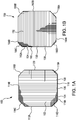
- FIGS. 1A and 1B illustrate, respectively, examples of first and second types of solar cells in accordance with the invention.
- FIG. 1A is a top plan view of a semiconductor solar cell 100 of the first type.
- the solar cell 100 which can be scribed or cut out from a substantially circular semiconductor wafer at the end of a fabrication process, can have a substantially rectangular shape.
- the solar cell 100 has two parallel long side edges 112A, 112B opposite one another, and two parallel short side edges 114A, 114B opposite one another.
- the longer side edges 112A, 112B are substantially perpendicular to the shorter side edges 114A, 114B.
- adjacent side edges of the solar cell may not form right-angles with one another; instead, the corners 116A, 116B, 116C, 116D of the solar cell 100 may appear as cut-off or rounded. The result is that the solar cell 100 may not be perfectly rectangular-shaped.
- one or more electrical contacts 104, 106, 108 are provided along one of the short side edges 114A at the top surface of the cell 100.
- Vertical conductors 102 extend in parallel over the top surface of the cell 100 and function to make electrical contact with the top layer of the cell and collect charge when the surface is illuminated. Thus, the conductors 102 extend substantially in parallel with the long side edges 112A, 112B.
- the top surface of the cell 100 also includes an electrically conducting bus 110, which extends along the periphery of the cell 100 at the short side edge 114A and at the corners 116A, 116D.
- the bus 110 functions to electrically connect each of the conductors 102, and also to connect to the electrical contacts 104, 106, 108 on the top surface of the cell 100.
- the bottom surface of the solar cell 100 can be covered substantially entirely with a metallic layer so as to serve as a lower, or bottom surface (i.e., backside), metallic contact for the cell 100.
- the solar cell is an n-on-p device.
- the top surface (as shown in FIG. 1A ) serves as the cathode, whereas the bottom or backside surface serves as the anode.
- the solar cell 100 can be, for example, a III-V multi-junction solar cell that includes a bottom cell, a middle cell and a top cell. Other implementations may use a different arrangement for the solar cell 100.
- FIG. 1B is a top plan view of a semiconductor solar cell 150 of the second type
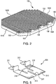
- FIG. 2 is a perspective view of the same solar cell.
- the solar cell 150 of the second type can be similar to the solar cell 100 of the first type.
- the solar cell 150 can have two parallel long side edges 162A, 162B opposite one another, and two parallel short side edges 164A, 164B opposite one another.
- the longer side edges 162A, 162B are substantially perpendicular to the shorter side edges 164A, 164B.
- the overall shape and dimensions of the solar cell 150 can be substantially the same as the shape and dimensions of the solar cell 100.
- adjacent side edges of the solar cell 150 may not form right-angles with one another; instead, the corners 166A, 166B, 166C, 166D of the solar cell 150 may appear as cut-off or rounded. The result is that the solar cell 150 may not be perfectly rectangular-shaped.
- the second type of solar cell 150 also includes one or more electrical contacts 154, 156, 158 at the top surface of the cell 100.
- the contacts 104, 106, 108 for the solar cell 100 of FIG. 1A are provided along one of the short side edges 114A
- the contacts 154, 156, 158 for the solar cell 150 of FIG. 1B are provided along one of the long side edges 162A.
- Horizontal conductors 152 extend in parallel over the top surface of the cell 150 and function to make electrical contact with the top layer of the cell and collect charge when the surface is illuminated.
- the conductors 152 extend substantially in parallel with the short side edges 164A, 164B.
- the top surface of the cell 150 also includes an electrically conducting bus 160, which extends along the periphery of the cell 100 at the long side edge 162A and at the corners 166C, 166D.
- the bus 110 functions to electrically connect each of the conductors 152, and also to connect to the electrical contacts 154, 156, 158 on the top surface of the cell 150.
- the bottom surface of the solar cell 150 can be covered substantially entirely with a metallic layer so as to serve as a lower, or bottom surface (i.e., backside), metallic contact for the cell 150.
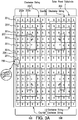
- FIG. 3A illustrates multiple solar cell arrays 200, 300, 400, 500 each of which includes solar cells of two different types, A and B.
- solar cells of type A correspond to the solar cell 100 of FIG. 1A
- solar cells of type B correspond to the solar cell 150 of FIG. 1B .
- the cells of each particular array (e.g., array 200) are arranged in a series connection and are supported, for example, by a lower substrate.
- the surface of the substrate on which the cells of a particular array are supported can include a periphery and an interior region.
- the series connection for the array 200 includes a first solar cell 201a whose bottom surface anode is connected to the top surface cathode contact(s) of the next adjacent cell 201b.
- the series connection of cells in the array 200 follows a clockwise spiral-type shape winding path 204 that starts with the first cell 201a at the periphery of the surface of the support substrate and ends with the last cell 203 disposed at the interior area of the surface of the support substrate.
- the support substrate is usually a composite material with an aluminum honeycomb core.
- the bottom surface anode of the cell 201b is connected to the top surface cathode contact(s) of the next adjacent 201c.
- the series connection continues in this fashion such that the bottom surface anode of each cell (other than the last cell 203) is connected to the top surface cathode contact(s) of the next adjacent cell.
- the electrical contacts on the next cell when connecting the bottom surface of one cell in the series to the electrical contacts on the top surface of the next cell, it is desirable for the electrical contacts on the next cell to be located at the side edge of that cell that is closest to a side edge of the previous cell.
- the next cell when a connection is made from one cell to a next cell in the same column, the next cell is of type A, which has electrical contacts on one of its short side edges (i.e., the short side edge that is adjacent to the previous cell).
- the next cell when a connection is made from one cell to a next cell in the same row, the next cell is of type B, which has electrical contacts on one of its longer side edges (i.e., the long side edge that is adjacent to the previous cell).
- the next cell when a connection is made from one cell to a next cell in the same row, the next cell is of type B, which has electrical contacts on one of its long side edges (i.e., the long side edge that is adjacent to the previous cell).
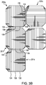
- FIG. 3B which shows a partial, enlarged version of the some of the cells 201e, 201f, 201g, 202a in the upper left-hand section of the array 200, illustrates the relative positioning of the cells and their top surface contacts.
- the cell 201e and the next cell 201f are both of type A, and the top surface contacts 104, 106, 108 of the cell 201f are located at its lower side edge, which is adjacent the top side edge of the cell 201e.
- this allows the two cells 201e, 201f to be connected electrically by an interconnect 600 that connects the metalized bottom surface of the cell 201e to one or more of the top surface contacts of the cell 201f.
- the metallized bottom surface of the cell 201f can be connected by an interconnect 600 in a similar fashion to one or more of the top surface contacts of the next cell 201g, which also is of type A.
- the cell 201g in the upper left-hand corner of the array 200 is of type A
- the next cell 202a is of type B
- the top surface contacts 154, 156, 158 of the cell 202a are located at its left-hand side edge, which is adjacent the right-hand side edge of the cell 201g.
- this allows the two cells 201g, 202a to be connected electrically by an interconnect 600 that connects the metalized bottom surface of the cell 201g to one or more of the top surface contacts of the cell 202a.
- the metallized bottom surface of the cell 202a can be connected by an interconnect 600 in a similar manner to one or more of the top surface contacts of the next cell 202b, which also is of type B.
- FIG. 5 illustrates further details of the interconnect 600 according to some implementations.
- the interconnect 600 can include, for example, first and second flat contact members 310, 311 that extend outward for contact, respectively, with two of the top surface contacts on one of the solar cells.
- the flat contact members 310, 311 should be spaced from one another at a distance that is the same as the distance between adjacent top surface contacts (e.g., contacts 104, 106 of the cell 201e; or contacts 156, 158 of the cell 202a).
- An advantage of providing two separate contact members and two top surface contacts is to achieve improved reliability in the event one of the electrical contacts is broken or otherwise shorts.
- the interconnect 600 is serpentine shaped, with middle portions 312, 313 for electrical contact with the metal layer on the bottom surface of one of the solar cells.
- the interconnect 600 can include one or more gaps 317, 318, where the planar surface changes direction, for stress relief. The details of the interconnect 600 may differ in other implementations.
- each array (e.g., array 200) includes a first terminal electrically connected directly to the first cell 201a in the series connection, and a second terminal electrically connected directly to a last cell 203 in the series connection.
- the first terminal connected to the first cell 201a is a lower voltage terminal of negative (-) polarity
- the second terminal connected to the last cell 203 is a higher voltage terminal of positive (+) polarity.
- the second terminal can be disposed at an interior area of the array that is sufficiently distant from the first terminal so as to reduce occurrence of electrostatic discharge. In some cases, the second terminal may be disposed at or near the center of the array, although in other instances, this need not be the case.
- a feed-through hole for the positive (+) terminal can be provided through the support substrate on which the cells of the array are supported.
- the series connection of the cells of the array 200 are arranged along a clockwise spiral-type path, in other arrays, the series connection of the cells can be arranged along a counterclockwise spiral-type path (see, e.g., arrays 300 and 400).
- each array of FIG. 2A (e.g., array 200) are arranged in columns and rows, different configurations may be used for other implementations.
- the array may include multiple rows, where the cells in a particular row are slightly offset or staggered from the cells of an adjacent row.
- the array may include multiple columns, where the cells in a particular column are slightly offset or staggered from the cells of an adjacent column.
- each array can depend on the particular needs of the application for the solar cell array. In some implementations, there are at least twenty-seven cells, each of which provides about a two-volt increase. More generally, however, the array can include a greater or lesser number of cells.
- Multiple solar cell arrays can be combined and connected electrically to form a solar cell panel.
- four sub-arrays 200, 300, 400, 500 are provided to form a single panel.
- the negative (-) terminal of each of the sub-arrays 200, 300, 400, 500 can be connected to a common cathode bus 700.
- Each of the arrays 300, 400, 500 can be similar to the array 200 as described above.
- the series connection of the cells in each particular array 200, 300, 400, 500 may follow a clockwise spiral-type shape winding path.
- the series connection of the cells in each particular array 200, 300, 400, 500 may follow a counterclockwise spiral-type shape winding path.
- some of the arrays in the panel have a clockwise spiral-type shape winding path, whereas other ones of the arrays have a counterclockwise spiral-type shape winding path.
- each sub-array 200, 500 having a clockwise spiral-type path is adjacent only sub-arrays 300, 400 having a counterclockwise spiral-type path.
- FIG. 3A shows a panel having four sub-arrays 200, 300, 400, 500, other implementations can include fewer or more arrays.
Landscapes
- Photovoltaic Devices (AREA)
Description
- The present disclosure relates to the field of solar cell arrays.
- Photovoltaic cells, also known as solar cells, are one of the most important new devices for producing electrical energy that has become commercially competitive with other energy sources over the past several years. Considerable effort has gone into increasing the solar conversion efficiency of solar cells. As a result, solar cells are currently being used in a number of commercial and consumer-oriented applications. While significant progress has been made in this area, the requirement for solar cells to meet the needs of more sophisticated applications has not kept pace with demand. Applications such as satellites used in data communications, for example, have dramatically increased the demand for solar cells with improved power and energy conversion characteristics.
- Solar cells often are fabricated from semiconductor wafers in vertical, multifunction structures, and the wafers or cells are laid out in a planar array, with the individual solar cells connected together in columns in a series electrical current. The shape and structure of the columns forming the array, as well as the number of cells it contains, are determined in part by the desired output voltage and current.
- Designing solar cell arrays presents a wide range of challenges. Moreover, competing engineering goals can be difficult to achieve in a single design. For example, it generally is desirable to provide a compact arrangement for the solar cells. This can be particularly important, for example, for satellite and other space related applications. On the other hand, a compact design can, in some cases, exacerbate other problems. For example, when differently-charged objects (e.g., negative and positive terminals of the solar cell array) are located close together, the buildup of electrostatic discharge (ESD) between the two objects can generate an electric spark. Such an ESD event can result in serious damage, for example, to a satellite's solar cells, and the satellite may suffer significant power loss. Thus, it is desirable to protect solar cell arrays, located for example on spacecraft, from sparking caused by electrostatic discharge.
-
US-2013/0019919-A1 discloses an arrangement based on solar cells having a substantially rectangular shape with cropped corners, and an upper surface featuring collector bars extending at least along one longer side and one shorter side of the solar cell. - The present disclosure describes solar cell arrays that include multiple cells connected to one another in series on a surface. The array includes first and second different types of solar cells. Incorporating two different types of cells can facilitate various layouts of the cells in the array, including compact arrangements. In some implementations, the use of two different types of cells can allow arrangements in which voltage terminals of opposite polarity to be disposed at a sufficiently large distance from one another so as to help reduce the occurrence of ESD.
- In one aspect, for example, a solar cell device includes an array of solar cells disposed on a surface region having a periphery and an interior area. Each cell in the array has a top side and a bottom side, two long side edges opposite one another, and two short side edges opposite one another. The array includes cells of a first type and cells of a second different type. Each cell of the first type has metallization on its bottom side and one or more electrical contacts on its top side adjacent one of its short side edges.
- Each cell of the second type has metallization on its bottom side and one or more electrical contacts on its top side adjacent one of its long side edges. The cells in the array are connected to one another in series. The solar cell device further includes a first terminal electrically connected directly to a first cell in the series connection, and a second terminal electrically connected directly to a last cell in the series connection. The first cell is disposed at the periphery, and the last cell is disposed at the interior area.
- Some implementations include one or more of the following features. For example, the cells can be connected in series from the first cell to the last cell along a clockwise or counterclockwise winding path. In some case, the winding path has a spiral-type shape. In some instances, the first terminal is a lower voltage terminal of negative polarity, and the second terminal is a higher voltage terminal of positive polarity. Preferably, the second terminal is disposed at a location in the interior area that is sufficiently distant from the first terminal so as to reduce occurrence of electrostatic discharge.
- According to another aspect, a solar cell panel can include multiple arrays of solar cells each of which can be configured as described above. Different ones of the arrays can have their cells arranged, for example, in a series connection along a clockwise or counterclockwise path so as to achieve cancellation of magnetic moments generated by currents in the arrays.
- Other aspects, features and advantages will be apparent from the following detailed description, the accompanying drawings and the claims.
-
-
FIG. 1A is a top plan view of a first type of solar cell. -
FIG. 1B is a top plan view of a second type of solar cell. -
FIG. 2 shows additional details of the solar cell ofFIG. 1B . -
FIG. 3A illustrates an example of a solar cell panel. -
FIG. 3B shows further details of a portion ofFIG. 3A . -
FIG. 4A illustrates an example of two interconnected solar cells. -
FIG. 4B illustrates another example of two interconnected solar cells. -
FIG. 5 illustrates an example of an interconnect member for connecting two adjacent solar cells electrically to one another. - Broadly speaking, the present disclosure describes solar cell arrays that include multiple cells connected to one another in series on a surface. The array includes first and second different types of solar cells. Incorporating two different types of cells can facilitate various layouts of the cells in the array, including compact arrangements. The use of two different types of cells also can allow arrangements in which voltage terminals of opposite polarity, which are connected, respectively, to the first and last cells in the series, to be disposed at a sufficient distance from one another so as to help reduce the occurrence of ESD. For example, a first cell in the series connection can be disposed at the periphery of array, whereas a last cell in the series connection can be disposed, for example, at an interior area of the array.
-
FIGS. 1A and 1B illustrate, respectively, examples of first and second types of solar cells in accordance with the invention.FIG. 1A is a top plan view of a semiconductorsolar cell 100 of the first type. Thesolar cell 100, which can be scribed or cut out from a substantially circular semiconductor wafer at the end of a fabrication process, can have a substantially rectangular shape. In the illustrated example, thesolar cell 100 has two parallel long side edges 112A, 112B opposite one another, and two parallel short side edges 114A, 114B opposite one another. The longer side edges 112A, 112B are substantially perpendicular to the shorter side edges 114A, 114B. In order to maximize the amount of each circular wafer that is used to form the solar cell, adjacent side edges of the solar cell may not form right-angles with one another; instead, thecorners solar cell 100 may appear as cut-off or rounded. The result is that thesolar cell 100 may not be perfectly rectangular-shaped. - As further illustrated in
FIG. 1A , one or moreelectrical contacts short side edges 114A at the top surface of thecell 100.Vertical conductors 102 extend in parallel over the top surface of thecell 100 and function to make electrical contact with the top layer of the cell and collect charge when the surface is illuminated. Thus, theconductors 102 extend substantially in parallel with the long side edges 112A, 112B. The top surface of thecell 100 also includes an electrically conductingbus 110, which extends along the periphery of thecell 100 at theshort side edge 114A and at thecorners bus 110 functions to electrically connect each of theconductors 102, and also to connect to theelectrical contacts cell 100. The bottom surface of thesolar cell 100 can be covered substantially entirely with a metallic layer so as to serve as a lower, or bottom surface (i.e., backside), metallic contact for thecell 100. - In the illustrated example, the solar cell is an n-on-p device. Thus, the top surface (as shown in
FIG. 1A ) serves as the cathode, whereas the bottom or backside surface serves as the anode. Thesolar cell 100 can be, for example, a III-V multi-junction solar cell that includes a bottom cell, a middle cell and a top cell. Other implementations may use a different arrangement for thesolar cell 100. -
FIG. 1B is a top plan view of a semiconductorsolar cell 150 of the second type, andFIG. 2 is a perspective view of the same solar cell. In many respects, thesolar cell 150 of the second type can be similar to thesolar cell 100 of the first type. Thus, thesolar cell 150 can have two parallel long side edges 162A, 162B opposite one another, and two parallel short side edges 164A, 164B opposite one another. The longer side edges 162A, 162B are substantially perpendicular to the shorter side edges 164A, 164B. The overall shape and dimensions of thesolar cell 150 can be substantially the same as the shape and dimensions of thesolar cell 100. Here too, adjacent side edges of thesolar cell 150 may not form right-angles with one another; instead, thecorners solar cell 150 may appear as cut-off or rounded. The result is that thesolar cell 150 may not be perfectly rectangular-shaped. - As further illustrated in
FIGS. 1B and2 , the second type ofsolar cell 150 also includes one or moreelectrical contacts cell 100. However, whereas thecontacts solar cell 100 ofFIG. 1A are provided along one of the short side edges 114A, thecontacts solar cell 150 ofFIG. 1B are provided along one of the long side edges 162A. -
Horizontal conductors 152 extend in parallel over the top surface of thecell 150 and function to make electrical contact with the top layer of the cell and collect charge when the surface is illuminated. Theconductors 152 extend substantially in parallel with the short side edges 164A, 164B. The top surface of thecell 150 also includes an electrically conductingbus 160, which extends along the periphery of thecell 100 at thelong side edge 162A and at thecorners bus 110 functions to electrically connect each of theconductors 152, and also to connect to theelectrical contacts cell 150. The bottom surface of thesolar cell 150 can be covered substantially entirely with a metallic layer so as to serve as a lower, or bottom surface (i.e., backside), metallic contact for thecell 150. -
FIG. 3A illustrates multiplesolar cell arrays solar cell 100 ofFIG. 1A , whereas solar cells of type B correspond to thesolar cell 150 ofFIG. 1B . The cells of each particular array (e.g., array 200) are arranged in a series connection and are supported, for example, by a lower substrate. The surface of the substrate on which the cells of a particular array are supported can include a periphery and an interior region. - Returning to the example of
FIG. 3A , the series connection for thearray 200 includes a firstsolar cell 201a whose bottom surface anode is connected to the top surface cathode contact(s) of the nextadjacent cell 201b. In the illustrated example, the series connection of cells in thearray 200 follows a clockwise spiral-typeshape winding path 204 that starts with thefirst cell 201a at the periphery of the surface of the support substrate and ends with thelast cell 203 disposed at the interior area of the surface of the support substrate. The support substrate is usually a composite material with an aluminum honeycomb core. Thus, the bottom surface anode of thecell 201b is connected to the top surface cathode contact(s) of the next adjacent 201c. The series connection continues in this fashion such that the bottom surface anode of each cell (other than the last cell 203) is connected to the top surface cathode contact(s) of the next adjacent cell. - In general, when connecting the bottom surface of one cell in the series to the electrical contacts on the top surface of the next cell, it is desirable for the electrical contacts on the next cell to be located at the side edge of that cell that is closest to a side edge of the previous cell. Thus, in the example of
FIG. 2A , when a connection is made from one cell to a next cell in the same column, the next cell is of type A, which has electrical contacts on one of its short side edges (i.e., the short side edge that is adjacent to the previous cell). On the other hand, when a connection is made from one cell to a next cell in the same row, the next cell is of type B, which has electrical contacts on one of its longer side edges (i.e., the long side edge that is adjacent to the previous cell). Thus, in the example ofFIG. 2A , when a connection is made from one cell to a next cell in the same row, the next cell is of type B, which has electrical contacts on one of its long side edges (i.e., the long side edge that is adjacent to the previous cell). -
FIG. 3B , which shows a partial, enlarged version of the some of thecells array 200, illustrates the relative positioning of the cells and their top surface contacts. For example, thecell 201e and thenext cell 201f are both of type A, and thetop surface contacts cell 201f are located at its lower side edge, which is adjacent the top side edge of thecell 201e. As illustrated inFIG. 4A , this allows the twocells interconnect 600 that connects the metalized bottom surface of thecell 201e to one or more of the top surface contacts of thecell 201f. The metallized bottom surface of thecell 201f can be connected by aninterconnect 600 in a similar fashion to one or more of the top surface contacts of thenext cell 201g, which also is of type A. - On the other hand, as further shown in
FIG. 3B , thecell 201g in the upper left-hand corner of thearray 200, is of type A, whereas thenext cell 202a is of type B. Thetop surface contacts cell 202a are located at its left-hand side edge, which is adjacent the right-hand side edge of thecell 201g. As further illustrated inFIG. 4B , this allows the twocells interconnect 600 that connects the metalized bottom surface of thecell 201g to one or more of the top surface contacts of thecell 202a. The metallized bottom surface of thecell 202a can be connected by aninterconnect 600 in a similar manner to one or more of the top surface contacts of thenext cell 202b, which also is of type B. -
FIG. 5 illustrates further details of theinterconnect 600 according to some implementations. Theinterconnect 600 can include, for example, first and secondflat contact members flat contact members contacts cell 201e; orcontacts cell 202a). An advantage of providing two separate contact members and two top surface contacts is to achieve improved reliability in the event one of the electrical contacts is broken or otherwise shorts. Theinterconnect 600 ofFIG. 5 is serpentine shaped, withmiddle portions interconnect 600 can include one ormore gaps interconnect 600 may differ in other implementations. - As shown in
FIG. 3A , each array (e.g., array 200) includes a first terminal electrically connected directly to thefirst cell 201a in the series connection, and a second terminal electrically connected directly to alast cell 203 in the series connection. In the illustrated example, the first terminal connected to thefirst cell 201a is a lower voltage terminal of negative (-) polarity, and the second terminal connected to thelast cell 203 is a higher voltage terminal of positive (+) polarity. The second terminal can be disposed at an interior area of the array that is sufficiently distant from the first terminal so as to reduce occurrence of electrostatic discharge. In some cases, the second terminal may be disposed at or near the center of the array, although in other instances, this need not be the case. A feed-through hole for the positive (+) terminal can be provided through the support substrate on which the cells of the array are supported. - Although the series connection of the cells of the
array 200 are arranged along a clockwise spiral-type path, in other arrays, the series connection of the cells can be arranged along a counterclockwise spiral-type path (see, e.g.,arrays 300 and 400). - Further, although the cells of each array of
FIG. 2A (e.g., array 200) are arranged in columns and rows, different configurations may be used for other implementations. For example, the array may include multiple rows, where the cells in a particular row are slightly offset or staggered from the cells of an adjacent row. Likewise, the array may include multiple columns, where the cells in a particular column are slightly offset or staggered from the cells of an adjacent column. - The number of solar cells in each array (e.g., array 200) can depend on the particular needs of the application for the solar cell array. In some implementations, there are at least twenty-seven cells, each of which provides about a two-volt increase. More generally, however, the array can include a greater or lesser number of cells.
- Multiple solar cell arrays can be combined and connected electrically to form a solar cell panel. For example, as shown in
FIG. 2A , four sub-arrays 200, 300, 400, 500 are provided to form a single panel. In this case, the negative (-) terminal of each of the sub-arrays 200, 300, 400, 500 can be connected to acommon cathode bus 700. Each of thearrays array 200 as described above. In some cases, the series connection of the cells in eachparticular array particular array FIG. 2A , which shows sub-arrays 200 and 500 having clockwise spiral-type paths, and sub-arrays 300, 400 with counterclockwise spiral-type paths. Thus, in the illustrated example, each sub-array 200, 500 having a clockwise spiral-type path is adjacent only sub-arrays 300, 400 having a counterclockwise spiral-type path. - Although
FIG. 3A shows a panel having foursub-arrays - Other implementations are within the scope of the claims.
Claims (14)
- A solar cell device comprising:an array of solar cells (150, 160), wherein the cells are disposed on a surface region having a periphery and an interior area, each cell in the array having a top side and a bottom side, two long side edges (112A, 112B; 162A, 162B) opposite one another, and two short side edges (114A, 114B, 164A, 164B) opposite one another,wherein the array includes:cells of a first type (A) each of which has metallization on its bottom side and which has one or more electrical contacts (104, 106, 108) on its top side adjacent one of its short side edges (114A) and not adjacent the other one of its short side edges (114B) and not adjacent any of its long side edges (112A, 112B), andcells (160) of a second different type (B) each of which has metallization on its bottom side and which has one or more electrical contacts (154, 156, 158) on its top side adjacent one of its long side edges (162A) and not adjacent the other one of its long side edges (162B) and not adjacent any of its short side edges (164A, 164B),wherein the cells in the array are connected to one another in series;the solar cell device further including:a first terminal electrically connected directly to a first cell (201a) in the series connection, wherein the first cell is disposed at the periphery; anda second terminal electrically connected directly to a last cell (203) in the series connection, wherein the last cell is disposed at the interior area.
- The solar cell device of claim 1 wherein the cells are connected in series from the first cell (201a) to the last cell (203) along a clockwise or counterclockwise winding path.
- The solar cell device of claim 2 wherein the winding path has a spiral-type shape.
- The solar cell device of claim 2 wherein the first terminal is a lower voltage terminal of negative polarity, and the second terminal is a higher voltage terminal of positive polarity.
- The solar cell device of claim 4 wherein the second terminal is disposed at a location in the interior area that is sufficiently distant from the first terminal so as to reduce occurrence of electrostatic discharge.
- The solar cell device of claim 1 wherein, other than for the last cell in the series connection, the metallization on the bottom side of each particular cell is connected to one or more of the contacts (104, 106, 108; 154, 156, 158) on the top side of a next adjacent cell.
- The solar cell device of claim 6 wherein the metallization on the bottom side of each cell is a first electrode of a first polarity, and wherein the one or more contacts on the top side of each cell are a second electrode of a second opposite polarity.
- The solar cell device of claim 1 wherein the series connection of cells includes multiple transitions from a cell of the first type (A) to a next cell of the second type (B), and multiple transitions from a cell of the second type (B) to a next cell of the first type (A).
- The solar cell device of claim 1 wherein the cells of the array are arranged in rows and columns.
- The solar cell device of claim 1 wherein the surface region has a through-hole for connecting the second terminal to the last cell.
- The solar cell device of any of the preceding claims, wherein said one or more electrical contacts (104, 106, 108; 154, 156, 158) are electrically connected to an electrically conducting bus (110, 160).
- The solar cell device according to claim 11, wherein in cells of the first type (A), the electrically conducting bus extends along the periphery of the solar cell at a short side edge (114A) and corresponding corners (116A, 116D) of the solar cell, and wherein in the cells of the second type (B), the electrically conducting bus extends along the periphery of the solar cell at a long side edge (162A) and corresponding corners (166C, 166D) of the solar cell.
- The solar cell device of any of claims 11 and 12 wherein the cells of the first type (A) further comprise conductors (102) that extend in parallel over the top surface of the respective cell (100) and are arranged to make electrical contact with a top layer of the respective cell and collect charge when the surface is illuminated, whereby the conductors (102) extend substantially in parallel with the long side edges (112A, 112B) of the respective cell, the electrically conducting bus (110) being electrically connected to each of the conductors (102).
- The solar cell device of any of claims 11-13 wherein the cells of the second type (B) further comprise conductors (152) that extend in parallel over the top surface of the respective cell (150) and are arranged to make electrical contact with a top layer of the respective cell and collect charge when the surface is illuminated, whereby the conductors (152) extend substantially in parallel with the short side edges (164A, 164B) of the respective cell, the electrically conducting bus (160) being electrically connected to each of the conductors (152).
Applications Claiming Priority (1)
| Application Number | Priority Date | Filing Date | Title |
|---|---|---|---|
| US14/151,236 US20150194551A1 (en) | 2014-01-09 | 2014-01-09 | Solar cell array having two different types of cells |
Publications (3)
| Publication Number | Publication Date |
|---|---|
| EP2894676A2 EP2894676A2 (en) | 2015-07-15 |
| EP2894676A3 EP2894676A3 (en) | 2015-08-26 |
| EP2894676B1 true EP2894676B1 (en) | 2021-05-19 |
Family
ID=52232107
Family Applications (1)
| Application Number | Title | Priority Date | Filing Date |
|---|---|---|---|
| EP15150388.5A Active EP2894676B1 (en) | 2014-01-09 | 2015-01-07 | Solar cell array having two different types of cells |
Country Status (2)
| Country | Link |
|---|---|
| US (1) | US20150194551A1 (en) |
| EP (1) | EP2894676B1 (en) |
Families Citing this family (13)
| Publication number | Priority date | Publication date | Assignee | Title |
|---|---|---|---|---|
| USD765590S1 (en) * | 2013-12-11 | 2016-09-06 | Solaero Technologies Corp. | Solar cell |
| USD765024S1 (en) * | 2013-12-11 | 2016-08-30 | Solaero Technologies Corp. | Solar cell |
| US10370766B2 (en) | 2016-10-27 | 2019-08-06 | The Regents Of The University Of California | Hybrid photo-electrochemical and photo-voltaic cells |
| USD804059S1 (en) * | 2016-10-28 | 2017-11-28 | Solarcity Corporation | Photovoltaic roof tile |
| US11575058B2 (en) | 2017-06-30 | 2023-02-07 | Mitsubishi Electric Corporation | Solar power generator, solar array wing, and space structure |
| TWI661572B (en) * | 2017-07-21 | 2019-06-01 | 海力雅集成股份有限公司 | Solar module and the manufacture thereof |
| USD838667S1 (en) * | 2017-10-16 | 2019-01-22 | Flex Ltd. | Busbar-less solar cell |
| USD839180S1 (en) * | 2017-10-31 | 2019-01-29 | Flex Ltd. | Busbar-less solar cell |
| JP1659059S (en) * | 2019-03-08 | 2020-05-11 | ||
| USD909961S1 (en) * | 2019-06-06 | 2021-02-09 | Grouphug, Inc. | Solar panel assembly |
| CN111725344B (en) * | 2020-06-29 | 2022-04-08 | 阳光新能源开发股份有限公司 | A photovoltaic module and photovoltaic array |
| CN111900225B (en) * | 2020-06-30 | 2021-11-16 | 上海空间电源研究所 | A space solar cell array interconnection structure, solar cell array and forming method thereof |
| US12256577B2 (en) * | 2020-10-05 | 2025-03-18 | Kaneka Corporation | Solar cell |
Family Cites Families (13)
| Publication number | Priority date | Publication date | Assignee | Title |
|---|---|---|---|---|
| IT1239117B (en) * | 1988-11-01 | 1993-09-28 | Gen Electric | ANTIELECTROSTATIC SOLAR PANEL |
| JPH08204220A (en) * | 1995-01-31 | 1996-08-09 | Mitsubishi Electric Corp | Solar cell, solar cell module, and solar cell module group |
| US6248950B1 (en) * | 1998-02-21 | 2001-06-19 | Space Systems/Loral, Inc. | Solar array augmented electrostatic discharge for spacecraft in geosynchronous earth orbit |
| JPH11238897A (en) * | 1998-02-23 | 1999-08-31 | Canon Inc | Solar cell module manufacturing method and solar cell module |
| FR2822436B1 (en) * | 2001-03-21 | 2003-08-15 | Cit Alcatel | SOLAR PANEL HAVING ELECTRICAL TERMINALS DISTRIBUTED ON ITS SURFACE |
| JP5153097B2 (en) * | 2006-07-31 | 2013-02-27 | 三洋電機株式会社 | Solar cell module |
| EP2232577A1 (en) * | 2007-12-18 | 2010-09-29 | Day4 Energy Inc. | Photovoltaic module with edge access to pv strings, interconnection method, apparatus, and system |
| US20110011439A1 (en) * | 2008-02-25 | 2011-01-20 | Masatomo Hasegawa | Photovoltaic power system |
| TWI493732B (en) * | 2009-02-17 | 2015-07-21 | Shinetsu Chemical Co | Solar module |
| CA2763065A1 (en) * | 2009-05-25 | 2010-12-02 | Day4 Energy Inc. | Photovoltaic module string arrangement and shading protection therefor |
| US20120318319A1 (en) * | 2011-06-17 | 2012-12-20 | Solopower, Inc. | Methods of interconnecting thin film solar cells |
| US9000288B2 (en) * | 2011-07-22 | 2015-04-07 | Space Systems/Loral, Llc | Current collector bar and grid pattern for a photovoltaic solar cell |
| WO2013106896A1 (en) * | 2012-01-17 | 2013-07-25 | Day4 Energy Inc. | Photovoltaic module with cell assemblies bearing adhesive for securing the assemblies in the module |
-
2014
- 2014-01-09 US US14/151,236 patent/US20150194551A1/en not_active Abandoned
-
2015
- 2015-01-07 EP EP15150388.5A patent/EP2894676B1/en active Active
Non-Patent Citations (1)
| Title |
|---|
| None * |
Also Published As
| Publication number | Publication date |
|---|---|
| US20150194551A1 (en) | 2015-07-09 |
| EP2894676A3 (en) | 2015-08-26 |
| EP2894676A2 (en) | 2015-07-15 |
Similar Documents
| Publication | Publication Date | Title |
|---|---|---|
| EP2894676A2 (en) | Solar cell array having two different types of cells | |
| US9960292B2 (en) | Radially arranged metal contact fingers for solar cells | |
| TWI656649B (en) | Photovoltaic module | |
| CN104205347A (en) | Photovoltaic module comprising shingled photovoltaic tiles and manufacturing process thereof | |
| WO2013044114A1 (en) | Architectures for solid state batteries | |
| CN106165117B (en) | Backside contact layer for photovoltaic modules with improved cell connection topology | |
| US8796534B2 (en) | Solar cell and assembly of a plurality of solar cells | |
| KR20190013952A (en) | Photocell assemblies, photovoltaic arrays, and solar cell assemblies | |
| CN111448672B (en) | Solar cell with junction retracted from cut edge | |
| US20240170594A1 (en) | Solar cell string and method for producing a solar cell string | |
| US20180190847A1 (en) | Non-orthogonally patterned monolithically integrated thin film pv | |
| EP2854183A1 (en) | Back contact solar cell | |
| US12495622B2 (en) | Solar-cell module | |
| US12414383B2 (en) | Thin film photo-voltaic module | |
| JP6871044B2 (en) | Solar cell module | |
| KR102026101B1 (en) | Solar Cell Module And Solar Cell Array Using Thereof | |
| CN106165118B (en) | For the backside contact layer of the PV modules with bypass configuration | |
| JP7265655B1 (en) | solar module | |
| EP3058596B1 (en) | Assembly of photovoltaic cells and fabrication thereof | |
| JP7711116B2 (en) | Solar Cell Module | |
| CN111584660A (en) | Photovoltaic module and photovoltaic device including the same | |
| CN117059687A (en) | solar panel | |
| CN116759480A (en) | Solar cell modules and battery components |
Legal Events
| Date | Code | Title | Description |
|---|---|---|---|
| PUAI | Public reference made under article 153(3) epc to a published international application that has entered the european phase |
Free format text: ORIGINAL CODE: 0009012 |
|
| 17P | Request for examination filed |
Effective date: 20150107 |
|
| AK | Designated contracting states |
Kind code of ref document: A2 Designated state(s): AL AT BE BG CH CY CZ DE DK EE ES FI FR GB GR HR HU IE IS IT LI LT LU LV MC MK MT NL NO PL PT RO RS SE SI SK SM TR |
|
| AX | Request for extension of the european patent |
Extension state: BA ME |
|
| PUAL | Search report despatched |
Free format text: ORIGINAL CODE: 0009013 |
|
| AK | Designated contracting states |
Kind code of ref document: A3 Designated state(s): AL AT BE BG CH CY CZ DE DK EE ES FI FR GB GR HR HU IE IS IT LI LT LU LV MC MK MT NL NO PL PT RO RS SE SI SK SM TR |
|
| AX | Request for extension of the european patent |
Extension state: BA ME |
|
| RIC1 | Information provided on ipc code assigned before grant |
Ipc: H01L 31/05 20140101AFI20150721BHEP |
|
| R17P | Request for examination filed (corrected) |
Effective date: 20160225 |
|
| RBV | Designated contracting states (corrected) |
Designated state(s): AL AT BE BG CH CY CZ DE DK EE ES FI FR GB GR HR HU IE IS IT LI LT LU LV MC MK MT NL NO PL PT RO RS SE SI SK SM TR |
|
| STAA | Information on the status of an ep patent application or granted ep patent |
Free format text: STATUS: EXAMINATION IS IN PROGRESS |
|
| 17Q | First examination report despatched |
Effective date: 20180418 |
|
| GRAP | Despatch of communication of intention to grant a patent |
Free format text: ORIGINAL CODE: EPIDOSNIGR1 |
|
| STAA | Information on the status of an ep patent application or granted ep patent |
Free format text: STATUS: GRANT OF PATENT IS INTENDED |
|
| INTG | Intention to grant announced |
Effective date: 20210127 |
|
| GRAS | Grant fee paid |
Free format text: ORIGINAL CODE: EPIDOSNIGR3 |
|
| GRAA | (expected) grant |
Free format text: ORIGINAL CODE: 0009210 |
|
| STAA | Information on the status of an ep patent application or granted ep patent |
Free format text: STATUS: THE PATENT HAS BEEN GRANTED |
|
| AK | Designated contracting states |
Kind code of ref document: B1 Designated state(s): AL AT BE BG CH CY CZ DE DK EE ES FI FR GB GR HR HU IE IS IT LI LT LU LV MC MK MT NL NO PL PT RO RS SE SI SK SM TR |
|
| REG | Reference to a national code |
Ref country code: GB Ref legal event code: FG4D |
|
| REG | Reference to a national code |
Ref country code: CH Ref legal event code: EP |
|
| REG | Reference to a national code |
Ref country code: DE Ref legal event code: R096 Ref document number: 602015069361 Country of ref document: DE |
|
| REG | Reference to a national code |
Ref country code: AT Ref legal event code: REF Ref document number: 1394841 Country of ref document: AT Kind code of ref document: T Effective date: 20210615 |
|
| REG | Reference to a national code |
Ref country code: IE Ref legal event code: FG4D |
|
| REG | Reference to a national code |
Ref country code: LT Ref legal event code: MG9D |
|
| REG | Reference to a national code |
Ref country code: AT Ref legal event code: MK05 Ref document number: 1394841 Country of ref document: AT Kind code of ref document: T Effective date: 20210519 |
|
| REG | Reference to a national code |
Ref country code: NL Ref legal event code: MP Effective date: 20210519 |
|
| PG25 | Lapsed in a contracting state [announced via postgrant information from national office to epo] |
Ref country code: BG Free format text: LAPSE BECAUSE OF FAILURE TO SUBMIT A TRANSLATION OF THE DESCRIPTION OR TO PAY THE FEE WITHIN THE PRESCRIBED TIME-LIMIT Effective date: 20210819 Ref country code: AT Free format text: LAPSE BECAUSE OF FAILURE TO SUBMIT A TRANSLATION OF THE DESCRIPTION OR TO PAY THE FEE WITHIN THE PRESCRIBED TIME-LIMIT Effective date: 20210519 Ref country code: LT Free format text: LAPSE BECAUSE OF FAILURE TO SUBMIT A TRANSLATION OF THE DESCRIPTION OR TO PAY THE FEE WITHIN THE PRESCRIBED TIME-LIMIT Effective date: 20210519 Ref country code: FI Free format text: LAPSE BECAUSE OF FAILURE TO SUBMIT A TRANSLATION OF THE DESCRIPTION OR TO PAY THE FEE WITHIN THE PRESCRIBED TIME-LIMIT Effective date: 20210519 Ref country code: HR Free format text: LAPSE BECAUSE OF FAILURE TO SUBMIT A TRANSLATION OF THE DESCRIPTION OR TO PAY THE FEE WITHIN THE PRESCRIBED TIME-LIMIT Effective date: 20210519 |
|
| PG25 | Lapsed in a contracting state [announced via postgrant information from national office to epo] |
Ref country code: RS Free format text: LAPSE BECAUSE OF FAILURE TO SUBMIT A TRANSLATION OF THE DESCRIPTION OR TO PAY THE FEE WITHIN THE PRESCRIBED TIME-LIMIT Effective date: 20210519 Ref country code: SE Free format text: LAPSE BECAUSE OF FAILURE TO SUBMIT A TRANSLATION OF THE DESCRIPTION OR TO PAY THE FEE WITHIN THE PRESCRIBED TIME-LIMIT Effective date: 20210519 Ref country code: NO Free format text: LAPSE BECAUSE OF FAILURE TO SUBMIT A TRANSLATION OF THE DESCRIPTION OR TO PAY THE FEE WITHIN THE PRESCRIBED TIME-LIMIT Effective date: 20210819 Ref country code: PL Free format text: LAPSE BECAUSE OF FAILURE TO SUBMIT A TRANSLATION OF THE DESCRIPTION OR TO PAY THE FEE WITHIN THE PRESCRIBED TIME-LIMIT Effective date: 20210519 Ref country code: PT Free format text: LAPSE BECAUSE OF FAILURE TO SUBMIT A TRANSLATION OF THE DESCRIPTION OR TO PAY THE FEE WITHIN THE PRESCRIBED TIME-LIMIT Effective date: 20210920 Ref country code: ES Free format text: LAPSE BECAUSE OF FAILURE TO SUBMIT A TRANSLATION OF THE DESCRIPTION OR TO PAY THE FEE WITHIN THE PRESCRIBED TIME-LIMIT Effective date: 20210519 Ref country code: GR Free format text: LAPSE BECAUSE OF FAILURE TO SUBMIT A TRANSLATION OF THE DESCRIPTION OR TO PAY THE FEE WITHIN THE PRESCRIBED TIME-LIMIT Effective date: 20210820 Ref country code: LV Free format text: LAPSE BECAUSE OF FAILURE TO SUBMIT A TRANSLATION OF THE DESCRIPTION OR TO PAY THE FEE WITHIN THE PRESCRIBED TIME-LIMIT Effective date: 20210519 Ref country code: IS Free format text: LAPSE BECAUSE OF FAILURE TO SUBMIT A TRANSLATION OF THE DESCRIPTION OR TO PAY THE FEE WITHIN THE PRESCRIBED TIME-LIMIT Effective date: 20210919 |
|
| PG25 | Lapsed in a contracting state [announced via postgrant information from national office to epo] |
Ref country code: NL Free format text: LAPSE BECAUSE OF FAILURE TO SUBMIT A TRANSLATION OF THE DESCRIPTION OR TO PAY THE FEE WITHIN THE PRESCRIBED TIME-LIMIT Effective date: 20210519 |
|
| PG25 | Lapsed in a contracting state [announced via postgrant information from national office to epo] |
Ref country code: RO Free format text: LAPSE BECAUSE OF FAILURE TO SUBMIT A TRANSLATION OF THE DESCRIPTION OR TO PAY THE FEE WITHIN THE PRESCRIBED TIME-LIMIT Effective date: 20210519 Ref country code: SM Free format text: LAPSE BECAUSE OF FAILURE TO SUBMIT A TRANSLATION OF THE DESCRIPTION OR TO PAY THE FEE WITHIN THE PRESCRIBED TIME-LIMIT Effective date: 20210519 Ref country code: SK Free format text: LAPSE BECAUSE OF FAILURE TO SUBMIT A TRANSLATION OF THE DESCRIPTION OR TO PAY THE FEE WITHIN THE PRESCRIBED TIME-LIMIT Effective date: 20210519 Ref country code: EE Free format text: LAPSE BECAUSE OF FAILURE TO SUBMIT A TRANSLATION OF THE DESCRIPTION OR TO PAY THE FEE WITHIN THE PRESCRIBED TIME-LIMIT Effective date: 20210519 Ref country code: CZ Free format text: LAPSE BECAUSE OF FAILURE TO SUBMIT A TRANSLATION OF THE DESCRIPTION OR TO PAY THE FEE WITHIN THE PRESCRIBED TIME-LIMIT Effective date: 20210519 Ref country code: DK Free format text: LAPSE BECAUSE OF FAILURE TO SUBMIT A TRANSLATION OF THE DESCRIPTION OR TO PAY THE FEE WITHIN THE PRESCRIBED TIME-LIMIT Effective date: 20210519 |
|
| REG | Reference to a national code |
Ref country code: DE Ref legal event code: R097 Ref document number: 602015069361 Country of ref document: DE |
|
| PLBE | No opposition filed within time limit |
Free format text: ORIGINAL CODE: 0009261 |
|
| STAA | Information on the status of an ep patent application or granted ep patent |
Free format text: STATUS: NO OPPOSITION FILED WITHIN TIME LIMIT |
|
| 26N | No opposition filed |
Effective date: 20220222 |
|
| PG25 | Lapsed in a contracting state [announced via postgrant information from national office to epo] |
Ref country code: IS Free format text: LAPSE BECAUSE OF FAILURE TO SUBMIT A TRANSLATION OF THE DESCRIPTION OR TO PAY THE FEE WITHIN THE PRESCRIBED TIME-LIMIT Effective date: 20210919 Ref country code: AL Free format text: LAPSE BECAUSE OF FAILURE TO SUBMIT A TRANSLATION OF THE DESCRIPTION OR TO PAY THE FEE WITHIN THE PRESCRIBED TIME-LIMIT Effective date: 20210519 |
|
| PG25 | Lapsed in a contracting state [announced via postgrant information from national office to epo] |
Ref country code: IT Free format text: LAPSE BECAUSE OF FAILURE TO SUBMIT A TRANSLATION OF THE DESCRIPTION OR TO PAY THE FEE WITHIN THE PRESCRIBED TIME-LIMIT Effective date: 20210519 |
|
| PG25 | Lapsed in a contracting state [announced via postgrant information from national office to epo] |
Ref country code: MC Free format text: LAPSE BECAUSE OF FAILURE TO SUBMIT A TRANSLATION OF THE DESCRIPTION OR TO PAY THE FEE WITHIN THE PRESCRIBED TIME-LIMIT Effective date: 20210519 |
|
| REG | Reference to a national code |
Ref country code: CH Ref legal event code: PL |
|
| GBPC | Gb: european patent ceased through non-payment of renewal fee |
Effective date: 20220107 |
|
| REG | Reference to a national code |
Ref country code: BE Ref legal event code: MM Effective date: 20220131 |
|
| PG25 | Lapsed in a contracting state [announced via postgrant information from national office to epo] |
Ref country code: LU Free format text: LAPSE BECAUSE OF NON-PAYMENT OF DUE FEES Effective date: 20220107 Ref country code: GB Free format text: LAPSE BECAUSE OF NON-PAYMENT OF DUE FEES Effective date: 20220107 |
|
| PG25 | Lapsed in a contracting state [announced via postgrant information from national office to epo] |
Ref country code: BE Free format text: LAPSE BECAUSE OF NON-PAYMENT OF DUE FEES Effective date: 20220131 |
|
| PG25 | Lapsed in a contracting state [announced via postgrant information from national office to epo] |
Ref country code: LI Free format text: LAPSE BECAUSE OF NON-PAYMENT OF DUE FEES Effective date: 20220131 Ref country code: CH Free format text: LAPSE BECAUSE OF NON-PAYMENT OF DUE FEES Effective date: 20220131 |
|
| PG25 | Lapsed in a contracting state [announced via postgrant information from national office to epo] |
Ref country code: IE Free format text: LAPSE BECAUSE OF NON-PAYMENT OF DUE FEES Effective date: 20220107 |
|
| PG25 | Lapsed in a contracting state [announced via postgrant information from national office to epo] |
Ref country code: HU Free format text: LAPSE BECAUSE OF FAILURE TO SUBMIT A TRANSLATION OF THE DESCRIPTION OR TO PAY THE FEE WITHIN THE PRESCRIBED TIME-LIMIT; INVALID AB INITIO Effective date: 20150107 |
|
| PG25 | Lapsed in a contracting state [announced via postgrant information from national office to epo] |
Ref country code: MK Free format text: LAPSE BECAUSE OF FAILURE TO SUBMIT A TRANSLATION OF THE DESCRIPTION OR TO PAY THE FEE WITHIN THE PRESCRIBED TIME-LIMIT Effective date: 20210519 Ref country code: CY Free format text: LAPSE BECAUSE OF FAILURE TO SUBMIT A TRANSLATION OF THE DESCRIPTION OR TO PAY THE FEE WITHIN THE PRESCRIBED TIME-LIMIT Effective date: 20210519 |
|
| PG25 | Lapsed in a contracting state [announced via postgrant information from national office to epo] |
Ref country code: MT Free format text: LAPSE BECAUSE OF FAILURE TO SUBMIT A TRANSLATION OF THE DESCRIPTION OR TO PAY THE FEE WITHIN THE PRESCRIBED TIME-LIMIT Effective date: 20210519 |
|
| REG | Reference to a national code |
Ref country code: DE Ref legal event code: R079 Ref document number: 602015069361 Country of ref document: DE Free format text: PREVIOUS MAIN CLASS: H01L0031050000 Ipc: H10F0019900000 |
|
| PG25 | Lapsed in a contracting state [announced via postgrant information from national office to epo] |
Ref country code: TR Free format text: LAPSE BECAUSE OF FAILURE TO SUBMIT A TRANSLATION OF THE DESCRIPTION OR TO PAY THE FEE WITHIN THE PRESCRIBED TIME-LIMIT Effective date: 20210519 |
|
| PGFP | Annual fee paid to national office [announced via postgrant information from national office to epo] |
Ref country code: FR Payment date: 20251208 Year of fee payment: 12 |
|
| PGFP | Annual fee paid to national office [announced via postgrant information from national office to epo] |
Ref country code: DE Payment date: 20251203 Year of fee payment: 12 |