EP2894661A1 - Directly bonded, lattice-mismatched semiconductor device - Google Patents
Directly bonded, lattice-mismatched semiconductor device Download PDFInfo
- Publication number
- EP2894661A1 EP2894661A1 EP15150677.1A EP15150677A EP2894661A1 EP 2894661 A1 EP2894661 A1 EP 2894661A1 EP 15150677 A EP15150677 A EP 15150677A EP 2894661 A1 EP2894661 A1 EP 2894661A1
- Authority
- EP
- European Patent Office
- Prior art keywords
- bonding layer
- substrate
- subassembly
- lattice
- mismatched
- Prior art date
- Legal status (The legal status is an assumption and is not a legal conclusion. Google has not performed a legal analysis and makes no representation as to the accuracy of the status listed.)
- Granted
Links
Images



Classifications
-
- H—ELECTRICITY
- H10—SEMICONDUCTOR DEVICES; ELECTRIC SOLID-STATE DEVICES NOT OTHERWISE PROVIDED FOR
- H10F—INORGANIC SEMICONDUCTOR DEVICES SENSITIVE TO INFRARED RADIATION, LIGHT, ELECTROMAGNETIC RADIATION OF SHORTER WAVELENGTH OR CORPUSCULAR RADIATION
- H10F10/00—Individual photovoltaic cells, e.g. solar cells
- H10F10/10—Individual photovoltaic cells, e.g. solar cells having potential barriers
- H10F10/16—Photovoltaic cells having only PN heterojunction potential barriers
- H10F10/161—Photovoltaic cells having only PN heterojunction potential barriers comprising multiple PN heterojunctions, e.g. tandem cells
-
- H—ELECTRICITY
- H10—SEMICONDUCTOR DEVICES; ELECTRIC SOLID-STATE DEVICES NOT OTHERWISE PROVIDED FOR
- H10F—INORGANIC SEMICONDUCTOR DEVICES SENSITIVE TO INFRARED RADIATION, LIGHT, ELECTROMAGNETIC RADIATION OF SHORTER WAVELENGTH OR CORPUSCULAR RADIATION
- H10F10/00—Individual photovoltaic cells, e.g. solar cells
- H10F10/10—Individual photovoltaic cells, e.g. solar cells having potential barriers
- H10F10/14—Photovoltaic cells having only PN homojunction potential barriers
- H10F10/144—Photovoltaic cells having only PN homojunction potential barriers comprising only Group III-V materials, e.g. GaAs,AlGaAs, or InP photovoltaic cells
-
- H—ELECTRICITY
- H10—SEMICONDUCTOR DEVICES; ELECTRIC SOLID-STATE DEVICES NOT OTHERWISE PROVIDED FOR
- H10F—INORGANIC SEMICONDUCTOR DEVICES SENSITIVE TO INFRARED RADIATION, LIGHT, ELECTROMAGNETIC RADIATION OF SHORTER WAVELENGTH OR CORPUSCULAR RADIATION
- H10F19/00—Integrated devices, or assemblies of multiple devices, comprising at least one photovoltaic cell covered by group H10F10/00, e.g. photovoltaic modules
- H10F19/40—Integrated devices, or assemblies of multiple devices, comprising at least one photovoltaic cell covered by group H10F10/00, e.g. photovoltaic modules comprising photovoltaic cells in a mechanically stacked configuration
-
- H—ELECTRICITY
- H10—SEMICONDUCTOR DEVICES; ELECTRIC SOLID-STATE DEVICES NOT OTHERWISE PROVIDED FOR
- H10F—INORGANIC SEMICONDUCTOR DEVICES SENSITIVE TO INFRARED RADIATION, LIGHT, ELECTROMAGNETIC RADIATION OF SHORTER WAVELENGTH OR CORPUSCULAR RADIATION
- H10F71/00—Manufacture or treatment of devices covered by this subclass
-
- H—ELECTRICITY
- H10—SEMICONDUCTOR DEVICES; ELECTRIC SOLID-STATE DEVICES NOT OTHERWISE PROVIDED FOR
- H10F—INORGANIC SEMICONDUCTOR DEVICES SENSITIVE TO INFRARED RADIATION, LIGHT, ELECTROMAGNETIC RADIATION OF SHORTER WAVELENGTH OR CORPUSCULAR RADIATION
- H10F71/00—Manufacture or treatment of devices covered by this subclass
- H10F71/139—Manufacture or treatment of devices covered by this subclass using temporary substrates
-
- H—ELECTRICITY
- H10—SEMICONDUCTOR DEVICES; ELECTRIC SOLID-STATE DEVICES NOT OTHERWISE PROVIDED FOR
- H10P—GENERIC PROCESSES OR APPARATUS FOR THE MANUFACTURE OR TREATMENT OF DEVICES COVERED BY CLASS H10
- H10P10/00—Bonding of wafers, substrates or parts of devices
- H10P10/12—Bonding of semiconductor wafers or semiconductor substrates to semiconductor wafers or semiconductor substrates
- H10P10/128—Bonding of semiconductor wafers or semiconductor substrates to semiconductor wafers or semiconductor substrates by direct semiconductor to semiconductor bonding
-
- Y—GENERAL TAGGING OF NEW TECHNOLOGICAL DEVELOPMENTS; GENERAL TAGGING OF CROSS-SECTIONAL TECHNOLOGIES SPANNING OVER SEVERAL SECTIONS OF THE IPC; TECHNICAL SUBJECTS COVERED BY FORMER USPC CROSS-REFERENCE ART COLLECTIONS [XRACs] AND DIGESTS
- Y02—TECHNOLOGIES OR APPLICATIONS FOR MITIGATION OR ADAPTATION AGAINST CLIMATE CHANGE
- Y02E—REDUCTION OF GREENHOUSE GAS [GHG] EMISSIONS, RELATED TO ENERGY GENERATION, TRANSMISSION OR DISTRIBUTION
- Y02E10/00—Energy generation through renewable energy sources
- Y02E10/50—Photovoltaic [PV] energy
- Y02E10/544—Solar cells from Group III-V materials
-
- Y—GENERAL TAGGING OF NEW TECHNOLOGICAL DEVELOPMENTS; GENERAL TAGGING OF CROSS-SECTIONAL TECHNOLOGIES SPANNING OVER SEVERAL SECTIONS OF THE IPC; TECHNICAL SUBJECTS COVERED BY FORMER USPC CROSS-REFERENCE ART COLLECTIONS [XRACs] AND DIGESTS
- Y02—TECHNOLOGIES OR APPLICATIONS FOR MITIGATION OR ADAPTATION AGAINST CLIMATE CHANGE
- Y02E—REDUCTION OF GREENHOUSE GAS [GHG] EMISSIONS, RELATED TO ENERGY GENERATION, TRANSMISSION OR DISTRIBUTION
- Y02E10/00—Energy generation through renewable energy sources
- Y02E10/50—Photovoltaic [PV] energy
- Y02E10/547—Monocrystalline silicon PV cells
-
- Y—GENERAL TAGGING OF NEW TECHNOLOGICAL DEVELOPMENTS; GENERAL TAGGING OF CROSS-SECTIONAL TECHNOLOGIES SPANNING OVER SEVERAL SECTIONS OF THE IPC; TECHNICAL SUBJECTS COVERED BY FORMER USPC CROSS-REFERENCE ART COLLECTIONS [XRACs] AND DIGESTS
- Y02—TECHNOLOGIES OR APPLICATIONS FOR MITIGATION OR ADAPTATION AGAINST CLIMATE CHANGE
- Y02P—CLIMATE CHANGE MITIGATION TECHNOLOGIES IN THE PRODUCTION OR PROCESSING OF GOODS
- Y02P70/00—Climate change mitigation technologies in the production process for final industrial or consumer products
- Y02P70/50—Manufacturing or production processes characterised by the final manufactured product
Definitions
- the disclosed system and method relate to a semiconductor device and, more particularly, to a directly bonded, lattice-mismatched semiconductor device.
- Wafer joining technology may be used to integrate various properties from different materials into one compact process-compatible material system. Wafer joining technology has great potential. For example, joining GaAs or InP-based materials to other semiconductor materials may result in the integration of optical, photovoltaic, and electronic devices and enhance the performance of computers, solar cells, light emitting diodes and other electronic devices.
- Group III-V semiconductor materials are comprised of one or more elements from Group III of the periodic table and one or more elements from Group V of the periodic table.
- One of the limitations of Group III-V semiconductor devices, such as multi-junction solar cells, is the need to incorporate various lattice-matched device components within a semiconductor device. Specifically, lattice-matching may limit the possible bandgap combinations between device components in the semiconductor device. Thus, in an effort to expand or widen the bandgap combinations between various device components within a semiconductor device, inverted metamorphic (IMM) technologies may be employed to grow device components that are lattice-mismatched to their growth substrate.
- IMM inverted metamorphic
- IMM technologies may invert the usual growth order of device components, where the lattice-mismatched device components may be grown last.
- multiple transparent buffer layers may be used to absorb the strain of the lattice-mismatch between various device components.
- incorporating multiple transparent buffer layers may increase the cost of the semiconductor device.
- the resulting semiconductor device grown using IMM technologies may require an additional device handle, which also adds cost to the semiconductor device.
- lattice-matched materials of specific bandgap combinations may be directly bonded to one another.
- a sacrificial lateral etch layer and an epitaxial lift-off process may be employed to recycle the growth substrate in an effort to reduce cost.
- Some examples of the growth substrate include GaAs-based, InP-based, and GaSb-based materials.
- a semiconductor device including a first subassembly and a second subassembly.
- the first subassembly may include a first bonding layer and a first substrate.
- the second subassembly may include a second substrate and a second bonding layer that may be directly bonded to the first bonding layer.
- the first bonding layer and the second bonding layer may be lattice-mismatched with one another. At least one of the following may be selected: the first bonding layer is lattice-mismatched to the first substrate, and the second bonding layer is lattice-mismatched to the second substrate
- a method of making a semiconductor device may include providing a first subassembly comprising a first bonding layer and a first substrate. The method may also include providing a second subassembly comprising a second substrate and a second bonding layer. The method may also include directly bonding the first bonding layer and the second bonding layer together. The first bonding layer and the second bonding layer may be lattice-mismatched to one another. At least one of the following is selected: the first bonding layer may be lattice-mismatched to the first substrate, and the second bonding layer is lattice-mismatched to the second substrate.
- a semiconductor device comprising: a first subassembly comprising a first bonding layer and a first substrate; and a second subassembly, comprising: a second substrate; and a second bonding layer directly bonded to the first bonding layer, wherein the first bonding layer and the second bonding layer are lattice-mismatched to one another, and wherein at least one of the following is selected: the first bonding layer is lattice-mismatched to the first substrate, and the second bonding layer is lattice-mismatched to the second substrate.
- the second bonding layer is lattice-mismatched to the second substrate.
- a buffer layer is epitaxially grown on the second substrate.
- the second substrate is constructed of germanium (Ge).
- the second substrate includes an active Ge subcell.
- the second subassembly includes semiconductor layers lattice-mismatched to the second substrate.
- the first bonding layer is lattice-mismatched to the first substrate.
- the first subassembly includes first semiconductor layers lattice-matched to the first substrate.
- the first subassembly includes a buffer layer epitaxially grown on the first semiconductor layers.
- the first subassembly includes second semiconductor layers lattice-mismatched to the first substrate.
- the second semiconductor layers are epitaxially grown on the buffer layer.
- At least one of the first subassembly and the second subassembly includes one of a photovoltaic device and a solar cell.
- a method of making a semiconductor device comprising; providing a first subassembly comprising a first bonding layer and a first substrate; providing a second subassembly comprising a second substrate and a second bonding layer; directly bonding the first bonding layer and the second bonding layer together, wherein the first bonding layer and the second bonding layer are lattice-mismatched to one another; and selecting at least one of the following: lattice-mismatching the first bonding layer to the first substrate, and lattice-mismatching the second bonding layer to the second substrate.
- the method includes selecting lattice-mismatching the second bonding layer to the second substrate, and epitaxially growing a buffer layer on the second substrate.
- the method comprises constructing the second substrate of germanium (Ge).
- the method comprises creating an active Ge subcell within the second substrate by a diffusion of dopants into a layer of the second substrate.
- the method comprises epitaxially growing first semiconductor layers upon the first substrate of the first subassembly, wherein the first semiconductor layers are lattice-matched to the first substrate.
- the method comprises epitaxially growing a buffer layer upon the first semiconductor layers.
- the method comprises epitaxially growing second semiconductor layers on the buffer layer, wherein the second semiconductor layers are lattice-mismatched to the first substrate, and wherein the first bonding layer is lattice-mismatched to the first substrate.
- a preassembled structure 100 may include a first subassembly 102 and a second subassembly 104.
- the first subassembly 102 may include a first wafer 110 and a first bonding layer 120 directly adjacent and upon a first surface 110a of the first wafer 110.
- the first wafer 110 may be a semiconductor selected from group III-V materials.
- the first wafer 110 may be selected from the group consisting of silicon (Si), germanium (Ge), GaAs-based, InP-based, GaP based, GaSb-based, Ga(In)N-based materials.
- the first surface 110a of the first wafer 110 may be a surface of a material layer selected from the group consisting of silicon (Si), germanium (Ge), Gallium Arsenide (GaAs), Indium Phosphide (InP), Gallium Phosphide (GaP), Gallium Antimonide (GaSb), Gallium Indium Arsenide (GaInAs), Gallium Indium Phosphide (GaInP), Gallium Indium Nitride Ga(In)N materials.
- the first bonding layer 120 may be epitaxially grown upon the first surface 110a of the first wafer 110.
- the first bonding layer 120 may be an (Al)(Ga)InP(As)(Sb) material having a relatively high dopant concentration equal to or greater than about 5 x 10 18 /cm 3 . It is to be understood that a relatively high doping concentration may not be necessary for sufficient mechanical bonding, but may be needed for achieving a low electrical resistance across a bonded interface (shown in FIG. 2 as a bonded interface 150). However, if a low electrical resistance across the bonded interface 150 is not required, then a relatively high doping concentration in the first bonding layer 120 may not be necessary.
- the use of parentheses in the (Al)(Ga)InP(As)(Sb) material indicates that the incorporation of aluminum, gallium, arsenic, and antimony is optional.
- the first bonding layer 120 may be lattice-matched to the first wafer 110, and may include a first bonding surface 120a.
- the second subassembly 104 may include a second wafer 130, an optional buffer layer, and a second bonding layer 140.
- the second bonding layer 140 may be directly adjacent and upon a second surface 130a of the second wafer 130.
- the second wafer 130 may be a Ge substrate wafer.
- the second wafer 130 may be constructed of other materials as well such as, for example, GaAs.
- the second wafer 130 may be used as a growth substrate as well as for structural support. Specifically, the second wafer 130 may be used as a substrate for epitaxial growth of the second bonding layer 140 as well as the main mechanical support for an assembled semiconductor device 200 (shown in FIG. 2 ).
- the second wafer 130 may include an active Ge subcell 134.
- the Ge subcell 134 may be omitted.
- the Ge subcell 134 may include an energy bandgap of about 0.67 eV.
- the Ge subcell 134 may be created by a diffusion of dopants into a surface layer of the second wafer 130. In other words, the Ge subcell 134 may not be epitaxially grown. Thus, the Ge subcell may be part of the second wafer 130.
- the second bonding layer 140 may be epitaxially grown upon the second surface 130a of the second wafer 130. Similar to the first bonding layer 120, in one embodiment the second bonding layer 140 may also be an (Al)(Ga)InP(As)(Sb) material having a relatively high dopant concentration equal to or greater than about 5x10 18 /cm 3 . It is to be understood that a relatively high doping concentration may not be necessary for sufficient mechanical bonding, but may be needed for achieving a low electrical resistance across the bonded interface (shown in FIG. 2 as the bonded interface 150). However, if a low electrical resistance across the bonded interface is not required, then a relatively high doping concentration in the second bonding layer 140 may not be necessary.
- the second bonding layer 140 may be lattice-matched to the second wafer 130 of the second subassembly 104.
- the second bonding layer 140 may also be lattice-mismatched to the second wafer 130 as well, and are described in detail below and illustrated in FIGS. 4-9 .
- the second bonding layer 140 of the second subassembly 104 may be lattice-mismatched to the first bonding layer 120 of the first subassembly 102.
- the first bonding layer 120 and the second bonding layer 140 may be lattice-mismatched to one another.
- FIG. 2 is an illustration of the semiconductor device 200 according to an embodiment of the disclosure, where the first bonding layer 120 and the second bonding layer 140 have been bonded together to join the first subassembly 102 to the second subassembly 104.
- the semiconductor device 200 may be a photovoltaic device, a solar cell, a light sensor, light emitting diode, or a transistor.
- the first subassembly 102 and the second subassembly 104 may be directly bonded to one another by placing the first bonding layer 120 and the second bonding layer 140 in direct contact with one another, where heat and pressure may be applied to bond the first subassembly 102 and the second subassembly 104 together.
- the first bonding surface 120a and a second bonding surface 140a may be placed in contact with one another, and diffuse together to form the bonded interface 150.
- the first bonding surface 120a and the second bonding surface 140a may be polished prior to bringing the first bonding layer 120 and the second bonding layer 140 into contact.
- the polishing may be performed by Chemical Mechanical Polishing (CMP), with bonding performed using conventional wafer bonding equipment.
- CMP Chemical Mechanical Polishing
- the first subassembly 102 and the second subassembly 104 may be heated to a bonding temperature of between about 300°C to about 500°C.
- the semiconductor device 200 may be heated at a pressure of between about 20 psi and about 50 psi.
- the semiconductor device 200 may be heated under pressure for about 20 to 300 minutes.
- Direct semiconductor bonding with (Al)GaInP(As)(Sb) bonding layers has achieved bond strength greater than 4.1 J/m 2 , electrical resistance as low as 0.3 Ohm-cm 2 and optical transparency of greater than 97% across a bonded interface (e.g., the bonded interface 150 as shown in FIG. 2 ). After direct bonding, the first wafer 110 may be removed.
- FIG. 3 illustrates an exemplary process flow diagram of a method 300 for creating the semiconductor device 200 as shown in FIG. 2 .
- method 300 may begin at block 302, where the first bonding layer 120 may be epitaxially grown upon the first surface 110a of the first wafer 110 of the first subassembly 102. As discussed above, the first bonding layer 120 may be lattice-matched to the first wafer 110. Method 300 may then proceed to block 304.
- the second bonding layer 140 may be epitaxially grown upon the second surface 130a of the second wafer 130 of the second subassembly 104. As discussed above, the second bonding layer 140 may be lattice-matched to the second wafer 130. However the second bonding layer 140 of the second subassembly 104 may be lattice-mismatched to the first bonding layer 120 of the first subassembly 102. Method 300 may then proceed to block 306. In block 306, the first subassembly 102 and the second subassembly 104 may be directly bonded to one another at the first bonding surface 120a and the second bonding surface 140a, thus creating the semiconductor device 200 (shown in FIG. 2 ).
- first bonding surface 120a and the second bonding surface 140a may be placed in contact with one another, and heated to the bonding temperature.
- the first bonding layer 120 and the second bonding layers 140 diffuse together to form the bonded interface 150 (seen in FIG. 2 ).
- Method 300 may then terminate.
- FIG. 4 illustrates an alternative embodiment of preassembled structure 400 according to an embodiment of the disclosure.
- the preassembled structure 400 may include a first subassembly 402 and a second subassembly 404.
- the first subassembly 402 may include a first wafer 410, semiconductor layers 412, and a first bonding layer 420.
- the semiconductor layers 412 may be directly adjacent and upon a first surface 410a of the first wafer 410.
- the semiconductor layers 412 may be a photovoltaic device, or a solar cell having one or more subcells.
- the first bonding layer 420 may be directly adjacent and upon a semiconductor surface 412a of the semiconductor layers 412. Similar to the embodiment as described above and shown in FIGS.
- the first wafer 410 may be a semiconductor selected from group III-V materials.
- the first wafer 410 may be selected from the group consisting of silicon (Si), germanium (Ge), Gallium Arsenide (GaAs), Indium Phosphide (InP), Gallium Phosphide (GaP), Gallium Antimonide (GaSb), Gallium Indium Arsenide (GaInAs), Gallium Indium Phosphide (GaInP), Gallium Indium Nitride Ga(In)N materials.
- the semiconductor layers 412 may be epitaxially grown upon the first surface 410a of the first wafer 410.
- the semiconductor layers 412 may be lattice-matched to the first wafer 410.
- the first bonding layer 420 may be epitaxially grown upon the semiconductor surface 412a of the semiconductor layers 412. Similar to the embodiment as shown in FIGS. 1-3 and described above, the first bonding layer 420 may be an (Al)(Ga)InP(As)(Sb) material, and in one embodiment may have a relatively high dopant concentration equal to or greater than about 5 x 10 18 /cm 3 .
- the first bonding layer 420 may also be lattice-matched to the first wafer 410, and may include a first bonding surface 420a.
- the second subassembly 404 may include a second wafer 430, a buffer layer 432, semiconductor layers 436, and a second bonding layer 440.
- the buffer layer 432 may be directly adjacent and upon a second surface 430a of the second wafer 430.
- the semiconductor layers 436 may be directly adjacent and upon a buffer surface 432a of the buffer layer 432.
- the second bonding layer 440 may be directly adjacent and upon a semiconductor surface 436a of the semiconductor layers 436.
- the second wafer 430 may be a Ge substrate, and may be used as a growth substrate as well as for structural support. Specifically, the second wafer 430 may be used as a substrate for epitaxial growth of the buffer layer 432 as well the main mechanical support for an assembled semiconductor device 500 (shown in FIG. 5 ). The buffer layer 432 may be epitaxially grown upon the second surface 430a of the second wafer 430. In one embodiment, the second wafer 430 may include an active Ge subcell 434. However, it is to be understood that in some embodiments, the Ge subcell 434 may be omitted.
- the buffer layer 432 may be epitaxially grown upon the second surface 430a of the second wafer 430.
- the buffer layer 432 may be a metamorphic transparent graded buffer. In the embodiments as described, the term transparent may be defined as a transmission of equal to or greater than about ninety-seven percent of the light or electromagnetic radiation of a wavelength for activating a cell or subcell disposed underneath.
- the buffer layer 432 may be used to epitaxially grow material that is lattice-mismatched to the second wafer 430.
- the buffer layer 432 may be used to grow the semiconductor layers 436.
- the semiconductor layers 436 may be lattice-mismatched to the second wafer 430.
- the buffer layer 432 may absorb the strain of lattice-mismatch, and generally prevents the vertical propagation of dislocations.
- the second bonding layer 440 may be epitaxially grown upon the semiconductor surface 436a of the semiconductor layers 436.
- the second bonding layer 440 may include a second bonding surface 440a. Similar to the first bonding layer 420, the second bonding layer 440 may be an (Al)(Ga)InP(As)(Sb) material, and may have a relatively high dopant concentration equal to or greater than about 5 x 10 18 /cm 3 .
- both the semiconductor layers 436 and the second bonding layer 440 of the second subassembly 404 may be lattice-mismatched to the second wafer 430.
- the second bonding layer 440 may be lattice-matched to the semiconductor layers 436.
- the first bonding layer 420 of the first subassembly 402 may be lattice-mismatched to the second bonding layer 440 of the second subassembly 404.
- FIG. 5 is an illustration of the semiconductor device 500 according to an embodiment of the disclosure, where the first bonding layer 420 and the second bonding layer 440 have been bonded together to join the first subassembly 402 to the second subassembly 404.
- the first subassembly 402 and the second subassembly 404 may be directly bonded to one another by placing the first bonding layer 420 and the second bonding layer 440 in direct contact with one another, where heat and pressure may be applied to bond the first subassembly 402 and the second subassembly 404 together.
- the first bonding surface 420a and the second bonding surface 440a may be placed in contact with one another, and diffuse together to form the bonded interface 450.
- FIG. 6 illustrates an exemplary process flow diagram of a method 600 for creating the semiconductor device 500 as shown in FIG. 5 .
- the method 600 may begin at block 602, where the semiconductor layers 412 and the first bonding layer 420 may be epitaxially grown upon the first wafer 410 of the first subassembly 402. Specifically, the semiconductor layers 412 may be grown upon the first surface 410a of the first wafer 410, and the first bonding layer 420 may be epitaxially grown upon the semiconductor surface 412a of the semiconductor layers 412. Method 600 may then proceed to block 604.
- the buffer layer 432 may be epitaxially grown upon the second surface 430a of the second wafer 430 of the second subassembly 404. Method 600 may then proceed to block 606.
- the semiconductor layers 436 may be epitaxially grown upon the buffer surface 432a of the buffer layer 432 of the second subassembly 404. As described above, the semiconductor layers 436 may be lattice-mismatched to the second wafer 430. Method 600 may then proceed to block 608.
- the second bonding layer 440 may be epitaxially grown upon the semiconductor surface 436a of the semiconductor layers 436 of the second subassembly 404. As discussed above, the second bonding layer 440 may be lattice-mismatched to the second wafer 430. The second bonding layer 440 may also be lattice-mismatched to the first bonding layer 420 of the first subassembly 402. Method 600 may then proceed to block 610.
- the first subassembly 402 and the second subassembly 404 may be directly bonded to one another at the first bonding surface 420a and the second bonding surface 440a, thus creating the semiconductor device 500 (shown in FIG. 5 ).
- the first bonding surface 420a and the second bonding surface 440a FIG. 4
- the first bonding layer 420 and the second bonding layer 440 diffuse together to form the bonded interface 450 (seen in FIG. 5 ).
- Method 600 may then terminate.
- FIG. 7 illustrates an alternative embodiment of preassembled structure 700 according to an embodiment of the disclosure.
- the preassembled structure 700 may include a first subassembly 702 and a second subassembly 704.
- the first subassembly 702 may include a first wafer 710, first semiconductor layers 712, a buffer layer 714, second semiconductor layers 716, and a first bonding layer 720.
- the first semiconductor layers 712 may be directly adjacent and upon a first surface 710a of the first wafer 710.
- the first semiconductor layers 712 may be a photovoltaic device, or a solar cell having one or more subcells.
- the buffer layer 714 may be epitaxially grown upon a first semiconductor surface 712a of the first semiconductor layers 712.
- the buffer layer 714 may also be a metamorphic transparent graded buffer.
- the second semiconductor layers 716 may be directly adjacent and upon a buffer surface 714a of the buffer layer 714.
- the second semiconductor layers 716 may also be a photovoltaic device, or a solar cell having one or more subcells.
- the first bonding layer 720 may be directly adjacent and upon a second semiconductor surface 716a of the second semiconductor layers 716.
- the first wafer 710 may be a semiconductor selected from group III-V materials.
- the first wafer 710 may be selected from the group consisting of silicon (Si), germanium (Ge), Gallium Arsenide (GaAs), Indium Phosphide (InP), Gallium Phosphide (GaP), Gallium Antimonide (GaSb), , Gallium Indium Arsenide (GaInAs), Gallium Indium Phosphide (GaInP), Gallium Indium Nitride Ga(In)N materials.
- the first semiconductor layers 712 may be epitaxially grown upon the first surface 710a of the first wafer 710, and may be lattice-matched to the first wafer 710.
- the buffer layer 714 may be epitaxially grown upon the first semiconductor surface 712a of the first semiconductor layer 712.
- the buffer layer 714 may be used to epitaxially grow material that is lattice-mismatched to the first wafer 710.
- the buffer layer 714 may be used to grow the second semiconductor layers 716, which may be lattice-mismatched to the first wafer 710.
- the first bonding layer 720 may be epitaxially grown upon the second semiconductor surface 716a of the second semiconductor layers 716. Similar to the embodiment as shown in FIGS. 1-6 and described above, the first bonding layer 720 may be an (Al)(Ga)InP(As)(Sb) material, and in one embodiment may have a relatively high dopant concentration equal to or greater than about 5 x 10 18 g/cm 3 . In the embodiment as shown in FIG. 7 , the first bonding layer 720 may be lattice-mismatched to the first wafer 710 and lattice-matched to the second semiconductor layers 716, and may include a first bonding surface 720a.
- the second subassembly 704 may include a second wafer 730, a buffer layer 732, semiconductor layers 736, and a second bonding layer 740.
- the buffer layer 732 may be directly adjacent and upon a second surface 730a of the second wafer 730.
- the semiconductor layers 736 may be directly adjacent and upon a buffer surface 732a of the buffer layer 732.
- the second bonding layer 740 may be directly adjacent and upon a semiconductor surface 736a of the semiconductor layers 736.
- the second wafer 730 may be a Ge substrate, and may be used as a growth substrate as well as for structural support. Specifically, the second wafer 730 may be used as a substrate for epitaxial growth of the buffer layer 732, as well as the main mechanical support for an assembled semiconductor device 800 (shown in FIG. 8 ).
- the buffer layer 732 may be epitaxially grown upon the second surface 730a of the second wafer 730.
- the second wafer 730 may include an active Ge subcell 734. However, it is to be understood that in some embodiments, the Ge subcell 734 may be omitted.
- the buffer layer 732 may be epitaxially grown upon the second surface 730a of the second wafer 730.
- the buffer layer 732 may be a metamorphic transparent graded buffer.
- the buffer layer 732 may be used to epitaxially grow material that is lattice-mismatched to the second wafer 730.
- the buffer layer 732 may be used to grow the semiconductor layers 736, which may be lattice-mismatched to the second wafer 730.
- the semiconductor layers 736 may be epitaxially grown upon the buffer surface 732a of the buffer layer 732.
- the second bonding layer 740 may be epitaxially grown upon the semiconductor surface 736a of the semiconductor layers 736.
- the second bonding layer 740 may include a second bonding surface 740a.
- the second bonding layer 440 may be an (Al)(Ga)InP(As)(Sb) material, and may have a relatively high dopant concentration equal to or greater than about 5 x 10 18 /cm 3 .
- both the semiconductor layers 736 and the second bonding layer 740 of the second subassembly 704 may be lattice-mismatched to the second wafer 730.
- the semiconductor layers 736 and the second bonding layer 740 may be lattice-matched to each other. Moreover, the first bonding layer 720 of the first subassembly 702 may be lattice-mismatched to the second bonding layer 740 of the second subassembly 704.
- FIG. 8 is an illustration of the semiconductor device 800 according to an embodiment of the disclosure, where the first bonding layer 720 and the second bonding layer 740 have been bonded together to join the first subassembly 702 to the second subassembly 704. Similar to the embodiment as shown in FIGS. 2 and 5 , the first subassembly 702 and the second subassembly 704 may be directly bonded to one another by placing the first bonding layer 720 and the second bonding layer 740 in direct contact with one another, where heat and pressure may be applied to bond the first subassembly 702 and the second subassembly 704 together. Referring to FIGS. 7-8 , the first bonding surface 720a and the second bonding surface 740a may be placed in contact with one another, and diffuse together to form a bonded interface 750.
- FIG. 9 illustrates an exemplary process flow diagram of a method 900 for creating the semiconductor device 800 as shown in FIG. 8 .
- the method 900 may begin at block 902, where the first semiconductor layers 712 may be epitaxially grown upon the first wafer 710 of the first subassembly 702. As described above, the first semiconductor layers 712 may be lattice-matched to the first wafer 710. Method 900 may then proceed to block 904.
- the buffer layer 714 may be epitaxially grown upon the first semiconductor surface 712a of the first semiconductor layers 712 of the first subassembly 702. Method 900 may then proceed to block 906.
- the second semiconductor layers 716 may be epitaxially grown upon the buffer surface 714a of the buffer layer 714 of the first subassembly 702. As described above, the second semiconductor layers 716 may be lattice-mismatched to the first wafer 710. Method 900 may then proceed to block 908.
- the first bonding layer 720 may be epitaxially grown upon the second semiconductor surface 716a of the second semiconductor layers 716 of the first subassembly 702. As described above, the first bonding layer 720 may be lattice-mismatched to the first wafer 710, but may be lattice-matched to the second semiconductor layers 716. Method 900 may then proceed to block 910.
- the buffer layer 732 may be epitaxially grown upon the second surface 730a of the second wafer 730 of the second subassembly 704. Method 900 may then proceed to block 912.
- the semiconductor layers 736 may be epitaxially grown upon the buffer surface 732a of the buffer layer 732 of the second subassembly 704. As described above, the semiconductor layers 736 may be lattice-mismatched to the second wafer 730. Method 900 may then proceed to block 914.
- the second bonding layer 740 may be epitaxially grown upon the semiconductor surface 736a of the semiconductor layers 736 of the second subassembly 704. As discussed above, the second bonding layer 740 may be lattice-mismatched to the second wafer 730, as well as the first bonding layer 720 of the first subassembly 702. The second bonding layer 740 may also be lattice-matched to the semiconductor layers 736. Method 900 may then proceed to block 916.
- the first subassembly 702 and the second subassembly 704 may be directly bonded to one another at the first bonding surface 720a and the second bonding surface 740a, thus creating the semiconductor device 800 (shown in FIG. 8 ).
- the first bonding surface 720a and the second bonding surface 740a may be placed in contact with one another, and heated to the bonding temperature.
- the first bonding layer 720 and the second bonding layer 740 diffuse together to form the bonded interface 750 (seen in FIG. 8 ).
- Method 900 may then terminate.
- the disclosed semiconductor devices as described above may include a wider range of bandgap combinations between the various device components when compared to some other types of semiconductor devices currently available that only include directly bonded lattice-matched device components. This is because all the disclosed semiconductor devices as described above each include directly bonded lattice-mismatched device components. Lattice-mismatching various device components may widen the possible range of bandgap combinations and may also enhance material quality of the semiconductor device. It should be noted that direct bonding of metamorphic components is typically not practiced in industry at this time.
- the disclosed semiconductor devices each include the Ge substrate, and may include the active Ge subcell.
- the Ge subcell may be used to replace an epitaxially-grown GaInAs subcell including an energy bandgap of about 0.7 eV, which is typically found in a semiconductor device that is grown using inverted metamorphic (IMM) technologies.
- the Ge subcell may have equal or better performance retention after radiation when compared to the GaInAs subcell found in semiconductor devices grown using IMM technologies. Replacing the GaInAs subcell with the active Ge subcell may substantially reduce the overall cost of the semiconductor device.
- semiconductor devices grown using IMM technologies may also require an additional device handle as well.
- the disclosed Ge substrate may be used as the main mechanical support for the semiconductor device.
- the disclosed Ge substrate may provide other benefits during semiconductor fabrication as well such as, for example, spalling compatibility, etching chemical selectivity, and simplicity in back-side metal contacts having substrate polarity.
- the Ge substrate may be relatively thin (e.g., having a thickness of about fifty microns), which may also reduce the overall mass of the disclosed semiconductor devices. Also, the Ge substrate may provide an enhanced power density.
- the disclosed semiconductor device may be a directly bonded five-junction solar cell grown on a Ge substrate including an active Ge subcell.
- the solar cell may be comprised of a first subassembly including lattice-matched device components with relatively high energy bandgaps (e.g., ranging from about 1.3 eV to about 2.0 eV).
- the first subassembly may be directly bonded to a second subassembly.
- the second subassembly may include the Ge substrate, a single buffer layer, and a device component grown upon the buffer layer and lattice-mismatched to the Ge substrate.
- the active Ge subcell of the Ge substrate and the device component of the second subassembly may include relatively low energy bandgaps (e.g., 0.67 eV for the Ge subcell and 1.0-1.1 eV for the device component).
- relatively low energy bandgaps e.g. 0.67 eV for the Ge subcell and 1.0-1.1 eV for the device component.
- Some types of solar cells currently available that are grown using IMM technologies may include multiple buffer layers to absorb the strain of lattice-mismatch between various device components.
- the exemplary solar cell as described only includes one buffer layer, which may reduce the overall cost.
Landscapes
- Recrystallisation Techniques (AREA)
- Photovoltaic Devices (AREA)
- Engineering & Computer Science (AREA)
- Life Sciences & Earth Sciences (AREA)
- Sustainable Development (AREA)
- Sustainable Energy (AREA)
- Manufacturing & Machinery (AREA)
Abstract
Description
- The disclosed system and method relate to a semiconductor device and, more particularly, to a directly bonded, lattice-mismatched semiconductor device.
- Wafer joining technology may be used to integrate various properties from different materials into one compact process-compatible material system. Wafer joining technology has great potential. For example, joining GaAs or InP-based materials to other semiconductor materials may result in the integration of optical, photovoltaic, and electronic devices and enhance the performance of computers, solar cells, light emitting diodes and other electronic devices.
- Group III-V semiconductor materials are comprised of one or more elements from Group III of the periodic table and one or more elements from Group V of the periodic table. One of the limitations of Group III-V semiconductor devices, such as multi-junction solar cells, is the need to incorporate various lattice-matched device components within a semiconductor device. Specifically, lattice-matching may limit the possible bandgap combinations between device components in the semiconductor device. Thus, in an effort to expand or widen the bandgap combinations between various device components within a semiconductor device, inverted metamorphic (IMM) technologies may be employed to grow device components that are lattice-mismatched to their growth substrate. Specifically, IMM technologies may invert the usual growth order of device components, where the lattice-mismatched device components may be grown last. Moreover, multiple transparent buffer layers may be used to absorb the strain of the lattice-mismatch between various device components. However, incorporating multiple transparent buffer layers may increase the cost of the semiconductor device. Moreover, the resulting semiconductor device grown using IMM technologies may require an additional device handle, which also adds cost to the semiconductor device.
- In another approach to create a semiconductor device, lattice-matched materials of specific bandgap combinations may be directly bonded to one another. A sacrificial lateral etch layer and an epitaxial lift-off process may be employed to recycle the growth substrate in an effort to reduce cost. Some examples of the growth substrate include GaAs-based, InP-based, and GaSb-based materials. However, there still exists a need for a cost-effective semiconductor device having a relatively wide range of bandgap combinations between device components.
- In one aspect there is provided, a semiconductor device including a first subassembly and a second subassembly. The first subassembly may include a first bonding layer and a first substrate. The second subassembly may include a second substrate and a second bonding layer that may be directly bonded to the first bonding layer. The first bonding layer and the second bonding layer may be lattice-mismatched with one another. At least one of the following may be selected: the first bonding layer is lattice-mismatched to the first substrate, and the second bonding layer is lattice-mismatched to the second substrate
- In another aspect there is provided, a method of making a semiconductor device may include providing a first subassembly comprising a first bonding layer and a first substrate. The method may also include providing a second subassembly comprising a second substrate and a second bonding layer. The method may also include directly bonding the first bonding layer and the second bonding layer together. The first bonding layer and the second bonding layer may be lattice-mismatched to one another. At least one of the following is selected: the first bonding layer may be lattice-mismatched to the first substrate, and the second bonding layer is lattice-mismatched to the second substrate.
- In one aspect there is provided, a semiconductor device, comprising: a first subassembly comprising a first bonding layer and a first substrate; and a second subassembly, comprising: a second substrate; and a second bonding layer directly bonded to the first bonding layer, wherein the first bonding layer and the second bonding layer are lattice-mismatched to one another, and wherein at least one of the following is selected: the first bonding layer is lattice-mismatched to the first substrate, and the second bonding layer is lattice-mismatched to the second substrate. Optionally, the second bonding layer is lattice-mismatched to the second substrate. Optionally, a buffer layer is epitaxially grown on the second substrate.
- Optionally, the second substrate is constructed of germanium (Ge).
- Optionally, the second substrate includes an active Ge subcell.
- Optionally, the second subassembly includes semiconductor layers lattice-mismatched to the second substrate.
- Optionally, the first bonding layer is lattice-mismatched to the first substrate.
- Optionally, the first subassembly includes first semiconductor layers lattice-matched to the first substrate.
- Optionally, the first subassembly includes a buffer layer epitaxially grown on the first semiconductor layers.
- Optionally, the first subassembly includes second semiconductor layers lattice-mismatched to the first substrate.
- Optionally, the second semiconductor layers are epitaxially grown on the buffer layer.
- Optionally, at least one of the first subassembly and the second subassembly includes one of a photovoltaic device and a solar cell.
- In another aspect there is provided, a method of making a semiconductor device, comprising; providing a first subassembly comprising a first bonding layer and a first substrate; providing a second subassembly comprising a second substrate and a second bonding layer; directly bonding the first bonding layer and the second bonding layer together, wherein the first bonding layer and the second bonding layer are lattice-mismatched to one another; and selecting at least one of the following: lattice-mismatching the first bonding layer to the first substrate, and lattice-mismatching the second bonding layer to the second substrate.
- Optionally, the method includes selecting lattice-mismatching the second bonding layer to the second substrate, and epitaxially growing a buffer layer on the second substrate.
- Optionally, epitaxially growing the second bonding layer upon the buffer layer. Optionally, the method comprises constructing the second substrate of germanium (Ge).
- Optionally, the method comprises creating an active Ge subcell within the second substrate by a diffusion of dopants into a layer of the second substrate.
- Optionally, the method comprises epitaxially growing first semiconductor layers upon the first substrate of the first subassembly, wherein the first semiconductor layers are lattice-matched to the first substrate.
- Optionally, the method comprises epitaxially growing a buffer layer upon the first semiconductor layers.
- Optionally, the method comprises epitaxially growing second semiconductor layers on the buffer layer, wherein the second semiconductor layers are lattice-mismatched to the first substrate, and wherein the first bonding layer is lattice-mismatched to the first substrate.
- Other objects and advantages of the disclosed method and system will be apparent from the following description, the accompanying drawings and the appended claims.
-
-
FIG. 1 is an illustration of an embodiment of a preassembled structure including a first subassembly and a second subassembly; -
FIG. 2 is an illustration of the first subassembly and the second subassembly shown inFIG. 1 directly bonded to one another to create a semiconductor device; -
FIG. 3 is an exemplary process flow diagram illustrating a method of fabricating the semiconductor device shown inFIG. 2 ; -
FIG. 4 is an illustration of another embodiment of a preassembled structure including a first subassembly and a second subassembly; -
FIG. 5 is an illustration of the first subassembly and the second subassembly shown inFIG. 4 directly bonded to one another to create a semiconductor device; -
FIG. 6 is an exemplary process flow diagram illustrating a method of fabricating the semiconductor device shown inFIG. 5 ; -
FIG. 7 is an illustration of yet another embodiment of a preassembled structure including a first subassembly and a second subassembly; -
FIG. 8 is an illustration of the first subassembly and the second subassembly shown inFIG. 7 directly bonded to one another to create a semiconductor device; -
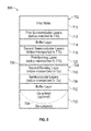
FIG. 9 is an exemplary process flow diagram illustrating a method of fabricating the semiconductor device shown inFIG. 8 . - As shown in
FIG. 1 , apreassembled structure 100 according to an embodiment of the disclosure may include afirst subassembly 102 and asecond subassembly 104. Thefirst subassembly 102 may include afirst wafer 110 and afirst bonding layer 120 directly adjacent and upon afirst surface 110a of thefirst wafer 110. Thefirst wafer 110 may be a semiconductor selected from group III-V materials. In an embodiment, thefirst wafer 110 may be selected from the group consisting of silicon (Si), germanium (Ge), GaAs-based, InP-based, GaP based, GaSb-based, Ga(In)N-based materials. Thefirst surface 110a of thefirst wafer 110 may be a surface of a material layer selected from the group consisting of silicon (Si), germanium (Ge), Gallium Arsenide (GaAs), Indium Phosphide (InP), Gallium Phosphide (GaP), Gallium Antimonide (GaSb), Gallium Indium Arsenide (GaInAs), Gallium Indium Phosphide (GaInP), Gallium Indium Nitride Ga(In)N materials. - The
first bonding layer 120 may be epitaxially grown upon thefirst surface 110a of thefirst wafer 110. In one embodiment, thefirst bonding layer 120 may be an (Al)(Ga)InP(As)(Sb) material having a relatively high dopant concentration equal to or greater than about 5 x 10¹⁸/cm3. It is to be understood that a relatively high doping concentration may not be necessary for sufficient mechanical bonding, but may be needed for achieving a low electrical resistance across a bonded interface (shown inFIG. 2 as a bonded interface 150). However, if a low electrical resistance across the bondedinterface 150 is not required, then a relatively high doping concentration in thefirst bonding layer 120 may not be necessary. As used herein, and as conventional in the art, the use of parentheses in the (Al)(Ga)InP(As)(Sb) material indicates that the incorporation of aluminum, gallium, arsenic, and antimony is optional. In the embodiment as shown inFIG. 1 , thefirst bonding layer 120 may be lattice-matched to thefirst wafer 110, and may include afirst bonding surface 120a. - The
second subassembly 104 may include asecond wafer 130, an optional buffer layer, and asecond bonding layer 140. In the embodiment as shown inFIG. 1 , thesecond bonding layer 140 may be directly adjacent and upon asecond surface 130a of thesecond wafer 130. In one non-limiting embodiment, thesecond wafer 130 may be a Ge substrate wafer. However, it is to be understood that thesecond wafer 130 may be constructed of other materials as well such as, for example, GaAs. Thesecond wafer 130 may be used as a growth substrate as well as for structural support. Specifically, thesecond wafer 130 may be used as a substrate for epitaxial growth of thesecond bonding layer 140 as well as the main mechanical support for an assembled semiconductor device 200 (shown inFIG. 2 ). - In one embodiment, the
second wafer 130 may include anactive Ge subcell 134. However, it is to be understood that in some embodiments, the Ge subcell 134 may be omitted. In one exemplary embodiment, the Ge subcell 134 may include an energy bandgap of about 0.67 eV. The Ge subcell 134 may be created by a diffusion of dopants into a surface layer of thesecond wafer 130. In other words, the Ge subcell 134 may not be epitaxially grown. Thus, the Ge subcell may be part of thesecond wafer 130. - The
second bonding layer 140 may be epitaxially grown upon thesecond surface 130a of thesecond wafer 130. Similar to thefirst bonding layer 120, in one embodiment thesecond bonding layer 140 may also be an (Al)(Ga)InP(As)(Sb) material having a relatively high dopant concentration equal to or greater than about 5x10¹⁸/cm3. It is to be understood that a relatively high doping concentration may not be necessary for sufficient mechanical bonding, but may be needed for achieving a low electrical resistance across the bonded interface (shown inFIG. 2 as the bonded interface 150). However, if a low electrical resistance across the bonded interface is not required, then a relatively high doping concentration in thesecond bonding layer 140 may not be necessary. - In the exemplary embodiment as shown in
FIG. 1 , thesecond bonding layer 140 may be lattice-matched to thesecond wafer 130 of thesecond subassembly 104. However, it is to be understood that in other embodiments thesecond bonding layer 140 may also be lattice-mismatched to thesecond wafer 130 as well, and are described in detail below and illustrated inFIGS. 4-9 . Thesecond bonding layer 140 of thesecond subassembly 104 may be lattice-mismatched to thefirst bonding layer 120 of thefirst subassembly 102. In all the embodiments as described and shown inFIGS. 1-9 , thefirst bonding layer 120 and thesecond bonding layer 140 may be lattice-mismatched to one another. -
FIG. 2 is an illustration of thesemiconductor device 200 according to an embodiment of the disclosure, where thefirst bonding layer 120 and thesecond bonding layer 140 have been bonded together to join thefirst subassembly 102 to thesecond subassembly 104. In one embodiment, thesemiconductor device 200 may be a photovoltaic device, a solar cell, a light sensor, light emitting diode, or a transistor. - The
first subassembly 102 and thesecond subassembly 104 may be directly bonded to one another by placing thefirst bonding layer 120 and thesecond bonding layer 140 in direct contact with one another, where heat and pressure may be applied to bond thefirst subassembly 102 and thesecond subassembly 104 together. Referring toFIGS. 1-2 , thefirst bonding surface 120a and asecond bonding surface 140a may be placed in contact with one another, and diffuse together to form the bondedinterface 150. In one embodiment, thefirst bonding surface 120a and thesecond bonding surface 140a may be polished prior to bringing thefirst bonding layer 120 and thesecond bonding layer 140 into contact. In one embodiment, the polishing may be performed by Chemical Mechanical Polishing (CMP), with bonding performed using conventional wafer bonding equipment. - Once the
first bonding surface 120a and the second bonding surface 140b have been placed into contact with one another, thefirst subassembly 102 and thesecond subassembly 104 may be heated to a bonding temperature of between about 300°C to about 500°C. Thesemiconductor device 200 may be heated at a pressure of between about 20 psi and about 50 psi. Thesemiconductor device 200 may be heated under pressure for about 20 to 300 minutes. Direct semiconductor bonding with (Al)GaInP(As)(Sb) bonding layers has achieved bond strength greater than 4.1 J/m2, electrical resistance as low as 0.3 Ohm-cm2 and optical transparency of greater than 97% across a bonded interface (e.g., the bondedinterface 150 as shown inFIG. 2 ). After direct bonding, thefirst wafer 110 may be removed. -
FIG. 3 illustrates an exemplary process flow diagram of amethod 300 for creating thesemiconductor device 200 as shown inFIG. 2 . Referring generally toFIGS. 1-3 ,method 300 may begin atblock 302, where thefirst bonding layer 120 may be epitaxially grown upon thefirst surface 110a of thefirst wafer 110 of thefirst subassembly 102. As discussed above, thefirst bonding layer 120 may be lattice-matched to thefirst wafer 110.Method 300 may then proceed to block 304. - In
block 304, thesecond bonding layer 140 may be epitaxially grown upon thesecond surface 130a of thesecond wafer 130 of thesecond subassembly 104. As discussed above, thesecond bonding layer 140 may be lattice-matched to thesecond wafer 130. However thesecond bonding layer 140 of thesecond subassembly 104 may be lattice-mismatched to thefirst bonding layer 120 of thefirst subassembly 102.Method 300 may then proceed to block 306.
Inblock 306, thefirst subassembly 102 and thesecond subassembly 104 may be directly bonded to one another at thefirst bonding surface 120a and thesecond bonding surface 140a, thus creating the semiconductor device 200 (shown inFIG. 2 ). Specifically, thefirst bonding surface 120a and thesecond bonding surface 140a (FIG. 1 ) may be placed in contact with one another, and heated to the bonding temperature. Thefirst bonding layer 120 and the second bonding layers 140 diffuse together to form the bonded interface 150 (seen inFIG. 2 ).Method 300 may then terminate. -
FIG. 4 illustrates an alternative embodiment ofpreassembled structure 400 according to an embodiment of the disclosure. Thepreassembled structure 400 may include afirst subassembly 402 and asecond subassembly 404. Thefirst subassembly 402 may include afirst wafer 410, semiconductor layers 412, and afirst bonding layer 420. The semiconductor layers 412 may be directly adjacent and upon afirst surface 410a of thefirst wafer 410. In one embodiment, the semiconductor layers 412 may be a photovoltaic device, or a solar cell having one or more subcells. Thefirst bonding layer 420 may be directly adjacent and upon asemiconductor surface 412a of the semiconductor layers 412. Similar to the embodiment as described above and shown inFIGS. 1-3 , thefirst wafer 410 may be a semiconductor selected from group III-V materials. In an embodiment, thefirst wafer 410 may be selected from the group consisting of silicon (Si), germanium (Ge), Gallium Arsenide (GaAs), Indium Phosphide (InP), Gallium Phosphide (GaP), Gallium Antimonide (GaSb), Gallium Indium Arsenide (GaInAs), Gallium Indium Phosphide (GaInP), Gallium Indium Nitride Ga(In)N materials. - The semiconductor layers 412 may be epitaxially grown upon the
first surface 410a of thefirst wafer 410. The semiconductor layers 412 may be lattice-matched to thefirst wafer 410. Thefirst bonding layer 420 may be epitaxially grown upon thesemiconductor surface 412a of the semiconductor layers 412. Similar to the embodiment as shown inFIGS. 1-3 and described above, thefirst bonding layer 420 may be an (Al)(Ga)InP(As)(Sb) material, and in one embodiment may have a relatively high dopant concentration equal to or greater than about 5 x 10¹⁸/cm3. Thefirst bonding layer 420 may also be lattice-matched to thefirst wafer 410, and may include afirst bonding surface 420a. - The
second subassembly 404 may include asecond wafer 430, abuffer layer 432, semiconductor layers 436, and asecond bonding layer 440. In the embodiment as shown inFIG. 4 , thebuffer layer 432 may be directly adjacent and upon asecond surface 430a of thesecond wafer 430. The semiconductor layers 436 may be directly adjacent and upon abuffer surface 432a of thebuffer layer 432. Thesecond bonding layer 440 may be directly adjacent and upon asemiconductor surface 436a of the semiconductor layers 436. - Similar to the embodiment as described above and shown in
FIGS. 1-3 , thesecond wafer 430 may be a Ge substrate, and may be used as a growth substrate as well as for structural support. Specifically, thesecond wafer 430 may be used as a substrate for epitaxial growth of thebuffer layer 432 as well the main mechanical support for an assembled semiconductor device 500 (shown inFIG. 5 ). Thebuffer layer 432 may be epitaxially grown upon thesecond surface 430a of thesecond wafer 430. In one embodiment, thesecond wafer 430 may include anactive Ge subcell 434. However, it is to be understood that in some embodiments, the Ge subcell 434 may be omitted. - In the embodiment as shown in
FIG. 4 , thebuffer layer 432 may be epitaxially grown upon thesecond surface 430a of thesecond wafer 430. Thebuffer layer 432 may be a metamorphic transparent graded buffer. In the embodiments as described, the term transparent may be defined as a transmission of equal to or greater than about ninety-seven percent of the light or electromagnetic radiation of a wavelength for activating a cell or subcell disposed underneath. Thebuffer layer 432 may be used to epitaxially grow material that is lattice-mismatched to thesecond wafer 430. For example, in the embodiment as shown inFIG. 4 thebuffer layer 432 may be used to grow the semiconductor layers 436. The semiconductor layers 436 may be lattice-mismatched to thesecond wafer 430. Thebuffer layer 432 may absorb the strain of lattice-mismatch, and generally prevents the vertical propagation of dislocations. - The
second bonding layer 440 may be epitaxially grown upon thesemiconductor surface 436a of the semiconductor layers 436. Thesecond bonding layer 440 may include asecond bonding surface 440a. Similar to thefirst bonding layer 420, thesecond bonding layer 440 may be an (Al)(Ga)InP(As)(Sb) material, and may have a relatively high dopant concentration equal to or greater than about 5 x 10¹⁸/cm3. In the embodiment as shown inFIG. 4 , both the semiconductor layers 436 and thesecond bonding layer 440 of thesecond subassembly 404 may be lattice-mismatched to thesecond wafer 430. Thesecond bonding layer 440 may be lattice-matched to the semiconductor layers 436. Moreover, thefirst bonding layer 420 of thefirst subassembly 402 may be lattice-mismatched to thesecond bonding layer 440 of thesecond subassembly 404. -
FIG. 5 is an illustration of thesemiconductor device 500 according to an embodiment of the disclosure, where thefirst bonding layer 420 and thesecond bonding layer 440 have been bonded together to join thefirst subassembly 402 to thesecond subassembly 404. Similar to the embodiment as shown inFIG. 2 , thefirst subassembly 402 and thesecond subassembly 404 may be directly bonded to one another by placing thefirst bonding layer 420 and thesecond bonding layer 440 in direct contact with one another, where heat and pressure may be applied to bond thefirst subassembly 402 and thesecond subassembly 404 together. Referring toFIGS. 4-5 , thefirst bonding surface 420a and thesecond bonding surface 440a may be placed in contact with one another, and diffuse together to form the bondedinterface 450. -
FIG. 6 illustrates an exemplary process flow diagram of amethod 600 for creating thesemiconductor device 500 as shown inFIG. 5 . Referring generally toFIGS. 4-6 , themethod 600 may begin atblock 602, where the semiconductor layers 412 and thefirst bonding layer 420 may be epitaxially grown upon thefirst wafer 410 of thefirst subassembly 402. Specifically, the semiconductor layers 412 may be grown upon thefirst surface 410a of thefirst wafer 410, and thefirst bonding layer 420 may be epitaxially grown upon thesemiconductor surface 412a of the semiconductor layers 412.Method 600 may then proceed to block 604. - In
block 604, thebuffer layer 432 may be epitaxially grown upon thesecond surface 430a of thesecond wafer 430 of thesecond subassembly 404.Method 600 may then proceed to block 606. - In
block 606, the semiconductor layers 436 may be epitaxially grown upon thebuffer surface 432a of thebuffer layer 432 of thesecond subassembly 404. As described above, the semiconductor layers 436 may be lattice-mismatched to thesecond wafer 430.Method 600 may then proceed to block 608. - In
block 608, thesecond bonding layer 440 may be epitaxially grown upon thesemiconductor surface 436a of the semiconductor layers 436 of thesecond subassembly 404. As discussed above, thesecond bonding layer 440 may be lattice-mismatched to thesecond wafer 430. Thesecond bonding layer 440 may also be lattice-mismatched to thefirst bonding layer 420 of thefirst subassembly 402.Method 600 may then proceed to block 610. - In
block 610, thefirst subassembly 402 and thesecond subassembly 404 may be directly bonded to one another at thefirst bonding surface 420a and thesecond bonding surface 440a, thus creating the semiconductor device 500 (shown inFIG. 5 ). Specifically, thefirst bonding surface 420a and thesecond bonding surface 440a (FIG. 4 ) may be placed in contact with one another, and heated to the bonding temperature. Thefirst bonding layer 420 and thesecond bonding layer 440 diffuse together to form the bonded interface 450 (seen inFIG. 5 ).Method 600 may then terminate. -
FIG. 7 illustrates an alternative embodiment ofpreassembled structure 700 according to an embodiment of the disclosure. Thepreassembled structure 700 may include afirst subassembly 702 and asecond subassembly 704. Thefirst subassembly 702 may include afirst wafer 710, first semiconductor layers 712, abuffer layer 714, second semiconductor layers 716, and afirst bonding layer 720. The first semiconductor layers 712 may be directly adjacent and upon afirst surface 710a of thefirst wafer 710. In one embodiment, the first semiconductor layers 712 may be a photovoltaic device, or a solar cell having one or more subcells. Thebuffer layer 714 may be epitaxially grown upon afirst semiconductor surface 712a of the first semiconductor layers 712. Similar to thebuffer layer 432 of thesecond subassembly 404 shown inFIGS. 4-5 , thebuffer layer 714 may also be a metamorphic transparent graded buffer. The second semiconductor layers 716 may be directly adjacent and upon abuffer surface 714a of thebuffer layer 714. The second semiconductor layers 716 may also be a photovoltaic device, or a solar cell having one or more subcells. Thefirst bonding layer 720 may be directly adjacent and upon asecond semiconductor surface 716a of the second semiconductor layers 716. - Similar to the embodiments as described above and shown in
FIGS. 1-6 , thefirst wafer 710 may be a semiconductor selected from group III-V materials. In an embodiment, thefirst wafer 710 may be selected from the group consisting of silicon (Si), germanium (Ge), Gallium Arsenide (GaAs), Indium Phosphide (InP), Gallium Phosphide (GaP), Gallium Antimonide (GaSb), , Gallium Indium Arsenide (GaInAs), Gallium Indium Phosphide (GaInP), Gallium Indium Nitride Ga(In)N materials. The first semiconductor layers 712 may be epitaxially grown upon thefirst surface 710a of thefirst wafer 710, and may be lattice-matched to thefirst wafer 710. - The
buffer layer 714 may be epitaxially grown upon thefirst semiconductor surface 712a of thefirst semiconductor layer 712. Thebuffer layer 714 may be used to epitaxially grow material that is lattice-mismatched to thefirst wafer 710. For example, in the embodiment as shown inFIG. 7 thebuffer layer 714 may be used to grow the second semiconductor layers 716, which may be lattice-mismatched to thefirst wafer 710. - The
first bonding layer 720 may be epitaxially grown upon thesecond semiconductor surface 716a of the second semiconductor layers 716. Similar to the embodiment as shown inFIGS. 1-6 and described above, thefirst bonding layer 720 may be an (Al)(Ga)InP(As)(Sb) material, and in one embodiment may have a relatively high dopant concentration equal to or greater than about 5 x 10¹⁸g/cm3. In the embodiment as shown inFIG. 7 , thefirst bonding layer 720 may be lattice-mismatched to thefirst wafer 710 and lattice-matched to the second semiconductor layers 716, and may include afirst bonding surface 720a. - The
second subassembly 704 may include asecond wafer 730, abuffer layer 732, semiconductor layers 736, and asecond bonding layer 740. In the embodiment as shown inFIG. 7 , thebuffer layer 732 may be directly adjacent and upon asecond surface 730a of thesecond wafer 730. The semiconductor layers 736 may be directly adjacent and upon abuffer surface 732a of thebuffer layer 732. Thesecond bonding layer 740 may be directly adjacent and upon asemiconductor surface 736a of the semiconductor layers 736. - Similar to the embodiment as described above and shown in
FIGS. 1-6 , thesecond wafer 730 may be a Ge substrate, and may be used as a growth substrate as well as for structural support. Specifically, thesecond wafer 730 may be used as a substrate for epitaxial growth of thebuffer layer 732, as well as the main mechanical support for an assembled semiconductor device 800 (shown inFIG. 8 ). Thebuffer layer 732 may be epitaxially grown upon thesecond surface 730a of thesecond wafer 730. In one embodiment, thesecond wafer 730 may include anactive Ge subcell 734. However, it is to be understood that in some embodiments, the Ge subcell 734 may be omitted. - The
buffer layer 732 may be epitaxially grown upon thesecond surface 730a of thesecond wafer 730. Thebuffer layer 732 may be a metamorphic transparent graded buffer. Thebuffer layer 732 may be used to epitaxially grow material that is lattice-mismatched to thesecond wafer 730. For example, in the embodiment as shown inFIG. 7 , thebuffer layer 732 may be used to grow the semiconductor layers 736, which may be lattice-mismatched to thesecond wafer 730. Specifically, the semiconductor layers 736 may be epitaxially grown upon thebuffer surface 732a of thebuffer layer 732. - The
second bonding layer 740 may be epitaxially grown upon thesemiconductor surface 736a of the semiconductor layers 736. Thesecond bonding layer 740 may include asecond bonding surface 740a. Similar to thefirst bonding layer 720 of thefirst subassembly 702, thesecond bonding layer 440 may be an (Al)(Ga)InP(As)(Sb) material, and may have a relatively high dopant concentration equal to or greater than about 5 x 10¹⁸/cm3. In the embodiment as shown inFIG. 7 , both the semiconductor layers 736 and thesecond bonding layer 740 of thesecond subassembly 704 may be lattice-mismatched to thesecond wafer 730. The semiconductor layers 736 and thesecond bonding layer 740 may be lattice-matched to each other. Moreover, thefirst bonding layer 720 of thefirst subassembly 702 may be lattice-mismatched to thesecond bonding layer 740 of thesecond subassembly 704. -
FIG. 8 is an illustration of thesemiconductor device 800 according to an embodiment of the disclosure, where thefirst bonding layer 720 and thesecond bonding layer 740 have been bonded together to join thefirst subassembly 702 to thesecond subassembly 704. Similar to the embodiment as shown inFIGS. 2 and5 , thefirst subassembly 702 and thesecond subassembly 704 may be directly bonded to one another by placing thefirst bonding layer 720 and thesecond bonding layer 740 in direct contact with one another, where heat and pressure may be applied to bond thefirst subassembly 702 and thesecond subassembly 704 together. Referring toFIGS. 7-8 , thefirst bonding surface 720a and thesecond bonding surface 740a may be placed in contact with one another, and diffuse together to form a bondedinterface 750. -
FIG. 9 illustrates an exemplary process flow diagram of amethod 900 for creating thesemiconductor device 800 as shown inFIG. 8 . Referring generally toFIGS. 7-9 , themethod 900 may begin atblock 902, where the first semiconductor layers 712 may be epitaxially grown upon thefirst wafer 710 of thefirst subassembly 702. As described above, the first semiconductor layers 712 may be lattice-matched to thefirst wafer 710.Method 900 may then proceed to block 904. - In
block 904, thebuffer layer 714 may be epitaxially grown upon thefirst semiconductor surface 712a of the first semiconductor layers 712 of thefirst subassembly 702.Method 900 may then proceed to block 906. - In
block 906, the second semiconductor layers 716 may be epitaxially grown upon thebuffer surface 714a of thebuffer layer 714 of thefirst subassembly 702. As described above, the second semiconductor layers 716 may be lattice-mismatched to thefirst wafer 710.Method 900 may then proceed to block 908. - In
block 908, thefirst bonding layer 720 may be epitaxially grown upon thesecond semiconductor surface 716a of the second semiconductor layers 716 of thefirst subassembly 702. As described above, thefirst bonding layer 720 may be lattice-mismatched to thefirst wafer 710, but may be lattice-matched to the second semiconductor layers 716.Method 900 may then proceed to block 910. - In
block 910, thebuffer layer 732 may be epitaxially grown upon thesecond surface 730a of thesecond wafer 730 of thesecond subassembly 704.Method 900 may then proceed to block 912. - In
block 912, the semiconductor layers 736 may be epitaxially grown upon thebuffer surface 732a of thebuffer layer 732 of thesecond subassembly 704. As described above, the semiconductor layers 736 may be lattice-mismatched to thesecond wafer 730.Method 900 may then proceed to block 914. - In
block 914, thesecond bonding layer 740 may be epitaxially grown upon thesemiconductor surface 736a of the semiconductor layers 736 of thesecond subassembly 704. As discussed above, thesecond bonding layer 740 may be lattice-mismatched to thesecond wafer 730, as well as thefirst bonding layer 720 of thefirst subassembly 702. Thesecond bonding layer 740 may also be lattice-matched to the semiconductor layers 736.Method 900 may then proceed to block 916. - In
block 916, thefirst subassembly 702 and thesecond subassembly 704 may be directly bonded to one another at thefirst bonding surface 720a and thesecond bonding surface 740a, thus creating the semiconductor device 800 (shown inFIG. 8 ). Specifically, thefirst bonding surface 720a and thesecond bonding surface 740a (FIG. 7 ) may be placed in contact with one another, and heated to the bonding temperature. Thefirst bonding layer 720 and thesecond bonding layer 740 diffuse together to form the bonded interface 750 (seen inFIG. 8 ).Method 900 may then terminate. - Referring generally to
FIGS. 1-9 , the disclosed semiconductor devices as described above may include a wider range of bandgap combinations between the various device components when compared to some other types of semiconductor devices currently available that only include directly bonded lattice-matched device components. This is because all the disclosed semiconductor devices as described above each include directly bonded lattice-mismatched device components. Lattice-mismatching various device components may widen the possible range of bandgap combinations and may also enhance material quality of the semiconductor device. It should be noted that direct bonding of metamorphic components is typically not practiced in industry at this time. - Additionally, the disclosed semiconductor devices each include the Ge substrate, and may include the active Ge subcell. The Ge subcell may be used to replace an epitaxially-grown GaInAs subcell including an energy bandgap of about 0.7 eV, which is typically found in a semiconductor device that is grown using inverted metamorphic (IMM) technologies. The Ge subcell may have equal or better performance retention after radiation when compared to the GaInAs subcell found in semiconductor devices grown using IMM technologies. Replacing the GaInAs subcell with the active Ge subcell may substantially reduce the overall cost of the semiconductor device. Moreover, semiconductor devices grown using IMM technologies may also require an additional device handle as well. In contrast, the disclosed Ge substrate may be used as the main mechanical support for the semiconductor device. Thus, no additional device handle may be needed. The disclosed Ge substrate may provide other benefits during semiconductor fabrication as well such as, for example, spalling compatibility, etching chemical selectivity, and simplicity in back-side metal contacts having substrate polarity. The Ge substrate may be relatively thin (e.g., having a thickness of about fifty microns), which may also reduce the overall mass of the disclosed semiconductor devices. Also, the Ge substrate may provide an enhanced power density.
- For example, in one embodiment the disclosed semiconductor device may be a directly bonded five-junction solar cell grown on a Ge substrate including an active Ge subcell. Specifically, the solar cell may be comprised of a first subassembly including lattice-matched device components with relatively high energy bandgaps (e.g., ranging from about 1.3 eV to about 2.0 eV). The first subassembly may be directly bonded to a second subassembly. The second subassembly may include the Ge substrate, a single buffer layer, and a device component grown upon the buffer layer and lattice-mismatched to the Ge substrate. The active Ge subcell of the Ge substrate and the device component of the second subassembly may include relatively low energy bandgaps (e.g., 0.67 eV for the Ge subcell and 1.0-1.1 eV for the device component). Some types of solar cells currently available that are grown using IMM technologies may include multiple buffer layers to absorb the strain of lattice-mismatch between various device components. In contrast, the exemplary solar cell as described only includes one buffer layer, which may reduce the overall cost.
- While the forms of apparatus and methods herein described constitute preferred embodiments of this invention, it is to be understood that the invention is not limited to these precise forms of apparatus and methods, and the changes may be made therein without departing from the scope of the invention.
Claims (15)
- A semiconductor device, comprising:a first subassembly comprising a first bonding layer and a first substrate; anda second subassembly, comprising:a second substrate; anda second bonding layer directly bonded to the first bonding layer, wherein the first bonding layer and the second bonding layer are lattice-mismatched to one another, and wherein at least one of the following is selected:the first bonding layer is lattice-mismatched to the first substrate, and the second bonding layer is lattice-mismatched to the second substrate.
- The semiconductor device of claim 1, wherein a buffer layer is epitaxially grown on the second substrate.
- The semiconductor device of claim 1 or claim 2, wherein the second substrate is constructed of germanium (Ge) and optionally
wherein the second substrate includes an active Ge subcell. - The semiconductor device of any preceding claim, wherein the second subassembly includes semiconductor layers lattice-mismatched to the second substrate.
- The semiconductor device of any preceding claim, wherein the first subassembly includes first semiconductor layers lattice-matched to the first substrate.
- The semiconductor device of claim 5, wherein the first subassembly includes a buffer layer epitaxially grown on the first semiconductor layers.
- The semiconductor device of claim 6, wherein the first subassembly includes second semiconductor layers lattice-mismatched to the first substrate.
- The semiconductor device of claim 5, wherein the second semiconductor layers are epitaxially grown on the buffer layer.
- The semiconductor device of any preceding claim, wherein at least one of the first subassembly and the second subassembly includes one of a photovoltaic device and a solar cell.
- A method of making a semiconductor device, comprising;
providing a first subassembly comprising a first bonding layer and a first substrate;
providing a second subassembly comprising a second substrate and a second bonding layer;
directly bonding the first bonding layer and the second bonding layer together, wherein the first bonding layer and the second bonding layer are lattice-mismatched to one another; and
selecting at least one of the following:lattice-mismatching the first bonding layer to the first substrate, and lattice-mismatching the second bonding layer to the second substrate. - The method of claim 10, comprising selecting lattice-mismatching the second bonding layer to the second substrate, and epitaxially growing a buffer layer on the second substrate.
- The method of claim 10 or claim 11, comprising constructing the second substrate of germanium (Ge) and optionally creating an active Ge subcell within the second substrate by a diffusion of dopants into a layer of the second substrate.
- The method of any one of claims 10 to 12, comprising epitaxially growing first semiconductor layers upon the first substrate of the first subassembly, wherein the first semiconductor layers are lattice-matched to the first substrate.
- The method of any one of claims 10 to 13, comprising epitaxially growing a buffer layer upon the first semiconductor layers.
- The method of claim 11, comprising epitaxially growing second semiconductor layers on the buffer layer, wherein the second semiconductor layers are lattice-mismatched to the first substrate, and wherein the first bonding layer is lattice-mismatched to the first substrate.
Applications Claiming Priority (1)
| Application Number | Priority Date | Filing Date | Title |
|---|---|---|---|
| US14/152,464 US9331227B2 (en) | 2014-01-10 | 2014-01-10 | Directly bonded, lattice-mismatched semiconductor device |
Publications (2)
| Publication Number | Publication Date |
|---|---|
| EP2894661A1 true EP2894661A1 (en) | 2015-07-15 |
| EP2894661B1 EP2894661B1 (en) | 2022-09-07 |
Family
ID=52278534
Family Applications (1)
| Application Number | Title | Priority Date | Filing Date |
|---|---|---|---|
| EP15150677.1A Active EP2894661B1 (en) | 2014-01-10 | 2015-01-09 | Directly bonded, lattice-mismatched semiconductor device |
Country Status (4)
| Country | Link |
|---|---|
| US (1) | US9331227B2 (en) |
| EP (1) | EP2894661B1 (en) |
| JP (1) | JP6434313B2 (en) |
| CN (1) | CN104779211B (en) |
Families Citing this family (4)
| Publication number | Priority date | Publication date | Assignee | Title |
|---|---|---|---|---|
| FR3047351B1 (en) | 2016-02-03 | 2023-07-14 | Soitec Silicon On Insulator | ADVANCED SUBSTRATE |
| AU2017391778B2 (en) * | 2017-01-04 | 2022-09-29 | Shih-Hsien Tseng | Pixel unit structure and manufacturing method thereof |
| KR20190044235A (en) | 2017-10-20 | 2019-04-30 | 한국전력공사 | Multi junction solar cell having lattice mismatched buffer structure and Method for manufacturing the same |
| CN111653649B (en) * | 2020-06-05 | 2023-09-05 | 中国科学院上海微系统与信息技术研究所 | Preparation method of Si-based InGaAs photoelectric detector and photoelectric detector |
Citations (4)
| Publication number | Priority date | Publication date | Assignee | Title |
|---|---|---|---|---|
| US20020052061A1 (en) * | 2000-08-04 | 2002-05-02 | Fitzgerald Eugene A. | Silicon wafer with embedded optoelectronic material for monolithic OEIC |
| US20030213950A1 (en) * | 2000-05-31 | 2003-11-20 | Applied Optoelectronics, Inc. | Alternative substrates for epitaxial growth |
| US20050067377A1 (en) * | 2003-09-25 | 2005-03-31 | Ryan Lei | Germanium-on-insulator fabrication utilizing wafer bonding |
| US20120138116A1 (en) * | 2010-12-03 | 2012-06-07 | The Boeing Company | Direct wafer bonding |
Family Cites Families (11)
| Publication number | Priority date | Publication date | Assignee | Title |
|---|---|---|---|---|
| JP2705283B2 (en) * | 1990-06-14 | 1998-01-28 | 日立電線株式会社 | Stacked solar cell and method of manufacturing the same |
| US7157119B2 (en) * | 2002-06-25 | 2007-01-02 | Ppg Industries Ohio, Inc. | Method and compositions for applying multiple overlying organic pigmented decorations on ceramic substrates |
| US6951819B2 (en) * | 2002-12-05 | 2005-10-04 | Blue Photonics, Inc. | High efficiency, monolithic multijunction solar cells containing lattice-mismatched materials and methods of forming same |
| JP2005159071A (en) * | 2003-11-27 | 2005-06-16 | Ricoh Co Ltd | Semiconductor device, manufacturing method thereof, and optical transmission system |
| US8227689B2 (en) * | 2004-06-15 | 2012-07-24 | The Boeing Company | Solar cells having a transparent composition-graded buffer layer |
| US10374120B2 (en) * | 2005-02-18 | 2019-08-06 | Koninklijke Philips N.V. | High efficiency solar cells utilizing wafer bonding and layer transfer to integrate non-lattice matched materials |
| US11211510B2 (en) * | 2005-12-13 | 2021-12-28 | The Boeing Company | Multijunction solar cell with bonded transparent conductive interlayer |
| US8236600B2 (en) * | 2008-11-10 | 2012-08-07 | Emcore Solar Power, Inc. | Joining method for preparing an inverted metamorphic multijunction solar cell |
| US20110132445A1 (en) * | 2009-05-29 | 2011-06-09 | Pitera Arthur J | High-efficiency multi-junction solar cell structures |
| US10170652B2 (en) * | 2011-03-22 | 2019-01-01 | The Boeing Company | Metamorphic solar cell having improved current generation |
| US20140137930A1 (en) * | 2012-11-16 | 2014-05-22 | Solar Junction Corporation | Multijunction solar cells |
-
2014
- 2014-01-10 US US14/152,464 patent/US9331227B2/en active Active
- 2014-12-08 CN CN201410741083.XA patent/CN104779211B/en active Active
-
2015
- 2015-01-06 JP JP2015000770A patent/JP6434313B2/en active Active
- 2015-01-09 EP EP15150677.1A patent/EP2894661B1/en active Active
Patent Citations (4)
| Publication number | Priority date | Publication date | Assignee | Title |
|---|---|---|---|---|
| US20030213950A1 (en) * | 2000-05-31 | 2003-11-20 | Applied Optoelectronics, Inc. | Alternative substrates for epitaxial growth |
| US20020052061A1 (en) * | 2000-08-04 | 2002-05-02 | Fitzgerald Eugene A. | Silicon wafer with embedded optoelectronic material for monolithic OEIC |
| US20050067377A1 (en) * | 2003-09-25 | 2005-03-31 | Ryan Lei | Germanium-on-insulator fabrication utilizing wafer bonding |
| US20120138116A1 (en) * | 2010-12-03 | 2012-06-07 | The Boeing Company | Direct wafer bonding |
Also Published As
| Publication number | Publication date |
|---|---|
| CN104779211A (en) | 2015-07-15 |
| JP2015156478A (en) | 2015-08-27 |
| US9331227B2 (en) | 2016-05-03 |
| US20150200321A1 (en) | 2015-07-16 |
| CN104779211B (en) | 2018-12-28 |
| JP6434313B2 (en) | 2018-12-05 |
| EP2894661B1 (en) | 2022-09-07 |
Similar Documents
| Publication | Publication Date | Title |
|---|---|---|
| KR101719857B1 (en) | Direct wafer bonding | |
| TWI681565B (en) | Non-destructive wafer recycling for epitaxial lift-off thin-film device using a superlattice epitaxial layer | |
| US8410523B2 (en) | Misfit dislocation forming interfacial self-assembly for growth of highly-mismatched III-SB alloys | |
| KR101719620B1 (en) | Manufacture of multijunction solar cell devices | |
| US20150053257A1 (en) | Multi-junction solar cell and use thereof | |
| US20110048517A1 (en) | Multijunction Photovoltaic Cell Fabrication | |
| TW201436266A (en) | Multi-junction solar cell | |
| EP2894661A1 (en) | Directly bonded, lattice-mismatched semiconductor device | |
| JP2015512150A (en) | Thermal surface treatment for wafer reuse after epitaxial lift-off | |
| US9425104B2 (en) | Complementary metal oxide semiconductor device and method of manufacturing the same | |
| CN107910750B (en) | A kind of preparation method of semiconductor laser material | |
| KR101700728B1 (en) | Manufacture of multijunction solar cell devices | |
| KR101700724B1 (en) | Manufacture of multijunction solar cell devices | |
| US8853529B2 (en) | Flexible III-V solar cell structure | |
| KR101370611B1 (en) | Solar cell of multi junction structure | |
| KR102203033B1 (en) | Planar heterogeneous device | |
| Onno et al. | 1.7 eV Al0. 2Ga0. 8As solar cells epitaxially grown on silicon by SSMBE using a superlattice and dislocation filters | |
| US20140057385A1 (en) | Iii-v photovoltaic element and fabrication method |
Legal Events
| Date | Code | Title | Description |
|---|---|---|---|
| PUAI | Public reference made under article 153(3) epc to a published international application that has entered the european phase |
Free format text: ORIGINAL CODE: 0009012 |
|
| 17P | Request for examination filed |
Effective date: 20150109 |
|
| AK | Designated contracting states |
Kind code of ref document: A1 Designated state(s): AL AT BE BG CH CY CZ DE DK EE ES FI FR GB GR HR HU IE IS IT LI LT LU LV MC MK MT NL NO PL PT RO RS SE SI SK SM TR |
|
| AX | Request for extension of the european patent |
Extension state: BA ME |
|
| STAA | Information on the status of an ep patent application or granted ep patent |
Free format text: STATUS: EXAMINATION IS IN PROGRESS |
|
| 17Q | First examination report despatched |
Effective date: 20201119 |
|
| GRAP | Despatch of communication of intention to grant a patent |
Free format text: ORIGINAL CODE: EPIDOSNIGR1 |
|
| STAA | Information on the status of an ep patent application or granted ep patent |
Free format text: STATUS: GRANT OF PATENT IS INTENDED |
|
| INTG | Intention to grant announced |
Effective date: 20220411 |
|
| GRAS | Grant fee paid |
Free format text: ORIGINAL CODE: EPIDOSNIGR3 |
|
| GRAA | (expected) grant |
Free format text: ORIGINAL CODE: 0009210 |
|
| STAA | Information on the status of an ep patent application or granted ep patent |
Free format text: STATUS: THE PATENT HAS BEEN GRANTED |
|
| AK | Designated contracting states |
Kind code of ref document: B1 Designated state(s): AL AT BE BG CH CY CZ DE DK EE ES FI FR GB GR HR HU IE IS IT LI LT LU LV MC MK MT NL NO PL PT RO RS SE SI SK SM TR |
|
| REG | Reference to a national code |
Ref country code: GB Ref legal event code: FG4D |
|
| REG | Reference to a national code |
Ref country code: CH Ref legal event code: EP Ref country code: AT Ref legal event code: REF Ref document number: 1517760 Country of ref document: AT Kind code of ref document: T Effective date: 20220915 |
|
| REG | Reference to a national code |
Ref country code: IE Ref legal event code: FG4D |
|
| REG | Reference to a national code |
Ref country code: DE Ref legal event code: R096 Ref document number: 602015080658 Country of ref document: DE |
|
| REG | Reference to a national code |
Ref country code: LT Ref legal event code: MG9D |
|
| REG | Reference to a national code |
Ref country code: NL Ref legal event code: MP Effective date: 20220907 |
|
| PG25 | Lapsed in a contracting state [announced via postgrant information from national office to epo] |
Ref country code: SE Free format text: LAPSE BECAUSE OF FAILURE TO SUBMIT A TRANSLATION OF THE DESCRIPTION OR TO PAY THE FEE WITHIN THE PRESCRIBED TIME-LIMIT Effective date: 20220907 Ref country code: RS Free format text: LAPSE BECAUSE OF FAILURE TO SUBMIT A TRANSLATION OF THE DESCRIPTION OR TO PAY THE FEE WITHIN THE PRESCRIBED TIME-LIMIT Effective date: 20220907 Ref country code: NO Free format text: LAPSE BECAUSE OF FAILURE TO SUBMIT A TRANSLATION OF THE DESCRIPTION OR TO PAY THE FEE WITHIN THE PRESCRIBED TIME-LIMIT Effective date: 20221207 Ref country code: LV Free format text: LAPSE BECAUSE OF FAILURE TO SUBMIT A TRANSLATION OF THE DESCRIPTION OR TO PAY THE FEE WITHIN THE PRESCRIBED TIME-LIMIT Effective date: 20220907 Ref country code: LT Free format text: LAPSE BECAUSE OF FAILURE TO SUBMIT A TRANSLATION OF THE DESCRIPTION OR TO PAY THE FEE WITHIN THE PRESCRIBED TIME-LIMIT Effective date: 20220907 Ref country code: FI Free format text: LAPSE BECAUSE OF FAILURE TO SUBMIT A TRANSLATION OF THE DESCRIPTION OR TO PAY THE FEE WITHIN THE PRESCRIBED TIME-LIMIT Effective date: 20220907 Ref country code: ES Free format text: LAPSE BECAUSE OF FAILURE TO SUBMIT A TRANSLATION OF THE DESCRIPTION OR TO PAY THE FEE WITHIN THE PRESCRIBED TIME-LIMIT Effective date: 20220907 |
|
| REG | Reference to a national code |
Ref country code: AT Ref legal event code: MK05 Ref document number: 1517760 Country of ref document: AT Kind code of ref document: T Effective date: 20220907 |
|
| PG25 | Lapsed in a contracting state [announced via postgrant information from national office to epo] |
Ref country code: HR Free format text: LAPSE BECAUSE OF FAILURE TO SUBMIT A TRANSLATION OF THE DESCRIPTION OR TO PAY THE FEE WITHIN THE PRESCRIBED TIME-LIMIT Effective date: 20220907 Ref country code: GR Free format text: LAPSE BECAUSE OF FAILURE TO SUBMIT A TRANSLATION OF THE DESCRIPTION OR TO PAY THE FEE WITHIN THE PRESCRIBED TIME-LIMIT Effective date: 20221208 |
|
| RAP4 | Party data changed (patent owner data changed or rights of a patent transferred) |
Owner name: THE BOEING COMPANY |
|
| PG25 | Lapsed in a contracting state [announced via postgrant information from national office to epo] |
Ref country code: SM Free format text: LAPSE BECAUSE OF FAILURE TO SUBMIT A TRANSLATION OF THE DESCRIPTION OR TO PAY THE FEE WITHIN THE PRESCRIBED TIME-LIMIT Effective date: 20220907 Ref country code: RO Free format text: LAPSE BECAUSE OF FAILURE TO SUBMIT A TRANSLATION OF THE DESCRIPTION OR TO PAY THE FEE WITHIN THE PRESCRIBED TIME-LIMIT Effective date: 20220907 Ref country code: PT Free format text: LAPSE BECAUSE OF FAILURE TO SUBMIT A TRANSLATION OF THE DESCRIPTION OR TO PAY THE FEE WITHIN THE PRESCRIBED TIME-LIMIT Effective date: 20230109 Ref country code: CZ Free format text: LAPSE BECAUSE OF FAILURE TO SUBMIT A TRANSLATION OF THE DESCRIPTION OR TO PAY THE FEE WITHIN THE PRESCRIBED TIME-LIMIT Effective date: 20220907 Ref country code: AT Free format text: LAPSE BECAUSE OF FAILURE TO SUBMIT A TRANSLATION OF THE DESCRIPTION OR TO PAY THE FEE WITHIN THE PRESCRIBED TIME-LIMIT Effective date: 20220907 |
|
| PG25 | Lapsed in a contracting state [announced via postgrant information from national office to epo] |
Ref country code: SK Free format text: LAPSE BECAUSE OF FAILURE TO SUBMIT A TRANSLATION OF THE DESCRIPTION OR TO PAY THE FEE WITHIN THE PRESCRIBED TIME-LIMIT Effective date: 20220907 Ref country code: PL Free format text: LAPSE BECAUSE OF FAILURE TO SUBMIT A TRANSLATION OF THE DESCRIPTION OR TO PAY THE FEE WITHIN THE PRESCRIBED TIME-LIMIT Effective date: 20220907 Ref country code: IS Free format text: LAPSE BECAUSE OF FAILURE TO SUBMIT A TRANSLATION OF THE DESCRIPTION OR TO PAY THE FEE WITHIN THE PRESCRIBED TIME-LIMIT Effective date: 20230107 Ref country code: EE Free format text: LAPSE BECAUSE OF FAILURE TO SUBMIT A TRANSLATION OF THE DESCRIPTION OR TO PAY THE FEE WITHIN THE PRESCRIBED TIME-LIMIT Effective date: 20220907 |
|
| REG | Reference to a national code |
Ref country code: DE Ref legal event code: R097 Ref document number: 602015080658 Country of ref document: DE |
|
| P01 | Opt-out of the competence of the unified patent court (upc) registered |
Effective date: 20230516 |
|
| PG25 | Lapsed in a contracting state [announced via postgrant information from national office to epo] |
Ref country code: NL Free format text: LAPSE BECAUSE OF FAILURE TO SUBMIT A TRANSLATION OF THE DESCRIPTION OR TO PAY THE FEE WITHIN THE PRESCRIBED TIME-LIMIT Effective date: 20220907 Ref country code: AL Free format text: LAPSE BECAUSE OF FAILURE TO SUBMIT A TRANSLATION OF THE DESCRIPTION OR TO PAY THE FEE WITHIN THE PRESCRIBED TIME-LIMIT Effective date: 20220907 |
|
| PLBE | No opposition filed within time limit |
Free format text: ORIGINAL CODE: 0009261 |
|
| STAA | Information on the status of an ep patent application or granted ep patent |
Free format text: STATUS: NO OPPOSITION FILED WITHIN TIME LIMIT |
|
| PG25 | Lapsed in a contracting state [announced via postgrant information from national office to epo] |
Ref country code: DK Free format text: LAPSE BECAUSE OF FAILURE TO SUBMIT A TRANSLATION OF THE DESCRIPTION OR TO PAY THE FEE WITHIN THE PRESCRIBED TIME-LIMIT Effective date: 20220907 |
|
| 26N | No opposition filed |
Effective date: 20230608 |
|
| PG25 | Lapsed in a contracting state [announced via postgrant information from national office to epo] |
Ref country code: SI Free format text: LAPSE BECAUSE OF FAILURE TO SUBMIT A TRANSLATION OF THE DESCRIPTION OR TO PAY THE FEE WITHIN THE PRESCRIBED TIME-LIMIT Effective date: 20220907 |
|
| REG | Reference to a national code |
Ref country code: CH Ref legal event code: PL |
|
| PG25 | Lapsed in a contracting state [announced via postgrant information from national office to epo] |
Ref country code: LU Free format text: LAPSE BECAUSE OF NON-PAYMENT OF DUE FEES Effective date: 20230109 |
|
| REG | Reference to a national code |
Ref country code: BE Ref legal event code: MM Effective date: 20230131 |
|
| PG25 | Lapsed in a contracting state [announced via postgrant information from national office to epo] |
Ref country code: LI Free format text: LAPSE BECAUSE OF NON-PAYMENT OF DUE FEES Effective date: 20230131 Ref country code: CH Free format text: LAPSE BECAUSE OF NON-PAYMENT OF DUE FEES Effective date: 20230131 |
|
| PG25 | Lapsed in a contracting state [announced via postgrant information from national office to epo] |
Ref country code: BE Free format text: LAPSE BECAUSE OF NON-PAYMENT OF DUE FEES Effective date: 20230131 |
|
| PG25 | Lapsed in a contracting state [announced via postgrant information from national office to epo] |
Ref country code: IE Free format text: LAPSE BECAUSE OF NON-PAYMENT OF DUE FEES Effective date: 20230109 |
|
| PG25 | Lapsed in a contracting state [announced via postgrant information from national office to epo] |
Ref country code: IT Free format text: LAPSE BECAUSE OF FAILURE TO SUBMIT A TRANSLATION OF THE DESCRIPTION OR TO PAY THE FEE WITHIN THE PRESCRIBED TIME-LIMIT Effective date: 20220907 |
|
| PG25 | Lapsed in a contracting state [announced via postgrant information from national office to epo] |
Ref country code: MC Free format text: LAPSE BECAUSE OF FAILURE TO SUBMIT A TRANSLATION OF THE DESCRIPTION OR TO PAY THE FEE WITHIN THE PRESCRIBED TIME-LIMIT Effective date: 20220907 |
|
| PG25 | Lapsed in a contracting state [announced via postgrant information from national office to epo] |
Ref country code: MC Free format text: LAPSE BECAUSE OF FAILURE TO SUBMIT A TRANSLATION OF THE DESCRIPTION OR TO PAY THE FEE WITHIN THE PRESCRIBED TIME-LIMIT Effective date: 20220907 |
|
| PG25 | Lapsed in a contracting state [announced via postgrant information from national office to epo] |
Ref country code: BG Free format text: LAPSE BECAUSE OF FAILURE TO SUBMIT A TRANSLATION OF THE DESCRIPTION OR TO PAY THE FEE WITHIN THE PRESCRIBED TIME-LIMIT Effective date: 20220907 |
|
| PG25 | Lapsed in a contracting state [announced via postgrant information from national office to epo] |
Ref country code: BG Free format text: LAPSE BECAUSE OF FAILURE TO SUBMIT A TRANSLATION OF THE DESCRIPTION OR TO PAY THE FEE WITHIN THE PRESCRIBED TIME-LIMIT Effective date: 20220907 |
|
| PG25 | Lapsed in a contracting state [announced via postgrant information from national office to epo] |
Ref country code: CY Free format text: LAPSE BECAUSE OF FAILURE TO SUBMIT A TRANSLATION OF THE DESCRIPTION OR TO PAY THE FEE WITHIN THE PRESCRIBED TIME-LIMIT; INVALID AB INITIO Effective date: 20150109 |
|
| PG25 | Lapsed in a contracting state [announced via postgrant information from national office to epo] |
Ref country code: HU Free format text: LAPSE BECAUSE OF FAILURE TO SUBMIT A TRANSLATION OF THE DESCRIPTION OR TO PAY THE FEE WITHIN THE PRESCRIBED TIME-LIMIT; INVALID AB INITIO Effective date: 20150109 |
|
| REG | Reference to a national code |
Ref country code: DE Ref legal event code: R079 Ref document number: 602015080658 Country of ref document: DE Free format text: PREVIOUS MAIN CLASS: H01L0021180000 Ipc: H10P0014000000 |
|
| PG25 | Lapsed in a contracting state [announced via postgrant information from national office to epo] |
Ref country code: TR Free format text: LAPSE BECAUSE OF FAILURE TO SUBMIT A TRANSLATION OF THE DESCRIPTION OR TO PAY THE FEE WITHIN THE PRESCRIBED TIME-LIMIT Effective date: 20220907 |
|
| PGFP | Annual fee paid to national office [announced via postgrant information from national office to epo] |
Ref country code: GB Payment date: 20260127 Year of fee payment: 12 |
|
| PGFP | Annual fee paid to national office [announced via postgrant information from national office to epo] |
Ref country code: DE Payment date: 20260128 Year of fee payment: 12 |
|
| PGFP | Annual fee paid to national office [announced via postgrant information from national office to epo] |
Ref country code: FR Payment date: 20260126 Year of fee payment: 12 |