EP2894511A1 - In-cell polariser, liquid crystal display including it and method of manufacturing the liquid crystal display - Google Patents
In-cell polariser, liquid crystal display including it and method of manufacturing the liquid crystal display Download PDFInfo
- Publication number
- EP2894511A1 EP2894511A1 EP15150428.9A EP15150428A EP2894511A1 EP 2894511 A1 EP2894511 A1 EP 2894511A1 EP 15150428 A EP15150428 A EP 15150428A EP 2894511 A1 EP2894511 A1 EP 2894511A1
- Authority
- EP
- European Patent Office
- Prior art keywords
- substrate
- unit
- reflecting unit
- polarizer
- wire grid
- Prior art date
- Legal status (The legal status is an assumption and is not a legal conclusion. Google has not performed a legal analysis and makes no representation as to the accuracy of the status listed.)
- Granted
Links
Images






Classifications
-
- G—PHYSICS
- G02—OPTICS
- G02F—OPTICAL DEVICES OR ARRANGEMENTS FOR THE CONTROL OF LIGHT BY MODIFICATION OF THE OPTICAL PROPERTIES OF THE MEDIA OF THE ELEMENTS INVOLVED THEREIN; NON-LINEAR OPTICS; FREQUENCY-CHANGING OF LIGHT; OPTICAL LOGIC ELEMENTS; OPTICAL ANALOGUE/DIGITAL CONVERTERS
- G02F1/00—Devices or arrangements for the control of the intensity, colour, phase, polarisation or direction of light arriving from an independent light source, e.g. switching, gating or modulating; Non-linear optics
- G02F1/01—Devices or arrangements for the control of the intensity, colour, phase, polarisation or direction of light arriving from an independent light source, e.g. switching, gating or modulating; Non-linear optics for the control of the intensity, phase, polarisation or colour
- G02F1/13—Devices or arrangements for the control of the intensity, colour, phase, polarisation or direction of light arriving from an independent light source, e.g. switching, gating or modulating; Non-linear optics for the control of the intensity, phase, polarisation or colour based on liquid crystals, e.g. single liquid crystal display cells
- G02F1/133—Constructional arrangements; Operation of liquid crystal cells; Circuit arrangements
- G02F1/1333—Constructional arrangements; Manufacturing methods
- G02F1/1335—Structural association of cells with optical devices, e.g. polarisers or reflectors
- G02F1/1336—Illuminating devices
- G02F1/13362—Illuminating devices providing polarized light, e.g. by converting a polarisation component into another one
-
- G—PHYSICS
- G02—OPTICS
- G02B—OPTICAL ELEMENTS, SYSTEMS OR APPARATUS
- G02B5/00—Optical elements other than lenses
- G02B5/30—Polarising elements
- G02B5/3025—Polarisers, i.e. arrangements capable of producing a definite output polarisation state from an unpolarised input state
- G02B5/3058—Polarisers, i.e. arrangements capable of producing a definite output polarisation state from an unpolarised input state comprising electrically conductive elements, e.g. wire grids, conductive particles
-
- G—PHYSICS
- G02—OPTICS
- G02F—OPTICAL DEVICES OR ARRANGEMENTS FOR THE CONTROL OF LIGHT BY MODIFICATION OF THE OPTICAL PROPERTIES OF THE MEDIA OF THE ELEMENTS INVOLVED THEREIN; NON-LINEAR OPTICS; FREQUENCY-CHANGING OF LIGHT; OPTICAL LOGIC ELEMENTS; OPTICAL ANALOGUE/DIGITAL CONVERTERS
- G02F1/00—Devices or arrangements for the control of the intensity, colour, phase, polarisation or direction of light arriving from an independent light source, e.g. switching, gating or modulating; Non-linear optics
- G02F1/01—Devices or arrangements for the control of the intensity, colour, phase, polarisation or direction of light arriving from an independent light source, e.g. switching, gating or modulating; Non-linear optics for the control of the intensity, phase, polarisation or colour
- G02F1/13—Devices or arrangements for the control of the intensity, colour, phase, polarisation or direction of light arriving from an independent light source, e.g. switching, gating or modulating; Non-linear optics for the control of the intensity, phase, polarisation or colour based on liquid crystals, e.g. single liquid crystal display cells
- G02F1/133—Constructional arrangements; Operation of liquid crystal cells; Circuit arrangements
- G02F1/1333—Constructional arrangements; Manufacturing methods
- G02F1/1335—Structural association of cells with optical devices, e.g. polarisers or reflectors
- G02F1/133528—Polarisers
-
- G—PHYSICS
- G02—OPTICS
- G02F—OPTICAL DEVICES OR ARRANGEMENTS FOR THE CONTROL OF LIGHT BY MODIFICATION OF THE OPTICAL PROPERTIES OF THE MEDIA OF THE ELEMENTS INVOLVED THEREIN; NON-LINEAR OPTICS; FREQUENCY-CHANGING OF LIGHT; OPTICAL LOGIC ELEMENTS; OPTICAL ANALOGUE/DIGITAL CONVERTERS
- G02F1/00—Devices or arrangements for the control of the intensity, colour, phase, polarisation or direction of light arriving from an independent light source, e.g. switching, gating or modulating; Non-linear optics
- G02F1/01—Devices or arrangements for the control of the intensity, colour, phase, polarisation or direction of light arriving from an independent light source, e.g. switching, gating or modulating; Non-linear optics for the control of the intensity, phase, polarisation or colour
- G02F1/13—Devices or arrangements for the control of the intensity, colour, phase, polarisation or direction of light arriving from an independent light source, e.g. switching, gating or modulating; Non-linear optics for the control of the intensity, phase, polarisation or colour based on liquid crystals, e.g. single liquid crystal display cells
- G02F1/133—Constructional arrangements; Operation of liquid crystal cells; Circuit arrangements
- G02F1/1333—Constructional arrangements; Manufacturing methods
- G02F1/1335—Structural association of cells with optical devices, e.g. polarisers or reflectors
- G02F1/133528—Polarisers
- G02F1/133536—Reflective polarizers
-
- G—PHYSICS
- G02—OPTICS
- G02F—OPTICAL DEVICES OR ARRANGEMENTS FOR THE CONTROL OF LIGHT BY MODIFICATION OF THE OPTICAL PROPERTIES OF THE MEDIA OF THE ELEMENTS INVOLVED THEREIN; NON-LINEAR OPTICS; FREQUENCY-CHANGING OF LIGHT; OPTICAL LOGIC ELEMENTS; OPTICAL ANALOGUE/DIGITAL CONVERTERS
- G02F1/00—Devices or arrangements for the control of the intensity, colour, phase, polarisation or direction of light arriving from an independent light source, e.g. switching, gating or modulating; Non-linear optics
- G02F1/01—Devices or arrangements for the control of the intensity, colour, phase, polarisation or direction of light arriving from an independent light source, e.g. switching, gating or modulating; Non-linear optics for the control of the intensity, phase, polarisation or colour
- G02F1/13—Devices or arrangements for the control of the intensity, colour, phase, polarisation or direction of light arriving from an independent light source, e.g. switching, gating or modulating; Non-linear optics for the control of the intensity, phase, polarisation or colour based on liquid crystals, e.g. single liquid crystal display cells
- G02F1/133—Constructional arrangements; Operation of liquid crystal cells; Circuit arrangements
- G02F1/1333—Constructional arrangements; Manufacturing methods
- G02F1/1335—Structural association of cells with optical devices, e.g. polarisers or reflectors
- G02F1/1336—Illuminating devices
- G02F1/133602—Direct backlight
- G02F1/133605—Direct backlight including specially adapted reflectors
-
- G—PHYSICS
- G02—OPTICS
- G02F—OPTICAL DEVICES OR ARRANGEMENTS FOR THE CONTROL OF LIGHT BY MODIFICATION OF THE OPTICAL PROPERTIES OF THE MEDIA OF THE ELEMENTS INVOLVED THEREIN; NON-LINEAR OPTICS; FREQUENCY-CHANGING OF LIGHT; OPTICAL LOGIC ELEMENTS; OPTICAL ANALOGUE/DIGITAL CONVERTERS
- G02F1/00—Devices or arrangements for the control of the intensity, colour, phase, polarisation or direction of light arriving from an independent light source, e.g. switching, gating or modulating; Non-linear optics
- G02F1/01—Devices or arrangements for the control of the intensity, colour, phase, polarisation or direction of light arriving from an independent light source, e.g. switching, gating or modulating; Non-linear optics for the control of the intensity, phase, polarisation or colour
- G02F1/13—Devices or arrangements for the control of the intensity, colour, phase, polarisation or direction of light arriving from an independent light source, e.g. switching, gating or modulating; Non-linear optics for the control of the intensity, phase, polarisation or colour based on liquid crystals, e.g. single liquid crystal display cells
- G02F1/133—Constructional arrangements; Operation of liquid crystal cells; Circuit arrangements
- G02F1/1333—Constructional arrangements; Manufacturing methods
- G02F1/1335—Structural association of cells with optical devices, e.g. polarisers or reflectors
- G02F1/133528—Polarisers
- G02F1/133548—Wire-grid polarisers
-
- G—PHYSICS
- G02—OPTICS
- G02F—OPTICAL DEVICES OR ARRANGEMENTS FOR THE CONTROL OF LIGHT BY MODIFICATION OF THE OPTICAL PROPERTIES OF THE MEDIA OF THE ELEMENTS INVOLVED THEREIN; NON-LINEAR OPTICS; FREQUENCY-CHANGING OF LIGHT; OPTICAL LOGIC ELEMENTS; OPTICAL ANALOGUE/DIGITAL CONVERTERS
- G02F1/00—Devices or arrangements for the control of the intensity, colour, phase, polarisation or direction of light arriving from an independent light source, e.g. switching, gating or modulating; Non-linear optics
- G02F1/01—Devices or arrangements for the control of the intensity, colour, phase, polarisation or direction of light arriving from an independent light source, e.g. switching, gating or modulating; Non-linear optics for the control of the intensity, phase, polarisation or colour
- G02F1/13—Devices or arrangements for the control of the intensity, colour, phase, polarisation or direction of light arriving from an independent light source, e.g. switching, gating or modulating; Non-linear optics for the control of the intensity, phase, polarisation or colour based on liquid crystals, e.g. single liquid crystal display cells
- G02F1/133—Constructional arrangements; Operation of liquid crystal cells; Circuit arrangements
- G02F1/1333—Constructional arrangements; Manufacturing methods
- G02F1/1335—Structural association of cells with optical devices, e.g. polarisers or reflectors
- G02F1/133553—Reflecting elements
- G02F1/133555—Transflectors
-
- G—PHYSICS
- G02—OPTICS
- G02F—OPTICAL DEVICES OR ARRANGEMENTS FOR THE CONTROL OF LIGHT BY MODIFICATION OF THE OPTICAL PROPERTIES OF THE MEDIA OF THE ELEMENTS INVOLVED THEREIN; NON-LINEAR OPTICS; FREQUENCY-CHANGING OF LIGHT; OPTICAL LOGIC ELEMENTS; OPTICAL ANALOGUE/DIGITAL CONVERTERS
- G02F1/00—Devices or arrangements for the control of the intensity, colour, phase, polarisation or direction of light arriving from an independent light source, e.g. switching, gating or modulating; Non-linear optics
- G02F1/01—Devices or arrangements for the control of the intensity, colour, phase, polarisation or direction of light arriving from an independent light source, e.g. switching, gating or modulating; Non-linear optics for the control of the intensity, phase, polarisation or colour
- G02F1/13—Devices or arrangements for the control of the intensity, colour, phase, polarisation or direction of light arriving from an independent light source, e.g. switching, gating or modulating; Non-linear optics for the control of the intensity, phase, polarisation or colour based on liquid crystals, e.g. single liquid crystal display cells
- G02F1/133—Constructional arrangements; Operation of liquid crystal cells; Circuit arrangements
- G02F1/1333—Constructional arrangements; Manufacturing methods
- G02F1/1335—Structural association of cells with optical devices, e.g. polarisers or reflectors
- G02F1/13356—Structural association of cells with optical devices, e.g. polarisers or reflectors characterised by the placement of the optical elements
- G02F1/133565—Structural association of cells with optical devices, e.g. polarisers or reflectors characterised by the placement of the optical elements inside the LC elements, i.e. between the cell substrates
Definitions
- Exemplary embodiments of the invention relate to an in-cell polarizer capable of simplifying manufacturing processes, a liquid crystal display (“LCD”) including the same, and a method of manufacturing an LCD.
- LCD liquid crystal display
- a polarization characteristic of the light is used.
- LCD liquid crystal display
- LC liquid crystal
- the LCD includes first and second polarizing plates having polarization directions which are orthogonal to each other, and an LC layer provided between the first and second polarizing plates.
- TFT thin film transistor
- the LC molecules When the voltage is applied to the pixel, for example, the LC molecules are linearly aligned so that incident light passes through the LC layer with no change in polarization direction thereof, and is blocked by the second polarizing plate.
- the LC molecules When the voltage is not applied to the pixel, the LC molecules are twisted so that incident light passes through the LC layer due to a change in polarization direction thereof in accordance with an arrangement of the LC molecules and passes through the second polarizing plate. That is, white is displayed when LC molecules are twisted and black is displayed when the LC molecules are linearly aligned.
- LCD liquid crystal display
- an in-cell polarizer capable of simplifying manufacturing processes.
- an LCD capable of simplifying manufacturing processes.
- an LCD includes a light source unit, a first substrate provided on the light source unit, an electrode layer provided on the first substrate, a second substrate separate from the electrode layer, a polarizing plate provided on a surface of the second substrate, a liquid crystal (“LC”) layer disposed between the electrode layer and the second substrate, a reflecting unit provided on a surface of the first substrate, and a wire grid polarizer provided on an opposite surface of the first substrate.
- a light source unit a first substrate provided on the light source unit, an electrode layer provided on the first substrate, a second substrate separate from the electrode layer, a polarizing plate provided on a surface of the second substrate, a liquid crystal (“LC”) layer disposed between the electrode layer and the second substrate, a reflecting unit provided on a surface of the first substrate, and a wire grid polarizer provided on an opposite surface of the first substrate.
- LC liquid crystal
- the first substrate may include a first surface facing the light source unit and a second surface facing the electrode layer, the reflecting unit may be provided on the first surface of the first substrate, and the wire grid polarizer may be provided on the second surface of the first substrate.
- the electrode layer may include a black matrix and the reflecting unit may be arranged in a position corresponding to the black matrix.
- the wire grid polarizer may be arranged in a position corresponding to an opening area in which the electrode layer is exposed by the black matrix.
- the wire grid polarizer may be provided in an entire or partial region of the opposite surface of the first substrate.
- the reflecting unit may have at least one tilted side surface in a cross section.
- the reflecting unit may include a plurality of unit bodies.
- the plurality of unit bodies each may have at least one tilted side surface and the plurality of unit bodies may be arranged in a one-dimensional array structure or a two-dimensional array structure.
- the plurality of unit bodies each may have at least one of trapezoidal cross-sections, semicircular cross-sections, and triangular cross-sections.
- the reflecting unit may include a body and an uneven unit provided on the body.
- the body may have a square cross-section or a trapezoidal cross-section.
- an in-cell polarizer includes a substrate, a reflecting unit provided on a surface of the substrate, and a wire grid polarizer provided on another surface of the substrate.
- a region in which the reflecting unit is provided and a region in which the wire grid polarizer is provided may partially overlap or may be separated from each other in a plan view.
- a method of manufacturing an LCD includes forming a light source unit, forming a first substrate on the light source unit, forming a reflecting unit on a surface of the first substrate, forming a wire grid polarizer on an opposite surface of the first substrate in a process independent from a process of forming the reflecting unit, forming an electrode layer on the first substrate, forming a second substrate to be separate from the electrode layer, forming a polarizing plate on a surface of the second substrate, and forming an LC layer between the electrode layer and the second substrate.
- the wire grid polarizer may be provided by one of a nanoimprint method, a block-copolymer lithography method, an e-beam lithography method, and a glancing angle deposition method.
- the reflecting unit may be provided by a photolithography method.
- relative terms such as “lower” or “bottom” and “upper” or “top,” may be used herein to describe one element's relationship to another element as illustrated in the Figures. It will be understood that relative terms are intended to encompass different orientations of the device in addition to the orientation depicted in the Figures. In an exemplary embodiment, when the device in one of the figures is turned over, elements described as being on the “lower” side of other elements would then be oriented on “upper” sides of the other elements. The exemplary term “lower,” can therefore, encompasses both an orientation of “lower” and “upper,” depending on the particular orientation of the figure.
- Exemplary embodiments are described herein with reference to cross section illustrations that are schematic illustrations of idealized embodiments. As such, variations from the shapes of the illustrations as a result, for example, of manufacturing techniques and/or tolerances, are to be expected. Thus, embodiments described herein should not be construed as limited to the particular shapes of regions as illustrated herein but are to include deviations in shapes that result, for example, from manufacturing. In an exemplary embodiment, a region illustrated or described as flat may, typically, have rough and/or nonlinear features. Moreover, sharp angles that are illustrated may be rounded. Thus, the regions illustrated in the figures are schematic in nature and their shapes are not intended to illustrate the precise shape of a region and are not intended to limit the scope of the claims.
- FIG. 1 schematically illustrates an LCD 1 according to an exemplary embodiment of the invention.
- the LCD 1 includes a light source unit 20 and an in-cell polarizer IP for reflecting and transmitting some light emitted from the light source unit 20.
- An electrode layer 40 and a second substrate 50 are separately arranged above the in-cell polarizer IP.
- a liquid crystal (“LC") layer 48 may be provided between the electrode layer 40 and the second substrate 50.
- a polarizing plate 55 may be provided on one surface of the second substrate 50.
- a reflecting plate 10 may be further provided below the light source unit 20.
- the light source unit 20 may be classified as either a direct light type light source unit or an edge light type light source unit in accordance with an arrangement of a light source with respect to the light source unit 20.
- the direct light type light source unit the light source is provided below the in-cell polarizer IP so that light is directly irradiated on the LCD.
- the edge light type light source unit light is irradiated on the in-cell polarizer IP through a light guide plate (not shown). Both the direct light type light source unit and the edge light type light source unit may be applied to the LCD according to the exemplary embodiment of the invention.
- a light emitting diode (“LED”), an organic light emitting diode (“OLED”), and a cool cathode fluorescent light (“CCFL”) may be used as the light source of the light source unit 20.
- LED light emitting diode
- OLED organic light emitting diode
- CCFL cool cathode fluorescent light
- the light source of the light source unit 20 is not limited thereto, and various other types of light sources may be used.
- the in-cell polarizer IP may include a first substrate 30, a reflecting unit 25 provided on one surface of the first substrate 30, and a wire grid polarizer 35 provided on another surface of the first substrate 30.
- the first substrate 30 may be a transparent substrate that transmits light.
- the first substrate 30 may be, for example, a glass substrate or a transparent plastic substrate.
- the reflecting unit 25 and the wire grid polarizer 35 may be provided on different surfaces of the first substrate 30.
- the first substrate 30 may include a first surface 30a facing the light source unit 20 and a second surface 30b facing away from the light source unit 20.
- the reflecting unit 25 may be provided on the first surface 30a and the wire grid polarizer 35 may be provided on the second surface 30b.
- the reflecting unit 25 may be provided on the second surface 30b and the wire grid polarizer 35 may be provided on the first surface 30a.
- the reflecting unit 25 may include a material that reflects light.
- the reflecting unit 25 may include, for example, metal.
- the reflecting unit 25 may include at least one of aluminum (Al), silver (Ag), gold (Au), and platinum (Pt), for example.
- the reflecting unit 25 may be provided in a partial region of the first substrate 30.
- the reflecting unit 25 may be provided in a region corresponding to a black matrix 45 provided on the electrode layer 40.
- the LCD 1 includes a plurality of pixels, and one pixel may display one color or a plurality of colors.
- one pixel may include three sub-pixels that display a plurality of colors, for example, red, green, and blue.
- the LCD 1 of FIG. 1 one pixel or one sub pixel is illustrated.
- the LCD 1 may include, for example, an opening area OA that transmits light and a non-opening area NOA that does not transmit light.
- the black matrix 45 may be provided on a part of the electrode layer 40 and may be arranged in accordance with an electrode pattern of the electrode layer 40.
- the black matrix 45 may be provided in order to prevent the electrode pattern from affecting an image.
- a region in which the black matrix 45 is arranged may be the non-opening area NOA that does not transmit light and a remaining region may be the opening area OA that transmits light.
- the reflecting unit 25 may be provided in the non-opening area NOA and the wire grid polarizer 35 may be provided in the opening area OA. When the reflecting unit 25 is arranged in the non-opening area NOA, light efficiency may be improved.
- an exemplary embodiment of the invention is not limited thereto.
- the reflecting unit 25 in a plan view, may be arranged in a region larger than the non-opening area NOA, and the wire grid polarizer 35 may be arranged in a region larger than that including the opening area OA. That is, the region in which the reflecting unit 25 is provided and the region in which the wire grid polarizer 35 is provided may not overlap or may partially overlap.
- wires 35a may be arranged on the first substrate 30 such that the wires 35a are separated from each other by a predetermined distance. In an exemplary embodiment, an arrangement period of the wires 35a may be smaller than a wavelength of incident light. Grooves 35b may be defined between adjacent wires 35a. A pitch between the wires 35a may be no more than a quarter of the wavelength of the incident light. In an exemplary embodiment, the pitch between wires may be larger than 0 and no more than about 200 nanometers (nm). A fill factor of the wire grid polarizer 35 may be no less than about 0.3 and smaller than about 1. The fill factor represents a cross-sectional area ratio between the wire 35a and the groove 35b. A height of the wire 35a taken along a vertical direction in a cross section may be no less than about 100 nm, and, for example, an aspect ratio of the wire 35a may be no less than about 1.
- the wire 35a may include metal, for example, at least one of Al, Ag, Au, copper (Cu), nickel (Ni), and Pt.
- the wire grid polarizer 35 may transmit only light of first polarization of the incident light and may reflect light of second polarization of the incident light, for example.
- the first polarization may be P polarization and the second polarization may be S polarization.
- the reflecting unit 25 and the wire grid polarizer 35 may be manufactured by independent processes. As described above, the manufacturing processes of the reflecting unit 25 and the wire grid polarizer 35 may be separately performed to simplify manufacturing processes of the in-cell polarizer IP.
- the manufacturing processes of the in-cell polarizer may be very complicated.
- a position or the manufacturing processes of the reflecting unit 25 may vary in accordance with a pattern of the black matrix 45.
- Manufacturing processes of the wire grid polarizer 35 may become complicated in accordance with changes in the manufacturing processes of the reflecting unit 25. Since the reflecting unit 25 and the wire grid polarizer 35 may be arranged on different surfaces of the substrate to independently manufacture the reflecting unit 25 and the wire grid polarizer 35, the manufacturing processes of the in-cell polarizer may be simplified.
- the electrode layer 40 may be provided above the in-cell polarizer IP.
- the electrode layer 40 may include a pixel electrode for driving the LC layer 48 and a thin film transistor ("TFT") for applying voltage to the pixel electrode, for example.
- TFT thin film transistor
- the second substrate 50 may be a transparent substrate that transmits light and may be used as an electrode layer.
- the second substrate 50 may include a transparent oxide semiconductor material.
- the second substrate 50 may include a transparent conductive material such as indium tin oxide ("ITO"), indium zinc oxide (“IZO”), ZnO, and In 2 O 3 .
- the polarizing plate 55 may be provided on one surface of the second substrate 50. In an exemplary embodiment, the polarizing plate 55 may be provided on an upper or lower surface of the second substrate 50. In an exemplary embodiment, the polarizing plate 55 may be an absorbing type polarizing plate or a reflecting type polarizing plate, for example. When the polarizing plate 55 is the reflecting type polarizing plate, the polarizing plate 55 may be, for example, a wire grid polarizing plate.
- Light is emitted from the light source unit 20 and is incident on the in-cell polarizer IP.
- the in-cell polarizer IP light incident on the reflecting unit 25 may be reflected to the light source unit 20 and light incident on a region excluding the reflecting unit 25 may pass through the first substrate 30 and then be reflected or transmitted by the wire grid polarizer 35 in a polarization direction.
- the light of the P polarization may be transmitted and the light of the S polarization may be reflected.
- the light reflected by the reflecting unit 25 and the light reflected by the wire grid polarizer 35 may be reflected by the light source unit 20 or a reflecting plate 10 back to the in-cell polarizer IP so as to be re-incident on the in-cell polarizer IP.
- the re-incident light is recycled by repeating the above processes so that light efficiency may be improved.
- the reflecting unit 25 is arranged on the first surface 30a of the first substrate 30, a recycling rate of light is higher than when the reflecting unit 25 is reflected to the second surface 30b of the first substrate 30.
- the reflecting unit 25 is arranged to be closer to the light source unit 20, the recycling rate of the light may be higher.
- the light that passes through the in-cell polarizer IP is incident on the LC layer 48.
- a voltage is applied between the electrode layer 40 and the second substrate 50, and transmittance of the light may be controlled in accordance with the magnitude of the applied voltage. Grayscales may be displayed by controlling the transmittance of the light.
- the polarizing plate 55 may have a polarization direction that is perpendicular to the polarization direction of the wire grid polarizer 35.
- the polarizing plate 55 may transmit, for example, the light of the S polarization.
- each pixel may control transmittance of light to display an image.
- a color filter may be provided to display a color image.
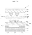
- FIG. 2 illustrates a modification of the LCD of FIG. 1 .
- an LCD 1A includes an in-cell polarizer IPA.
- the in-cell polarizer IPA includes a first substrate 30, a reflecting unit provided on one surface of the first substrate 30, and a wire grid polarizer 35 provided on another surface of the first substrate 30.
- the reflecting unit may include a first reflecting unit 25a provided in one region of a first surface 30a of the first substrate 30 and a second reflecting unit 25b provided in another region of the first surface 30a of the first substrate 30.
- the wire grid polarizer 35 may be provided in an opening-area OA between the first reflecting unit 25a and the second reflecting unit 25b.
- the first reflecting unit 25a and the second reflecting unit 25b may be provided in a non-opening area NOA corresponding to a region in which a first black matrix 45a and a second black matrix 45b are provided on an electrode layer 40.
- FIG. 2 since elements denoted by the same reference numerals as those of FIG. 1 actually have the same structures and perform the same operations as those of FIG. 1 , repeated description thereof will not be given.
- FIG. 2 an example is illustrated in which the first and second reflecting units 25a and 25b are provided and correspond to the non-opening area NOA in which the first and second black matrices 45a and 45b are provided.
- FIG. 3 illustrates another modification of the LCD of FIG. 1 .
- an LCD 1C includes an in-cell polarizer IP.
- the in-cell polarizer IP may include a first substrate 30, a reflecting unit 25 provided on one surface of the first substrate 30, and a wire grid polarizer 35C provided on another surface of the first substrate 30.
- the reflecting unit 25 may be provided in a non-opening area NOA where a black matrix 45 is provided.
- the wire grid polarizer 35C may be provided on an entire second surface 30b of the first substrate 30.
- the wire grid polarizer 35C is provided on the entire second surface 30b so that manufacturing processes may be simplified in comparison with a case in which the wire grid polarizer 35C is provided in a partial region of the second surface 30b.
- the in-cell polarizer IP illustrated in FIG. 4 includes a first substrate 30, a wire grid polarizer 35 provided on a first surface 30a of the first substrate 30, and a reflecting unit 25 provided on a second surface 30b of the first substrate 30.
- a first substrate 30 a wire grid polarizer 35 provided on a first surface 30a of the first substrate 30, and a reflecting unit 25 provided on a second surface 30b of the first substrate 30.
- the reflecting unit 25 is provided on an upper surface of the first substrate 30 and the wire grid polarizer 35 is provided on a lower surface of the first substrate 30.
- the in-cell polarizer IP illustrated in FIG. 5 includes a first substrate 30, a wire grid polarizer 35 provided on a first surface 30a of the first substrate 30, and a reflecting unit 25 provided on a second surface 30b of the first substrate 30.
- a wire grid polarizer 35 is provided on the entire first surface 30a of the first substrate 30.
- the in-cell polarizer IP illustrated in FIG. 6 includes a first substrate 30, a reflecting unit 25-1 provided on a first surface 30a of the first substrate 30, and a wire grid polarizer 35 provided on a second surface 30b of the first substrate 30.
- the reflecting unit 25-1 may include at least one tilted side surface 26.
- the reflecting unit 25-1 may have a trapezoidal cross-section, for example.
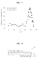
- FIG. 7 illustrates a change in average illumination measured in terms of lux (lx) according to a tilt angle ⁇ in degrees (°) of the side surface 26 of the reflecting unit 25-1 in FIG. 6 .
- FIG. 7 illustrates simulation results when heights h of the reflecting unit 25-1 are 16 micrometers ( ⁇ m) and 8 ⁇ m.
- the average illumination is relatively high when the tilt angle ⁇ of the side surface 26 of the reflecting unit 25-1 is, for example, in the range of about 60 degrees to about 80 degrees.
- the average illumination may be higher than when the reflecting unit 25-1 has a side surface that has a right angle with the first surface 30a.
- the in-cell polarizer IP illustrated in FIG. 8 includes a first substrate 30, a reflecting unit 25-2 provided on a first surface 30a of the first substrate 30, and a wire grid polarizer 35 provided on a second surface 30b of the first substrate 30.
- the reflecting unit 25-2 may have an array structure.
- a plurality of unit bodies 25-2a may be arranged in a one-dimensional array structure.
- the unit bodies 25-2a may have various shapes.
- the unit bodies 25-2a may have polygonal cross-sections.
- the unit bodies 25-2a may have, for example, square cross-sections, trapezoidal cross-sections, or triangular cross-sections.
- a reflecting unit 25-3 may include unit bodies 25-3a having semicircular cross-sections.
- the unit bodies 25-3a may be, for example, semi-cylindrical, for example.
- the unit bodies 25-3a may be arranged in a one-dimensional array structure.
- a reflecting unit 25-4 may have a two-dimensional array structure.
- the reflecting unit 25-4 may have a plurality of unit bodies 25-4a and the plurality of unit bodies 25-4a may be arranged in the two-dimensional array structure.
- the unit bodies 25-4a may be arranged to be separate from each other or to contact each other.
- the unit bodies 25-4a may have various shapes.
- the unit bodies 25-4a may have polygonal cross-sections, for example.
- the unit bodies 25-4a may have, for example, square cross-sections or trapezoidal cross-sections.
- a reflecting unit 25-5 may include spherical unit bodies 25-5a, for example.
- the unit bodies 25-5a may be arranged in a two-dimensional array structure, for example.
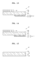
- FIG. 13 illustrates another example of the in-cell polarizer IP.
- the in-cell polarizer IP includes a first substrate 30, a reflecting unit 25-6 provided on a first surface 30a of the first substrate 30, and a wire grid polarizer 35 provided on a second surface 30b of the first substrate 30.
- the reflecting unit 25-6 may include a body 25-6a and an uneven unit 25-6b provided on the body 25-6a.
- the body 25-6a may have a cross-section with various shapes. In an exemplary embodiment, the body 25-6a may have a polygonal cross-section, for example.
- the body 25-6a may have a trapezoidal cross-section. Reflection efficiency may be improved by the uneven unit 25-6b.
- the in-cell polarizer IP illustrated in FIG. 14 includes a first substrate 30, a reflecting unit 25-7 provided on a first surface 30a of the first substrate 30, and a wire grid polarizer 35 provided on a second surface 30b of the first substrate 30.
- the reflecting unit 25-7 may include a body 25-7a and an uneven unit 25-7b provided on the body 25-7a.
- the body 25-7a may have, for example, a square cross-section, for example.
- FIGS. 6 to 14 illustrate the examples of the in-cell polarizer, in which the reflecting unit is provided on the first surface of the first substrate.
- the reflecting unit may be provided on the second surface of the first substrate.
- the light source unit 20 is disposed and the in-cell polarizer IP is disposed on the light source unit 20.
- the in-cell polarizer IP is manufactured, a process for an upper portion of the first substrate 30 and a process for a lower portion of the first substrate 30 may be separately performed.
- the reflecting unit 25 may be disposed on one surface, for example, the first surface 30a of the first substrate 30, and the wire grid polarizer 35 may be disposed on another surface, for example, the second surface 30b of the first substrate 30.
- the reflecting unit 25 may be provided by a photolithography method, for example.
- a metal layer 23 is deposited on the first surface 30a of the first substrate 30 and a photolithography process using a mask is performed to provide a pattern for the reflecting unit 25.
- the metal layer 23 is etched in accordance with the pattern to expose a part of the first surface 30a of the first substrate 30 and to provide the reflecting unit 25 in a remaining region.
- the pattern may vary in accordance with the pattern of the black matrix provided on the electrode layer 40.
- the metal layer in a region corresponding to the opening area OA (refer to FIG.
- the metal layer 23 may include at least one of Al, Ag, Au, and Pt, for example.
- wet etching or dry etching may be used as an etching method, for example.
- an etching condition such as etching time or etching solution is controlled to control a shape and size of the reflecting unit 25.
- the wire grid polarizer 35 is disposed on the second surface 30b of the first substrate 30.
- the wire grid polarizer 35 may be provided by one of a nanoimprint method, a block-copolymer lithography method, an e-beam lithography method, and a glancing angle deposition method.
- the reflecting unit 25 and the wire grid polarizer 35 are disposed on different surfaces of the first substrate by independent processes, after the reflecting unit 25 is provided, when the wire grid polarizer 35 is manufactured, an additional process for protecting the reflecting unit 25 is not required. Therefore, the manufacturing processes of the in-cell polarizer may be simplified and manufacturing cost thereof may be reduced.
- the electrode layer 40 is disposed above the first substrate 30, and the second substrate 50 is provided to be separated from the electrode layer 40.
- the electrode layer 40 is disposed and the black matrix 45 may be disposed thereon.
- the polarizing plate 55 is disposed on one surface of the second substrate 50.
- the LC layer 48 may be provided between the electrode layer 40 and the second substrate 50.
Landscapes
- Physics & Mathematics (AREA)
- Nonlinear Science (AREA)
- General Physics & Mathematics (AREA)
- Optics & Photonics (AREA)
- Mathematical Physics (AREA)
- Chemical & Material Sciences (AREA)
- Crystallography & Structural Chemistry (AREA)
- Polarising Elements (AREA)
- Liquid Crystal (AREA)
Abstract
Description
- Exemplary embodiments of the invention relate to an in-cell polarizer capable of simplifying manufacturing processes, a liquid crystal display ("LCD") including the same, and a method of manufacturing an LCD.
- In various application fields, in order to control light emitted from a light source, a polarization characteristic of the light is used. In the case of a liquid crystal display ("LCD") using a liquid crystal ("LC") panel, for example, LC molecules change a polarization direction of linear polarization in the LC panel so that the LC panel functions as a shutter for transmitting or blocking light. The LCD includes first and second polarizing plates having polarization directions which are orthogonal to each other, and an LC layer provided between the first and second polarizing plates. Each of pixels in the LCD includes a thin film transistor ("TFT"). Whether a voltage is applied to each of the pixels is determined in accordance with a switching operation of the TFT. When the voltage is applied to the pixel, for example, the LC molecules are linearly aligned so that incident light passes through the LC layer with no change in polarization direction thereof, and is blocked by the second polarizing plate. When the voltage is not applied to the pixel, the LC molecules are twisted so that incident light passes through the LC layer due to a change in polarization direction thereof in accordance with an arrangement of the LC molecules and passes through the second polarizing plate. That is, white is displayed when LC molecules are twisted and black is displayed when the LC molecules are linearly aligned.
- Since use efficiency of light by polarizing plates is low, light efficiency of a liquid crystal display ("LCD") deteriorates.
- Provided is an in-cell polarizer capable of simplifying manufacturing processes.
- Provided is an LCD capable of simplifying manufacturing processes.
- Provided is a method of manufacturing an LCD capable of simplifying manufacturing processes.
- Exemplary embodiments will be set forth in part in the description which follows and, in part, will be apparent from the description, or may be learned by practice of the presented embodiments.
- According to an exemplary embodiment of the invention, an LCD includes a light source unit, a first substrate provided on the light source unit, an electrode layer provided on the first substrate, a second substrate separate from the electrode layer, a polarizing plate provided on a surface of the second substrate, a liquid crystal ("LC") layer disposed between the electrode layer and the second substrate, a reflecting unit provided on a surface of the first substrate, and a wire grid polarizer provided on an opposite surface of the first substrate.
- In an exemplary embodiment, the first substrate may include a first surface facing the light source unit and a second surface facing the electrode layer, the reflecting unit may be provided on the first surface of the first substrate, and the wire grid polarizer may be provided on the second surface of the first substrate.
- In an exemplary embodiment, the electrode layer may include a black matrix and the reflecting unit may be arranged in a position corresponding to the black matrix.
- In an exemplary embodiment, the wire grid polarizer may be arranged in a position corresponding to an opening area in which the electrode layer is exposed by the black matrix.
- In an exemplary embodiment, the wire grid polarizer may be provided in an entire or partial region of the opposite surface of the first substrate.
- In an exemplary embodiment, the reflecting unit may have at least one tilted side surface in a cross section.
- In an exemplary embodiment, the reflecting unit may include a plurality of unit bodies.
- In an exemplary embodiment, the plurality of unit bodies each may have at least one tilted side surface and the plurality of unit bodies may be arranged in a one-dimensional array structure or a two-dimensional array structure.
- In an exemplary embodiment, the plurality of unit bodies each may have at least one of trapezoidal cross-sections, semicircular cross-sections, and triangular cross-sections.
- In an exemplary embodiment, the reflecting unit may include a body and an uneven unit provided on the body.
- In an exemplary embodiment, the body may have a square cross-section or a trapezoidal cross-section.
- According to another exemplary embodiment of the invention, an in-cell polarizer includes a substrate, a reflecting unit provided on a surface of the substrate, and a wire grid polarizer provided on another surface of the substrate.
- A region in which the reflecting unit is provided and a region in which the wire grid polarizer is provided may partially overlap or may be separated from each other in a plan view.
- According to another exemplary embodiment of the invention, a method of manufacturing an LCD includes forming a light source unit, forming a first substrate on the light source unit, forming a reflecting unit on a surface of the first substrate, forming a wire grid polarizer on an opposite surface of the first substrate in a process independent from a process of forming the reflecting unit, forming an electrode layer on the first substrate, forming a second substrate to be separate from the electrode layer, forming a polarizing plate on a surface of the second substrate, and forming an LC layer between the electrode layer and the second substrate.
- In an exemplary embodiment, the wire grid polarizer may be provided by one of a nanoimprint method, a block-copolymer lithography method, an e-beam lithography method, and a glancing angle deposition method.
- In an exemplary embodiment, the reflecting unit may be provided by a photolithography method.
- These and/or other exemplary embodiments will become apparent and more readily appreciated from the following description of the embodiments, taken in conjunction with the accompanying drawings, in which:
-
FIG. 1 schematically illustrates an exemplary embodiment of a liquid crystal display ("LCD") according to the invention; -
FIG. 2 illustrates a modification of the LCD ofFIG. 1 ; -
FIG. 3 illustrates another modification of the LCD ofFIG. 1 ; -
FIGS. 4 to 6 illustrate examples of an exemplary embodiment of an in-cell polarizer according to the invention; -
FIG. 7 illustrates a change in average illumination according to a slope of a side surface of a reflecting unit of the in-cell polarizer ofFIG. 6 ; -
FIGS. 8 to 14 illustrate examples of an exemplary embodiment of an in-cell polarizer according to the invention; and -
FIGS. 15 to 17 illustrate an exemplary embodiment of a method of manufacturing an LCD according to the invention. - Exemplary embodiments of the invention now will be described more fully hereinafter with reference to the accompanying drawings, in which various embodiments are shown. Exemplary embodiments of the invention may, however, be embodied in many different forms, and should not be construed as limited to the embodiments set forth herein. Rather, these embodiments are provided so that exemplary embodiments of the invention will be thorough and complete, and will fully convey the scope of the invention to those skilled in the art. Like reference numerals refer to like elements throughout.
- It will be understood that when an element is referred to as being "on" another element, it can be directly on the other element or intervening elements may be therebetween. In contrast, when an element is referred to as being "directly on" another element, there are no intervening elements present.
- Reference will now be made in detail to embodiments, examples of which are illustrated in the accompanying drawings, wherein like reference numerals refer to like elements throughout. In this regard, the embodiments may have different forms and should not be construed as being limited to the descriptions set forth herein. In the drawings, the thickness of layers and regions are exaggerated for clarity. It will also be understood that when an element is referred to as being "on" another element, it can be directly on the other element, or intervening elements may also be present.
- It will be understood that, although the terms "first," "second," "third" etc. may be used herein to describe various elements, components, regions, layers and/or sections, these elements, components, regions, layers and/or sections should not be limited by these terms. These terms are only used to distinguish one element, component, region, layer or section from another element, component, region, layer or section. Thus, "a first element," "component," "region," "layer" or "section" discussed below could be termed a second element, component, region, layer or section without departing from the teachings herein.
- The terminology used herein is for the purpose of describing particular embodiments only and is not intended to be limiting. As used herein, the singular forms "a," "an," and "the" are intended to include the plural forms, including "at least one," unless the content clearly indicates otherwise. "Or" means "and/or." As used herein, the term "and/or" includes any and all combinations of one or more of the associated listed items. It will be further understood that the terms "comprises" and/or "comprising," or "includes" and/or "including" when used in this specification, specify the presence of stated features, regions, integers, steps, operations, elements, and/or components, but do not preclude the presence or addition of one or more other features, regions, integers, steps, operations, elements, components, and/or groups thereof.
- Furthermore, relative terms, such as "lower" or "bottom" and "upper" or "top," may be used herein to describe one element's relationship to another element as illustrated in the Figures. It will be understood that relative terms are intended to encompass different orientations of the device in addition to the orientation depicted in the Figures. In an exemplary embodiment, when the device in one of the figures is turned over, elements described as being on the "lower" side of other elements would then be oriented on "upper" sides of the other elements. The exemplary term "lower," can therefore, encompasses both an orientation of "lower" and "upper," depending on the particular orientation of the figure. Similarly, when the device in one of the figures is turned over, elements described as "below" or "beneath" other elements would then be oriented "above" the other elements. The exemplary terms "below" or "beneath" can, therefore, encompass both an orientation of above and below.
- "About" or "approximately" as used herein is inclusive of the stated value and means within an acceptable range of deviation for the particular value as determined by one of ordinary skill in the art, considering the measurement in question and the error associated with measurement of the particular quantity (i.e., the limitations of the measurement system). For example, "about" can mean within one or more standard deviations, or within ± 30%, 20%, 10%, 5% of the stated value.
- Unless otherwise defined, all terms (including technical and scientific terms) used herein have the same meaning as commonly understood by one of ordinary skill in the art to which exemplary embodiments of invention belongs. It will be further understood that terms, such as those defined in commonly used dictionaries, should be interpreted as having a meaning that is consistent with their meaning in the context of the relevant art and the exemplary embodiments of invention, and will not be interpreted in an idealized or overly formal sense unless expressly so defined herein.
- Exemplary embodiments are described herein with reference to cross section illustrations that are schematic illustrations of idealized embodiments. As such, variations from the shapes of the illustrations as a result, for example, of manufacturing techniques and/or tolerances, are to be expected. Thus, embodiments described herein should not be construed as limited to the particular shapes of regions as illustrated herein but are to include deviations in shapes that result, for example, from manufacturing. In an exemplary embodiment, a region illustrated or described as flat may, typically, have rough and/or nonlinear features. Moreover, sharp angles that are illustrated may be rounded. Thus, the regions illustrated in the figures are schematic in nature and their shapes are not intended to illustrate the precise shape of a region and are not intended to limit the scope of the claims.
- Hereinafter, an in-cell polarizer, a liquid crystal display ("LCD"), and a method of manufacturing an LCD according to an exemplary embodiment of the invention will be described in detail with reference to the accompanying drawings.
-
FIG. 1 schematically illustrates anLCD 1 according to an exemplary embodiment of the invention. TheLCD 1 includes alight source unit 20 and an in-cell polarizer IP for reflecting and transmitting some light emitted from thelight source unit 20. - An
electrode layer 40 and asecond substrate 50 are separately arranged above the in-cell polarizer IP. A liquid crystal ("LC")layer 48 may be provided between theelectrode layer 40 and thesecond substrate 50. Apolarizing plate 55 may be provided on one surface of thesecond substrate 50. - A reflecting
plate 10 may be further provided below thelight source unit 20. - In an exemplary embodiment, the
light source unit 20 may be classified as either a direct light type light source unit or an edge light type light source unit in accordance with an arrangement of a light source with respect to thelight source unit 20. In the direct light type light source unit, the light source is provided below the in-cell polarizer IP so that light is directly irradiated on the LCD. In the edge light type light source unit, light is irradiated on the in-cell polarizer IP through a light guide plate (not shown). Both the direct light type light source unit and the edge light type light source unit may be applied to the LCD according to the exemplary embodiment of the invention. In an exemplary embodiment, a light emitting diode ("LED"), an organic light emitting diode ("OLED"), and a cool cathode fluorescent light ("CCFL") may be used as the light source of thelight source unit 20. However, the light source of thelight source unit 20 is not limited thereto, and various other types of light sources may be used. - The in-cell polarizer IP may include a
first substrate 30, a reflectingunit 25 provided on one surface of thefirst substrate 30, and awire grid polarizer 35 provided on another surface of thefirst substrate 30. In an exemplary embodiment, thefirst substrate 30 may be a transparent substrate that transmits light. In an exemplary embodiment, thefirst substrate 30 may be, for example, a glass substrate or a transparent plastic substrate. The reflectingunit 25 and thewire grid polarizer 35 may be provided on different surfaces of thefirst substrate 30. Thefirst substrate 30 may include afirst surface 30a facing thelight source unit 20 and asecond surface 30b facing away from thelight source unit 20. In an exemplary embodiment, the reflectingunit 25 may be provided on thefirst surface 30a and thewire grid polarizer 35 may be provided on thesecond surface 30b. In another exemplary embodiment, the reflectingunit 25 may be provided on thesecond surface 30b and thewire grid polarizer 35 may be provided on thefirst surface 30a. - The reflecting
unit 25 may include a material that reflects light. In an exemplary embodiment, the reflectingunit 25 may include, for example, metal. In an exemplary embodiment, the reflectingunit 25 may include at least one of aluminum (Al), silver (Ag), gold (Au), and platinum (Pt), for example. The reflectingunit 25 may be provided in a partial region of thefirst substrate 30. In an exemplary embodiment, the reflectingunit 25 may be provided in a region corresponding to ablack matrix 45 provided on theelectrode layer 40. - The
LCD 1 includes a plurality of pixels, and one pixel may display one color or a plurality of colors. In an exemplary embodiment, one pixel may include three sub-pixels that display a plurality of colors, for example, red, green, and blue. In theLCD 1 ofFIG. 1 , one pixel or one sub pixel is illustrated. TheLCD 1 may include, for example, an opening area OA that transmits light and a non-opening area NOA that does not transmit light. - The
black matrix 45 may be provided on a part of theelectrode layer 40 and may be arranged in accordance with an electrode pattern of theelectrode layer 40. Theblack matrix 45 may be provided in order to prevent the electrode pattern from affecting an image. In an exemplary embodiment, a region in which theblack matrix 45 is arranged may be the non-opening area NOA that does not transmit light and a remaining region may be the opening area OA that transmits light. The reflectingunit 25 may be provided in the non-opening area NOA and thewire grid polarizer 35 may be provided in the opening area OA. When the reflectingunit 25 is arranged in the non-opening area NOA, light efficiency may be improved. However, an exemplary embodiment of the invention is not limited thereto. In another exemplary embodiment, in a plan view, the reflectingunit 25 may be arranged in a region larger than the non-opening area NOA, and thewire grid polarizer 35 may be arranged in a region larger than that including the opening area OA. That is, the region in which the reflectingunit 25 is provided and the region in which thewire grid polarizer 35 is provided may not overlap or may partially overlap. - In the
wire grid polarizer 35,wires 35a may be arranged on thefirst substrate 30 such that thewires 35a are separated from each other by a predetermined distance. In an exemplary embodiment, an arrangement period of thewires 35a may be smaller than a wavelength of incident light.Grooves 35b may be defined betweenadjacent wires 35a. A pitch between thewires 35a may be no more than a quarter of the wavelength of the incident light. In an exemplary embodiment, the pitch between wires may be larger than 0 and no more than about 200 nanometers (nm). A fill factor of thewire grid polarizer 35 may be no less than about 0.3 and smaller than about 1. The fill factor represents a cross-sectional area ratio between thewire 35a and thegroove 35b. A height of thewire 35a taken along a vertical direction in a cross section may be no less than about 100 nm, and, for example, an aspect ratio of thewire 35a may be no less than about 1. - In an exemplary embodiment, the
wire 35a may include metal, for example, at least one of Al, Ag, Au, copper (Cu), nickel (Ni), and Pt. - In an exemplary embodiment, the
wire grid polarizer 35 may transmit only light of first polarization of the incident light and may reflect light of second polarization of the incident light, for example. The first polarization may be P polarization and the second polarization may be S polarization. - In an exemplary embodiment, since the reflecting
unit 25 and thewire grid polarizer 35 are provided on different surfaces of thefirst substrate 30, the reflectingunit 25 and thewire grid polarizer 35 may be manufactured by independent processes. As described above, the manufacturing processes of the reflectingunit 25 and thewire grid polarizer 35 may be separately performed to simplify manufacturing processes of the in-cell polarizer IP. When the reflectingunit 25 is manufactured in the same surface of the substrate as that of thewire grid polarizer 35, after thewire grid polarizer 35 is manufactured, since a process for protecting thewire grid polarizer 35 must be additionally performed while manufacturing the reflectingunit 25, the manufacturing processes of the in-cell polarizer may be very complicated. In addition, a position or the manufacturing processes of the reflectingunit 25 may vary in accordance with a pattern of theblack matrix 45. Manufacturing processes of thewire grid polarizer 35 may become complicated in accordance with changes in the manufacturing processes of the reflectingunit 25. Since the reflectingunit 25 and thewire grid polarizer 35 may be arranged on different surfaces of the substrate to independently manufacture the reflectingunit 25 and thewire grid polarizer 35, the manufacturing processes of the in-cell polarizer may be simplified. - The
electrode layer 40 may be provided above the in-cell polarizer IP. In an exemplary embodiment, theelectrode layer 40 may include a pixel electrode for driving theLC layer 48 and a thin film transistor ("TFT") for applying voltage to the pixel electrode, for example. - In an exemplary embodiment, the
second substrate 50 may be a transparent substrate that transmits light and may be used as an electrode layer. In an exemplary embodiment, thesecond substrate 50 may include a transparent oxide semiconductor material. In an exemplary embodiment, thesecond substrate 50 may include a transparent conductive material such as indium tin oxide ("ITO"), indium zinc oxide ("IZO"), ZnO, and In2O3. - The
polarizing plate 55 may be provided on one surface of thesecond substrate 50. In an exemplary embodiment, thepolarizing plate 55 may be provided on an upper or lower surface of thesecond substrate 50. In an exemplary embodiment, thepolarizing plate 55 may be an absorbing type polarizing plate or a reflecting type polarizing plate, for example. When thepolarizing plate 55 is the reflecting type polarizing plate, thepolarizing plate 55 may be, for example, a wire grid polarizing plate. - Next, operation of the LCD1 will be described.
- Light is emitted from the
light source unit 20 and is incident on the in-cell polarizer IP. Of the light incident on the in-cell polarizer IP, light incident on the reflectingunit 25 may be reflected to thelight source unit 20 and light incident on a region excluding the reflectingunit 25 may pass through thefirst substrate 30 and then be reflected or transmitted by thewire grid polarizer 35 in a polarization direction. In an exemplary embodiment, the light of the P polarization may be transmitted and the light of the S polarization may be reflected. - The light reflected by the reflecting
unit 25 and the light reflected by thewire grid polarizer 35 may be reflected by thelight source unit 20 or a reflectingplate 10 back to the in-cell polarizer IP so as to be re-incident on the in-cell polarizer IP. The re-incident light is recycled by repeating the above processes so that light efficiency may be improved. In the case where the reflectingunit 25 is arranged on thefirst surface 30a of thefirst substrate 30, a recycling rate of light is higher than when the reflectingunit 25 is reflected to thesecond surface 30b of thefirst substrate 30. When the reflectingunit 25 is arranged to be closer to thelight source unit 20, the recycling rate of the light may be higher. - The light that passes through the in-cell polarizer IP is incident on the
LC layer 48. A voltage is applied between theelectrode layer 40 and thesecond substrate 50, and transmittance of the light may be controlled in accordance with the magnitude of the applied voltage. Grayscales may be displayed by controlling the transmittance of the light. In an exemplary embodiment, thepolarizing plate 55 may have a polarization direction that is perpendicular to the polarization direction of thewire grid polarizer 35. In an exemplary embodiment, thepolarizing plate 55 may transmit, for example, the light of the S polarization. - As described above, each pixel may control transmittance of light to display an image. A color filter may be provided to display a color image.
- Next,
FIG. 2 illustrates a modification of the LCD ofFIG. 1 . - As illustrated in
FIG. 2 , an LCD 1A includes an in-cell polarizer IPA. The in-cell polarizer IPA includes afirst substrate 30, a reflecting unit provided on one surface of thefirst substrate 30, and awire grid polarizer 35 provided on another surface of thefirst substrate 30. The reflecting unit may include a first reflectingunit 25a provided in one region of afirst surface 30a of thefirst substrate 30 and a second reflectingunit 25b provided in another region of thefirst surface 30a of thefirst substrate 30. Thewire grid polarizer 35 may be provided in an opening-area OA between the first reflectingunit 25a and the second reflectingunit 25b. The first reflectingunit 25a and the second reflectingunit 25b may be provided in a non-opening area NOA corresponding to a region in which a firstblack matrix 45a and a secondblack matrix 45b are provided on anelectrode layer 40. - In
FIG. 2 , since elements denoted by the same reference numerals as those ofFIG. 1 actually have the same structures and perform the same operations as those ofFIG. 1 , repeated description thereof will not be given. InFIG. 2 , an example is illustrated in which the first and second reflectingunits black matrices -
FIG. 3 illustrates another modification of the LCD ofFIG. 1 . As illustrated inFIG. 3 , anLCD 1C includes an in-cell polarizer IP. The in-cell polarizer IP may include afirst substrate 30, a reflectingunit 25 provided on one surface of thefirst substrate 30, and awire grid polarizer 35C provided on another surface of thefirst substrate 30. The reflectingunit 25 may be provided in a non-opening area NOA where ablack matrix 45 is provided. Thewire grid polarizer 35C may be provided on an entiresecond surface 30b of thefirst substrate 30. Thewire grid polarizer 35C is provided on the entiresecond surface 30b so that manufacturing processes may be simplified in comparison with a case in which thewire grid polarizer 35C is provided in a partial region of thesecond surface 30b. This is because, when thewire grid polarizer 35C is provided in the partial region, a process of etching another partial region in which thewire grid polarizer 35C is not required is added. However, the etching process is not required for the structure illustrated inFIG. 3 . - Next, various examples of the in-cell polarizer IP will be described.
- The in-cell polarizer IP illustrated in
FIG. 4 includes afirst substrate 30, awire grid polarizer 35 provided on afirst surface 30a of thefirst substrate 30, and a reflectingunit 25 provided on asecond surface 30b of thefirst substrate 30. InFIG. 4 , an example is illustrated in which the reflectingunit 25 is provided on an upper surface of thefirst substrate 30 and thewire grid polarizer 35 is provided on a lower surface of thefirst substrate 30. - The in-cell polarizer IP illustrated in
FIG. 5 includes afirst substrate 30, awire grid polarizer 35 provided on afirst surface 30a of thefirst substrate 30, and a reflectingunit 25 provided on asecond surface 30b of thefirst substrate 30. InFIG. 5 , an example is illustrated in which thewire grid polarizer 35 is provided on the entirefirst surface 30a of thefirst substrate 30. - The in-cell polarizer IP illustrated in
FIG. 6 includes afirst substrate 30, a reflecting unit 25-1 provided on afirst surface 30a of thefirst substrate 30, and awire grid polarizer 35 provided on asecond surface 30b of thefirst substrate 30. The reflecting unit 25-1 may include at least one tiltedside surface 26. In an exemplary embodiment, the reflecting unit 25-1 may have a trapezoidal cross-section, for example.FIG. 7 illustrates a change in average illumination measured in terms of lux (lx) according to a tilt angle θ in degrees (°) of theside surface 26 of the reflecting unit 25-1 inFIG. 6 .FIG. 7 illustrates simulation results when heights h of the reflecting unit 25-1 are 16 micrometers (µm) and 8 µm. The average illumination is relatively high when the tilt angle θ of theside surface 26 of the reflecting unit 25-1 is, for example, in the range of about 60 degrees to about 80 degrees. - When the reflecting unit 25-1 has a side surface tilted with respect to the
first surface 30a, the average illumination may be higher than when the reflecting unit 25-1 has a side surface that has a right angle with thefirst surface 30a. - Next, the in-cell polarizer IP illustrated in
FIG. 8 includes afirst substrate 30, a reflecting unit 25-2 provided on afirst surface 30a of thefirst substrate 30, and awire grid polarizer 35 provided on asecond surface 30b of thefirst substrate 30. The reflecting unit 25-2 may have an array structure. In an exemplary embodiment, in the reflecting unit 25-2, as illustrated inFIG. 9 , a plurality of unit bodies 25-2a may be arranged in a one-dimensional array structure. The unit bodies 25-2a may have various shapes. In an exemplary embodiment, the unit bodies 25-2a may have polygonal cross-sections. The unit bodies 25-2a may have, for example, square cross-sections, trapezoidal cross-sections, or triangular cross-sections. - As illustrated in
FIG. 10 , a reflecting unit 25-3 may include unit bodies 25-3a having semicircular cross-sections. In an exemplary embodiment, the unit bodies 25-3a may be, for example, semi-cylindrical, for example. In an exemplary embodiment, the unit bodies 25-3a may be arranged in a one-dimensional array structure. - Next, in the in-cell polarizer IP illustrated in
FIG. 11 , a reflecting unit 25-4 may have a two-dimensional array structure. The reflecting unit 25-4 may have a plurality of unit bodies 25-4a and the plurality of unit bodies 25-4a may be arranged in the two-dimensional array structure. The unit bodies 25-4a may be arranged to be separate from each other or to contact each other. The unit bodies 25-4a may have various shapes. In an exemplary embodiment, the unit bodies 25-4a may have polygonal cross-sections, for example. In exemplary embodiments, the unit bodies 25-4a may have, for example, square cross-sections or trapezoidal cross-sections. - As illustrated in
FIG. 12 , a reflecting unit 25-5 may include spherical unit bodies 25-5a, for example. In an exemplary embodiment, the unit bodies 25-5a may be arranged in a two-dimensional array structure, for example. -
FIG. 13 illustrates another example of the in-cell polarizer IP. The in-cell polarizer IP includes afirst substrate 30, a reflecting unit 25-6 provided on afirst surface 30a of thefirst substrate 30, and awire grid polarizer 35 provided on asecond surface 30b of thefirst substrate 30. The reflecting unit 25-6 may include a body 25-6a and an uneven unit 25-6b provided on the body 25-6a. The body 25-6a may have a cross-section with various shapes. In an exemplary embodiment, the body 25-6a may have a polygonal cross-section, for example. The body 25-6a may have a trapezoidal cross-section. Reflection efficiency may be improved by the uneven unit 25-6b. - The in-cell polarizer IP illustrated in
FIG. 14 includes afirst substrate 30, a reflecting unit 25-7 provided on afirst surface 30a of thefirst substrate 30, and awire grid polarizer 35 provided on asecond surface 30b of thefirst substrate 30. The reflecting unit 25-7 may include a body 25-7a and an uneven unit 25-7b provided on the body 25-7a. In an exemplary embodiment, the body 25-7a may have, for example, a square cross-section, for example. -
FIGS. 6 to 14 illustrate the examples of the in-cell polarizer, in which the reflecting unit is provided on the first surface of the first substrate. However, the reflecting unit may be provided on the second surface of the first substrate. - Next, a method of manufacturing an LCD according to an exemplary embodiment of the invention will be described. In the method of manufacturing the LCD, referring to
FIG. 1 , thelight source unit 20 is disposed and the in-cell polarizer IP is disposed on thelight source unit 20. When the in-cell polarizer IP is manufactured, a process for an upper portion of thefirst substrate 30 and a process for a lower portion of thefirst substrate 30 may be separately performed. In an exemplary embodiment, the reflectingunit 25 may be disposed on one surface, for example, thefirst surface 30a of thefirst substrate 30, and thewire grid polarizer 35 may be disposed on another surface, for example, thesecond surface 30b of thefirst substrate 30. - Processes of manufacturing the reflecting
unit 25 will be described with reference toFIGS. 15 and16 . In an exemplary embodiment, the reflectingunit 25 may be provided by a photolithography method, for example. In an exemplary embodiment, ametal layer 23 is deposited on thefirst surface 30a of thefirst substrate 30 and a photolithography process using a mask is performed to provide a pattern for the reflectingunit 25. Themetal layer 23 is etched in accordance with the pattern to expose a part of thefirst surface 30a of thefirst substrate 30 and to provide the reflectingunit 25 in a remaining region. The pattern may vary in accordance with the pattern of the black matrix provided on theelectrode layer 40. The metal layer in a region corresponding to the opening area OA (refer toFIG. 1 ), in which the black matrix is not provided, is etched and the metal layer in a region corresponding to the non-opening area NOA (refer toFIG. 1 ), in which the black matrix is provided, is left to form the reflectingunit 25. In an exemplary embodiment, themetal layer 23 may include at least one of Al, Ag, Au, and Pt, for example. In exemplary embodiments, wet etching or dry etching may be used as an etching method, for example. Here, an etching condition such as etching time or etching solution is controlled to control a shape and size of the reflectingunit 25. - Next, as illustrated in
FIG. 17 , thewire grid polarizer 35 is disposed on thesecond surface 30b of thefirst substrate 30. Thewire grid polarizer 35 may be provided by one of a nanoimprint method, a block-copolymer lithography method, an e-beam lithography method, and a glancing angle deposition method. - Since the reflecting
unit 25 and thewire grid polarizer 35 are disposed on different surfaces of the first substrate by independent processes, after the reflectingunit 25 is provided, when thewire grid polarizer 35 is manufactured, an additional process for protecting the reflectingunit 25 is not required. Therefore, the manufacturing processes of the in-cell polarizer may be simplified and manufacturing cost thereof may be reduced. - Next, referring to
FIG. 1 , theelectrode layer 40 is disposed above thefirst substrate 30, and thesecond substrate 50 is provided to be separated from theelectrode layer 40. Theelectrode layer 40 is disposed and theblack matrix 45 may be disposed thereon. Thepolarizing plate 55 is disposed on one surface of thesecond substrate 50. TheLC layer 48 may be provided between theelectrode layer 40 and thesecond substrate 50. - It should be understood that the exemplary embodiments described therein should be considered in a descriptive sense only and not for purposes of limitation. Descriptions of features or exemplary embodiments within each embodiment should typically be considered as available for other similar features or exemplary embodiments in other embodiments.
- While one or more embodiments of the invention have been described with reference to the figures, it will be understood by those of ordinary skill in the art that various changes in form and details may be made therein.
Claims (15)
- An in-cell polarizer comprising:a substrate;a reflecting unit provided on a surface of the substrate; anda wire grid polarizer provided on an opposite surface of the substrate.
- The in-cell polarizer of claim 1, wherein a region in which the reflecting unit is provided and a region in which the wire grid polarizer is provided partially overlap or are separated from each other in a plan view.
- The in-cell polarizer of claim 1 or 2, wherein the reflecting unit is provided in a partial region of the substrate.
- The in-cell polarizer of claim 1, 2 or 3, wherein the reflecting unit has at least one tilted side surface in a cross section.
- The in-cell polarizer of any of claims 1 to 4, wherein the reflecting unit comprises a plurality of unit bodies.
- The in-cell polarizer of claim 5,
wherein each of the plurality of unit bodies has at least one tilted side surface in a cross section, and
wherein the plurality of unit bodies is arranged in a one-dimensional array structure or a two-dimensional array structure,
and preferably wherein each of the plurality of unit bodies has at least one of a trapezoidal cross-section, a semicircular cross-section, and a triangular cross-section. - The in-cell polarizer of any preceding claim, wherein the reflecting unit comprises:a body; andan uneven unit provided on the body.
- A liquid crystal display comprising:a light source unit;an in-cell polarizer according to any preceding claim, the substrate of the in-cell polarizer being a first substrate provided on the light source unit;an electrode layer provided on the first substrate;a second substrate separate from the electrode layer;a polarizing plate provided on a surface of the second substrate; anda liquid crystal layer disposed between the electrode layer and the second substrate.
- The liquid crystal display of claim 8,
wherein the first substrate comprises:a first surface facing the light source unit; anda second surface facing the electrode layer,wherein the reflecting unit is provided on the first surface of the first substrate,
andwherein the wire grid polarizer is provided on the second surface of the first substrate. - The liquid crystal display of claim 8 or 9,
wherein the electrode layer comprises a black matrix, and
wherein the reflecting unit is arranged in a position corresponding to the black matrix;
and preferably wherein the wire grid polarizer is provided in an entire or partial region of the opposite surface of the first substrate. - The liquid crystal display of claim 10, wherein the wire grid polarizer is arranged in a position corresponding to an opening area in which the electrode layer is exposed by the black matrix.
- The liquid crystal display of any of claims 8 to 11, wherein the reflecting unit has at least one tilted side surface in a cross section.
- The liquid crystal display of any of claims 8 to 12, wherein the reflecting unit comprises a plurality of unit bodies,
and preferably wherein each of the plurality of unit bodies has at least one tilted side surface in a cross section, and
wherein the plurality of unit bodies is arranged in a one-dimensional array structure or a two-dimensional array structure,
and preferably wherein each of the plurality of unit bodies has at least one of a trapezoidal cross-section, a semicircular cross-section, and a triangular cross-section. - A method of manufacturing a liquid crystal display, the method comprising:providing a light source unit;disposing a first substrate on the light source unit;disposing a reflecting unit on a surface of the first substrate;disposing a wire grid polarizer on an opposite surface of the first substrate in a process independent from a process of the disposing the reflecting unit;disposing an electrode layer on the first substrate;providing a second substrate to be separate from the electrode layer;disposing a polarizing plate on one surface of the second substrate; anddisposing a liquid crystal layer between the electrode layer and the second substrate,and preferably wherein the wire grid polarizer is provided by one of a nanoimprint method, a block-copolymer lithography method, an e-beam lithography method, and a glancing angle deposition method.and further preferably wherein the reflecting unit is provided by a photolithography method.
- The method of claim 14, wherein the first substrate comprises:a first surface facing the light source unit; anda second surface facing the electrode layer,wherein the reflecting unit is provided on the first surface of the first substrate,
andwherein the wire grid polarizer is provided on the second surface of the first substrate.
Applications Claiming Priority (1)
| Application Number | Priority Date | Filing Date | Title |
|---|---|---|---|
| KR1020140004061A KR102148417B1 (en) | 2014-01-13 | 2014-01-13 | In-cell polarizer, liquid crystal display having the same and method of manufacturing liquid crystal display |
Publications (2)
| Publication Number | Publication Date |
|---|---|
| EP2894511A1 true EP2894511A1 (en) | 2015-07-15 |
| EP2894511B1 EP2894511B1 (en) | 2018-03-14 |
Family
ID=52232114
Family Applications (1)
| Application Number | Title | Priority Date | Filing Date |
|---|---|---|---|
| EP15150428.9A Not-in-force EP2894511B1 (en) | 2014-01-13 | 2015-01-08 | In-cell polariser, liquid crystal display including it and method of manufacturing the liquid crystal display |
Country Status (5)
| Country | Link |
|---|---|
| US (1) | US9696589B2 (en) |
| EP (1) | EP2894511B1 (en) |
| JP (1) | JP6548212B2 (en) |
| KR (1) | KR102148417B1 (en) |
| CN (1) | CN104777659B (en) |
Families Citing this family (13)
| Publication number | Priority date | Publication date | Assignee | Title |
|---|---|---|---|---|
| KR20160056460A (en) | 2014-11-11 | 2016-05-20 | 삼성디스플레이 주식회사 | Curved display device |
| CN104730761A (en) * | 2015-04-08 | 2015-06-24 | 武汉华星光电技术有限公司 | Transflective liquid crystal display panel and transflective liquid crystal displayer |
| KR102415044B1 (en) | 2015-12-11 | 2022-07-01 | 삼성디스플레이 주식회사 | Touch screen panel, method of manufacturing the same and touch display apparatus |
| FI3401711T3 (en) * | 2016-01-08 | 2023-05-05 | Dainippon Printing Co Ltd | Diffractive optical element and light irradiation apparatus |
| CN105446001B (en) * | 2016-01-25 | 2018-09-04 | 京东方科技集团股份有限公司 | A kind of display panel and its working method, display device |
| KR102494859B1 (en) * | 2016-05-26 | 2023-02-02 | 삼성디스플레이 주식회사 | Display device and manufacturing method thereof |
| CN105807483B (en) | 2016-05-27 | 2019-01-22 | 京东方科技集团股份有限公司 | Display panel, manufacturing method thereof, and display device |
| SG11201900148YA (en) * | 2016-07-13 | 2019-02-27 | Scivax Corp | Optical element, light emitting element, optical device using said light emitting element, and method for producing said optical element |
| KR102609587B1 (en) * | 2016-07-19 | 2023-12-05 | 삼성디스플레이 주식회사 | Method of manufacturing imprint stamp and display apparatus manufactured using the imprint stamp |
| KR102654863B1 (en) * | 2016-11-08 | 2024-04-05 | 삼성전자주식회사 | Directional backlight unit, image display apparatus having the same |
| KR102377174B1 (en) | 2017-05-18 | 2022-03-21 | 엘지디스플레이 주식회사 | Liquid crystal display device |
| TWI687743B (en) * | 2018-12-11 | 2020-03-11 | 友達光電股份有限公司 | Display device and manufacturing method of polarizer structure |
| KR20220090079A (en) * | 2020-12-22 | 2022-06-29 | 에스케이하이닉스 주식회사 | Image Sensing Device |
Citations (6)
| Publication number | Priority date | Publication date | Assignee | Title |
|---|---|---|---|---|
| EP1180711A1 (en) * | 2000-01-28 | 2002-02-20 | Seiko Epson Corporation | Optical reflection polarizer and projector comprising the same |
| US20030072079A1 (en) * | 2001-10-15 | 2003-04-17 | Eastman Kodak Company | Double sided wire grid polarizer |
| US20080198302A1 (en) * | 2007-02-16 | 2008-08-21 | Samsung Electronics Co., Ltd. | Active reflective polarizer, liquid crystal display employing the same and method for the same |
| US20090170038A1 (en) * | 2007-12-27 | 2009-07-02 | Seiko Epson Corporation | Method for producing fine structure |
| JP2010210824A (en) * | 2009-03-09 | 2010-09-24 | Seiko Epson Corp | Optical element and illumination device |
| US20110222002A1 (en) * | 2010-03-10 | 2011-09-15 | Samsung Electronics Co., Ltd. | Liquid crystal display |
Family Cites Families (21)
| Publication number | Priority date | Publication date | Assignee | Title |
|---|---|---|---|---|
| JPH06138453A (en) * | 1992-10-26 | 1994-05-20 | Fujitsu Ltd | Liquid crystal display device |
| JPH0850283A (en) * | 1994-05-31 | 1996-02-20 | Sanyo Electric Co Ltd | Liquid crystal display panel |
| JP3663741B2 (en) * | 1996-05-22 | 2005-06-22 | セイコーエプソン株式会社 | Active matrix type liquid crystal display device and manufacturing method thereof |
| JP2000329916A (en) * | 1998-09-16 | 2000-11-30 | Sumitomo Chem Co Ltd | Transflective reflector |
| JP3884207B2 (en) | 2000-01-20 | 2007-02-21 | インターナショナル・ビジネス・マシーンズ・コーポレーション | Liquid crystal display |
| JP4618274B2 (en) * | 2001-07-13 | 2011-01-26 | セイコーエプソン株式会社 | Color filter substrate for liquid crystal display panel, liquid crystal display device, and electronic device |
| JP3989217B2 (en) * | 2001-10-10 | 2007-10-10 | 古河電気工業株式会社 | Light diffuse reflection sheet and surface light emitting device |
| JP3815461B2 (en) * | 2002-11-22 | 2006-08-30 | セイコーエプソン株式会社 | Liquid crystal display device and electronic device |
| JP4636886B2 (en) * | 2004-03-23 | 2011-02-23 | シチズンホールディングス株式会社 | Liquid crystal display device |
| JP4581450B2 (en) * | 2004-03-25 | 2010-11-17 | カシオ計算機株式会社 | Transflective liquid crystal display device. |
| CN100434995C (en) | 2004-04-15 | 2008-11-19 | 皇家飞利浦电子股份有限公司 | Transflective LCD display device |
| US7414784B2 (en) | 2004-09-23 | 2008-08-19 | Rohm And Haas Denmark Finance A/S | Low fill factor wire grid polarizer and method of use |
| KR20070050237A (en) | 2005-11-10 | 2007-05-15 | 엘지.필립스 엘시디 주식회사 | Backlight Unit for Liquid Crystal Display |
| JP4778873B2 (en) * | 2006-10-20 | 2011-09-21 | 株式会社 日立ディスプレイズ | Liquid crystal display |
| KR101282323B1 (en) * | 2006-10-26 | 2013-07-04 | 삼성디스플레이 주식회사 | Liquid crystal display |
| JP2009210725A (en) * | 2008-03-03 | 2009-09-17 | Seiko Epson Corp | Liquid crystal display device and electronic device |
| JP5255926B2 (en) * | 2008-07-02 | 2013-08-07 | 株式会社ジャパンディスプレイウェスト | Liquid crystal display device and manufacturing method thereof |
| US8865274B2 (en) * | 2010-04-02 | 2014-10-21 | Samsung Display Co., Ltd. | Liquid crystal display device, alignment film, and methods for manufacturing the same |
| KR101978312B1 (en) * | 2011-05-02 | 2019-05-15 | 삼성디스플레이 주식회사 | Liquid crystal device alignment layer and methods for manufacturing the same |
| KR20120032776A (en) | 2010-09-29 | 2012-04-06 | 엘지이노텍 주식회사 | A wire grid polarizer and backlightounit uaing the same |
| KR101878755B1 (en) * | 2012-11-20 | 2018-07-16 | 삼성전자주식회사 | Display panel having improved light-use efficiency, dispaly apparatus including the display panel, and method of fabricating the display panel |
-
2014
- 2014-01-13 KR KR1020140004061A patent/KR102148417B1/en not_active Expired - Fee Related
- 2014-10-24 US US14/522,787 patent/US9696589B2/en active Active
- 2014-12-09 CN CN201410748621.8A patent/CN104777659B/en active Active
-
2015
- 2015-01-08 EP EP15150428.9A patent/EP2894511B1/en not_active Not-in-force
- 2015-01-13 JP JP2015004314A patent/JP6548212B2/en active Active
Patent Citations (6)
| Publication number | Priority date | Publication date | Assignee | Title |
|---|---|---|---|---|
| EP1180711A1 (en) * | 2000-01-28 | 2002-02-20 | Seiko Epson Corporation | Optical reflection polarizer and projector comprising the same |
| US20030072079A1 (en) * | 2001-10-15 | 2003-04-17 | Eastman Kodak Company | Double sided wire grid polarizer |
| US20080198302A1 (en) * | 2007-02-16 | 2008-08-21 | Samsung Electronics Co., Ltd. | Active reflective polarizer, liquid crystal display employing the same and method for the same |
| US20090170038A1 (en) * | 2007-12-27 | 2009-07-02 | Seiko Epson Corporation | Method for producing fine structure |
| JP2010210824A (en) * | 2009-03-09 | 2010-09-24 | Seiko Epson Corp | Optical element and illumination device |
| US20110222002A1 (en) * | 2010-03-10 | 2011-09-15 | Samsung Electronics Co., Ltd. | Liquid crystal display |
Also Published As
| Publication number | Publication date |
|---|---|
| CN104777659B (en) | 2019-12-24 |
| KR20150084243A (en) | 2015-07-22 |
| JP2015132825A (en) | 2015-07-23 |
| JP6548212B2 (en) | 2019-07-24 |
| EP2894511B1 (en) | 2018-03-14 |
| KR102148417B1 (en) | 2020-08-27 |
| CN104777659A (en) | 2015-07-15 |
| US20150198833A1 (en) | 2015-07-16 |
| US9696589B2 (en) | 2017-07-04 |
Similar Documents
| Publication | Publication Date | Title |
|---|---|---|
| EP2894511B1 (en) | In-cell polariser, liquid crystal display including it and method of manufacturing the liquid crystal display | |
| KR102373327B1 (en) | Liquid crystal display device and method for driving the same | |
| US10698255B2 (en) | Photoluminescence device, method of manufacturing the same and display apparatus having the same | |
| US9703027B2 (en) | Wire grid polarizer, liquid crystal display having the same and method of manufacturing the same | |
| KR101336097B1 (en) | Liquid crystal display device having Wire grid polarizer | |
| US8068266B2 (en) | Display substrate, method of manufacturing the same and electrowetting display panel having the display substrate | |
| US8964276B2 (en) | Electro-wetting display apparatus | |
| US10473973B2 (en) | Display device | |
| US9519182B2 (en) | Display panel and method of manufacturing the same | |
| US10067375B2 (en) | Liquid crystal display device | |
| CN105929593A (en) | Array substrate, transparent display substrate and transparent display device | |
| KR20120025407A (en) | Liquid crystal display | |
| US20180188599A1 (en) | Display device | |
| KR102648614B1 (en) | Display apparatus | |
| US20160033701A1 (en) | Wire grid polarizer and method of fabricating the same | |
| CN101388365A (en) | Method for manufacturing display device | |
| KR101286004B1 (en) | Liquid crystal panel and liquid crystal display device having the same and method of manufacturing the same | |
| US8896792B2 (en) | Liquid crystal display device comprising a reactive mesogen that fixes liquid crystal molecules to form a liquid crystal domain | |
| TWI475287B (en) | Liquid crystal display devices and methods of manufacturing liquid crystal display devices | |
| US9740040B2 (en) | Display panel, display apparatus having the same and method of manufacturing the same | |
| CN104641283A (en) | Liquid crystal display device | |
| CN117199219A (en) | light emitting device | |
| CN209446923U (en) | Liquid crystal display panel | |
| US10989859B2 (en) | Backlight unit and display apparatus including the same | |
| CN118318204A (en) | Liquid crystal element, lighting device |
Legal Events
| Date | Code | Title | Description |
|---|---|---|---|
| PUAI | Public reference made under article 153(3) epc to a published international application that has entered the european phase |
Free format text: ORIGINAL CODE: 0009012 |
|
| 17P | Request for examination filed |
Effective date: 20150108 |
|
| AK | Designated contracting states |
Kind code of ref document: A1 Designated state(s): AL AT BE BG CH CY CZ DE DK EE ES FI FR GB GR HR HU IE IS IT LI LT LU LV MC MK MT NL NO PL PT RO RS SE SI SK SM TR |
|
| AX | Request for extension of the european patent |
Extension state: BA ME |
|
| RAP1 | Party data changed (applicant data changed or rights of an application transferred) |
Owner name: SAMSUNG DISPLAY CO., LTD. Owner name: SAMSUNG ELECTRONICS CO., LTD |
|
| R17P | Request for examination filed (corrected) |
Effective date: 20160115 |
|
| RBV | Designated contracting states (corrected) |
Designated state(s): AL AT BE BG CH CY CZ DE DK EE ES FI FR GB GR HR HU IE IS IT LI LT LU LV MC MK MT NL NO PL PT RO RS SE SI SK SM TR |
|
| 17Q | First examination report despatched |
Effective date: 20160512 |
|
| STAA | Information on the status of an ep patent application or granted ep patent |
Free format text: STATUS: EXAMINATION IS IN PROGRESS |
|
| GRAP | Despatch of communication of intention to grant a patent |
Free format text: ORIGINAL CODE: EPIDOSNIGR1 |
|
| STAA | Information on the status of an ep patent application or granted ep patent |
Free format text: STATUS: GRANT OF PATENT IS INTENDED |
|
| INTG | Intention to grant announced |
Effective date: 20170224 |
|
| GRAS | Grant fee paid |
Free format text: ORIGINAL CODE: EPIDOSNIGR3 |
|
| GRAJ | Information related to disapproval of communication of intention to grant by the applicant or resumption of examination proceedings by the epo deleted |
Free format text: ORIGINAL CODE: EPIDOSDIGR1 |
|
| GRAL | Information related to payment of fee for publishing/printing deleted |
Free format text: ORIGINAL CODE: EPIDOSDIGR3 |
|
| STAA | Information on the status of an ep patent application or granted ep patent |
Free format text: STATUS: EXAMINATION IS IN PROGRESS |
|
| INTC | Intention to grant announced (deleted) | ||
| GRAP | Despatch of communication of intention to grant a patent |
Free format text: ORIGINAL CODE: EPIDOSNIGR1 |
|
| STAA | Information on the status of an ep patent application or granted ep patent |
Free format text: STATUS: GRANT OF PATENT IS INTENDED |
|
| INTG | Intention to grant announced |
Effective date: 20170921 |
|
| GRAA | (expected) grant |
Free format text: ORIGINAL CODE: 0009210 |
|
| STAA | Information on the status of an ep patent application or granted ep patent |
Free format text: STATUS: THE PATENT HAS BEEN GRANTED |
|
| AK | Designated contracting states |
Kind code of ref document: B1 Designated state(s): AL AT BE BG CH CY CZ DE DK EE ES FI FR GB GR HR HU IE IS IT LI LT LU LV MC MK MT NL NO PL PT RO RS SE SI SK SM TR |
|
| REG | Reference to a national code |
Ref country code: GB Ref legal event code: FG4D |
|
| REG | Reference to a national code |
Ref country code: CH Ref legal event code: EP Ref country code: AT Ref legal event code: REF Ref document number: 979448 Country of ref document: AT Kind code of ref document: T Effective date: 20180315 |
|
| REG | Reference to a national code |
Ref country code: IE Ref legal event code: FG4D |
|
| REG | Reference to a national code |
Ref country code: DE Ref legal event code: R096 Ref document number: 602015008629 Country of ref document: DE |
|
| REG | Reference to a national code |
Ref country code: NL Ref legal event code: MP Effective date: 20180314 |
|
| REG | Reference to a national code |
Ref country code: LT Ref legal event code: MG4D |
|
| PG25 | Lapsed in a contracting state [announced via postgrant information from national office to epo] |
Ref country code: HR Free format text: LAPSE BECAUSE OF FAILURE TO SUBMIT A TRANSLATION OF THE DESCRIPTION OR TO PAY THE FEE WITHIN THE PRESCRIBED TIME-LIMIT Effective date: 20180314 Ref country code: NO Free format text: LAPSE BECAUSE OF FAILURE TO SUBMIT A TRANSLATION OF THE DESCRIPTION OR TO PAY THE FEE WITHIN THE PRESCRIBED TIME-LIMIT Effective date: 20180614 Ref country code: FI Free format text: LAPSE BECAUSE OF FAILURE TO SUBMIT A TRANSLATION OF THE DESCRIPTION OR TO PAY THE FEE WITHIN THE PRESCRIBED TIME-LIMIT Effective date: 20180314 Ref country code: LT Free format text: LAPSE BECAUSE OF FAILURE TO SUBMIT A TRANSLATION OF THE DESCRIPTION OR TO PAY THE FEE WITHIN THE PRESCRIBED TIME-LIMIT Effective date: 20180314 Ref country code: CY Free format text: LAPSE BECAUSE OF FAILURE TO SUBMIT A TRANSLATION OF THE DESCRIPTION OR TO PAY THE FEE WITHIN THE PRESCRIBED TIME-LIMIT Effective date: 20180314 |
|
| REG | Reference to a national code |
Ref country code: AT Ref legal event code: MK05 Ref document number: 979448 Country of ref document: AT Kind code of ref document: T Effective date: 20180314 |
|
| PG25 | Lapsed in a contracting state [announced via postgrant information from national office to epo] |
Ref country code: LV Free format text: LAPSE BECAUSE OF FAILURE TO SUBMIT A TRANSLATION OF THE DESCRIPTION OR TO PAY THE FEE WITHIN THE PRESCRIBED TIME-LIMIT Effective date: 20180314 Ref country code: GR Free format text: LAPSE BECAUSE OF FAILURE TO SUBMIT A TRANSLATION OF THE DESCRIPTION OR TO PAY THE FEE WITHIN THE PRESCRIBED TIME-LIMIT Effective date: 20180615 Ref country code: RS Free format text: LAPSE BECAUSE OF FAILURE TO SUBMIT A TRANSLATION OF THE DESCRIPTION OR TO PAY THE FEE WITHIN THE PRESCRIBED TIME-LIMIT Effective date: 20180314 Ref country code: SE Free format text: LAPSE BECAUSE OF FAILURE TO SUBMIT A TRANSLATION OF THE DESCRIPTION OR TO PAY THE FEE WITHIN THE PRESCRIBED TIME-LIMIT Effective date: 20180314 Ref country code: BG Free format text: LAPSE BECAUSE OF FAILURE TO SUBMIT A TRANSLATION OF THE DESCRIPTION OR TO PAY THE FEE WITHIN THE PRESCRIBED TIME-LIMIT Effective date: 20180614 |
|
| PG25 | Lapsed in a contracting state [announced via postgrant information from national office to epo] |
Ref country code: AL Free format text: LAPSE BECAUSE OF FAILURE TO SUBMIT A TRANSLATION OF THE DESCRIPTION OR TO PAY THE FEE WITHIN THE PRESCRIBED TIME-LIMIT Effective date: 20180314 Ref country code: ES Free format text: LAPSE BECAUSE OF FAILURE TO SUBMIT A TRANSLATION OF THE DESCRIPTION OR TO PAY THE FEE WITHIN THE PRESCRIBED TIME-LIMIT Effective date: 20180314 Ref country code: PL Free format text: LAPSE BECAUSE OF FAILURE TO SUBMIT A TRANSLATION OF THE DESCRIPTION OR TO PAY THE FEE WITHIN THE PRESCRIBED TIME-LIMIT Effective date: 20180314 Ref country code: EE Free format text: LAPSE BECAUSE OF FAILURE TO SUBMIT A TRANSLATION OF THE DESCRIPTION OR TO PAY THE FEE WITHIN THE PRESCRIBED TIME-LIMIT Effective date: 20180314 Ref country code: NL Free format text: LAPSE BECAUSE OF FAILURE TO SUBMIT A TRANSLATION OF THE DESCRIPTION OR TO PAY THE FEE WITHIN THE PRESCRIBED TIME-LIMIT Effective date: 20180314 Ref country code: RO Free format text: LAPSE BECAUSE OF FAILURE TO SUBMIT A TRANSLATION OF THE DESCRIPTION OR TO PAY THE FEE WITHIN THE PRESCRIBED TIME-LIMIT Effective date: 20180314 |
|
| PG25 | Lapsed in a contracting state [announced via postgrant information from national office to epo] |
Ref country code: AT Free format text: LAPSE BECAUSE OF FAILURE TO SUBMIT A TRANSLATION OF THE DESCRIPTION OR TO PAY THE FEE WITHIN THE PRESCRIBED TIME-LIMIT Effective date: 20180314 Ref country code: SM Free format text: LAPSE BECAUSE OF FAILURE TO SUBMIT A TRANSLATION OF THE DESCRIPTION OR TO PAY THE FEE WITHIN THE PRESCRIBED TIME-LIMIT Effective date: 20180314 Ref country code: CZ Free format text: LAPSE BECAUSE OF FAILURE TO SUBMIT A TRANSLATION OF THE DESCRIPTION OR TO PAY THE FEE WITHIN THE PRESCRIBED TIME-LIMIT Effective date: 20180314 Ref country code: SK Free format text: LAPSE BECAUSE OF FAILURE TO SUBMIT A TRANSLATION OF THE DESCRIPTION OR TO PAY THE FEE WITHIN THE PRESCRIBED TIME-LIMIT Effective date: 20180314 |
|
| REG | Reference to a national code |
Ref country code: DE Ref legal event code: R097 Ref document number: 602015008629 Country of ref document: DE |
|
| PG25 | Lapsed in a contracting state [announced via postgrant information from national office to epo] |
Ref country code: PT Free format text: LAPSE BECAUSE OF FAILURE TO SUBMIT A TRANSLATION OF THE DESCRIPTION OR TO PAY THE FEE WITHIN THE PRESCRIBED TIME-LIMIT Effective date: 20180716 |
|
| PLBE | No opposition filed within time limit |
Free format text: ORIGINAL CODE: 0009261 |
|
| STAA | Information on the status of an ep patent application or granted ep patent |
Free format text: STATUS: NO OPPOSITION FILED WITHIN TIME LIMIT |
|
| PG25 | Lapsed in a contracting state [announced via postgrant information from national office to epo] |
Ref country code: DK Free format text: LAPSE BECAUSE OF FAILURE TO SUBMIT A TRANSLATION OF THE DESCRIPTION OR TO PAY THE FEE WITHIN THE PRESCRIBED TIME-LIMIT Effective date: 20180314 |
|
| 26N | No opposition filed |
Effective date: 20181217 |
|
| PG25 | Lapsed in a contracting state [announced via postgrant information from national office to epo] |
Ref country code: IT Free format text: LAPSE BECAUSE OF FAILURE TO SUBMIT A TRANSLATION OF THE DESCRIPTION OR TO PAY THE FEE WITHIN THE PRESCRIBED TIME-LIMIT Effective date: 20180314 Ref country code: SI Free format text: LAPSE BECAUSE OF FAILURE TO SUBMIT A TRANSLATION OF THE DESCRIPTION OR TO PAY THE FEE WITHIN THE PRESCRIBED TIME-LIMIT Effective date: 20180314 |
|
| PG25 | Lapsed in a contracting state [announced via postgrant information from national office to epo] |
Ref country code: MC Free format text: LAPSE BECAUSE OF FAILURE TO SUBMIT A TRANSLATION OF THE DESCRIPTION OR TO PAY THE FEE WITHIN THE PRESCRIBED TIME-LIMIT Effective date: 20180314 |
|
| REG | Reference to a national code |
Ref country code: CH Ref legal event code: PL |
|
| PG25 | Lapsed in a contracting state [announced via postgrant information from national office to epo] |
Ref country code: LU Free format text: LAPSE BECAUSE OF NON-PAYMENT OF DUE FEES Effective date: 20190108 |
|
| REG | Reference to a national code |
Ref country code: BE Ref legal event code: MM Effective date: 20190131 |
|
| REG | Reference to a national code |
Ref country code: IE Ref legal event code: MM4A |
|
| PG25 | Lapsed in a contracting state [announced via postgrant information from national office to epo] |
Ref country code: BE Free format text: LAPSE BECAUSE OF NON-PAYMENT OF DUE FEES Effective date: 20190131 |
|
| PG25 | Lapsed in a contracting state [announced via postgrant information from national office to epo] |
Ref country code: CH Free format text: LAPSE BECAUSE OF NON-PAYMENT OF DUE FEES Effective date: 20190131 Ref country code: LI Free format text: LAPSE BECAUSE OF NON-PAYMENT OF DUE FEES Effective date: 20190131 |
|
| PG25 | Lapsed in a contracting state [announced via postgrant information from national office to epo] |
Ref country code: IE Free format text: LAPSE BECAUSE OF NON-PAYMENT OF DUE FEES Effective date: 20190108 |
|
| PG25 | Lapsed in a contracting state [announced via postgrant information from national office to epo] |
Ref country code: TR Free format text: LAPSE BECAUSE OF FAILURE TO SUBMIT A TRANSLATION OF THE DESCRIPTION OR TO PAY THE FEE WITHIN THE PRESCRIBED TIME-LIMIT Effective date: 20180314 |
|
| PG25 | Lapsed in a contracting state [announced via postgrant information from national office to epo] |
Ref country code: MT Free format text: LAPSE BECAUSE OF NON-PAYMENT OF DUE FEES Effective date: 20190108 |
|
| PG25 | Lapsed in a contracting state [announced via postgrant information from national office to epo] |
Ref country code: IS Free format text: LAPSE BECAUSE OF FAILURE TO SUBMIT A TRANSLATION OF THE DESCRIPTION OR TO PAY THE FEE WITHIN THE PRESCRIBED TIME-LIMIT Effective date: 20180714 |
|
| PG25 | Lapsed in a contracting state [announced via postgrant information from national office to epo] |
Ref country code: HU Free format text: LAPSE BECAUSE OF FAILURE TO SUBMIT A TRANSLATION OF THE DESCRIPTION OR TO PAY THE FEE WITHIN THE PRESCRIBED TIME-LIMIT; INVALID AB INITIO Effective date: 20150108 |
|
| PGFP | Annual fee paid to national office [announced via postgrant information from national office to epo] |
Ref country code: GB Payment date: 20211220 Year of fee payment: 8 Ref country code: FR Payment date: 20211223 Year of fee payment: 8 |
|
| PGFP | Annual fee paid to national office [announced via postgrant information from national office to epo] |
Ref country code: DE Payment date: 20211220 Year of fee payment: 8 |
|
| PG25 | Lapsed in a contracting state [announced via postgrant information from national office to epo] |
Ref country code: MK Free format text: LAPSE BECAUSE OF FAILURE TO SUBMIT A TRANSLATION OF THE DESCRIPTION OR TO PAY THE FEE WITHIN THE PRESCRIBED TIME-LIMIT Effective date: 20180314 |
|
| REG | Reference to a national code |
Ref country code: DE Ref legal event code: R119 Ref document number: 602015008629 Country of ref document: DE |
|
| GBPC | Gb: european patent ceased through non-payment of renewal fee |
Effective date: 20230108 |
|
| PG25 | Lapsed in a contracting state [announced via postgrant information from national office to epo] |
Ref country code: GB Free format text: LAPSE BECAUSE OF NON-PAYMENT OF DUE FEES Effective date: 20230108 Ref country code: DE Free format text: LAPSE BECAUSE OF NON-PAYMENT OF DUE FEES Effective date: 20230801 |
|
| PG25 | Lapsed in a contracting state [announced via postgrant information from national office to epo] |
Ref country code: FR Free format text: LAPSE BECAUSE OF NON-PAYMENT OF DUE FEES Effective date: 20230131 |