EP2890117A1 - Improvements in or relating to imaging sensors - Google Patents
Improvements in or relating to imaging sensors Download PDFInfo
- Publication number
- EP2890117A1 EP2890117A1 EP13199615.9A EP13199615A EP2890117A1 EP 2890117 A1 EP2890117 A1 EP 2890117A1 EP 13199615 A EP13199615 A EP 13199615A EP 2890117 A1 EP2890117 A1 EP 2890117A1
- Authority
- EP
- European Patent Office
- Prior art keywords
- charge
- floating diffusion
- diffusion region
- noise
- overflow
- Prior art date
- Legal status (The legal status is an assumption and is not a legal conclusion. Google has not performed a legal analysis and makes no representation as to the accuracy of the status listed.)
- Granted
Links
Images




Classifications
-
- H—ELECTRICITY
- H04—ELECTRIC COMMUNICATION TECHNIQUE
- H04N—PICTORIAL COMMUNICATION, e.g. TELEVISION
- H04N25/00—Circuitry of solid-state image sensors [SSIS]; Control thereof
- H04N25/50—Control of the SSIS exposure
- H04N25/57—Control of the dynamic range
- H04N25/59—Control of the dynamic range by controlling the amount of charge storable in the pixel, e.g. modification of the charge conversion ratio of the floating node capacitance
-
- H—ELECTRICITY
- H04—ELECTRIC COMMUNICATION TECHNIQUE
- H04N—PICTORIAL COMMUNICATION, e.g. TELEVISION
- H04N25/00—Circuitry of solid-state image sensors [SSIS]; Control thereof
- H04N25/60—Noise processing, e.g. detecting, correcting, reducing or removing noise
- H04N25/616—Noise processing, e.g. detecting, correcting, reducing or removing noise involving a correlated sampling function, e.g. correlated double sampling [CDS] or triple sampling
-
- H—ELECTRICITY
- H04—ELECTRIC COMMUNICATION TECHNIQUE
- H04N—PICTORIAL COMMUNICATION, e.g. TELEVISION
- H04N25/00—Circuitry of solid-state image sensors [SSIS]; Control thereof
- H04N25/60—Noise processing, e.g. detecting, correcting, reducing or removing noise
- H04N25/62—Detection or reduction of noise due to excess charges produced by the exposure, e.g. smear, blooming, ghost image, crosstalk or leakage between pixels
- H04N25/621—Detection or reduction of noise due to excess charges produced by the exposure, e.g. smear, blooming, ghost image, crosstalk or leakage between pixels for the control of blooming
-
- H—ELECTRICITY
- H04—ELECTRIC COMMUNICATION TECHNIQUE
- H04N—PICTORIAL COMMUNICATION, e.g. TELEVISION
- H04N25/00—Circuitry of solid-state image sensors [SSIS]; Control thereof
- H04N25/60—Noise processing, e.g. detecting, correcting, reducing or removing noise
- H04N25/62—Detection or reduction of noise due to excess charges produced by the exposure, e.g. smear, blooming, ghost image, crosstalk or leakage between pixels
- H04N25/627—Detection or reduction of inverted contrast or eclipsing effects
-
- H—ELECTRICITY
- H04—ELECTRIC COMMUNICATION TECHNIQUE
- H04N—PICTORIAL COMMUNICATION, e.g. TELEVISION
- H04N25/00—Circuitry of solid-state image sensors [SSIS]; Control thereof
- H04N25/70—SSIS architectures; Circuits associated therewith
- H04N25/76—Addressed sensors, e.g. MOS or CMOS sensors
- H04N25/77—Pixel circuitry, e.g. memories, A/D converters, pixel amplifiers, shared circuits or shared components
- H04N25/771—Pixel circuitry, e.g. memories, A/D converters, pixel amplifiers, shared circuits or shared components comprising storage means other than floating diffusion
Definitions
- the present invention relates to improvements in or relating to imaging sensors, and is more particularly, although not exclusively, concerned with a method of reading out imaging sensors having pixels and a method of reading out such pixels.
- CVF conversion factor
- a large CVF reduces the impact of the typical dominant noise sources, being either the source follower or subsequent elements in the readout chain.
- Those noise sources are generated in the voltage domain, are expressed in volts, and, are, in first instance, not related to the CVF.
- their input related noise contribution expressed in electrons scales down directly with CVF.
- low noise means large CVF which means a small conversion capacitor needs to be provided.
- US-A-2008/0266434 discloses a pixel circuit in which an overflow capacitor is attached directly to a floating diffusion node via an additional transistor. This connection effectively raises the capacitance of the capacitor and hence limits the conversion factor.
- One problem with this approach is the inability to perform true correlated double sampling in combination with low frequency noise on the low gain channel if needed.
- the low gain reset sample would need to be taken at the start of the integration, the sample signal at the end of the integration gives rise to a large low frequency noise.
- a dual transfer gate pixel arrangement is described in an article by Xinyang Wang, Bram Wolfs, Guy Meynants, and Jan Bogaerts, entitled “An 89dB Dynamic Range CMOS Image Sensor with Dual Transfer Gate Pixel", International Image Sensor Workshop 2011, Paper Number R36, in which low noise and high dynamic range is obtained in which the complete charge is transferred in one operation consisting of four steps depending on the level of illumination.
- the pixel arrangement comprises first and second floating diffusion regions, each region having a different conversion gain and its own dedicated transfer transistor, where the first floating diffusion region has a higher conversion gain than the second floating diffusion region and hence a lower capacity for receiving charge.
- the transfer 'ON' phase for the first transfer transistor is always activated first to allow charge to be transferred to the first floating diffusion region.
- the second transfer transistor For low levels of illumination where the first floating diffusion region has sufficient capacity to receive all the charge, there is no need to activate the second transfer transistor for the second floating diffusion region, and, on readout, the output signal is transferred from the first floating diffusion only.
- both floating diffusion regions are utilised and the output signal is provided from the second floating diffusion region.
- the transfer 'ON' phase for each floating diffusion region is arranged to overlap.
- the first transfer transistor is activated for the transfer 'ON' phase followed by the second transfer transistor to allow the remaining charge to be transferred to the second floating diffusion region of larger capacity.
- the first transfer resistor is then switched off and its charge is transferred to the second floating diffusion region.
- the second transfer transistor is switched off and the complete charge transfer operation is effected from the second floating diffusion region.
- a method of obtaining an output signal from a pixel photodiode which includes floating diffusion region and an overflow diffusion region comprising the steps of:-
- the method of the present invention has the advantage that it is still possible to readout the total charge corresponding to the electrons generated by the pixel photodiode without loss of information, but only sensitivity, if the charge generated is sufficiently large to cause the floating diffusion region to become saturated.
- step a the electrons accumulated on the pixel photodiode are integrated.
- Step b) may further comprises the step of b1a) sampling a first reset level value for the first output signal prior to step b2).
- step b2) comprises using the first reset level value to compensate for at least one of: noise and offset in the first output signal.
- step b) may further comprise the step of sampling an optional reset level value prior to step b1a).
- step b6) comprises using the optional reset level value to compensate for at least one of: noise and offset in the second output signal.
- the optional reset level value may be stored
- the method further comprises the step of sampling a further reset level value prior to step b6).
- step b6) comprises using the further reset level value to compensate for at least one of: offset and fixed pattern noise. This provides double data sampling for the lower sensitivity (or gain) channel.
- a pixel circuit 100 is shown. It will be appreciated that each pixel within an image sensor will have such a circuit.
- the pixel circuit 100 comprises a pixel photodiode 110 connected to an output 120 by means of a transfer (TX) gate or TX transistor 130, a floating diffusion (FD) region 140 and a readout gate or readout transistor 150.
- the FD region 140 is effectively implemented by an FD capacitor 145.
- Readout gate or readout transistor 150 is connected to the output 120 as shown and to a voltage supply 155.
- a reset (RST) gate or RST transistor 160 is provided which is connected to another voltage supply 165 and to the FD region 140 via an overflow (OF) or charge reservoir 170.
- the voltage supply 165 may be the same as voltage supply 155 using the same physical interconnecting line in the pixel array (not shown).
- the OF or charge reservoir 170 is effectively implemented by an OF gate or OF transistor 180 and an OF capacitor 190, as shown. Nodes A and B are shown between the pixel photodiode 110 and FD region 140, and between the RST gate or RST transistor 160 and the OF gate or OF transistor 190 within the OF or charge reservoir 170 respectively.
- the operation of the circuit 100 will be described in more detail below with reference to Figures 2 and 3 .
- the circuit 100 provides an additional reservoir, in the form of OF capacitor 190 within the OF or charge reservoir 170, for electrons when the FD region 140 becomes saturated.
- the FD capacitor 145 has a smaller capacitance value than the OF capacitor 190, and hence, a higher conversion gain with low noise enabling a readout in a high-sensitivity mode.
- the overflowing electrons are transferred to the OF capacitor 190 where they are stored until the OF capacitor 190 is connected to the FD capacitor 145 to provide a lower conversion gain than that of the FD capacitor 145 alone as will be described in more detail below. This enables the readout of large signals after saturation of the FD capacitor 145.
- a row select transistor (not shown) is provided for the selection of individual pixels for readout. However, this is not described in detail here as it is not relevant to the operation of the present invention.
- FIG. 2 where a timing diagram is shown for the operation of the pixel circuit 100 with the signal levels for the TX gate or TX transistor 130, the RST gate or RST transistor 160 and the OF gate or OF transistor 180.
- the signal levels are shown for four phases in each operational cycle of the pixel photodiode 110.
- Phase 1 relates to a signal integration phase, and, in a current frame, provides for the conversion of light incident on the pixel photodiode 110 into electrons.
- all gates are set low as they are all open.
- the pixel photodiode 110 integrates electrons that are generated by the light or photons detected in a standard 4T pixel operation.
- the pixel photodiode 110 is reset by closing TX gate or transistor 130 during charge transfer to the FD region in that previous frame.
- the operation of the RST gate or transistor 160, the OF gate or transistor 180 and the TX gate or transistor 130 can be tuned to allow overflow once the pixel photodiode 110 is full as an "anti-blooming" measure, that is, the collection of an overflow of charge or electrons from the FD node connected to the pixel photodiode.
- Phase 2 the OF gate or transistor 170 and the RST gate or transistor 160 are closed, that is, turned on, to set the FD region 140 to the supply voltage 165. Subsequently, the RST gate or transistor 160 is opened, that is, turned off.
- an optional reset level of the combined capacitance of the FD capacitor 145 and the OF capacitor 190 can be sampled, readout via a pixel column output (not shown), and temporarily stored. The remainder of the charge on the combined FD capacitor 145 and the OF capacitor 190 consists of some offset and noise due to sampling.
- the offset depends on the supply voltage 165, the threshold voltage of the RST gate or transistor 160, and the capacitive division of the parasitic capacitance of the RST gate or transistor 160 with respect to the combined capacitance of the FD capacitor 145 and the OF capacitor 190.
- the OF gate or transistor 190 is then opened, that is, switched off, and a first reset level is sampled from the FD capacitor 145 only to the output.
- the offset depends on V A+B , the threshold voltage of the OF gate or transistor 190, and the capacitive division of the parasitic capacitance of the OF capacitor 190 with respect to the FD capacitor 145. The larger the capacitance of the FD capacitor 145, the closer this reset level will be to V A+B .
- the reset noise level is approximately given by kT C FD .
- the remainder on node A is some offset and noise due to sampling.
- the OF gate or transistor 180 needs to be specifically tuned to accommodate this mode of operation and to allow a certain charge overflow.
- Phase 4 provides for the re-distribution of the total charge over the FD capacitor 145 and the OF capacitor 190.
- the OF gate or transistor 190 is closed, that is, made to conduct, and the total charge is distributed over both capacitors.
- the total larger capacitance results in more charge capacity but at a lower sensitivity.
- the offset values OS A and OS A+B are different voltages which are due to the difference in capacitive action of the RST and OF gates or transistors. These values also contain fixed pattern noise (FPN) information for the pixel photodiode 110 identifying a temporally constant lateral non-uniformity for the imaging system of which the pixel photodiode forms a part.
- FPN fixed pattern noise
- the reset noise levels kT C FD and kT C FD - OF are also different with the latter in the voltage domain being smaller than the former as the total capacitance is larger.
- the reset noise for the low gain case is larger than that for the high gain case for the same reason. Whether this reset noise is acceptable will depend on the difference in capacitance value from C FD to C FD-OF and the application specification. In most cases, the reset noise of the low gain channel is likely to be negligible.
- both the reset noise, the offset and partially the low frequency noise could be eliminated by subtracting r A + B from S A+B in a similar way to the high gain measurement.
- the reset level from the high gain measurement could be used to perform a pseudo correlated double sampling (CDS) operation in the voltage domain before gain compensation, that is, S A + B - r A .
- CDS pseudo correlated double sampling
- This operation removes low frequency noise as well as the reset and source follower (SF) induced FPN, but keeps reset noise with overflow induced FPN and offset.
- the timing diagram includes an optional Phase 5 in which a new reset value is sampled.
- DDS double data sampling
- the signal can then be defined as S A+B - r A + Bbis which corresponds to the lower sensitivity full signal including twice the reset noise. In most cases, this will be an acceptable and preferred operation mode. In this case, the original reset value will not need to be stored.
- the maximum readable charge is 100000e - and the sensitivity is 16 ⁇ V/e - .
- the signal is very large, the signal is also very noisy due to shot noise (shot noise in electrons being equal to the square root of the signal).
- Figure 4 illustrates a noise-input signal characteristic 400 for an input signal in electrons.
- the shot noise is indicated at 410 and read noise is indicated at 420, assuming a readout noise of 160 ⁇ V under the above conditions. As can be seen, the shot noise is always greater than the readout noise.
- Figure 5 illustrates a voltage-input signal characteristic 500 for a pixel photodiode in terms of an input signal in electrons.
- the characteristic 500 includes the relationship between the voltage on the pixel photodiode and the charge it generates as shown at 510.
- a peak is shown at 520 which corresponds to a charge of 10000e - as given in the Example above and the end of the high sensitivity readout.
- a corresponding trough is shown at 530 which relates to a charge of more than 10000e - (again as given in the Example above) and which indicates the start of the readout at a lower sensitivity.
- the peak at 520 corresponds to the maximum charge sustained by the FD capacitor 145 and the trough at 530 corresponds to the transfer of charge to the OF capacitor 190. This results in lower sensitivity for larger signals, which is acceptable due to the shot noise (as described above with reference to Figure 4 .
- Figure 6 illustrates a noise-input signal characteristic 600 for operation at high sensitivity, that is, up to 10000e - as given in the Example above.
- line 610 corresponds to shot noise
- line 620 corresponds to the read noise
- line 630 corresponds to the reset noise
- line 640 (dotted line) corresponds to total noise for CDS at high gain
- line 650 corresponds to total noise with no CDS
- line 660 (dotted line) corresponds to total noise using full CDS (indistinguishable from line 640 for the used set of parameters).
- Figure 7 illustrates a signal-to-noise ratio (SNR)-input signal characteristic 700 for operation at the high sensitivity, that is, up to 10000e - .
- line 710 corresponds to an ideal SNR
- line 720 corresponds to SNR with no CDS
- line 730 (darker dotted line) corresponds to CDS only at high gain
- line 740 (solid line) corresponds to full CDS
- line 750 (lighter dotted line) corresponds to CDS only at high gain with DDS at low gain.
- Figure 8 is similar to Figure 6 where line 810 corresponds to shot noise; line 820 corresponds to the read noise; line 830 corresponds to the reset noise; line 840 (lighter dotted line) corresponds to total noise for CDS at high gain; line 850 corresponds to total noise with no CDS; and line 860 (dotted line) corresponds to total noise using full CDS (at lowest signal levels line 840 masks line 860).
- Figure 9 is similar to Figure 7 where line 910 corresponds to an ideal SNR; line 920 corresponds to SNR with no CDS; line 930 (lighter dotted line) corresponds to CDS only at high gain; line 940 (darker dotted line) corresponds to full CDS; and line 950 (solid line) corresponds to CDS only at high gain with DDS at low gain. A small dip is observed at the point where the gain channel is changed from a high sensitivity to a lower sensitivity.
- the SNR dip can vary, for example, in the case of a swing of 1V and capacitance values of 1fF and 40fF, the SNR dip can be between 1 to 5dB depending on the handling of the reset level.
- the operation of the circuit of the present invention has the advantage that a higher dynamic range can be provided with the additional cost of one additional transistor and capacitor for each pixel photodiode in a photodiode array.
- Two readout channels are provided when the charge is at a level where the FD capacitor becomes saturated, each channel having a different sensitivity. Both channels share the same amplifier path making FPN subtraction easier to process.
- Offset and reset noise cancellation can be provided for in a reset sample subtraction process.
- FD sharing is possible which allows the sharing of all pixel circuitry with the exception of the TX gate or transistor and the pixel photodiode itself.
- Pixel binning may be provided to increase further the dynamic range with an associated trade-off with loss in resolution.
- the invention of the present disclosure has the advantage that "anti-blooming" functionality is provided without loss of sensitivity and without having to know beforehand the amount of "blooming" or overflow which will be needed. When overflow is needed, extra information is provided about the incoming light signal with increased dynamic range.
- Such a pixel photodiode circuit 100 may be utilised in any image sensor to produce the advantages mentioned above.
Landscapes
- Engineering & Computer Science (AREA)
- Multimedia (AREA)
- Signal Processing (AREA)
- Transforming Light Signals Into Electric Signals (AREA)
- Solid State Image Pick-Up Elements (AREA)
Abstract
Description
- The present invention relates to improvements in or relating to imaging sensors, and is more particularly, although not exclusively, concerned with a method of reading out imaging sensors having pixels and a method of reading out such pixels.
- High sensitivity and wide dynamic range are key requirements for many imaging applications, but it is difficult to design a CMOS image sensor with very low read noise combined with high full well charge.
- In a typical 3T or pinned photodiode (PPD) 4T pixel structure, the electrons are converted into voltage using a capacitor. The gain is determined from the equation:

where V is the voltage, Q is the charge in coulombs, C is the capacitance of the conversion capacitor, q is elementary charge, n is the number of electrons, and CVF the conversion factor expressed in (micro)volt per electron. CVF is the measure for the voltage generated by one signal electron and is inversely proportional to the conversion capacitor C. - For low noise, a large conversion factor (CVF) is required. A large CVF reduces the impact of the typical dominant noise sources, being either the source follower or subsequent elements in the readout chain. Those noise sources are generated in the voltage domain, are expressed in volts, and, are, in first instance, not related to the CVF. However, their input related noise contribution expressed in electrons, scales down directly with CVF. To conclude, low noise means large CVF which means a small conversion capacitor needs to be provided.
- However, the voltage on the conversion capacitor is limited by the supply voltage. Therefore, the larger the CVF, the less electrons fit on the conversion capacitor. A high CVF effectively thus limits the full well capacity, and it is difficult to obtain a satisfactory trade-off between high conversion gain and high full well capacity. This is also described in
US-A-2005/0224843 . - In an article by Nana Akahane, Satoru Adachi, Koichi Mizobuchi, and Shigetoshi Sugawa entitled "Optimum Design of Conversion Gain and Full Well Capacity in CMOS Image Sensor With Lateral Overflow Integration Capacitor", IEEE TRANSACTIONS ON ELECTRON DEVICES, VOL. 56, NO. 11, NOVEMBER 2009, pages 2429 to 2435, a circuit is proposed in which both a high conversion gain and a full well capacity are achieved at the same time in a CMOS image sensor by utilising a lateral overflow integration capacitor. In particular, this article addresses the issues of limits for both high conversion gain and full well capacity as determined by the signal-to-noise ratio at a switching point between a low light signal and a bright light signal.
-
US-A-2008/0266434 discloses a pixel circuit in which an overflow capacitor is attached directly to a floating diffusion node via an additional transistor. This connection effectively raises the capacitance of the capacitor and hence limits the conversion factor. One problem with this approach is the inability to perform true correlated double sampling in combination with low frequency noise on the low gain channel if needed. The low gain reset sample would need to be taken at the start of the integration, the sample signal at the end of the integration gives rise to a large low frequency noise. Additionally, there is an inability to perform floating diffusion node sharing and low noise binning. - Similar problems arise in the circuitry described in
US-A-2007/0278536 , although one of the driving lines is switched off. - A dual transfer gate pixel arrangement is described in an article by Xinyang Wang, Bram Wolfs, Guy Meynants, and Jan Bogaerts, entitled "An 89dB Dynamic Range CMOS Image Sensor with Dual Transfer Gate Pixel", International Image Sensor Workshop 2011, Paper Number R36, in which low noise and high dynamic range is obtained in which the complete charge is transferred in one operation consisting of four steps depending on the level of illumination. The pixel arrangement comprises first and second floating diffusion regions, each region having a different conversion gain and its own dedicated transfer transistor, where the first floating diffusion region has a higher conversion gain than the second floating diffusion region and hence a lower capacity for receiving charge. The transfer 'ON' phase for the first transfer transistor is always activated first to allow charge to be transferred to the first floating diffusion region. For low levels of illumination where the first floating diffusion region has sufficient capacity to receive all the charge, there is no need to activate the second transfer transistor for the second floating diffusion region, and, on readout, the output signal is transferred from the first floating diffusion only. For high levels of illumination where the first floating diffusion becomes over-saturated, that is, its capacity is not sufficient to receive all the charge from the pixel, both floating diffusion regions are utilised and the output signal is provided from the second floating diffusion region. In this latter case, the transfer 'ON' phase for each floating diffusion region is arranged to overlap. Again, the first transfer transistor is activated for the transfer 'ON' phase followed by the second transfer transistor to allow the remaining charge to be transferred to the second floating diffusion region of larger capacity. The first transfer resistor is then switched off and its charge is transferred to the second floating diffusion region. The second transfer transistor is switched off and the complete charge transfer operation is effected from the second floating diffusion region.
- The conflict between high conversion gain and pixel saturation at low signal levels needs to be resolved.
- It is therefore an object of the present disclosure to provide for high pixel full well capacity whilst still allowing the pixel to be read out in a high sensitivity mode.
- In accordance with one aspect of the present disclosure, there is provided a method of obtaining an output signal from a pixel photodiode which includes floating diffusion region and an overflow diffusion region, the method comprising the steps of:-
- a) transferring electrons from the pixel photodiode to the floating diffusion region;
- b) receiving electrons in the floating diffusion region from the pixel photodiode and converting the received electrons into at least one charge value corresponding to the received electrons in the floating diffusion region to provide at least one output signal; and
- c) reading out said at least one output signal;
- b2) reading out a first output signal, corresponding to a first charge value, from the floating diffusion region at a first sensitivity level;
- b3) converting the received electrons in the overflow region into a second charge value;
- b4) re-distributing the first and second charge values over both the floating diffusion region and the overflow diffusion region;
- b5) converting the re-distributed charge value on the combined floating diffusion and overflow diffusion regions into a second output signal; and
- b6) reading out the second output signal, corresponding to the redistributed charge value, from the floating diffusion region at a second sensitivity level, the second sensitivity level being lower than the first sensitivity level.
- Advantageously, by transferring electrons from the floating diffusion region to the overflow diffusion region, the method of the present invention has the advantage that it is still possible to readout the total charge corresponding to the electrons generated by the pixel photodiode without loss of information, but only sensitivity, if the charge generated is sufficiently large to cause the floating diffusion region to become saturated.
- It will be appreciated that, prior to step a), the electrons accumulated on the pixel photodiode are integrated.
- Step b) may further comprises the step of b1a) sampling a first reset level value for the first output signal prior to step b2). In this case, step b2) comprises using the first reset level value to compensate for at least one of: noise and offset in the first output signal.
- Optionally, step b) may further comprise the step of sampling an optional reset level value prior to step b1a). In this embodiment, b6) comprises using the optional reset level value to compensate for at least one of: noise and offset in the second output signal. In this embodiment, the optional reset level value may be stored
- Preferably, the method further comprises the step of sampling a further reset level value prior to step b6). In this embodiment, step b6) comprises using the further reset level value to compensate for at least one of: offset and fixed pattern noise. This provides double data sampling for the lower sensitivity (or gain) channel.
- For a better understanding of the present disclosure, reference will now be made, by way of example, to the accompanying drawings in which:-
-
Figure 1 illustrates a pixel readout circuit in accordance with the present disclosure; -
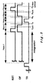
Figure 2 illustrates a timing diagram for signals at certain points within the readout circuit ofFigure 1 for an operational cycle having four phases; -
Figure 3 is similar toFigure 2 but illustrating an optional fifth phase; -
Figure 4 illustrates a noise-electron characteristic for the pixel photodiode readout circuit shown inFigure 1 where the capacitance of the overflow region is 10 times that of the floating diffusion region; -
Figure 5 illustrates a voltage-electron characteristic for the pixel photodiode readout circuit shown inFigure 1 ; -
Figure 6 illustrates noise-electron characteristics for elements of the pixel photodiode readout circuit shown inFigure 1 ; -
Figure 7 illustrates a signal-to-noise ratio-electron characteristic for the pixel photodiode readout circuit shown inFigure 1 ; -
Figure 8 is similar toFigure 6 but for a different offset capacitance value; and -
Figure 9 is similar toFigure 7 but for a different offset capacitance value. - The present disclosure will be described with respect to particular embodiments and with reference to certain drawings but the invention is not limited thereto. The drawings described are only schematic and are non-limiting. In the drawings, the size of some of the elements may be exaggerated and not drawn on scale for illustrative purposes.
- The terms "upper", "lower", "top", "bottom", "vertical" and "horizontal" as used herein refer to the orientation of the embodiments illustrated in drawings and is not intended to be limiting to a specific configuration.
- Referring initially to
Figure 1 , apixel circuit 100 is shown. It will be appreciated that each pixel within an image sensor will have such a circuit. - The
pixel circuit 100 comprises apixel photodiode 110 connected to anoutput 120 by means of a transfer (TX) gate orTX transistor 130, a floating diffusion (FD)region 140 and a readout gate orreadout transistor 150. TheFD region 140 is effectively implemented by anFD capacitor 145. Readout gate orreadout transistor 150 is connected to theoutput 120 as shown and to avoltage supply 155. A reset (RST) gate orRST transistor 160 is provided which is connected to anothervoltage supply 165 and to theFD region 140 via an overflow (OF) orcharge reservoir 170. In one embodiment, thevoltage supply 165 may be the same asvoltage supply 155 using the same physical interconnecting line in the pixel array (not shown). The OF orcharge reservoir 170 is effectively implemented by an OF gate or OFtransistor 180 and an OFcapacitor 190, as shown. Nodes A and B are shown between thepixel photodiode 110 andFD region 140, and between the RST gate orRST transistor 160 and the OF gate or OFtransistor 190 within the OF orcharge reservoir 170 respectively. The operation of thecircuit 100 will be described in more detail below with reference toFigures 2 and3 . - In effect, the
circuit 100 provides an additional reservoir, in the form of OFcapacitor 190 within the OF orcharge reservoir 170, for electrons when theFD region 140 becomes saturated. TheFD capacitor 145 has a smaller capacitance value than theOF capacitor 190, and hence, a higher conversion gain with low noise enabling a readout in a high-sensitivity mode. The overflowing electrons are transferred to theOF capacitor 190 where they are stored until theOF capacitor 190 is connected to theFD capacitor 145 to provide a lower conversion gain than that of theFD capacitor 145 alone as will be described in more detail below. This enables the readout of large signals after saturation of theFD capacitor 145. - A row select transistor (not shown) is provided for the selection of individual pixels for readout. However, this is not described in detail here as it is not relevant to the operation of the present invention.
- Referring now to
Figure 2 where a timing diagram is shown for the operation of thepixel circuit 100 with the signal levels for the TX gate orTX transistor 130, the RST gate orRST transistor 160 and the OF gate or OFtransistor 180. The signal levels are shown for four phases in each operational cycle of thepixel photodiode 110. -
Phase 1 relates to a signal integration phase, and, in a current frame, provides for the conversion of light incident on thepixel photodiode 110 into electrons. Here, all gates are set low as they are all open. Thepixel photodiode 110 integrates electrons that are generated by the light or photons detected in a standard 4T pixel operation. During readout of the previous frame, thepixel photodiode 110 is reset by closing TX gate ortransistor 130 during charge transfer to the FD region in that previous frame. With excessive incident light on thepixel photodiode 110, the operation of the RST gate ortransistor 160, the OF gate ortransistor 180 and the TX gate ortransistor 130 can be tuned to allow overflow once thepixel photodiode 110 is full as an "anti-blooming" measure, that is, the collection of an overflow of charge or electrons from the FD node connected to the pixel photodiode. - In
Phase 2, the OF gate ortransistor 170 and the RST gate ortransistor 160 are closed, that is, turned on, to set theFD region 140 to thesupply voltage 165. Subsequently, the RST gate ortransistor 160 is opened, that is, turned off. Optionally, at this point, an optional reset level of the combined capacitance of theFD capacitor 145 and theOF capacitor 190 can be sampled, readout via a pixel column output (not shown), and temporarily stored. The remainder of the charge on the combinedFD capacitor 145 and theOF capacitor 190 consists of some offset and noise due to sampling. The offset depends on thesupply voltage 165, the threshold voltage of the RST gate ortransistor 160, and the capacitive division of the parasitic capacitance of the RST gate ortransistor 160 with respect to the combined capacitance of theFD capacitor 145 and theOF capacitor 190. The larger the combined capacitance, the closer the reset level will be to the supply voltage. The reset level value, r A+B , can be expressed as:-
where OSA+B is the offset on the combined FD and overflow nodes, and
- The OF gate or
transistor 190 is then opened, that is, switched off, and a first reset level is sampled from theFD capacitor 145 only to the output. The offset depends on VA+B, the threshold voltage of the OF gate ortransistor 190, and the capacitive division of the parasitic capacitance of theOF capacitor 190 with respect to theFD capacitor 145. The larger the capacitance of theFD capacitor 145, the closer this reset level will be to VA+B. The reset noise level is approximately given by

where OSA is the offset on the FD node, and
- In
Phase 3, after sampling the reset level(s), rA (and r A+B if used), the TX gate or transistor is closed, that is, turned on, which empties the charge on thepixel photodiode 110 and aims to put all charge on theFD capacitor 145. If there is little charge, then a voltage gain will be produced:-
where QFD and CFD are the charge on and capacitance of respectively theFD capacitor 145. - If the charge is very large, node A will become very low making the OF gate or
transistor 190 conduct and allowing charge to overflow into and be stored in theOF capacitor 190. This overflow charge is not lost. A signal SA is measured at node A:-
where VCHARGE is the voltage due to the charge on thepixel photodiode 110. - By subtracting rA from SA , allowances can be made for the offset and the noise. If the result is low enough, that is, below a predetermined threshold, then the input signal from the
pixel photodiode 110 can be measured with high sensitivity and there is no need to use the OFregion 180. However, if the result is too large, some charge would have transferred to the OFregion 170 and the large signal on node B will need to be readout. - Clearly the OF gate or
transistor 180 needs to be specifically tuned to accommodate this mode of operation and to allow a certain charge overflow. The means that the 'OFF' state gate voltage needs to be different from 0V or that the OF gate orresistor 180 needs to be designed with a specific low threshold voltage. -
Phase 4 provides for the re-distribution of the total charge over theFD capacitor 145 and theOF capacitor 190. The OF gate ortransistor 190 is closed, that is, made to conduct, and the total charge is distributed over both capacitors. The total larger capacitance results in more charge capacity but at a lower sensitivity. For this signal, S A+B :-
where VCHARGE_TOTAL is the voltage due to the shared total charge from thepixel photodiode 110. - It is to be noted that the offset values OSA and OSA+B are different voltages which are due to the difference in capacitive action of the RST and OF gates or transistors. These values also contain fixed pattern noise (FPN) information for the
pixel photodiode 110 identifying a temporally constant lateral non-uniformity for the imaging system of which the pixel photodiode forms a part. - Similarly, the reset noise levels


- Nevertheless, in case the

- Alternatively, the reset level from the high gain measurement could be used to perform a pseudo correlated double sampling (CDS) operation in the voltage domain before gain compensation, that is, S A+ B - rA . This operation removes low frequency noise as well as the reset and source follower (SF) induced FPN, but keeps reset noise with overflow induced FPN and offset.
- As shown in
Figure 3 , the timing diagram includes anoptional Phase 5 in which a new reset value is sampled. Here, nodes A and B are reset again and measured, the new or further reset value, r A+ Bbis, is given by: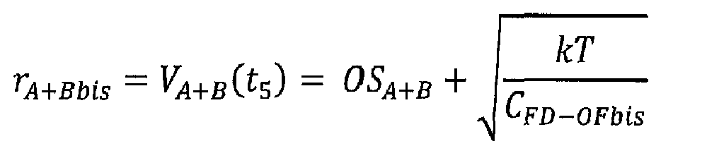
where OS A+B corresponds to the offset and FPN as before and
- The reset noise is now uncorrelated to the signal and will not be cancelled, but offset and FPN are cancelled. In other words, double data sampling (DDS) is performed for the low gain channel.
- The signal can then be defined as SA+B - r A+Bbis which corresponds to the lower sensitivity full signal including twice the reset noise. In most cases, this will be an acceptable and preferred operation mode. In this case, the original reset value will not need to be stored.
- If the maximum charge is 100000 electrons (e-), CFD = 1fF and COF = 10fF, then:
- At 10000e-, the voltage on the
FD capacitor 145 would be 1.6V (using

- Therefore, in order to obtain 1e- of noise, one needs to have readout circuits of 160µV, and above 10000e-, the charge needs to overflow into the overflow capacitor.
- With a COF = 10fF, at 100000e-, the voltage on the
OF capacitor 190 would be 1.6V (where QOF = 1.6 * 10-19 * 100000e-C and COF = 10fF). In this case, the maximum readable charge is 100000e- and the sensitivity is 16µV/e-. Here, in order to obtain 1e- of noise, one needs to have readout circuits of 16µV. This is far more difficult to achieve. However, as the signal is very large, the signal is also very noisy due to shot noise (shot noise in electrons being equal to the square root of the signal). -
Figure 4 illustrates a noise-input signal characteristic 400 for an input signal in electrons. The shot noise is indicated at 410 and read noise is indicated at 420, assuming a readout noise of 160µV under the above conditions. As can be seen, the shot noise is always greater than the readout noise. -
Figure 5 illustrates a voltage-input signal characteristic 500 for a pixel photodiode in terms of an input signal in electrons. The characteristic 500 includes the relationship between the voltage on the pixel photodiode and the charge it generates as shown at 510. A peak is shown at 520 which corresponds to a charge of 10000e- as given in the Example above and the end of the high sensitivity readout. A corresponding trough is shown at 530 which relates to a charge of more than 10000e- (again as given in the Example above) and which indicates the start of the readout at a lower sensitivity. The peak at 520 corresponds to the maximum charge sustained by theFD capacitor 145 and the trough at 530 corresponds to the transfer of charge to theOF capacitor 190. This results in lower sensitivity for larger signals, which is acceptable due to the shot noise (as described above with reference toFigure 4 . -
Figure 6 illustrates a noise-input signal characteristic 600 for operation at high sensitivity, that is, up to 10000e- as given in the Example above. InFigure 6 ,line 610 corresponds to shot noise;line 620 corresponds to the read noise;line 630 corresponds to the reset noise; line 640 (dotted line) corresponds to total noise for CDS at high gain;line 650 corresponds to total noise with no CDS; and line 660 (dotted line) corresponds to total noise using full CDS (indistinguishable fromline 640 for the used set of parameters). -
Figure 7 illustrates a signal-to-noise ratio (SNR)-input signal characteristic 700 for operation at the high sensitivity, that is, up to 10000e-. InFigure 7 ,line 710 corresponds to an ideal SNR;line 720 corresponds to SNR with no CDS; line 730 (darker dotted line) corresponds to CDS only at high gain; line 740 (solid line) corresponds to full CDS; and line 750 (lighter dotted line) corresponds to CDS only at high gain with DDS at low gain. -
Figure 8 is similar toFigure 6 whereline 810 corresponds to shot noise;line 820 corresponds to the read noise;line 830 corresponds to the reset noise; line 840 (lighter dotted line) corresponds to total noise for CDS at high gain;line 850 corresponds to total noise with no CDS; and line 860 (dotted line) corresponds to total noise using full CDS (at lowest signal levels line 840 masks line 860). -
Figure 9 is similar toFigure 7 whereline 910 corresponds to an ideal SNR;line 920 corresponds to SNR with no CDS; line 930 (lighter dotted line) corresponds to CDS only at high gain; line 940 (darker dotted line) corresponds to full CDS; and line 950 (solid line) corresponds to CDS only at high gain with DDS at low gain. A small dip is observed at the point where the gain channel is changed from a high sensitivity to a lower sensitivity. - The SNR dip can vary, for example, in the case of a swing of 1V and capacitance values of 1fF and 40fF, the SNR dip can be between 1 to 5dB depending on the handling of the reset level.
- The operation of the circuit of the present invention has the advantage that a higher dynamic range can be provided with the additional cost of one additional transistor and capacitor for each pixel photodiode in a photodiode array.
- Two readout channels are provided when the charge is at a level where the FD capacitor becomes saturated, each channel having a different sensitivity. Both channels share the same amplifier path making FPN subtraction easier to process.
- Offset and reset noise cancellation can be provided for in a reset sample subtraction process.
- Using the circuit of the present invention, performing CDS in combination with 1/f noise cancellation is possible.
- FD sharing is possible which allows the sharing of all pixel circuitry with the exception of the TX gate or transistor and the pixel photodiode itself.
- Pixel binning may be provided to increase further the dynamic range with an associated trade-off with loss in resolution.
- The invention of the present disclosure has the advantage that "anti-blooming" functionality is provided without loss of sensitivity and without having to know beforehand the amount of "blooming" or overflow which will be needed. When overflow is needed, extra information is provided about the incoming light signal with increased dynamic range.
- Such a
pixel photodiode circuit 100 may be utilised in any image sensor to produce the advantages mentioned above. - Although the present disclosure has been described with reference to a 4T pixel arrangement, it can also be used with a 3T pixel arrangement where the transfer gate is removed.
- It will readily be appreciated that although the concept has been explained for electrons as signal carriers and NMOS transistors, equivalently holes as signal carriers and PMOS transistors could be used as well driven in the appropriate way.
- It will readily be appreciated that although one specific embodiment has been described, other implementations are also possible.
Claims (9)
- A method of obtaining an output signal from a pixel photodiode (110) which includes floating diffusion region (140) and an overflow diffusion region (170), the method comprising the steps of:-a) transferring electrons from the pixel photodiode (110) to the floating diffusion region (140);b) receiving electrons in the floating diffusion region (140) from the pixel photodiode (110) and converting the received electrons into at least one charge value corresponding to the received electrons in the floating diffusion region (140) to provide at least one output signal; andc) reading out said at least one output signal;characterised in that step b) further comprises the steps of:-b1) transferring electrons from the floating diffusion region (140) to the overflow diffusion region (170);b2) reading out a first output signal (SA ), corresponding to a first charge value, from the floating diffusion region (140) at a first sensitivity level;b3) converting the received electrons in the overflow region (170) into a second charge value;b4) re-distributing the first and second charge values over both the floating diffusion region (140) and the overflow diffusion region (170);b5) converting said re-distributed charge on the combined floating diffusion and overflow diffusion regions (140, 170) into a second output signal (S A+B ); andb6) reading out the second output signal (S A+B ), corresponding to said redistributed charge value, from the floating diffusion region (140) at a second sensitivity level, the second sensitivity level being lower than the first sensitivity level.
- A method according to claim 1, further comprising, prior to step a), the step of integrating the electrons accumulated on the pixel photodiode (110).
- A method according to claim 1 or 2, wherein step b) further comprises the step of:-b1a) sampling a first reset level value (rA ) for the first output signal prior to step b2).
- A method according to claim 3, wherein step b2) comprises using the first reset level value (rA ) to compensate for at least one of: noise and offset in the first output signal (SA ).
- A method according to claim 3 or 4, wherein step b) further comprises the step of sampling an optional reset level value (r A+B ) prior to step b1a).
- A method according to claim 5, wherein step b6) comprises using the optional reset level value (r A+B ) to compensate for at least one of: noise and offset in the second output signal (S A+B ).
- A method according to any one of the preceding claims, further comprising the step of sampling a further reset level value (r A+Bbis ) prior to step b6).
- A method according to claim 7, further comprising the step of using the further reset level value (rA+Bbis ) to compensate for at least one of: offset and fixed pattern noise.
- A method according to claim 5 or 6, further comprising the step of storing the optional reset level value (r A+B ).
Priority Applications (2)
| Application Number | Priority Date | Filing Date | Title |
|---|---|---|---|
| EP13199615.9A EP2890117B1 (en) | 2013-12-26 | 2013-12-26 | Improvements in or relating to imaging sensors |
| US14/574,383 US9313428B2 (en) | 2013-12-26 | 2014-12-17 | Imaging sensors |
Applications Claiming Priority (1)
| Application Number | Priority Date | Filing Date | Title |
|---|---|---|---|
| EP13199615.9A EP2890117B1 (en) | 2013-12-26 | 2013-12-26 | Improvements in or relating to imaging sensors |
Publications (2)
| Publication Number | Publication Date |
|---|---|
| EP2890117A1 true EP2890117A1 (en) | 2015-07-01 |
| EP2890117B1 EP2890117B1 (en) | 2020-11-18 |
Family
ID=49841601
Family Applications (1)
| Application Number | Title | Priority Date | Filing Date |
|---|---|---|---|
| EP13199615.9A Active EP2890117B1 (en) | 2013-12-26 | 2013-12-26 | Improvements in or relating to imaging sensors |
Country Status (2)
| Country | Link |
|---|---|
| US (1) | US9313428B2 (en) |
| EP (1) | EP2890117B1 (en) |
Cited By (3)
| Publication number | Priority date | Publication date | Assignee | Title |
|---|---|---|---|---|
| US9756270B2 (en) | 2014-12-16 | 2017-09-05 | Imec Vzw | In-pixel amplification device and method |
| WO2019096420A1 (en) | 2017-11-20 | 2019-05-23 | Ecole Polytechnique Fédérale De Lausanne Epfl-Tto | Pixel sensor cell for cmos image sensors with enhanced conversion gain at high dynamic range capability |
| EP4270979A1 (en) * | 2022-04-28 | 2023-11-01 | Brillnics Singapore Pte. Ltd. | Solid-state imaging device, method for driving solid-state imaging device, and electronic apparatus |
Families Citing this family (13)
| Publication number | Priority date | Publication date | Assignee | Title |
|---|---|---|---|---|
| US9686490B2 (en) * | 2014-04-01 | 2017-06-20 | Sensors Unlimited, Inc. | Integrating pixels and methods of operation |
| US9706142B2 (en) | 2015-09-23 | 2017-07-11 | Semiconductor Components Industries, Llc | High dynamic range and global shutter image sensor pixels having charge overflow signal detecting structures |
| US9900481B2 (en) * | 2015-11-25 | 2018-02-20 | Semiconductor Components Industries, Llc | Imaging pixels having coupled gate structure |
| EP3378099A4 (en) | 2016-01-15 | 2019-08-28 | Invisage Technologies, Inc. | IMAGE SENSORS COMPRISING A GLOBAL ELECTRONIC SHUTTER |
| US10250826B2 (en) | 2016-01-15 | 2019-04-02 | Invisage Technologies, Inc. | Image sensors having extended dynamic range |
| US10072974B2 (en) * | 2016-06-06 | 2018-09-11 | Semiconductor Components Industries, Llc | Image sensors with LED flicker mitigaton global shutter pixles |
| US10341571B2 (en) | 2016-06-08 | 2019-07-02 | Invisage Technologies, Inc. | Image sensors with electronic shutter |
| FR3062519B1 (en) * | 2017-01-31 | 2019-03-29 | Stmicroelectronics (Crolles 2) Sas | IMAGE SENSOR WITH LARGE DYNAMIC AND LOW NOISE RANGE |
| US10103193B1 (en) * | 2017-08-03 | 2018-10-16 | Omnivision Technologies, Inc. | Apparatus and method for low dark current floating diffusion |
| US11064141B2 (en) * | 2019-07-24 | 2021-07-13 | Semiconductor Components Industries, Llc | Imaging systems and methods for reducing dark signal non-uniformity across pixels |
| KR20220165006A (en) | 2021-06-07 | 2022-12-14 | 삼성전자주식회사 | Image sensor including pixel including internal capacitor |
| KR20240011499A (en) * | 2022-07-19 | 2024-01-26 | 에스케이하이닉스 주식회사 | Image Sensing Device and Imaging Device including the same |
| CN119854665B (en) * | 2024-06-12 | 2026-05-29 | 比亚迪半导体股份有限公司 | Pixel circuit, image sensor and camera |
Citations (2)
| Publication number | Priority date | Publication date | Assignee | Title |
|---|---|---|---|---|
| US20120256077A1 (en) * | 2011-04-08 | 2012-10-11 | PixArt Imaging Incorporation, R.O.C. | High dynamic range imager circuit and method for reading high dynamic range image |
| US20130194472A1 (en) * | 2012-02-01 | 2013-08-01 | Sony Corporation | Solid-state imaging device, driving method and electronic device |
Family Cites Families (5)
| Publication number | Priority date | Publication date | Assignee | Title |
|---|---|---|---|---|
| US7091531B2 (en) | 2004-04-07 | 2006-08-15 | Micron Technology, Inc. | High dynamic range pixel amplifier |
| EP2190185B1 (en) | 2007-09-05 | 2013-11-06 | Tohoku University | Solid-state image sensor |
| CN102057671B (en) * | 2008-06-10 | 2013-03-13 | 国立大学法人东北大学 | Solid-state imaging device and driving method for same |
| GB2487740A (en) | 2011-02-01 | 2012-08-08 | Cmosis Nv | High Dynamic Range Pixel Structure |
| TWI533699B (en) * | 2012-01-27 | 2016-05-11 | Sony Corp | A solid-state imaging element and a driving method, and an electronic device |
-
2013
- 2013-12-26 EP EP13199615.9A patent/EP2890117B1/en active Active
-
2014
- 2014-12-17 US US14/574,383 patent/US9313428B2/en active Active
Patent Citations (2)
| Publication number | Priority date | Publication date | Assignee | Title |
|---|---|---|---|---|
| US20120256077A1 (en) * | 2011-04-08 | 2012-10-11 | PixArt Imaging Incorporation, R.O.C. | High dynamic range imager circuit and method for reading high dynamic range image |
| US20130194472A1 (en) * | 2012-02-01 | 2013-08-01 | Sony Corporation | Solid-state imaging device, driving method and electronic device |
Non-Patent Citations (2)
| Title |
|---|
| JAEHYUK CHOI: "An Energy-efficient Adaptive CMOS Image Sensor", 12 June 2013 (2013-06-12), The University of Michigan, pages FP - 158, XP002719154, Retrieved from the Internet <URL:http://deepblue.lib.umich.edu/bitstream/handle/2027.42/97883/jaechoi_1.pdf?sequence=1> [retrieved on 20140121] * |
| XINYANG WANG ET AL: "Paper number: R36 An 89dB Dynamic Range CMOS Image Sensor with Dual Transfer Gate Pixel", 31 December 2011 (2011-12-31), XP055097725, Retrieved from the Internet <URL:http://www.imagesensors.org/Past Workshops/2011 Workshop/2011 Papers/R36_Wang_DualTG.pdf> [retrieved on 20140122] * |
Cited By (5)
| Publication number | Priority date | Publication date | Assignee | Title |
|---|---|---|---|---|
| US9756270B2 (en) | 2014-12-16 | 2017-09-05 | Imec Vzw | In-pixel amplification device and method |
| WO2019096420A1 (en) | 2017-11-20 | 2019-05-23 | Ecole Polytechnique Fédérale De Lausanne Epfl-Tto | Pixel sensor cell for cmos image sensors with enhanced conversion gain at high dynamic range capability |
| US11252352B2 (en) | 2017-11-20 | 2022-02-15 | Ecole polytechnique fédérale de Lausanne (EPFL) | Pixel sensor cell for CMOS image sensors with enhanced conversion gain at high dynamic range capability |
| EP4270979A1 (en) * | 2022-04-28 | 2023-11-01 | Brillnics Singapore Pte. Ltd. | Solid-state imaging device, method for driving solid-state imaging device, and electronic apparatus |
| US12294793B2 (en) | 2022-04-28 | 2025-05-06 | Brillnics Singapore Pte. Ltd. | Solid-state imaging device, method for driving solid-state imaging device, and electronic apparatus |
Also Published As
| Publication number | Publication date |
|---|---|
| US9313428B2 (en) | 2016-04-12 |
| EP2890117B1 (en) | 2020-11-18 |
| US20150189199A1 (en) | 2015-07-02 |
Similar Documents
| Publication | Publication Date | Title |
|---|---|---|
| EP2890117B1 (en) | Improvements in or relating to imaging sensors | |
| US11765474B2 (en) | Pixel arrangement, image sensor and method of operating a pixel arrangement | |
| US8089036B2 (en) | Image sensor with global shutter and in pixel storage transistor | |
| US9432597B2 (en) | Low-noise, high dynamic-range image sensor | |
| JP4374115B2 (en) | Active pixel sensor | |
| US10560646B2 (en) | Global-shutter vertically integrated pixel with high dynamic range | |
| US7205522B2 (en) | Pixel circuit for image sensor | |
| CN107852473B (en) | Method for controlling an active pixel image sensor | |
| US8569671B2 (en) | Pixel array capable of performing pipelined global shutter operation including a first and second buffer amplifier | |
| US8217328B2 (en) | Low noise pixel readout circuit with high conversion gain | |
| US9172851B2 (en) | CMOS linear image sensor with motion-blur compensation | |
| US10200644B2 (en) | Global shutter scheme that reduces the effects of dark current | |
| US20080246869A1 (en) | Differential readout from pixels in CMOS sensor | |
| JP4288346B2 (en) | Imaging device and pixel circuit | |
| US20070152137A1 (en) | Differential column readout scheme for CMOS APS pixels | |
| WO2009055255A1 (en) | Methods, systems and apparatuses using barrier self-calibration for high dynamic range imagers | |
| CN110233978A (en) | Feedthrough compensates imaging sensor | |
| US20100079632A1 (en) | Correlated double sampling pixel | |
| KR20120112778A (en) | Solid-state image pickup device, method of reading pixel signal, and pixel | |
| US20090321799A1 (en) | Method and apparatus for increasing conversion gain in imagers | |
| US9843757B2 (en) | Optical electronic device including enhanced global shutter pixel array and related methods | |
| US9998693B2 (en) | Image sensor adapted to blinking sources | |
| KR101241466B1 (en) | Pixel arrary, image sensor including the same and a method of driving the same | |
| US20150076321A1 (en) | Amplifier Adapted for CMOS Imaging Sensors | |
| US9143712B2 (en) | Solid state imaging device, driving method of solid state imaging device, and electronic device having a driving unit so that a potential of a drain of a charge reset unit is controlled |
Legal Events
| Date | Code | Title | Description |
|---|---|---|---|
| PUAI | Public reference made under article 153(3) epc to a published international application that has entered the european phase |
Free format text: ORIGINAL CODE: 0009012 |
|
| 17P | Request for examination filed |
Effective date: 20131226 |
|
| AK | Designated contracting states |
Kind code of ref document: A1 Designated state(s): AL AT BE BG CH CY CZ DE DK EE ES FI FR GB GR HR HU IE IS IT LI LT LU LV MC MK MT NL NO PL PT RO RS SE SI SK SM TR |
|
| AX | Request for extension of the european patent |
Extension state: BA ME |
|
| R17P | Request for examination filed (corrected) |
Effective date: 20160104 |
|
| RBV | Designated contracting states (corrected) |
Designated state(s): AL AT BE BG CH CY CZ DE DK EE ES FI FR GB GR HR HU IE IS IT LI LT LU LV MC MK MT NL NO PL PT RO RS SE SI SK SM TR |
|
| 17Q | First examination report despatched |
Effective date: 20160603 |
|
| STAA | Information on the status of an ep patent application or granted ep patent |
Free format text: STATUS: EXAMINATION IS IN PROGRESS |
|
| GRAP | Despatch of communication of intention to grant a patent |
Free format text: ORIGINAL CODE: EPIDOSNIGR1 |
|
| STAA | Information on the status of an ep patent application or granted ep patent |
Free format text: STATUS: GRANT OF PATENT IS INTENDED |
|
| INTG | Intention to grant announced |
Effective date: 20200608 |
|
| GRAS | Grant fee paid |
Free format text: ORIGINAL CODE: EPIDOSNIGR3 |
|
| GRAA | (expected) grant |
Free format text: ORIGINAL CODE: 0009210 |
|
| STAA | Information on the status of an ep patent application or granted ep patent |
Free format text: STATUS: THE PATENT HAS BEEN GRANTED |
|
| AK | Designated contracting states |
Kind code of ref document: B1 Designated state(s): AL AT BE BG CH CY CZ DE DK EE ES FI FR GB GR HR HU IE IS IT LI LT LU LV MC MK MT NL NO PL PT RO RS SE SI SK SM TR |
|
| REG | Reference to a national code |
Ref country code: GB Ref legal event code: FG4D |
|
| REG | Reference to a national code |
Ref country code: CH Ref legal event code: EP |
|
| REG | Reference to a national code |
Ref country code: DE Ref legal event code: R096 Ref document number: 602013074098 Country of ref document: DE |
|
| REG | Reference to a national code |
Ref country code: IE Ref legal event code: FG4D |
|
| REG | Reference to a national code |
Ref country code: AT Ref legal event code: REF Ref document number: 1337016 Country of ref document: AT Kind code of ref document: T Effective date: 20201215 |
|
| REG | Reference to a national code |
Ref country code: AT Ref legal event code: MK05 Ref document number: 1337016 Country of ref document: AT Kind code of ref document: T Effective date: 20201118 |
|
| REG | Reference to a national code |
Ref country code: NL Ref legal event code: MP Effective date: 20201118 |
|
| PG25 | Lapsed in a contracting state [announced via postgrant information from national office to epo] |
Ref country code: PT Free format text: LAPSE BECAUSE OF FAILURE TO SUBMIT A TRANSLATION OF THE DESCRIPTION OR TO PAY THE FEE WITHIN THE PRESCRIBED TIME-LIMIT Effective date: 20210318 Ref country code: NO Free format text: LAPSE BECAUSE OF FAILURE TO SUBMIT A TRANSLATION OF THE DESCRIPTION OR TO PAY THE FEE WITHIN THE PRESCRIBED TIME-LIMIT Effective date: 20210218 Ref country code: FI Free format text: LAPSE BECAUSE OF FAILURE TO SUBMIT A TRANSLATION OF THE DESCRIPTION OR TO PAY THE FEE WITHIN THE PRESCRIBED TIME-LIMIT Effective date: 20201118 Ref country code: RS Free format text: LAPSE BECAUSE OF FAILURE TO SUBMIT A TRANSLATION OF THE DESCRIPTION OR TO PAY THE FEE WITHIN THE PRESCRIBED TIME-LIMIT Effective date: 20201118 Ref country code: GR Free format text: LAPSE BECAUSE OF FAILURE TO SUBMIT A TRANSLATION OF THE DESCRIPTION OR TO PAY THE FEE WITHIN THE PRESCRIBED TIME-LIMIT Effective date: 20210219 |
|
| PG25 | Lapsed in a contracting state [announced via postgrant information from national office to epo] |
Ref country code: BG Free format text: LAPSE BECAUSE OF FAILURE TO SUBMIT A TRANSLATION OF THE DESCRIPTION OR TO PAY THE FEE WITHIN THE PRESCRIBED TIME-LIMIT Effective date: 20210218 Ref country code: AT Free format text: LAPSE BECAUSE OF FAILURE TO SUBMIT A TRANSLATION OF THE DESCRIPTION OR TO PAY THE FEE WITHIN THE PRESCRIBED TIME-LIMIT Effective date: 20201118 Ref country code: PL Free format text: LAPSE BECAUSE OF FAILURE TO SUBMIT A TRANSLATION OF THE DESCRIPTION OR TO PAY THE FEE WITHIN THE PRESCRIBED TIME-LIMIT Effective date: 20201118 Ref country code: LV Free format text: LAPSE BECAUSE OF FAILURE TO SUBMIT A TRANSLATION OF THE DESCRIPTION OR TO PAY THE FEE WITHIN THE PRESCRIBED TIME-LIMIT Effective date: 20201118 Ref country code: SE Free format text: LAPSE BECAUSE OF FAILURE TO SUBMIT A TRANSLATION OF THE DESCRIPTION OR TO PAY THE FEE WITHIN THE PRESCRIBED TIME-LIMIT Effective date: 20201118 Ref country code: IS Free format text: LAPSE BECAUSE OF FAILURE TO SUBMIT A TRANSLATION OF THE DESCRIPTION OR TO PAY THE FEE WITHIN THE PRESCRIBED TIME-LIMIT Effective date: 20210318 |
|
| REG | Reference to a national code |
Ref country code: LT Ref legal event code: MG9D |
|
| PG25 | Lapsed in a contracting state [announced via postgrant information from national office to epo] |
Ref country code: HR Free format text: LAPSE BECAUSE OF FAILURE TO SUBMIT A TRANSLATION OF THE DESCRIPTION OR TO PAY THE FEE WITHIN THE PRESCRIBED TIME-LIMIT Effective date: 20201118 |
|
| PG25 | Lapsed in a contracting state [announced via postgrant information from national office to epo] |
Ref country code: RO Free format text: LAPSE BECAUSE OF FAILURE TO SUBMIT A TRANSLATION OF THE DESCRIPTION OR TO PAY THE FEE WITHIN THE PRESCRIBED TIME-LIMIT Effective date: 20201118 Ref country code: SK Free format text: LAPSE BECAUSE OF FAILURE TO SUBMIT A TRANSLATION OF THE DESCRIPTION OR TO PAY THE FEE WITHIN THE PRESCRIBED TIME-LIMIT Effective date: 20201118 Ref country code: LT Free format text: LAPSE BECAUSE OF FAILURE TO SUBMIT A TRANSLATION OF THE DESCRIPTION OR TO PAY THE FEE WITHIN THE PRESCRIBED TIME-LIMIT Effective date: 20201118 Ref country code: SM Free format text: LAPSE BECAUSE OF FAILURE TO SUBMIT A TRANSLATION OF THE DESCRIPTION OR TO PAY THE FEE WITHIN THE PRESCRIBED TIME-LIMIT Effective date: 20201118 Ref country code: CZ Free format text: LAPSE BECAUSE OF FAILURE TO SUBMIT A TRANSLATION OF THE DESCRIPTION OR TO PAY THE FEE WITHIN THE PRESCRIBED TIME-LIMIT Effective date: 20201118 Ref country code: EE Free format text: LAPSE BECAUSE OF FAILURE TO SUBMIT A TRANSLATION OF THE DESCRIPTION OR TO PAY THE FEE WITHIN THE PRESCRIBED TIME-LIMIT Effective date: 20201118 |
|
| REG | Reference to a national code |
Ref country code: CH Ref legal event code: PL |
|
| REG | Reference to a national code |
Ref country code: DE Ref legal event code: R097 Ref document number: 602013074098 Country of ref document: DE |
|
| PG25 | Lapsed in a contracting state [announced via postgrant information from national office to epo] |
Ref country code: DK Free format text: LAPSE BECAUSE OF FAILURE TO SUBMIT A TRANSLATION OF THE DESCRIPTION OR TO PAY THE FEE WITHIN THE PRESCRIBED TIME-LIMIT Effective date: 20201118 Ref country code: MC Free format text: LAPSE BECAUSE OF FAILURE TO SUBMIT A TRANSLATION OF THE DESCRIPTION OR TO PAY THE FEE WITHIN THE PRESCRIBED TIME-LIMIT Effective date: 20201118 |
|
| REG | Reference to a national code |
Ref country code: BE Ref legal event code: MM Effective date: 20201231 |
|
| PLBE | No opposition filed within time limit |
Free format text: ORIGINAL CODE: 0009261 |
|
| STAA | Information on the status of an ep patent application or granted ep patent |
Free format text: STATUS: NO OPPOSITION FILED WITHIN TIME LIMIT |
|
| 26N | No opposition filed |
Effective date: 20210819 |
|
| GBPC | Gb: european patent ceased through non-payment of renewal fee |
Effective date: 20210218 |
|
| PG25 | Lapsed in a contracting state [announced via postgrant information from national office to epo] |
Ref country code: LU Free format text: LAPSE BECAUSE OF NON-PAYMENT OF DUE FEES Effective date: 20201226 Ref country code: NL Free format text: LAPSE BECAUSE OF FAILURE TO SUBMIT A TRANSLATION OF THE DESCRIPTION OR TO PAY THE FEE WITHIN THE PRESCRIBED TIME-LIMIT Effective date: 20201118 Ref country code: AL Free format text: LAPSE BECAUSE OF FAILURE TO SUBMIT A TRANSLATION OF THE DESCRIPTION OR TO PAY THE FEE WITHIN THE PRESCRIBED TIME-LIMIT Effective date: 20201118 Ref country code: IE Free format text: LAPSE BECAUSE OF NON-PAYMENT OF DUE FEES Effective date: 20201226 Ref country code: IT Free format text: LAPSE BECAUSE OF FAILURE TO SUBMIT A TRANSLATION OF THE DESCRIPTION OR TO PAY THE FEE WITHIN THE PRESCRIBED TIME-LIMIT Effective date: 20201118 |
|
| PG25 | Lapsed in a contracting state [announced via postgrant information from national office to epo] |
Ref country code: SI Free format text: LAPSE BECAUSE OF FAILURE TO SUBMIT A TRANSLATION OF THE DESCRIPTION OR TO PAY THE FEE WITHIN THE PRESCRIBED TIME-LIMIT Effective date: 20201118 Ref country code: LI Free format text: LAPSE BECAUSE OF NON-PAYMENT OF DUE FEES Effective date: 20201231 Ref country code: CH Free format text: LAPSE BECAUSE OF NON-PAYMENT OF DUE FEES Effective date: 20201231 Ref country code: ES Free format text: LAPSE BECAUSE OF FAILURE TO SUBMIT A TRANSLATION OF THE DESCRIPTION OR TO PAY THE FEE WITHIN THE PRESCRIBED TIME-LIMIT Effective date: 20201118 |
|
| PG25 | Lapsed in a contracting state [announced via postgrant information from national office to epo] |
Ref country code: GB Free format text: LAPSE BECAUSE OF NON-PAYMENT OF DUE FEES Effective date: 20210218 |
|
| PG25 | Lapsed in a contracting state [announced via postgrant information from national office to epo] |
Ref country code: IS Free format text: LAPSE BECAUSE OF FAILURE TO SUBMIT A TRANSLATION OF THE DESCRIPTION OR TO PAY THE FEE WITHIN THE PRESCRIBED TIME-LIMIT Effective date: 20210318 Ref country code: TR Free format text: LAPSE BECAUSE OF FAILURE TO SUBMIT A TRANSLATION OF THE DESCRIPTION OR TO PAY THE FEE WITHIN THE PRESCRIBED TIME-LIMIT Effective date: 20201118 Ref country code: MT Free format text: LAPSE BECAUSE OF FAILURE TO SUBMIT A TRANSLATION OF THE DESCRIPTION OR TO PAY THE FEE WITHIN THE PRESCRIBED TIME-LIMIT Effective date: 20201118 Ref country code: CY Free format text: LAPSE BECAUSE OF FAILURE TO SUBMIT A TRANSLATION OF THE DESCRIPTION OR TO PAY THE FEE WITHIN THE PRESCRIBED TIME-LIMIT Effective date: 20201118 |
|
| PG25 | Lapsed in a contracting state [announced via postgrant information from national office to epo] |
Ref country code: MK Free format text: LAPSE BECAUSE OF FAILURE TO SUBMIT A TRANSLATION OF THE DESCRIPTION OR TO PAY THE FEE WITHIN THE PRESCRIBED TIME-LIMIT Effective date: 20201118 |
|
| PG25 | Lapsed in a contracting state [announced via postgrant information from national office to epo] |
Ref country code: BE Free format text: LAPSE BECAUSE OF NON-PAYMENT OF DUE FEES Effective date: 20201231 |
|
| REG | Reference to a national code |
Ref country code: DE Ref legal event code: R079 Ref document number: 602013074098 Country of ref document: DE Free format text: PREVIOUS MAIN CLASS: H04N0005355000 Ipc: H04N0025570000 |
|
| P01 | Opt-out of the competence of the unified patent court (upc) registered |
Effective date: 20230513 |
|
| PGFP | Annual fee paid to national office [announced via postgrant information from national office to epo] |
Ref country code: DE Payment date: 20251126 Year of fee payment: 13 |
|
| PGFP | Annual fee paid to national office [announced via postgrant information from national office to epo] |
Ref country code: FR Payment date: 20251120 Year of fee payment: 13 |