EP2889918B1 - Preparation method of solar cell with stainless steel substrate of adjustable bandgap quantum well structure - Google Patents
Preparation method of solar cell with stainless steel substrate of adjustable bandgap quantum well structure Download PDFInfo
- Publication number
- EP2889918B1 EP2889918B1 EP14162221.7A EP14162221A EP2889918B1 EP 2889918 B1 EP2889918 B1 EP 2889918B1 EP 14162221 A EP14162221 A EP 14162221A EP 2889918 B1 EP2889918 B1 EP 2889918B1
- Authority
- EP
- European Patent Office
- Prior art keywords
- type
- film
- gzo
- deposition
- stainless steel
- Prior art date
- Legal status (The legal status is an assumption and is not a legal conclusion. Google has not performed a legal analysis and makes no representation as to the accuracy of the status listed.)
- Not-in-force
Links
Images




Classifications
-
- H—ELECTRICITY
- H10—SEMICONDUCTOR DEVICES; ELECTRIC SOLID-STATE DEVICES NOT OTHERWISE PROVIDED FOR
- H10F—INORGANIC SEMICONDUCTOR DEVICES SENSITIVE TO INFRARED RADIATION, LIGHT, ELECTROMAGNETIC RADIATION OF SHORTER WAVELENGTH OR CORPUSCULAR RADIATION
- H10F77/00—Constructional details of devices covered by this subclass
- H10F77/10—Semiconductor bodies
- H10F77/12—Active materials
- H10F77/124—Active materials comprising only Group III-V materials, e.g. GaAs
- H10F77/1248—Active materials comprising only Group III-V materials, e.g. GaAs having three or more elements, e.g. GaAlAs, InGaAs or InGaAsP
- H10F77/12485—Active materials comprising only Group III-V materials, e.g. GaAs having three or more elements, e.g. GaAlAs, InGaAs or InGaAsP comprising nitride compounds, e.g. InGaN
-
- H—ELECTRICITY
- H10—SEMICONDUCTOR DEVICES; ELECTRIC SOLID-STATE DEVICES NOT OTHERWISE PROVIDED FOR
- H10F—INORGANIC SEMICONDUCTOR DEVICES SENSITIVE TO INFRARED RADIATION, LIGHT, ELECTROMAGNETIC RADIATION OF SHORTER WAVELENGTH OR CORPUSCULAR RADIATION
- H10F77/00—Constructional details of devices covered by this subclass
- H10F77/10—Semiconductor bodies
- H10F77/14—Shape of semiconductor bodies; Shapes, relative sizes or dispositions of semiconductor regions within semiconductor bodies
- H10F77/148—Shapes of potential barriers
-
- H—ELECTRICITY
- H10—SEMICONDUCTOR DEVICES; ELECTRIC SOLID-STATE DEVICES NOT OTHERWISE PROVIDED FOR
- H10F—INORGANIC SEMICONDUCTOR DEVICES SENSITIVE TO INFRARED RADIATION, LIGHT, ELECTROMAGNETIC RADIATION OF SHORTER WAVELENGTH OR CORPUSCULAR RADIATION
- H10F10/00—Individual photovoltaic cells, e.g. solar cells
- H10F10/10—Individual photovoltaic cells, e.g. solar cells having potential barriers
- H10F10/17—Photovoltaic cells having only PIN junction potential barriers
-
- H—ELECTRICITY
- H10—SEMICONDUCTOR DEVICES; ELECTRIC SOLID-STATE DEVICES NOT OTHERWISE PROVIDED FOR
- H10F—INORGANIC SEMICONDUCTOR DEVICES SENSITIVE TO INFRARED RADIATION, LIGHT, ELECTROMAGNETIC RADIATION OF SHORTER WAVELENGTH OR CORPUSCULAR RADIATION
- H10F71/00—Manufacture or treatment of devices covered by this subclass
- H10F71/10—Manufacture or treatment of devices covered by this subclass the devices comprising amorphous semiconductor material
-
- H—ELECTRICITY
- H10—SEMICONDUCTOR DEVICES; ELECTRIC SOLID-STATE DEVICES NOT OTHERWISE PROVIDED FOR
- H10F—INORGANIC SEMICONDUCTOR DEVICES SENSITIVE TO INFRARED RADIATION, LIGHT, ELECTROMAGNETIC RADIATION OF SHORTER WAVELENGTH OR CORPUSCULAR RADIATION
- H10F71/00—Manufacture or treatment of devices covered by this subclass
- H10F71/10—Manufacture or treatment of devices covered by this subclass the devices comprising amorphous semiconductor material
- H10F71/103—Manufacture or treatment of devices covered by this subclass the devices comprising amorphous semiconductor material including only Group IV materials
-
- H—ELECTRICITY
- H10—SEMICONDUCTOR DEVICES; ELECTRIC SOLID-STATE DEVICES NOT OTHERWISE PROVIDED FOR
- H10F—INORGANIC SEMICONDUCTOR DEVICES SENSITIVE TO INFRARED RADIATION, LIGHT, ELECTROMAGNETIC RADIATION OF SHORTER WAVELENGTH OR CORPUSCULAR RADIATION
- H10F71/00—Manufacture or treatment of devices covered by this subclass
- H10F71/127—The active layers comprising only Group III-V materials, e.g. GaAs or InP
- H10F71/1272—The active layers comprising only Group III-V materials, e.g. GaAs or InP comprising at least three elements, e.g. GaAlAs or InGaAsP
- H10F71/1274—The active layers comprising only Group III-V materials, e.g. GaAs or InP comprising at least three elements, e.g. GaAlAs or InGaAsP comprising nitrides, e.g. InGaN or InGaAlN
-
- H—ELECTRICITY
- H10—SEMICONDUCTOR DEVICES; ELECTRIC SOLID-STATE DEVICES NOT OTHERWISE PROVIDED FOR
- H10F—INORGANIC SEMICONDUCTOR DEVICES SENSITIVE TO INFRARED RADIATION, LIGHT, ELECTROMAGNETIC RADIATION OF SHORTER WAVELENGTH OR CORPUSCULAR RADIATION
- H10F77/00—Constructional details of devices covered by this subclass
- H10F77/10—Semiconductor bodies
- H10F77/14—Shape of semiconductor bodies; Shapes, relative sizes or dispositions of semiconductor regions within semiconductor bodies
- H10F77/143—Shape of semiconductor bodies; Shapes, relative sizes or dispositions of semiconductor regions within semiconductor bodies comprising quantum structures
-
- H—ELECTRICITY
- H10—SEMICONDUCTOR DEVICES; ELECTRIC SOLID-STATE DEVICES NOT OTHERWISE PROVIDED FOR
- H10F—INORGANIC SEMICONDUCTOR DEVICES SENSITIVE TO INFRARED RADIATION, LIGHT, ELECTROMAGNETIC RADIATION OF SHORTER WAVELENGTH OR CORPUSCULAR RADIATION
- H10F77/00—Constructional details of devices covered by this subclass
- H10F77/10—Semiconductor bodies
- H10F77/14—Shape of semiconductor bodies; Shapes, relative sizes or dispositions of semiconductor regions within semiconductor bodies
- H10F77/146—Superlattices; Multiple quantum well structures
-
- H—ELECTRICITY
- H10—SEMICONDUCTOR DEVICES; ELECTRIC SOLID-STATE DEVICES NOT OTHERWISE PROVIDED FOR
- H10F—INORGANIC SEMICONDUCTOR DEVICES SENSITIVE TO INFRARED RADIATION, LIGHT, ELECTROMAGNETIC RADIATION OF SHORTER WAVELENGTH OR CORPUSCULAR RADIATION
- H10F77/00—Constructional details of devices covered by this subclass
- H10F77/10—Semiconductor bodies
- H10F77/16—Material structures, e.g. crystalline structures, film structures or crystal plane orientations
- H10F77/162—Non-monocrystalline materials, e.g. semiconductor particles embedded in insulating materials
- H10F77/166—Amorphous semiconductors
- H10F77/1662—Amorphous semiconductors including only Group IV materials
-
- H—ELECTRICITY
- H10—SEMICONDUCTOR DEVICES; ELECTRIC SOLID-STATE DEVICES NOT OTHERWISE PROVIDED FOR
- H10F—INORGANIC SEMICONDUCTOR DEVICES SENSITIVE TO INFRARED RADIATION, LIGHT, ELECTROMAGNETIC RADIATION OF SHORTER WAVELENGTH OR CORPUSCULAR RADIATION
- H10F77/00—Constructional details of devices covered by this subclass
- H10F77/10—Semiconductor bodies
- H10F77/16—Material structures, e.g. crystalline structures, film structures or crystal plane orientations
- H10F77/169—Thin semiconductor films on metallic or insulating substrates
- H10F77/1698—Thin semiconductor films on metallic or insulating substrates the metallic or insulating substrates being flexible
-
- H—ELECTRICITY
- H10—SEMICONDUCTOR DEVICES; ELECTRIC SOLID-STATE DEVICES NOT OTHERWISE PROVIDED FOR
- H10F—INORGANIC SEMICONDUCTOR DEVICES SENSITIVE TO INFRARED RADIATION, LIGHT, ELECTROMAGNETIC RADIATION OF SHORTER WAVELENGTH OR CORPUSCULAR RADIATION
- H10F77/00—Constructional details of devices covered by this subclass
- H10F77/20—Electrodes
- H10F77/244—Electrodes made of transparent conductive layers, e.g. transparent conductive oxide [TCO] layers
- H10F77/251—Electrodes made of transparent conductive layers, e.g. transparent conductive oxide [TCO] layers comprising zinc oxide [ZnO]
-
- H—ELECTRICITY
- H10—SEMICONDUCTOR DEVICES; ELECTRIC SOLID-STATE DEVICES NOT OTHERWISE PROVIDED FOR
- H10P—GENERIC PROCESSES OR APPARATUS FOR THE MANUFACTURE OR TREATMENT OF DEVICES COVERED BY CLASS H10
- H10P14/00—Formation of materials, e.g. in the shape of layers or pillars
- H10P14/20—Formation of materials, e.g. in the shape of layers or pillars of semiconductor materials
- H10P14/24—Formation of materials, e.g. in the shape of layers or pillars of semiconductor materials using chemical vapour deposition [CVD]
-
- H—ELECTRICITY
- H10—SEMICONDUCTOR DEVICES; ELECTRIC SOLID-STATE DEVICES NOT OTHERWISE PROVIDED FOR
- H10P—GENERIC PROCESSES OR APPARATUS FOR THE MANUFACTURE OR TREATMENT OF DEVICES COVERED BY CLASS H10
- H10P14/00—Formation of materials, e.g. in the shape of layers or pillars
- H10P14/20—Formation of materials, e.g. in the shape of layers or pillars of semiconductor materials
- H10P14/34—Deposited materials, e.g. layers
- H10P14/3402—Deposited materials, e.g. layers characterised by the chemical composition
- H10P14/3414—Deposited materials, e.g. layers characterised by the chemical composition being group IIIA-VIA materials
- H10P14/3416—Nitrides
-
- H—ELECTRICITY
- H10—SEMICONDUCTOR DEVICES; ELECTRIC SOLID-STATE DEVICES NOT OTHERWISE PROVIDED FOR
- H10P—GENERIC PROCESSES OR APPARATUS FOR THE MANUFACTURE OR TREATMENT OF DEVICES COVERED BY CLASS H10
- H10P14/00—Formation of materials, e.g. in the shape of layers or pillars
- H10P14/20—Formation of materials, e.g. in the shape of layers or pillars of semiconductor materials
- H10P14/34—Deposited materials, e.g. layers
- H10P14/3402—Deposited materials, e.g. layers characterised by the chemical composition
- H10P14/3424—Deposited materials, e.g. layers characterised by the chemical composition being Group IIB-VIA materials
- H10P14/3426—Oxides
-
- H—ELECTRICITY
- H10—SEMICONDUCTOR DEVICES; ELECTRIC SOLID-STATE DEVICES NOT OTHERWISE PROVIDED FOR
- H10P—GENERIC PROCESSES OR APPARATUS FOR THE MANUFACTURE OR TREATMENT OF DEVICES COVERED BY CLASS H10
- H10P14/00—Formation of materials, e.g. in the shape of layers or pillars
- H10P14/20—Formation of materials, e.g. in the shape of layers or pillars of semiconductor materials
- H10P14/34—Deposited materials, e.g. layers
- H10P14/3402—Deposited materials, e.g. layers characterised by the chemical composition
- H10P14/3434—Deposited materials, e.g. layers characterised by the chemical composition being oxide semiconductor materials
-
- Y—GENERAL TAGGING OF NEW TECHNOLOGICAL DEVELOPMENTS; GENERAL TAGGING OF CROSS-SECTIONAL TECHNOLOGIES SPANNING OVER SEVERAL SECTIONS OF THE IPC; TECHNICAL SUBJECTS COVERED BY FORMER USPC CROSS-REFERENCE ART COLLECTIONS [XRACs] AND DIGESTS
- Y02—TECHNOLOGIES OR APPLICATIONS FOR MITIGATION OR ADAPTATION AGAINST CLIMATE CHANGE
- Y02E—REDUCTION OF GREENHOUSE GAS [GHG] EMISSIONS, RELATED TO ENERGY GENERATION, TRANSMISSION OR DISTRIBUTION
- Y02E10/00—Energy generation through renewable energy sources
- Y02E10/50—Photovoltaic [PV] energy
- Y02E10/544—Solar cells from Group III-V materials
-
- Y—GENERAL TAGGING OF NEW TECHNOLOGICAL DEVELOPMENTS; GENERAL TAGGING OF CROSS-SECTIONAL TECHNOLOGIES SPANNING OVER SEVERAL SECTIONS OF THE IPC; TECHNICAL SUBJECTS COVERED BY FORMER USPC CROSS-REFERENCE ART COLLECTIONS [XRACs] AND DIGESTS
- Y02—TECHNOLOGIES OR APPLICATIONS FOR MITIGATION OR ADAPTATION AGAINST CLIMATE CHANGE
- Y02E—REDUCTION OF GREENHOUSE GAS [GHG] EMISSIONS, RELATED TO ENERGY GENERATION, TRANSMISSION OR DISTRIBUTION
- Y02E10/00—Energy generation through renewable energy sources
- Y02E10/50—Photovoltaic [PV] energy
- Y02E10/548—Amorphous silicon PV cells
-
- Y—GENERAL TAGGING OF NEW TECHNOLOGICAL DEVELOPMENTS; GENERAL TAGGING OF CROSS-SECTIONAL TECHNOLOGIES SPANNING OVER SEVERAL SECTIONS OF THE IPC; TECHNICAL SUBJECTS COVERED BY FORMER USPC CROSS-REFERENCE ART COLLECTIONS [XRACs] AND DIGESTS
- Y02—TECHNOLOGIES OR APPLICATIONS FOR MITIGATION OR ADAPTATION AGAINST CLIMATE CHANGE
- Y02P—CLIMATE CHANGE MITIGATION TECHNOLOGIES IN THE PRODUCTION OR PROCESSING OF GOODS
- Y02P70/00—Climate change mitigation technologies in the production process for final industrial or consumer products
- Y02P70/50—Manufacturing or production processes characterised by the final manufactured product
Definitions
- the present invention belongs to the field of flexible solar cell manufacturing technology, in particular relates to a solar cell with a stainless steel substrate of an adjustable bandgap quantum well structure and a preparation method therefor.
- Crystalline silicon solar cell which is the first generation of solar cell, plays a leading role in the present industrial production and market due to high conversion efficiency.
- high raw material consumption and high cost have become the main obstacles for the development of solar cell.
- thin film solar cell becomes a research hot spot in recent years.
- the structure of the conventional thin film solar cell uses rigid material and toughened glass as the substrate, which limits the application range of solar cell. With the cost becoming lower and lower, more and more solar cells are used in civil fields, such roof, schoolbag and tent.
- the solar cell is required to have a flexible substrate.
- a solar cell with a flexible substrate refers to a thin film solar cell which is made on a flexible material, i.e.
- PI polyimide
- flexible stainless steel With the advantages of portability, light weight, non-frangible property and unique operational performance, and the thin film solar cell has strong market competitiveness.
- the I layers in PIN are generally noncrystalline or microcrystalline silicon (Si) films.
- the noncrystalline or microcrystalline silicon (Si) is also called amorphous silicon. As can be seen from its microscopic structure, amorphous silicon has a short-range ordered but long-range disordered random network structure with the defect of containing a large number of dangling bonds and vacancies.
- the bandgap of a noncrystalline or microcrystalline silicon (Si) film is about 1.7eV, the film is not very sensitive to the long waves of solar radiation spectrum, thus the photoelectric conversion efficiency of the film is relatively low. Besides, there is a significant effect of light-induced degradation, which makes the photoluminescence property of a solar cell less stable, thus making the thin film solar cell have a poor market competitiveness.
- the present invention provides a preparation method for a solar cell with a stainless steel substrate of an adjustable bandgap quantum well structure.
- the present invention uses an In x Ga 1-x N crystal film of which the bandgap can be adjusted to the most sensitive range of a solar cell as the P layer of a flexible solar cell, and the quantum well structure of the crystal film increases the photoelectric conversion efficiency of the solar cell and improves the stability of the photoluminescence property of solar cell.
- a solar cell with a stainless steel substrate of an adjustable bandgap quantum well structure using a stainless steel sheet as a flexible substrate, an AlN insulating layer is above the substrate, an Al back electrode is above the AlN insulating layer, a Ga-doped ZnO (GZO) transparent conductive film used as a buffer layer is above the Al back electrode, an N-type hydrogenated nano-crystalline silicon (nc-Si:H) film is above the GZO transparent conductive film, an I layer nc-Si:H intrinsic film is above the N-type nc-Si:H film, a P-type In x Ga 1-x N film is above the I layer nc-Si:H intrinsic film, another GZO transparent conductive film is above the P-type In x Ga 1-x N film, and an Al metal electrode is above the GZO transparent conductive film.
- GZO Ga-doped ZnO
- the specific structure is Al electrode/GZO/P-type In x Ga 1-x N/I layer nc-Si:H film/N-type nc-Si:H/GZO/Al back electrode/AIN insulating layer/flexible stainless steel substrate, wherein the P-type In x Ga 1-x N film has an adjustable bandgap width and a quantum well structure.
- the preparation method for the solar cell with a stainless steel substrate of an adjustable bandgap quantum well structure of the present invention comprises the steps of:
- the target material of aluminum used during magnetron sputtering has a purity of 99.99%.
- the value of x in the In x Ga 1-x N film is between 0 and 1.
- the present invention has the following characteristics and advantages:
- the substrate used in the solar cell with a structure of Al electrode/GZO/P-type In x Ga 1-x N/I layer nc-Si:H film/N-type nc-Si:H/GZO/Al back electrode/AlN insulating layer/flexible stainless steel substrate of the present invention is a flexible stainless steel substrate, the most distinct characteristics of the flexible solar cell are light in weight, easy to carry about and not easy to crush, and the gravimetric specific power and volumetric specific power of the flexible solar cell are several orders of magnitude higher than those of other kinds of cells.
- the present invention has good flexibility, thus can be crimped, cut out and pasted freely.
- the material and structure of the P layer are changed, and the In x Ga 1-x N adjustable bandgap quantum well crystal film is introduced and used as the P-doped layer; since the In x Ga 1-x N material has good stability, corrosion resistance, tunneling potential barrier and low optical loss coefficient, the conversion efficiency of the cell is increased.
- the GZO transparent conductive film used as a transparent conducting electrode is added between the Al back electrode and the N-type nc-Si:H film, wherein the GZO transparent conductive film is used as both a buffer layer and a transparent conducting electrode, which increases the transmittance of the thin film solar cell and improves the corrosion resistance of the transparent electrode, thus the photoelectric conversion efficiency of the thin film solar cell is greatly increased.
- AlN is used as the insulating layer, the lattice mismatch ratio of AlN is small, and the Al back electrode with uniform quality can be prepared.
- the flexible solar cell of the present invention has excellent flexibility and light weight, is easy to carry, and has industrial potential and market space. Besides, the preparation process of the solar cell of the present invention is simple, which enables the solar cell to be produced in large scale.
- the embodiments and example of the present invention are described in detail as follows:
- the crystallization property test of the sample of the present invention is X-ray diffraction analysis during which an instrument of Bruker AXS D8 type is used.
- a RENISHAW in Via Raman Microscope spectrometer is used to test the Raman spectrum of the deposited film
- the laser source is a 632.8 nm Ne-He laser
- the laser power is 35 mW
- the resolution is 2 ⁇ m.
- a multifunctional surface analysis system ESCALAB250 produced by the American Thermo VG is used during XPS analysis, and the X-ray source is a target Al K ⁇ (1486.6eV) ray.
- the AFM used in the present invention is Picoscan 2500 produced by Agilent.
- the morphology of a film sample is tested and analyzed at normal room temperature.
- the analyzed area of the film sample is ⁇ P1 ⁇ .
- the structure diagram of the solar cell with a stainless steel substrate of an adjustable bandgap quantum well structure of this embodiment is shown in Figure 1 .
- the preparation method comprises the steps of:
- the structure diagram of the solar cell with a stainless steel substrate of an adjustable bandgap quantum well structure of this embodiment is shown in Figure 1 .
- the preparation method comprises the steps of:
- the structure diagram of the solar cell with a stainless steel substrate of an adjustable bandgap quantum well structure of this example is shown in Figure 1 .
- the preparation method comprises the steps of:
- the structure diagram of the solar cell with a stainless steel substrate of an adjustable bandgap quantum well structure of this embodiment is shown in Figure 1 .
- the preparation method comprises the steps of:
- the structure diagram of the solar cell with a stainless steel substrate of an adjustable bandgap quantum well structure of this embodiment is shown in Figure 1 .
- the preparation method comprises the steps of:
Landscapes
- Photovoltaic Devices (AREA)
Description
- The present invention belongs to the field of flexible solar cell manufacturing technology, in particular relates to a solar cell with a stainless steel substrate of an adjustable bandgap quantum well structure and a preparation method therefor.
- Crystalline silicon solar cell, which is the first generation of solar cell, plays a leading role in the present industrial production and market due to high conversion efficiency. However, high raw material consumption and high cost have become the main obstacles for the development of solar cell. In order to save raw material and further promote the development of solar cell, thin film solar cell becomes a research hot spot in recent years.
The structure of the conventional thin film solar cell uses rigid material and toughened glass as the substrate, which limits the application range of solar cell. With the cost becoming lower and lower, more and more solar cells are used in civil fields, such roof, schoolbag and tent. As a portable power source, the solar cell is required to have a flexible substrate.
A solar cell with a flexible substrate refers to a thin film solar cell which is made on a flexible material, i.e. polyimide (PI) or flexible stainless steel. With the advantages of portability, light weight, non-frangible property and unique operational performance, and the thin film solar cell has strong market competitiveness.
Currently, most of the thin film solar cells with relatively mature technology are made of silicon-based material, and the I layers in PIN are generally noncrystalline or microcrystalline silicon (Si) films. The noncrystalline or microcrystalline silicon (Si) is also called amorphous silicon. As can be seen from its microscopic structure, amorphous silicon has a short-range ordered but long-range disordered random network structure with the defect of containing a large number of dangling bonds and vacancies. However, since the bandgap of a noncrystalline or microcrystalline silicon (Si) film is about 1.7eV, the film is not very sensitive to the long waves of solar radiation spectrum, thus the photoelectric conversion efficiency of the film is relatively low. Besides, there is a significant effect of light-induced degradation, which makes the photoluminescence property of a solar cell less stable, thus making the thin film solar cell have a poor market competitiveness. - Document "Progress in Indium Gallium Nitride Materials for Solar Photovoltaic Energy Conversion" of DIRK V. P. MACLAUGHLIN ET AL dated February 1, 2013 reviews the solar PV technology field and the basic properties of InxGa1-xN materials and PV devices.
- Document
US 2007/175507 discloses novel structures of photovoltaic cells. The cells are based on nanoparticles or nanometer-scaled wires, tubes, and/or rods, which are made of electronic materials covering semiconductors, insulators, and may be metallic in structure. - Document
US 2010/0200837 discloses thin freestanding nitride films are used as a growth substrate to enhance the optical, electrical, mechanical and mobility of nitride based devices and to enable the use of thick transparent conductive oxides. - Document "The Preparation and Characteristics of In x Ga 1-X N (0.06 = x =0.578) Films Deposited by ECR-PEMOCVD" of XING-LONG LIU ET AL dated October 1, 2011 discloses the structural property and surface morphology of InxGa1-xN films for In compositions ranging from 0.06 to 0.58, which are deposited by electron cyclotron resonance plasma enhanced metal organic chemical vapor deposition (ECR-PEMOCVD).
- Document "When group-II nitrides go infrared: New properties and perspectives" of WU JUNQIAO dated July 1, 2009 describes the progress, perspectives, and challenges in the developments of new electronic and optoelectronic devices based on InGaN alloys.
- Document "On the bandgap of hydrogenated nanocrystalline silicon intrinsic materials used in thin film silicon solar cells" of YAN BAOJIE ET AL, dated December 2012 discloses optical and electrical measurements of bandgap of hydrogenated nanocrystalline silicon (nc-Si:H).
DocumentUS 2012/164767 A1 discloses light emitting devices (LEDs) based on n-doped nanowires and comprising a stainless steel substrate.
Document "Si/InGaN core/shell hierarchical nanowire arrays and their photoelectrochemical properties" of YUN JEONG HWANG ET AL, dated March 2012 in Nano Letters discloses nanostructures consisting of InGaN nanowires deposited on Si wire arrays. - In consideration of the shortage of the prior art, the present invention provides a preparation method for a solar cell with a stainless steel substrate of an adjustable bandgap quantum well structure. The present invention uses an InxGa1-xN crystal film of which the bandgap can be adjusted to the most sensitive range of a solar cell as the P layer of a flexible solar cell, and the quantum well structure of the crystal film increases the photoelectric conversion efficiency of the solar cell and improves the stability of the photoluminescence property of solar cell.
- A solar cell with a stainless steel substrate of an adjustable bandgap quantum well structure, using a stainless steel sheet as a flexible substrate, an AlN insulating layer is above the substrate, an Al back electrode is above the AlN insulating layer, a Ga-doped ZnO (GZO) transparent conductive film used as a buffer layer is above the Al back electrode, an N-type hydrogenated nano-crystalline silicon (nc-Si:H) film is above the GZO transparent conductive film, an I layer nc-Si:H intrinsic film is above the N-type nc-Si:H film, a P-type InxGa1-xN film is above the I layer nc-Si:H intrinsic film, another GZO transparent conductive film is above the P-type InxGa1-xN film, and an Al metal electrode is above the GZO transparent conductive film. The specific structure is Al electrode/GZO/P-type InxGa1-xN/I layer nc-Si:H film/N-type nc-Si:H/GZO/Al back electrode/AIN insulating layer/flexible stainless steel substrate, wherein the P-type InxGa1-xN film has an adjustable bandgap width and a quantum well structure.
- The preparation method for the solar cell with a stainless steel substrate of an adjustable bandgap quantum well structure of the present invention comprises the steps of:
- (1) After ultrasonic cleaning by ionized water, drying up the flexible stainless steel substrate by N2 and putting the substrate into a magnetron sputtering reaction chamber to prepare the AlN insulating layer by deposition at a vacuum of 9.0 × 10⁻⁴ Pa; the process parameters are as follows: the reaction source is the gas mixture of Ar and N2, the flow ratio of Ar:N2 is 10:1, the target material is aluminum, the substrate is heated to 100 to 300°C, and the deposition time is 30 to 60 min. The structure at this time is AlN insulating layer/flexible stainless steel substrate.
- (2) Preparing the Al metal back electrode by magnetron sputtering; the process parameters are as follows: the reaction source is Ar, the flow rate of Ar is 10 to 20 sccm, the target material is aluminum, the temperature of the substrate is 50 to 350°C, and the deposition time is 3 to 10 min. The structure at this time is Al back electrode/AIN insulating layer/flexible stainless steel substrate.
- (3) Preparing one GZO transparent conductive film by an Electron Cyclotron Resonance Plasma Enhanced Chemical Vapor Deposition (ECR-PEMOCVD) system; the process parameters are as follows: Ar carried trimethyl gallium (TMGa), diethyl zinc (DEZn) and O2 are introduced to the reaction chamber, the flow ratio of TMGa:DEZn:O2 is 1:2:80, the microwave power is 650 W, the deposition temperature is 200 to 400°C, the deposition pressure is 0.8 to 1.2 Pa, and the deposition time is 10 to 20 min. The structure at this time is GZO/Al back electrode/AIN insulating layer/flexible stainless steel substrate.
- (4) Preparing the N-type nc-Si:H film by the ECR-PEMOCVD system and introducing Ar diluted SiH4 and H2 diluted PH3 to the reaction chamber; the process parameters are as follows: the flow rate of Ar diluted SiH4 is 5 to 8 sccm, the flow rate of H2 diluted PH3 is 0.5 to 5 sccm, the flow rate of H2 is 25 to 40 sccm, the microwave power is 650 W, the deposition temperature is 250 to 600°C, the deposition pressure is 0.8 to 1.2 Pa, and the deposition time is 30 to 80 min. The structure at this time is N-type nc-Si:H/GZO/Al back electrode/AIN insulating layer/flexible stainless steel substrate.
- (5) Preparing the I layer nc-Si:H intrinsic film by the ECR-PEMOCVD system and introducing Ar diluted SiH4 and H2 to the reaction chamber; the process parameters are as follows: the flow rate of Ar diluted SiH4 is 5 to 8 sccm, the flow rate of H2 is 25 to 40 sccm, the microwave power is 650 W, the deposition temperature is 250 to 600°C, the deposition pressure is 0.8 to 1.2 Pa, and the deposition time is 30 to 80 min. The structure at this time is I layer nc-Si:H intrinsic film/N-type nc-Si:H/GZO/Al back electrode/AIN insulating layer/flexible stainless steel substrate.
- (6) Preparing the P-type InxGa1-xN adjustable bandgap quantum well crystal film by the ECR-PEMOCVD system and introducing H2 diluted TMGa, trimethyl indium (TMIn), ferrocene magnesium (Mg(C5H5)2) and N2 to the reaction chamber; the process parameters are as follows: the flow ratio of TMGa:TMIn:Mg(C5H5)2 is 8:4:1, the flow rate of N2 is 80 to 120 sccm, the microwave power is 650 W, the deposition temperature is 200 to 600°C, the deposition pressure is 0.9 to 1.4 Pa, and the deposition time is 40 to 60 min. The structure at this time is P-type InxGa1-xN/I layer nc-Si:H intrinsic film/N-type nc-Si:H/GZO/Al back electrode/AlN insulating layer/flexible stainless steel substrate.
- (7) Preparing the other GZO transparent conductive film by the ECR-PEMOCVD system and introducing Ar carried TMGa, DEZn and O2 to the reaction chamber; the process parameters are as follows: the flow ratio of TMGa:DEZn:O2 is 1:2:80, the microwave power is 650 W, the deposition temperature is 200 to 400°C, the deposition pressure is 0.8 to 1.2 Pa, and the deposition time is 10 to 20 min. The structure at this time is GZO/P-type InxGa1-xN/I layer nc-Si:H intrinsic film/N-type nc-Si:H/GZO/Al back electrode/AlN insulating layer/flexible stainless steel substrate.
- (8) Preparing the Al metal back electrode by magnetron sputtering; the process parameters are as follows: the reaction source is Ar, the flow rate of Ar is 10 to 20 sccm, the target material is aluminum, the deposition temperature is 50 to 400°C, and the deposition time is 3 to 10 min. The structure at this time is Al electrode/GZO/P-type InxGa1-xN/I layer nc-Si:H intrinsic film/N-type nc-Si:H/GZO/Al back electrode/AlN insulating layer/flexible stainless steel substrate.
- The target material of aluminum used during magnetron sputtering has a purity of 99.99%.
- The value of x in the InxGa1-xN film is between 0 and 1.
- Compared with prior art, the present invention has the following characteristics and advantages:
- The substrate used in the solar cell with a structure of Al electrode/GZO/P-type InxGa1-xN/I layer nc-Si:H film/N-type nc-Si:H/GZO/Al back electrode/AlN insulating layer/flexible stainless steel substrate of the present invention is a flexible stainless steel substrate, the most distinct characteristics of the flexible solar cell are light in weight, easy to carry about and not easy to crush, and the gravimetric specific power and volumetric specific power of the flexible solar cell are several orders of magnitude higher than those of other kinds of cells. The present invention has good flexibility, thus can be crimped, cut out and pasted freely. During preparation, the material and structure of the P layer are changed, and the InxGa1-xN adjustable bandgap quantum well crystal film is introduced and used as the P-doped layer; since the InxGa1-xN material has good stability, corrosion resistance, tunneling potential barrier and low optical loss coefficient, the conversion efficiency of the cell is increased. In the present invention, the GZO transparent conductive film used as a transparent conducting electrode is added between the Al back electrode and the N-type nc-Si:H film, wherein the GZO transparent conductive film is used as both a buffer layer and a transparent conducting electrode, which increases the transmittance of the thin film solar cell and improves the corrosion resistance of the transparent electrode, thus the photoelectric conversion efficiency of the thin film solar cell is greatly increased. In the present invention, AlN is used as the insulating layer, the lattice mismatch ratio of AlN is small, and the Al back electrode with uniform quality can be prepared.
- In conclusion, the flexible solar cell of the present invention has excellent flexibility and light weight, is easy to carry, and has industrial potential and market space. Besides, the preparation process of the solar cell of the present invention is simple, which enables the solar cell to be produced in large scale.
-
-
Figure 1 is the structure diagram of the solar cell with a stainless steel substrate of an adjustable bandgap quantum well structure of the present invention. -
Figure 2 is the flow chart for preparing the solar cell with a stainless steel substrate of an adjustable bandgap quantum well structure of the present invention. -
Figure 3 is the X-ray Photoelectron Spectroscopy (XPS) analysis chart of the N-type nc-Si:H film inEmbodiment 1 of the present invention. -
Figure 4 is the Raman line of the N-type nc-Si:H film inEmbodiment 1 of the present invention. -
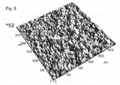
Figure 5 is the Atomic Force Microscopy (AFM) image of the N-type nc-Si:H film inEmbodiment 1 of the present invention. -
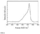
Figure 6 is the Raman line of the I layer nc-Si:H film inEmbodiment 1 of the present invention. -
Figure 7 is the XRD spectral line of the I layer nc-Si:H film inEmbodiment 1 of the present invention. -
Figure 8 is the AFM image of the P-type InxGa1-xN quantum well crystal film inEmbodiment 1 of the present invention. - The embodiments and example of the present invention are described in detail as follows: The crystallization property test of the sample of the present invention is X-ray diffraction analysis during which an instrument of Bruker AXS D8 type is used.
- In the present invention, a RENISHAW in Via Raman Microscope spectrometer is used to test the Raman spectrum of the deposited film, the laser source is a 632.8 nm Ne-He laser, the laser power is 35 mW and the resolution is 2 µm.
- In the present invention, a multifunctional surface analysis system ESCALAB250 produced by the American Thermo VG is used during XPS analysis, and the X-ray source is a target Al Kα (1486.6eV) ray.
- The AFM used in the present invention is
Picoscan 2500 produced by Agilent. The morphology of a film sample is tested and analyzed at normal room temperature. The analyzed area of the film sample is {P1}. - The structure diagram of the solar cell with a stainless steel substrate of an adjustable bandgap quantum well structure of this embodiment is shown in
Figure 1 . The preparation method comprises the steps of: - (1) After ultrasonic cleaning (1a) by ionized water for 5 min, drying up the flexible stainless steel substrate by N2 and putting the substrate into a magnetron sputtering reaction chamber to prepare (1 b) the AlN insulating layer by deposition at a vacuum of 9.0 × 10⁻⁴ Pa; the process parameters are as follows: the reaction source is the gas mixture of Ar and N2, the flow ratio of Ar:N2 is 10:1, the substrate is heated to 100°C, and the deposition time is 30 min. The structure at this time is AlN insulating layer/flexible stainless steel substrate.
- (2) Preparing the Al metal back electrode by magnetron sputtering; the process parameters are as follows: the reaction source is Ar, the flow rate of Ar is 10 sccm, the temperature of the substrate is 50°C, and the deposition time is 3 min. The structure at this time is Al back electrode/AIN insulating layer/flexible stainless steel substrate.
- (3) Preparing one GZO transparent conductive film by the ECR-PEMOCVD system; the process parameters are as follows: Ar carried TMGa, DEZn and O2 are introduced to the reaction chamber, the flow ratio of TMGa:DEZn:O2 is 1:2:80, the microwave power is 650 W, the deposition temperature is 200°C, the deposition pressure is 0.8 Pa, and the deposition time is 10 min. The structure at this time is GZO/Al back electrode/AIN insulating layer/flexible stainless steel substrate.
- (4) Preparing the N-type nc-Si:H film by the ECR-PEMOCVD system and introducing Ar diluted SiH4 and H2 diluted PH3 to the reaction chamber; the process parameters are as follows: the flow rate of Ar diluted SiH4 is 5 sccm, the flow rate of H2 diluted PH3 is 0.5 sccm, the flow rate of H2 is 25 sccm, the microwave power is 650 W, the deposition temperature is 250°C, the deposition pressure is 0.8 Pa, and the deposition time is 30 min. The structure at this time is N-type nc-Si:H/GZO/Al back electrode/AIN insulating layer/flexible stainless steel substrate.
The performance of the P-doped N-type nc-Si:H film is tested and analyzed by an XPS analysis equipment, and the result is shown inFigure 3 . As can be seen fromFigure 3 , the performance of the P-doped N-type nc-Si:H film is good. The structural performance of the P-doped N-type nc-Si:H film is tested and analyzed by a Raman spectrometer, and the result is shown inFigure 4 . As can be seen fromFigure 4 , the structural performance of the P-doped N-type nc-Si:H film is good. The morphology of the P-doped N-type nc-Si:H film is tested and analyzed by an AFM, and the result is shown inFigure 5 . As can be seen fromFigure 5 , the morphology of the P-doped N-type nc-Si:H film is flat, and the distribution of crystal grains is uniform. - (5) Preparing the I layer nc-Si:H intrinsic film by the ECR-PEMOCVD system and introducing Ar diluted SiH4 and H2 to the reaction chamber; the process parameters are as follows: the flow rate of Ar diluted SiH4 is 5 sccm, the flow rate of H2 is 25 sccm, the microwave power is 650 W, the deposition temperature is 250°C, the deposition pressure is 0.8 Pa, and the deposition time is 30 min. The structure at this time is I layer nc-Si:H intrinsic film/N-type nc-Si:H/GZO/Al back electrode/AIN insulating layer/flexible stainless steel substrate.
The structural performance of the non-doped I layer nc-Si:H intrinsic film is tested and analyzed by a Raman spectrometer, and the result is shown inFigure 6 . As can be seen fromFigure 6 , the structural performance of the non-doped I layer nc-Si:H intrinsic film is good. The crystallization property of the non-doped I layer nc-Si:H intrinsic film is tested and analyzed by a XRD spectral line, and the result is shown inFigure 7 . As can be seen fromFigure 7 , the crystallization property of the non-doped I layer nc-Si:H intrinsic film is good. - (6) Preparing the P-type InxGa1-xN adjustable bandgap quantum well crystal film by the ECR-PEMOCVD system and introducing H2 diluted TMGa, TMIn, Mg(C5H5)2 and N2 to the reaction chamber; the process parameters are as follows: the flow ratio of TMGa:TMIn:Mg(C5H5)2 is 8:4:1, the flow rate of N2 is 80 sccm, the microwave power is 650 W, the deposition temperature is 200°C, the deposition pressure is 0.9 Pa, and the deposition time is 40 min. The structure at this time is P-type InxGa1-xN/I layer nc-Si:H intrinsic film/N-type nc-Si:H/GZO/Al back electrode/AIN insulating layer/flexible stainless steel substrate.
The morphology of the Mg-doped P-type InxGa1-xN quantum well crystal film is tested and analyzed by an AFM, and the result is shown inFigure 8 . As can be seen from
Figure 8 , the morphology of the InxGa1-xN quantum well intrinsic crystal film is flat, and the distribution of crystal grains is uniform. - (7) Preparing the other GZO transparent conductive film by the ECR-PEMOCVD system and introducing Ar carried TMGa, DEZn and O2 to the reaction chamber; the process parameters are as follows: the flow ratio of TMGa:DEZn:O2 is 1:2:80, the microwave power is 650 W, the deposition temperature is 200°C, the deposition pressure is 0.8 Pa, and the deposition time is 10 min. The structure at this time is GZO/P-type InxGa1-xN/I layer nc-Si:H intrinsic film/N-type nc-Si:H/GZO/Al back electrode/AIN insulating layer/flexible stainless steel substrate.
- (8) Preparing the Al metal back electrode by magnetron sputtering; the process parameters are as follows: the reaction source is Ar, the flow rate of Ar is 10 sccm, the deposition temperature is 50°C, and the deposition time is 3 min. The structure at this time is Al electrode/GZO/P-type InxGa1-xN/I layer nc-Si:H intrinsic film/N-type nc-Si:H/GZO/Al back electrode/AIN insulating layer/flexible stainless steel substrate.
- The structure diagram of the solar cell with a stainless steel substrate of an adjustable bandgap quantum well structure of this embodiment is shown in
Figure 1 . The preparation method comprises the steps of: - (1) After ultrasonic cleaning (1a) by ionized water for 5 min, drying up the flexible stainless steel substrate by N2 and putting the substrate into a magnetron sputtering reaction chamber to prepare (1 b) the AlN insulating layer by deposition at a vacuum of 9.0 × 10⁻⁴ Pa; the process parameters are as follows: the reaction source is the gas mixture of Ar and N2, the flow ratio of Ar:N2 is 10:1, the substrate is heated to 150°C, and the deposition time is 45 min. The structure at this time is AlN insulating layer/flexible stainless steel substrate.
- (2) Preparing the Al metal back electrode by magnetron sputtering; the process parameters are as follows: the reaction source is Ar, the flow rate of Ar is 12 sccm, the temperature of the substrate is 150°C, and the deposition time is 5 min. The structure at this time is Al back electrode/AIN insulating layer/flexible stainless steel substrate.
- (3) Preparing one GZO transparent conductive film by the ECR-PEMOCVD system; the process parameters are as follows: Ar carried TMGa, DEZn and O2 are introduced to the reaction chamber, the flow ratio of TMGa:DEZn:O2 is 1:2:80, the microwave power is 650 W, the deposition temperature is 250°C, the deposition pressure is 1.0 Pa, and the deposition time is 13 min. The structure at this time is GZO/Al back electrode/AIN insulating layer/flexible stainless steel substrate.
- (4) Preparing the N-type nc-Si:H film by the ECR-PEMOCVD system and introducing Ar diluted SiH4 and H2 diluted PH3 to the reaction chamber; the process parameters are as follows: the flow rate of Ar diluted SiH4 is 6 sccm, the flow rate of H2 diluted PH3 is 3 sccm, the flow rate of H2 is 28 sccm, the microwave power is 650 W, the deposition temperature is 300°C, the deposition pressure is 1.0 Pa, and the deposition time is 40 min. The structure at this time is N-type nc-Si:H/GZO/Al back electrode/AIN insulating layer/flexible stainless steel substrate.
- (5) Preparing the I layer nc-Si:H intrinsic film by the ECR-PEMOCVD system and introducing Ar diluted SiH4 and H2 to the reaction chamber; the process parameters are as follows: the flow rate of Ar diluted SiH4 is 6 sccm, the flow rate of H2 is 26 sccm, the microwave power is 650 W, the deposition temperature is 300°C, the deposition pressure is 1.0 Pa, and the deposition time is 48 min. The structure at this time is I layer nc-Si:H intrinsic film/N-type nc-Si:H/GZO/Al back electrode/AIN insulating layer/flexible stainless steel substrate.
- (6) Preparing the P-type InxGa1-xN adjustable bandgap quantum well crystal film by the ECR-PEMOCVD system and introducing H2 diluted TMGa, TMIn, Mg(C5H5)2 and N2 to the reaction chamber; the process parameters are as follows: the flow ratio of TMGa:TMIn:Mg(C5H5)2 is 8:4:1, the flow rate of N2 is 105 sccm, the microwave power is 650 W, the deposition temperature is 600°C, the deposition pressure is 1.0 Pa, and the deposition time is 50 min. The structure at this time is P-type InxGa1-xN/I layer nc-Si:H intrinsic film/N-type nc-Si:H/GZO/Al back electrode/AIN insulating layer/flexible stainless steel substrate.
- (7) Preparing the other GZO transparent conductive film by the ECR-PEMOCVD system and introducing Ar carried TMGa, DEZn and O2 to the reaction chamber; the process parameters are as follows: the flow ratio of TMGa:DEZn:O2 is 1:2:80, the microwave power is 650 W, the deposition temperature is 400°C, the deposition pressure is 1.0 Pa, and the deposition time is 18 min. The structure at this time is GZO/P-type InxGa1-xN/I layer nc-Si:H intrinsic film/N-type nc-Si:H/GZO/Al back electrode/AIN insulating layer/flexible stainless steel substrate.
- (8) Preparing the Al metal back electrode by magnetron sputtering; the process parameters are as follows: the reaction source is Ar, the flow rate of Ar is 18 sccm, the deposition temperature is 150°C, and the deposition time is 10 min. The structure at this time is Al electrode/GZO/P-type InxGa1-xN/I layer nc-Si:H intrinsic film/N-type nc-Si:H/GZO/Al back electrode/AIN insulating layer/flexible stainless steel substrate.
- The structure diagram of the solar cell with a stainless steel substrate of an adjustable bandgap quantum well structure of this example is shown in
Figure 1 . The preparation method comprises the steps of: - (1) After ultrasonic cleaning (1a) by ionized water for 5 min, drying up the flexible stainless steel substrate by N2 and putting the substrate into a magnetron sputtering reaction chamber to prepare (1 b) the AlN insulating layer by deposition at a vacuum of 9.0 × 10⁻⁴ Pa; the process parameters are as follows: the reaction source is the gas mixture of Ar and N2, the flow ratio of Ar:N2 is 10:1, the substrate is heated to 300°C, and the deposition time is 60 min. The structure at this time is AlN insulating layer/flexible stainless steel substrate.
- (2) Preparing the Al metal back electrode by magnetron sputtering; the process parameters are as follows: the reaction source is Ar, the flow rate of Ar is 20 sccm, the temperature of the substrate is 350°C, and the deposition time is 10 min. The structure at this time is Al back electrode/AIN insulating layer/flexible stainless steel substrate.
- (3) Preparing one GZO transparent conductive film by the ECR-PEMOCVD system; the process parameters are as follows: Ar carried TMGa, DEZn and O2 are introduced to the reaction chamber, the flow ratio of TMGa:DEZn:O2 is 1:2:80, the microwave power is 650 W, the deposition temperature is 400°C, the deposition pressure is 1.2 Pa, and the deposition time is 20 min. The structure at this time is GZO/Al back electrode/AIN insulating layer/flexible stainless steel substrate.
- (4) Preparing the N-type nc-Si:H film by the ECR-PEMOCVD system and introducing Ar diluted SiH4 and H2 diluted PH3 to the reaction chamber; the process parameters are as follows: the flow rate of Ar diluted SiH4 is 8 sccm, the flow rate of H2 diluted PH3 is 5 sccm, the flow rate of H2 is 40 sccm, the microwave power is 650 W, the deposition temperature is 600°C, the deposition pressure is 1.2 Pa, and the deposition time is 80 min. The structure at this time is N-type nc-Si:H/GZO/Al back electrode/AIN insulating layer/flexible stainless steel substrate.
- (5) Preparing the I layer nc-Si:H intrinsic film by the ECR-PEMOCVD system and introducing Ar diluted SiH4 and H2 to the reaction chamber; the process parameters are as follows: the flow rate of Ar diluted SiH4 is 8 sccm, the flow rate of H2 is 40 sccm, the microwave power is 650 W, the deposition temperature is 600°C, the deposition pressure is 1.8 Pa, and the deposition time is 80 min. The structure at this time is I layer nc-Si:H intrinsic film/N-type nc-Si:H/GZO/Al back electrode/AIN insulating layer/flexible stainless steel substrate.
- (6) Preparing the P-type InxGa1-xN adjustable bandgap quantum well crystal film by the ECR-PEMOCVD system and introducing H2 diluted TMGa, TMIn, Mg(C5H5)2 and N2 to the reaction chamber; the process parameters are as follows: the flow ratio of TMGa:TMIn:Mg(C5H5)2 is 8:4:1, the flow rate of N2 is 120 sccm, the microwave power is 650 W, the deposition temperature is 300°C, the deposition pressure is 1.4 Pa, and the deposition time is 60 min. The structure at this time is P-type InxGa1-xN/I layer nc-Si:H intrinsic film/N-type nc-Si:H/GZO/Al back electrode/AIN insulating layer/flexible stainless steel substrate.
- (7) Preparing the other GZO transparent conductive film by the ECR-PEMOCVD system and introducing Ar carried TMGa, DEZn and O2 to the reaction chamber; the process parameters are as follows: the flow ratio of TMGa:DEZn:O2 is 1:2:80, the microwave power is 650 W, the deposition temperature is 300°C, the deposition pressure is 1.2 Pa, and the deposition time is 20 min. The structure at this time is GZO/P-type InxGa1-xN/I layer nc-Si:H intrinsic film/N-type nc-Si:H/GZO/Al back electrode/AlN insulating layer/flexible stainless steel substrate.
- (8) Preparing the Al metal back electrode by magnetron sputtering; the process parameters are as follows: the reaction source is Ar, the flow rate of Ar is 20 sccm, the deposition temperature is 400°C, and the deposition time is 5 min. The structure at this time is Al electrode/GZO/P-type InxGa1-xN/I layer nc-Si:H intrinsic film/N-type nc-Si:H/GZO/Al back electrode/AlN insulating layer/flexible stainless steel substrate.
- The structure diagram of the solar cell with a stainless steel substrate of an adjustable bandgap quantum well structure of this embodiment is shown in
Figure 1 . The preparation method comprises the steps of: - (1) After ultrasonic cleaning (1a) by ionized water for 5 min, drying up the flexible stainless steel substrate by N2 and putting the substrate into a magnetron sputtering reaction chamber to prepare (1 b) the AlN insulating layer by deposition at a vacuum of 9.0 × 10⁻⁴ Pa; the process parameters are as follows: the reaction source is the gas mixture of Ar and N2, the flow ratio of Ar:N2 is 10:1, the substrate is heated to 250°C, and the deposition time is 50 min. The structure at this time is AlN insulating layer/flexible stainless steel substrate.
- (2) Preparing the Al metal back electrode by magnetron sputtering; the process parameters are as follows: the reaction source is Ar, the flow rate of Ar is 18 sccm, the temperature of the substrate is 280°C, and the deposition time is 9 min. The structure at this time is Al back electrode/AIN insulating layer/flexible stainless steel substrate.
- (3) Preparing one GZO transparent conductive film by the ECR-PEMOCVD system; the process parameters are as follows: Ar carried TMGa, DEZn and O2 are introduced to the reaction chamber, the flow ratio of TMGa:DEZn:O2 is 1:2:80, the microwave power is 650 W, the deposition temperature is 380°C, the deposition pressure is 1.1 Pa, and the deposition time is 18 min. The structure at this time is GZO/Al back electrode/AIN insulating layer/flexible stainless steel substrate.
- (4) Preparing the N-type nc-Si:H film by the ECR-PEMOCVD system and introducing Ar diluted SiH4 and H2 diluted PH3 to the reaction chamber; the process parameters are as follows: the flow rate of Ar diluted SiH4 is 7 sccm, the flow rate of H2 diluted PH3 is 4 sccm, the flow rate of H2 is 35 sccm, the microwave power is 650 W, the deposition temperature is 550°C, the deposition pressure is 1.1 Pa, and the deposition time is 70 min. The structure at this time is N-type nc-Si:H/GZO/Al back electrode/AIN insulating layer/flexible stainless steel substrate.
- (5) Preparing the I layer nc-Si:H intrinsic film by the ECR-PEMOCVD system and introducing Ar diluted SiH4 and H2 to the reaction chamber; the process parameters are as follows: the flow rate of Ar diluted SiH4 is 7 sccm, the flow rate of H2 is 36 sccm, the microwave power is 650 W, the deposition temperature is 500°C, the deposition pressure is 1.0 Pa, and the deposition time is 60 min. The structure at this time is I layer nc-Si:H intrinsic film/N-type nc-Si:H/GZO/Al back electrode/AIN insulating layer/flexible stainless steel substrate.
- (6) Preparing the P-type InxGa1-xN adjustable bandgap quantum well crystal film by the ECR-PEMOCVD system and introducing H2 diluted TMGa, TMIn, Mg(C5H5)2 and N2 to the reaction chamber; the process parameters are as follows: the flow ratio of TMGa:TMIn:Mg(C5H5)2 is 8:4:1, the flow rate of N2 is 100 sccm, the microwave power is 650 W, the deposition temperature is 600°C, the deposition pressure is 1.2 Pa, and the deposition time is 50 min. The structure at this time is P-type InxGa1-xN/I layer nc-Si:H intrinsic film/N-type nc-Si:H/GZO/Al back electrode/AIN insulating layer/flexible stainless steel substrate.
- (7) Preparing the other GZO transparent conductive film by the ECR-PEMOCVD system and introducing Ar carried TMGa, DEZn and O2 to the reaction chamber; the process parameters are as follows: the flow ratio of TMGa:DEZn:O2 is 1:2:80, the microwave power is 650 W, the deposition temperature is 300°C, the deposition pressure is 1.1 Pa, and the deposition time is 15 min. The structure at this time is GZO/P-type InxGa1-xN/I layer nc-Si:H intrinsic film/N-type nc-Si:H/GZO/Al back electrode/AlN insulating layer/flexible stainless steel substrate.
- (8) Preparing the Al metal back electrode by magnetron sputtering; the process parameters are as follows: the reaction source is Ar, the flow rate of Ar is 18 sccm, the deposition temperature is 300°C, and the deposition time is 8 min. The structure at this time is Al electrode/GZO/P-type InxGa1-xN/I layer nc-Si:H intrinsic film/N-type nc-Si:H/GZO/Al back electrode/AlN insulating layer/flexible stainless steel substrate.
- The structure diagram of the solar cell with a stainless steel substrate of an adjustable bandgap quantum well structure of this embodiment is shown in
Figure 1 . The preparation method comprises the steps of: - (1) After ultrasonic cleaning (1a) by ionized water for 5 min, drying up the flexible stainless steel substrate by N2 and putting the substrate into a magnetron sputtering reaction chamber to prepare (1b) the AlN insulating layer by deposition at a vacuum of 9.0 × 10⁻⁴ Pa; the process parameters are as follows: the reaction source is the gas mixture of Ar and N2, the flow ratio of Ar:N2 is 10:1, the substrate is heated to 230°C, and the deposition time is 60 min. The structure at this time is AlN insulating layer/flexible stainless steel substrate.
- (2) Preparing the Al metal back electrode by magnetron sputtering; the process parameters are as follows: the reaction source is Ar, the flow rate of Ar is 15 sccm, the temperature of the substrate is 300°C, and the deposition time is 10 min. The structure at this time is Al back electrode/AlN insulating layer/flexible stainless steel substrate.
- (3) Preparing one GZO transparent conductive film by the ECR-PEMOCVD system; the process parameters are as follows: Ar carried TMGa, DEZn and O2 are introduced to the reaction chamber, the flow ratio of TMGa:DEZn:O2 is 1:2:80, the microwave power is 650 W, the deposition temperature is 400°C, the deposition pressure is 1.1 Pa, and the deposition time is 20 min. The structure at this time is GZO/Al back electrode/AIN insulating layer/flexible stainless steel substrate.
- (4) Preparing the N-type nc-Si:H film by the ECR-PEMOCVD system and introducing Ar diluted SiH4 and H2 diluted PH3 to the reaction chamber; the process parameters are as follows: the flow rate of Ar diluted SiH4 is 8 sccm, the flow rate of H2 diluted PH3 is 5 sccm, the flow rate of H2 is 35 sccm, the microwave power is 650 W, the deposition temperature is 500°C, the deposition pressure is 1.1 Pa, and the deposition time is 75 min. The structure at this time is N-type nc-Si:H/GZO/Al back electrode/AIN insulating layer/flexible stainless steel substrate.
- (5) Preparing the I layer nc-Si:H intrinsic film by the ECR-PEMOCVD system and introducing Ar diluted SiH4 and H2 to the reaction chamber; the process parameters are as follows: the flow rate of Ar diluted SiH4 is 7 sccm, the flow rate of H2 is 40 sccm, the microwave power is 650 W, the deposition temperature is 600°C, the deposition pressure is 0.8 Pa, and the deposition time is 70 min. The structure at this time is I layer nc-Si:H intrinsic film/N-type nc-Si:H/GZO/Al back electrode/AIN insulating layer/flexible stainless steel substrate.
- (6) Preparing the P-type InxGa1-xN adjustable bandgap quantum well crystal film by the ECR-PEMOCVD system and introducing H2 diluted TMGa, TMIn, Mg(C5H5)2 and N2 to the reaction chamber; the process parameters are as follows: the flow ratio of TMGa:TMIn:Mg(C5H5)2 is 8:4:1, the flow rate of N2 is 110 sccm, the microwave power is 650 W, the deposition temperature is 600°C, the deposition pressure is 1.2 Pa, and the deposition time is 60 min. The structure at this time is P-type InxGa1-xN/I layer nc-Si:H intrinsic film/N-type nc-Si:H/GZO/Al back electrode/AIN insulating layer/flexible stainless steel substrate.
- (7) Preparing the other GZO transparent conductive film by the ECR-PEMOCVD system and introducing Ar carried TMGa, DEZn and O2 to the reaction chamber; the process parameters are as follows: the flow ratio of TMGa:DEZn:O2 is 1:2:80, the microwave power is 650 W, the deposition temperature is 300°C, the deposition pressure is 1.2 Pa, and the deposition time is 20 min. The structure at this time is GZO/P-type InxGa1-xN/I layer nc-Si:H intrinsic film/N-type nc-Si:H/GZO/Al back electrode/AIN insulating layer/flexible stainless steel substrate.
- (8) Preparing the Al metal back electrode by magnetron sputtering; the process parameters are as follows: the reaction source is Ar, the flow rate of Ar is 20 sccm, the deposition temperature is 300°C, and the deposition time is 8 min. The structure at this time is Al electrode/GZO/P-type InxGa1-xN/I layer nc-Si:H intrinsic film/N-type nc-Si:H/GZO/Al back electrode/AlN insulating layer/flexible stainless steel substrate.
Claims (2)
- A preparation method for the solar cell with a stainless steel substrate of an adjustable bandgap quantum well structure , wherein a stainless steel sheet is used as a flexible substrate, an AlN insulating layer is above the substrate, an Al back electrode is above the AlN insulating layer, a Ga-doped ZnO (GZO) transparent conductive film used as a buffer layer is above the Al back electrode, an N-type hydrogenated nano-crystalline silicon (nc-Si:H) film is above the GZO transparent conductive film, an I layer nc-Si:H intrinsic film is above the N-type nc-Si:H film, a P-type InxGa1-xN film is above the I layer nc-Si:H intrinsic film, another GZO transparent conductive film is above the P-type InxGa1-xN film, and an Al metal electrode is above the GZO transparent conductive film, the specific structure being Al electrode/GZO/P-type InxGa1-xN/I layer nc-Si:H film/N-type nc-Si:H/GZO/Al back electrode/AIN insulating layer/flexible stainless steel substrate, wherein the P-type InxGa1-xN film has an adjustable bandgap width and a quantum well structure, wherein the value of x in the P-type film comprising InxGa1-xN is between 0 and 1, characterized in that it comprises the steps of:(1) After ultrasonic cleaning by ionized water, drying up the flexible stainless steel substrate by N2 and putting the substrate into a magnetron sputtering reaction chamber to prepare the AlN insulating layer by deposition at a vacuum of 9.0 × 10⁻⁴ Pa; the process parameters being as follows: the target material is aluminum, the reaction source is the gas mixture of Ar and N2, the flow ratio of Ar:N2 is 10:1, the substrate is heated to 100 to 300°C, and the deposition time is 30 to 60 min, the structure at this time being AlN insulating layer/flexible stainless steel substrate;(2) Preparing the Al metal back electrode by magnetron sputtering; the process parameters being as follows: the reaction source is Ar, the flow rate of Ar is 10 to 20 sccm, the target material is aluminum, the temperature of the substrate is 50 to 350°C, and the deposition time is 3 to 10 min, the structure at this time being Al back electrode/AIN insulating layer/flexible stainless steel substrate;(3) Preparing one GZO transparent conductive film by an Electron Cyclotron Resonance Plasma Enhanced Chemical Vapor Deposition (ECR-PEMOCVD) system; the process parameters being as follows: Ar carried trimethyl gallium (TMGa), diethyl zinc (DEZn) and O2 are introduced to the reaction chamber, the flow ratio of TMGa:DEZn:O2 is 1:2:80, the microwave power is 650 W, the deposition temperature is 200 to 400°C, the deposition pressure is 0.8 to 1.2 Pa, and the deposition time is 10 to 20 min, the structure at this time being GZO/Al back electrode/AIN insulating layer/flexible stainless steel substrate;(4) Preparing the N-type nc-Si:H film by the ECR-PEMOCVD system and introducing Ar diluted SiH4 and H2 diluted PH3 to the reaction chamber; the process parameters being as follows: the flow rate of Ar diluted SiH4 is 5 to 8 sccm, the flow rate of H2 diluted PH3 is 0.5 to 5 sccm, the flow rate of H2 is 25 to 40 sccm, the microwave power is 650 W, the deposition temperature is 250 to 600°C, the deposition pressure is 0.8 to 1.2 Pa, and the deposition time is 30 to 80 min, the structure at this time being N-type nc-Si:H/GZO/Al back electrode/AIN insulating layer/flexible stainless steel substrate;(5) Preparing the I layer nc-Si:H intrinsic film by the ECR-PEMOCVD system and introducing Ar diluted SiH4 and H2 to the reaction chamber; the process parameters being as follows: the flow rate of Ar diluted SiH4 is 5 to 8 sccm, the flow rate of H2 is 25 to 40 sccm, the microwave power is 650 W, the deposition temperature is 250 to 600°C, the deposition pressure is 0.8 to 1.2 Pa, and the deposition time is 30 to 80 min, the structure at this time being I layer nc-Si:H intrinsic film/N-type nc-Si:H/GZO/Al back electrode/AIN insulating layer/flexible stainless steel substrate.(6) Preparing the P-type InxGa1-xN film by the ECR-PEMOCVD system and introducing H2 diluted trimethyl gallium (TMGa), trimethyl indium (TMIn), ferrocene magnesium (Mg(C5H5)2) and N2 to the reaction chamber; the process parameters being as follows: the flow ratio of TMGa:TMIn:Mg(C5H5)2 is 8:4:1, the flow rate of N2 is 80 to 120 sccm, the microwave power is 650 W, the deposition temperature is 200 to 600°C, the deposition pressure is 0.9 to 1.4 Pa, and the deposition time is 40 to 60 min, the structure at this time being P-type InxGa1-xN/I layer nc-Si:H intrinsic film/N-type nc-Si:H/GZO/Al back electrode/AIN insulating layer/flexible stainless steel substrate;(7) Preparing the other GZO transparent conductive film by the ECR-PEMOCVD system and introducing Ar carried TMGa, DEZn and O2 to the reaction chamber; the process parameters being as follows: the flow ratio of TMGa:DEZn:O2 is 1:2:80, the microwave power is 650 W, the deposition temperature is 200 to 400°C, the deposition pressure is 0.8 to 1.2 Pa, and the deposition time is 10 to 20 min, the structure at this time being GZO/P-type InxGa1-xN/I layer nc-Si:H intrinsic film/N-type nc-Si:H/GZO/Al back electrode/AIN insulating layer/flexible stainless steel substrate;(8) Preparing the Al metal back electrode by magnetron sputtering; the process parameters being as follows: the reaction source is Ar, the flow rate of Ar is 10 to 20 sccm, the target material is aluminum, the deposition temperature is 50 to 400°C, and the deposition time is 3 to 10 min, the structure at this time being Al electrode/GZO/P-type InxGa1-xN/I layer nc-Si:H intrinsic film/N-type nc-Si:H/GZO/Al back electrode/AIN insulating layer/flexible stainless steel substrate.
- The preparation method for the solar cell with a stainless steel substrate of an adjustable bandgap quantum well structure of Claim 1, characterized in that the target material of aluminum used during magnetron sputtering has a purity of 99.99%.
Applications Claiming Priority (1)
| Application Number | Priority Date | Filing Date | Title |
|---|---|---|---|
| CN201310746388.5A CN103746016B (en) | 2013-12-30 | 2013-12-30 | Solar cell and preparation method at the bottom of the stainless steel lining of gap tunable quantum well structure |
Publications (2)
| Publication Number | Publication Date |
|---|---|
| EP2889918A1 EP2889918A1 (en) | 2015-07-01 |
| EP2889918B1 true EP2889918B1 (en) | 2017-08-02 |
Family
ID=50503023
Family Applications (1)
| Application Number | Title | Priority Date | Filing Date |
|---|---|---|---|
| EP14162221.7A Not-in-force EP2889918B1 (en) | 2013-12-30 | 2014-03-28 | Preparation method of solar cell with stainless steel substrate of adjustable bandgap quantum well structure |
Country Status (2)
| Country | Link |
|---|---|
| EP (1) | EP2889918B1 (en) |
| CN (1) | CN103746016B (en) |
Families Citing this family (5)
| Publication number | Priority date | Publication date | Assignee | Title |
|---|---|---|---|---|
| CN105140339B (en) * | 2015-08-05 | 2017-10-13 | 沈阳工程学院 | The flexible substrate film solar cell and preparation method of dlc protective layer structure |
| CN105185861A (en) * | 2015-08-05 | 2015-12-23 | 辽宁恒华航海电力设备工程有限公司 | Glass-structure-based thin-film solar battery and preparation method thereof |
| CN105047740B (en) * | 2015-08-05 | 2017-10-13 | 沈阳工程学院 | A kind of flexible stainless steel structure solar cell of Si bases and preparation method |
| CN106571410A (en) * | 2016-10-17 | 2017-04-19 | 北京四方创能光电科技有限公司 | Full-laser scribing method for flexible stainless steel substrate solar cell module |
| CN112467005A (en) * | 2020-11-18 | 2021-03-09 | 福建中晶科技有限公司 | Preparation method of multi-composite-layer patterned sapphire substrate |
Citations (1)
| Publication number | Priority date | Publication date | Assignee | Title |
|---|---|---|---|---|
| US20120164767A1 (en) * | 2009-08-18 | 2012-06-28 | Commissariat A L'energie Atomique Et Aux Energies Alternatives | Method of manufacturing a light emission device based on light emitting diodes |
Family Cites Families (4)
| Publication number | Priority date | Publication date | Assignee | Title |
|---|---|---|---|---|
| JP2008500723A (en) * | 2004-05-27 | 2008-01-10 | フォブオン・インク | Amorphous silicon vertical color filter |
| US8791359B2 (en) * | 2006-01-28 | 2014-07-29 | Banpil Photonics, Inc. | High efficiency photovoltaic cells |
| US8017415B2 (en) * | 2008-11-05 | 2011-09-13 | Goldeneye, Inc. | Dual sided processing and devices based on freestanding nitride and zinc oxide films |
| CN201754407U (en) * | 2010-04-30 | 2011-03-02 | 华中科技大学 | Silicon-substrate single InGaN (indium gallium nitride) solar battery |
-
2013
- 2013-12-30 CN CN201310746388.5A patent/CN103746016B/en active Active
-
2014
- 2014-03-28 EP EP14162221.7A patent/EP2889918B1/en not_active Not-in-force
Patent Citations (1)
| Publication number | Priority date | Publication date | Assignee | Title |
|---|---|---|---|---|
| US20120164767A1 (en) * | 2009-08-18 | 2012-06-28 | Commissariat A L'energie Atomique Et Aux Energies Alternatives | Method of manufacturing a light emission device based on light emitting diodes |
Non-Patent Citations (1)
| Title |
|---|
| YUN JEONG HWANG ET AL: "Si/InGaN Core/Shell Hierarchical Nanowire Arrays and their Photoelectrochemical Properties", NANO LETTERS, vol. 12, no. 3, 14 March 2012 (2012-03-14), US, pages 1678 - 1682, XP055289737, ISSN: 1530-6984, DOI: 10.1021/nl3001138 * |
Also Published As
| Publication number | Publication date |
|---|---|
| CN103746016B (en) | 2016-03-09 |
| EP2889918A1 (en) | 2015-07-01 |
| CN103746016A (en) | 2014-04-23 |
Similar Documents
| Publication | Publication Date | Title |
|---|---|---|
| Pietruszka et al. | New efficient solar cell structures based on zinc oxide nanorods | |
| Tomakin | Structural and optical properties of ZnO and Al-doped ZnO microrods obtained by spray pyrolysis method using different solvents | |
| CN101627457B (en) | A method and device of diamond like carbon multi-layer doping growth | |
| CN102157577B (en) | Nanometer silicon/monocrystalline silicon heterojunction radial nanowire solar cell and preparation method thereof | |
| EP2889918A1 (en) | Solar cell with stainless steel substrate of adjustable bandgap quantum well structure and preparation method therefor | |
| CN102656707B (en) | Thin-film silicon stacked solar cell and manufacturing method thereof | |
| CN101245447A (en) | Plasma Deposition Method of Nanocrystalline Silicon | |
| EP2889921B1 (en) | Solar cell with flexible substrate of adjustable bandgap quantum well structure and preparation method therefor | |
| CN104362183B (en) | Silicon carbon window layer film with refractive index gradient characteristics and application | |
| Huang et al. | Plasma-produced ZnO nanorod arrays as an antireflective layer in c-Si solar cells | |
| CN101789463A (en) | n-shaped zinc oxide nano rod/p-shaped diamond heterojunction photoelectric device and preparation method | |
| CN1298207A (en) | Semiconductor device and its producing method | |
| Roy et al. | Cross-fertilized biomimetic structures achieved through nanosphere lithography on an ultrathin wafer for flexible black c-Si SHJ solar cells | |
| CN102157617B (en) | Preparation method of silicon-based nano-wire solar cell | |
| Ma et al. | In situ grown size-controlled silicon nanocrystals: A p type nanocrystalline-Si: H/a-SiCx: H superlattice (p-nc-Si: H/a-SiCx: H) approach | |
| Chen et al. | Highly transparent conductive gallium-doped zinc oxide thin films grown by reactive plasma deposition for silicon heterojunction solar cells | |
| Das et al. | Growth mechanism and opto-structural characterization of vertically oriented Si nanowires: implications for heterojunction solar cells | |
| Kunya et al. | Cuprous oxide (Cu2O) based solar cell thickness dependence | |
| CN102983215A (en) | Method for preparing silicon thin-film solar cells with silicon nano-wire structures | |
| Wang et al. | Zinc-tin oxide transparent conductive layers via reactive plasma deposition for silicon heterojunction solar cells | |
| CN106711288B (en) | A kind of preparation method of Nano silicon-crystal thin film solar cell | |
| US20180083161A1 (en) | Direct texture transparent conductive oxide served as electrode or intermediate layer for photovoltaic and display applications | |
| Kuang et al. | Efficient nanorod-based amorphous silicon solar cells with advanced light trapping | |
| Bu et al. | Improved crystalline silicon solar cells by light harvesting zinc oxide nanowire arrays | |
| CN117766640B (en) | Flexible silicon heterojunction solar cell with high photoelectric conversion efficiency and manufacturing method thereof |
Legal Events
| Date | Code | Title | Description |
|---|---|---|---|
| PUAI | Public reference made under article 153(3) epc to a published international application that has entered the european phase |
Free format text: ORIGINAL CODE: 0009012 |
|
| 17P | Request for examination filed |
Effective date: 20140328 |
|
| AK | Designated contracting states |
Kind code of ref document: A1 Designated state(s): AL AT BE BG CH CY CZ DE DK EE ES FI FR GB GR HR HU IE IS IT LI LT LU LV MC MK MT NL NO PL PT RO RS SE SI SK SM TR |
|
| AX | Request for extension of the european patent |
Extension state: BA ME |
|
| R17P | Request for examination filed (corrected) |
Effective date: 20160104 |
|
| RBV | Designated contracting states (corrected) |
Designated state(s): AL AT BE BG CH CY CZ DE DK EE ES FI FR GB GR HR HU IE IS IT LI LT LU LV MC MK MT NL NO PL PT RO RS SE SI SK SM TR |
|
| 17Q | First examination report despatched |
Effective date: 20160726 |
|
| STAA | Information on the status of an ep patent application or granted ep patent |
Free format text: STATUS: EXAMINATION IS IN PROGRESS |
|
| GRAP | Despatch of communication of intention to grant a patent |
Free format text: ORIGINAL CODE: EPIDOSNIGR1 |
|
| STAA | Information on the status of an ep patent application or granted ep patent |
Free format text: STATUS: GRANT OF PATENT IS INTENDED |
|
| INTG | Intention to grant announced |
Effective date: 20170515 |
|
| RIN1 | Information on inventor provided before grant (corrected) |
Inventor name: SONG, SHIWEI Inventor name: LI, YUCAI Inventor name: LIU, BAODAN Inventor name: JU, ZHENHE Inventor name: WANG, JIAN Inventor name: ZHANG, TIEYAN Inventor name: ZHAO, YAN Inventor name: WANG, GANG Inventor name: BIAN, JIMING Inventor name: ZHANG, DONG |
|
| GRAS | Grant fee paid |
Free format text: ORIGINAL CODE: EPIDOSNIGR3 |
|
| GRAA | (expected) grant |
Free format text: ORIGINAL CODE: 0009210 |
|
| STAA | Information on the status of an ep patent application or granted ep patent |
Free format text: STATUS: THE PATENT HAS BEEN GRANTED |
|
| AK | Designated contracting states |
Kind code of ref document: B1 Designated state(s): AL AT BE BG CH CY CZ DE DK EE ES FI FR GB GR HR HU IE IS IT LI LT LU LV MC MK MT NL NO PL PT RO RS SE SI SK SM TR |
|
| REG | Reference to a national code |
Ref country code: CH Ref legal event code: EP Ref country code: AT Ref legal event code: REF Ref document number: 915348 Country of ref document: AT Kind code of ref document: T Effective date: 20170815 |
|
| REG | Reference to a national code |
Ref country code: IE Ref legal event code: FG4D |
|
| REG | Reference to a national code |
Ref country code: DE Ref legal event code: R096 Ref document number: 602014012418 Country of ref document: DE |
|
| REG | Reference to a national code |
Ref country code: NL Ref legal event code: MP Effective date: 20170802 |
|
| REG | Reference to a national code |
Ref country code: AT Ref legal event code: MK05 Ref document number: 915348 Country of ref document: AT Kind code of ref document: T Effective date: 20170802 |
|
| REG | Reference to a national code |
Ref country code: LT Ref legal event code: MG4D |
|
| PG25 | Lapsed in a contracting state [announced via postgrant information from national office to epo] |
Ref country code: LT Free format text: LAPSE BECAUSE OF FAILURE TO SUBMIT A TRANSLATION OF THE DESCRIPTION OR TO PAY THE FEE WITHIN THE PRESCRIBED TIME-LIMIT Effective date: 20170802 Ref country code: HR Free format text: LAPSE BECAUSE OF FAILURE TO SUBMIT A TRANSLATION OF THE DESCRIPTION OR TO PAY THE FEE WITHIN THE PRESCRIBED TIME-LIMIT Effective date: 20170802 Ref country code: FI Free format text: LAPSE BECAUSE OF FAILURE TO SUBMIT A TRANSLATION OF THE DESCRIPTION OR TO PAY THE FEE WITHIN THE PRESCRIBED TIME-LIMIT Effective date: 20170802 Ref country code: AT Free format text: LAPSE BECAUSE OF FAILURE TO SUBMIT A TRANSLATION OF THE DESCRIPTION OR TO PAY THE FEE WITHIN THE PRESCRIBED TIME-LIMIT Effective date: 20170802 Ref country code: SE Free format text: LAPSE BECAUSE OF FAILURE TO SUBMIT A TRANSLATION OF THE DESCRIPTION OR TO PAY THE FEE WITHIN THE PRESCRIBED TIME-LIMIT Effective date: 20170802 Ref country code: NL Free format text: LAPSE BECAUSE OF FAILURE TO SUBMIT A TRANSLATION OF THE DESCRIPTION OR TO PAY THE FEE WITHIN THE PRESCRIBED TIME-LIMIT Effective date: 20170802 Ref country code: NO Free format text: LAPSE BECAUSE OF FAILURE TO SUBMIT A TRANSLATION OF THE DESCRIPTION OR TO PAY THE FEE WITHIN THE PRESCRIBED TIME-LIMIT Effective date: 20171102 |
|
| PG25 | Lapsed in a contracting state [announced via postgrant information from national office to epo] |
Ref country code: IS Free format text: LAPSE BECAUSE OF FAILURE TO SUBMIT A TRANSLATION OF THE DESCRIPTION OR TO PAY THE FEE WITHIN THE PRESCRIBED TIME-LIMIT Effective date: 20171202 Ref country code: GR Free format text: LAPSE BECAUSE OF FAILURE TO SUBMIT A TRANSLATION OF THE DESCRIPTION OR TO PAY THE FEE WITHIN THE PRESCRIBED TIME-LIMIT Effective date: 20171103 Ref country code: RS Free format text: LAPSE BECAUSE OF FAILURE TO SUBMIT A TRANSLATION OF THE DESCRIPTION OR TO PAY THE FEE WITHIN THE PRESCRIBED TIME-LIMIT Effective date: 20170802 Ref country code: LV Free format text: LAPSE BECAUSE OF FAILURE TO SUBMIT A TRANSLATION OF THE DESCRIPTION OR TO PAY THE FEE WITHIN THE PRESCRIBED TIME-LIMIT Effective date: 20170802 Ref country code: ES Free format text: LAPSE BECAUSE OF FAILURE TO SUBMIT A TRANSLATION OF THE DESCRIPTION OR TO PAY THE FEE WITHIN THE PRESCRIBED TIME-LIMIT Effective date: 20170802 Ref country code: BG Free format text: LAPSE BECAUSE OF FAILURE TO SUBMIT A TRANSLATION OF THE DESCRIPTION OR TO PAY THE FEE WITHIN THE PRESCRIBED TIME-LIMIT Effective date: 20171102 Ref country code: PL Free format text: LAPSE BECAUSE OF FAILURE TO SUBMIT A TRANSLATION OF THE DESCRIPTION OR TO PAY THE FEE WITHIN THE PRESCRIBED TIME-LIMIT Effective date: 20170802 |
|
| PG25 | Lapsed in a contracting state [announced via postgrant information from national office to epo] |
Ref country code: DK Free format text: LAPSE BECAUSE OF FAILURE TO SUBMIT A TRANSLATION OF THE DESCRIPTION OR TO PAY THE FEE WITHIN THE PRESCRIBED TIME-LIMIT Effective date: 20170802 Ref country code: RO Free format text: LAPSE BECAUSE OF FAILURE TO SUBMIT A TRANSLATION OF THE DESCRIPTION OR TO PAY THE FEE WITHIN THE PRESCRIBED TIME-LIMIT Effective date: 20170802 Ref country code: CZ Free format text: LAPSE BECAUSE OF FAILURE TO SUBMIT A TRANSLATION OF THE DESCRIPTION OR TO PAY THE FEE WITHIN THE PRESCRIBED TIME-LIMIT Effective date: 20170802 |
|
| REG | Reference to a national code |
Ref country code: DE Ref legal event code: R097 Ref document number: 602014012418 Country of ref document: DE |
|
| PG25 | Lapsed in a contracting state [announced via postgrant information from national office to epo] |
Ref country code: IT Free format text: LAPSE BECAUSE OF FAILURE TO SUBMIT A TRANSLATION OF THE DESCRIPTION OR TO PAY THE FEE WITHIN THE PRESCRIBED TIME-LIMIT Effective date: 20170802 Ref country code: EE Free format text: LAPSE BECAUSE OF FAILURE TO SUBMIT A TRANSLATION OF THE DESCRIPTION OR TO PAY THE FEE WITHIN THE PRESCRIBED TIME-LIMIT Effective date: 20170802 Ref country code: SK Free format text: LAPSE BECAUSE OF FAILURE TO SUBMIT A TRANSLATION OF THE DESCRIPTION OR TO PAY THE FEE WITHIN THE PRESCRIBED TIME-LIMIT Effective date: 20170802 Ref country code: SM Free format text: LAPSE BECAUSE OF FAILURE TO SUBMIT A TRANSLATION OF THE DESCRIPTION OR TO PAY THE FEE WITHIN THE PRESCRIBED TIME-LIMIT Effective date: 20170802 |
|
| PLBE | No opposition filed within time limit |
Free format text: ORIGINAL CODE: 0009261 |
|
| STAA | Information on the status of an ep patent application or granted ep patent |
Free format text: STATUS: NO OPPOSITION FILED WITHIN TIME LIMIT |
|
| 26N | No opposition filed |
Effective date: 20180503 |
|
| PG25 | Lapsed in a contracting state [announced via postgrant information from national office to epo] |
Ref country code: SI Free format text: LAPSE BECAUSE OF FAILURE TO SUBMIT A TRANSLATION OF THE DESCRIPTION OR TO PAY THE FEE WITHIN THE PRESCRIBED TIME-LIMIT Effective date: 20170802 |
|
| REG | Reference to a national code |
Ref country code: CH Ref legal event code: PL |
|
| GBPC | Gb: european patent ceased through non-payment of renewal fee |
Effective date: 20180328 |
|
| PG25 | Lapsed in a contracting state [announced via postgrant information from national office to epo] |
Ref country code: MC Free format text: LAPSE BECAUSE OF FAILURE TO SUBMIT A TRANSLATION OF THE DESCRIPTION OR TO PAY THE FEE WITHIN THE PRESCRIBED TIME-LIMIT Effective date: 20170802 |
|
| REG | Reference to a national code |
Ref country code: BE Ref legal event code: MM Effective date: 20180331 |
|
| REG | Reference to a national code |
Ref country code: IE Ref legal event code: MM4A |
|
| PG25 | Lapsed in a contracting state [announced via postgrant information from national office to epo] |
Ref country code: LU Free format text: LAPSE BECAUSE OF NON-PAYMENT OF DUE FEES Effective date: 20180328 |
|
| PG25 | Lapsed in a contracting state [announced via postgrant information from national office to epo] |
Ref country code: IE Free format text: LAPSE BECAUSE OF NON-PAYMENT OF DUE FEES Effective date: 20180328 |
|
| PG25 | Lapsed in a contracting state [announced via postgrant information from national office to epo] |
Ref country code: CH Free format text: LAPSE BECAUSE OF NON-PAYMENT OF DUE FEES Effective date: 20180331 Ref country code: GB Free format text: LAPSE BECAUSE OF NON-PAYMENT OF DUE FEES Effective date: 20180328 Ref country code: BE Free format text: LAPSE BECAUSE OF NON-PAYMENT OF DUE FEES Effective date: 20180331 Ref country code: LI Free format text: LAPSE BECAUSE OF NON-PAYMENT OF DUE FEES Effective date: 20180331 |
|
| PG25 | Lapsed in a contracting state [announced via postgrant information from national office to epo] |
Ref country code: FR Free format text: LAPSE BECAUSE OF NON-PAYMENT OF DUE FEES Effective date: 20180331 |
|
| PG25 | Lapsed in a contracting state [announced via postgrant information from national office to epo] |
Ref country code: MT Free format text: LAPSE BECAUSE OF NON-PAYMENT OF DUE FEES Effective date: 20180328 |
|
| PG25 | Lapsed in a contracting state [announced via postgrant information from national office to epo] |
Ref country code: TR Free format text: LAPSE BECAUSE OF FAILURE TO SUBMIT A TRANSLATION OF THE DESCRIPTION OR TO PAY THE FEE WITHIN THE PRESCRIBED TIME-LIMIT Effective date: 20170802 |
|
| PG25 | Lapsed in a contracting state [announced via postgrant information from national office to epo] |
Ref country code: PT Free format text: LAPSE BECAUSE OF FAILURE TO SUBMIT A TRANSLATION OF THE DESCRIPTION OR TO PAY THE FEE WITHIN THE PRESCRIBED TIME-LIMIT Effective date: 20170802 |
|
| PG25 | Lapsed in a contracting state [announced via postgrant information from national office to epo] |
Ref country code: HU Free format text: LAPSE BECAUSE OF FAILURE TO SUBMIT A TRANSLATION OF THE DESCRIPTION OR TO PAY THE FEE WITHIN THE PRESCRIBED TIME-LIMIT; INVALID AB INITIO Effective date: 20140328 Ref country code: MK Free format text: LAPSE BECAUSE OF NON-PAYMENT OF DUE FEES Effective date: 20170802 Ref country code: CY Free format text: LAPSE BECAUSE OF FAILURE TO SUBMIT A TRANSLATION OF THE DESCRIPTION OR TO PAY THE FEE WITHIN THE PRESCRIBED TIME-LIMIT Effective date: 20170802 |
|
| PG25 | Lapsed in a contracting state [announced via postgrant information from national office to epo] |
Ref country code: AL Free format text: LAPSE BECAUSE OF FAILURE TO SUBMIT A TRANSLATION OF THE DESCRIPTION OR TO PAY THE FEE WITHIN THE PRESCRIBED TIME-LIMIT Effective date: 20170802 |
|
| PGFP | Annual fee paid to national office [announced via postgrant information from national office to epo] |
Ref country code: DE Payment date: 20230316 Year of fee payment: 10 |
|
| REG | Reference to a national code |
Ref country code: DE Ref legal event code: R119 Ref document number: 602014012418 Country of ref document: DE |
|
| PG25 | Lapsed in a contracting state [announced via postgrant information from national office to epo] |
Ref country code: DE Free format text: LAPSE BECAUSE OF NON-PAYMENT OF DUE FEES Effective date: 20241001 |
|
| PG25 | Lapsed in a contracting state [announced via postgrant information from national office to epo] |
Ref country code: DE Free format text: LAPSE BECAUSE OF NON-PAYMENT OF DUE FEES Effective date: 20241001 |