EP2889897A1 - Semiconductor structure provided with germanium-oxide-containing film on top of germanium layer, and manufacturing method therefor - Google Patents
Semiconductor structure provided with germanium-oxide-containing film on top of germanium layer, and manufacturing method therefor Download PDFInfo
- Publication number
- EP2889897A1 EP2889897A1 EP13830424.1A EP13830424A EP2889897A1 EP 2889897 A1 EP2889897 A1 EP 2889897A1 EP 13830424 A EP13830424 A EP 13830424A EP 2889897 A1 EP2889897 A1 EP 2889897A1
- Authority
- EP
- European Patent Office
- Prior art keywords
- oxide film
- germanium
- film
- germanium layer
- semiconductor structure
- Prior art date
- Legal status (The legal status is an assumption and is not a legal conclusion. Google has not performed a legal analysis and makes no representation as to the accuracy of the status listed.)
- Ceased
Links
Images






Classifications
-
- H—ELECTRICITY
- H10—SEMICONDUCTOR DEVICES; ELECTRIC SOLID-STATE DEVICES NOT OTHERWISE PROVIDED FOR
- H10D—INORGANIC ELECTRIC SEMICONDUCTOR DEVICES
- H10D64/00—Electrodes of devices having potential barriers
- H10D64/01—Manufacture or treatment
- H10D64/013—Manufacture or treatment of electrodes having a conductor capacitively coupled to a semiconductor by an insulator
- H10D64/01356—Manufacture or treatment of electrodes having a conductor capacitively coupled to a semiconductor by an insulator the insulator being formed after the semiconductor body, the semiconductor being a Group IV material and not being silicon, e.g. Ge, SiGe or SiGeC
-
- H—ELECTRICITY
- H10—SEMICONDUCTOR DEVICES; ELECTRIC SOLID-STATE DEVICES NOT OTHERWISE PROVIDED FOR
- H10D—INORGANIC ELECTRIC SEMICONDUCTOR DEVICES
- H10D30/00—Field-effect transistors [FET]
- H10D30/60—Insulated-gate field-effect transistors [IGFET]
-
- H—ELECTRICITY
- H10—SEMICONDUCTOR DEVICES; ELECTRIC SOLID-STATE DEVICES NOT OTHERWISE PROVIDED FOR
- H10D—INORGANIC ELECTRIC SEMICONDUCTOR DEVICES
- H10D64/00—Electrodes of devices having potential barriers
- H10D64/60—Electrodes characterised by their materials
- H10D64/66—Electrodes having a conductor capacitively coupled to a semiconductor by an insulator, e.g. MIS electrodes
- H10D64/68—Electrodes having a conductor capacitively coupled to a semiconductor by an insulator, e.g. MIS electrodes characterised by the insulator, e.g. by the gate insulator
- H10D64/681—Electrodes having a conductor capacitively coupled to a semiconductor by an insulator, e.g. MIS electrodes characterised by the insulator, e.g. by the gate insulator having a compositional variation, e.g. multilayered
- H10D64/685—Electrodes having a conductor capacitively coupled to a semiconductor by an insulator, e.g. MIS electrodes characterised by the insulator, e.g. by the gate insulator having a compositional variation, e.g. multilayered being perpendicular to the channel plane
-
- H—ELECTRICITY
- H10—SEMICONDUCTOR DEVICES; ELECTRIC SOLID-STATE DEVICES NOT OTHERWISE PROVIDED FOR
- H10D—INORGANIC ELECTRIC SEMICONDUCTOR DEVICES
- H10D64/00—Electrodes of devices having potential barriers
- H10D64/60—Electrodes characterised by their materials
- H10D64/66—Electrodes having a conductor capacitively coupled to a semiconductor by an insulator, e.g. MIS electrodes
- H10D64/68—Electrodes having a conductor capacitively coupled to a semiconductor by an insulator, e.g. MIS electrodes characterised by the insulator, e.g. by the gate insulator
- H10D64/691—Electrodes having a conductor capacitively coupled to a semiconductor by an insulator, e.g. MIS electrodes characterised by the insulator, e.g. by the gate insulator comprising metallic compounds, e.g. metal oxides or metal silicates
-
- H—ELECTRICITY
- H10—SEMICONDUCTOR DEVICES; ELECTRIC SOLID-STATE DEVICES NOT OTHERWISE PROVIDED FOR
- H10P—GENERIC PROCESSES OR APPARATUS FOR THE MANUFACTURE OR TREATMENT OF DEVICES COVERED BY CLASS H10
- H10P14/00—Formation of materials, e.g. in the shape of layers or pillars
- H10P14/60—Formation of materials, e.g. in the shape of layers or pillars of insulating materials
- H10P14/63—Formation of materials, e.g. in the shape of layers or pillars of insulating materials characterised by the formation processes
- H10P14/6302—Non-deposition formation processes
- H10P14/6304—Formation by oxidation, e.g. oxidation of the substrate
- H10P14/6306—Formation by oxidation, e.g. oxidation of the substrate of the semiconductor materials
- H10P14/6308—Formation by oxidation, e.g. oxidation of the substrate of the semiconductor materials of Group IV semiconductors
-
- H—ELECTRICITY
- H10—SEMICONDUCTOR DEVICES; ELECTRIC SOLID-STATE DEVICES NOT OTHERWISE PROVIDED FOR
- H10P—GENERIC PROCESSES OR APPARATUS FOR THE MANUFACTURE OR TREATMENT OF DEVICES COVERED BY CLASS H10
- H10P14/00—Formation of materials, e.g. in the shape of layers or pillars
- H10P14/60—Formation of materials, e.g. in the shape of layers or pillars of insulating materials
- H10P14/63—Formation of materials, e.g. in the shape of layers or pillars of insulating materials characterised by the formation processes
- H10P14/6302—Non-deposition formation processes
- H10P14/6322—Formation by thermal treatments
-
- H—ELECTRICITY
- H10—SEMICONDUCTOR DEVICES; ELECTRIC SOLID-STATE DEVICES NOT OTHERWISE PROVIDED FOR
- H10P—GENERIC PROCESSES OR APPARATUS FOR THE MANUFACTURE OR TREATMENT OF DEVICES COVERED BY CLASS H10
- H10P14/00—Formation of materials, e.g. in the shape of layers or pillars
- H10P14/60—Formation of materials, e.g. in the shape of layers or pillars of insulating materials
- H10P14/66—Formation of materials, e.g. in the shape of layers or pillars of insulating materials characterised by the type of materials
- H10P14/662—Laminate layers, e.g. stacks of alternating high-k metal oxides
-
- H—ELECTRICITY
- H10—SEMICONDUCTOR DEVICES; ELECTRIC SOLID-STATE DEVICES NOT OTHERWISE PROVIDED FOR
- H10P—GENERIC PROCESSES OR APPARATUS FOR THE MANUFACTURE OR TREATMENT OF DEVICES COVERED BY CLASS H10
- H10P14/00—Formation of materials, e.g. in the shape of layers or pillars
- H10P14/60—Formation of materials, e.g. in the shape of layers or pillars of insulating materials
- H10P14/68—Organic materials, e.g. photoresists
-
- H—ELECTRICITY
- H10—SEMICONDUCTOR DEVICES; ELECTRIC SOLID-STATE DEVICES NOT OTHERWISE PROVIDED FOR
- H10P—GENERIC PROCESSES OR APPARATUS FOR THE MANUFACTURE OR TREATMENT OF DEVICES COVERED BY CLASS H10
- H10P14/00—Formation of materials, e.g. in the shape of layers or pillars
- H10P14/60—Formation of materials, e.g. in the shape of layers or pillars of insulating materials
- H10P14/69—Inorganic materials
- H10P14/692—Inorganic materials composed of oxides, glassy oxides or oxide-based glasses
- H10P14/6938—Inorganic materials composed of oxides, glassy oxides or oxide-based glasses the material containing at least one metal element, e.g. metal oxides, metal oxynitrides or metal oxycarbides
- H10P14/6939—Inorganic materials composed of oxides, glassy oxides or oxide-based glasses the material containing at least one metal element, e.g. metal oxides, metal oxynitrides or metal oxycarbides characterised by the metal
-
- H—ELECTRICITY
- H10—SEMICONDUCTOR DEVICES; ELECTRIC SOLID-STATE DEVICES NOT OTHERWISE PROVIDED FOR
- H10D—INORGANIC ELECTRIC SEMICONDUCTOR DEVICES
- H10D62/00—Semiconductor bodies, or regions thereof, of devices having potential barriers
- H10D62/80—Semiconductor bodies, or regions thereof, of devices having potential barriers characterised by the materials
- H10D62/83—Semiconductor bodies, or regions thereof, of devices having potential barriers characterised by the materials being Group IV materials, e.g. B-doped Si or undoped Ge
Definitions
- the present invention relates to a semiconductor structure having a film including germanium oxide on a germanium layer and a fabricating method of the semiconductor structure.
- Germanium (Ge) is a semiconductor that has better electronic property than silicon (Si).
- germanium oxide for example, GeO 2
- MOSFET Metal Oxide Semiconductor Field Effect Transistor
- Non-patent documents 1 and 2 disclose that an interface condition between a germanium substrate and a germanium oxide film is improved when high pressure oxygen gas is used during forming the germanium oxide film on the germanium substrate.
- Non-Patent Documents 1 and 2 an interface condition between a germanium substrate and a germanium oxide film is preferable. However, a forming rate of the germanium oxide film is large. It is therefore difficult to form a thin germanium oxide film.
- An object of the present invention is to make an interface condition between a germanium layer and a film including germanium oxide preferable and form a film including thin germanium oxide.
- the present invention is a semiconductor structure characterized by including: a germanium layer; and an insulating film that has a film that includes a germanium oxide and is formed on the germanium layer and a high dielectric oxide film that is formed on the film including the germanium oxide and has a dielectric constant higher than that of a silicon oxide, wherein: an EOT of the insulating film is 2 nm or less; and on a presumption that an Au acting as a metal film is formed on the insulating film, a leak current density is 10 -5 X EOT + 4 A/cm 2 or less in a case where a voltage of the metal film with respect to the germanium layer is applied from a flat band voltage to an accumulation region side by 1 V. According to the present invention, it is possible to make an interface condition between a germanium layer and a film including germanium oxide preferable and form a film including thin germanium oxide.
- the high dielectric oxide film may include at least one of a hafnium oxide film, a zirconium oxide film, an aluminum oxide film, an yttrium oxide film, a scandium oxide film and an oxide film of a rare earth element.
- a capacitance value between the germanium layer and the metal film at a frequency of 50 kHz or more may decrease evenly or may be constant when the voltage of the metal film with respect to the germanium layer changes from the flat band voltage to an inversion region.
- the above-mentioned structure may include a gate electrode on the high dielectric oxide film.
- log 10 ⁇ eff (cm 2 /V ⁇ s) may be more than-0.59 X log 10 N s + 10.19 when N s is 5 X 10 12 cm -2 or more in a case where the germanium layer is a p-type, a face current density in the germanium layer is N s (cm -2 ) and an electron mobility of the germanium layer is ⁇ eff (cm 2 /V ⁇ s).
- the present invention is a semiconductor structure characterized by including: a germanium layer; and a germanium oxide film that is formed on the germanium layer, has a density of 3.6 g/cm 3 or more and has an EOT of 2 nm or less. According to the present invention, it is possible to make an interface condition between a germanium layer and a film including germanium oxide preferable and form a film including thin germanium oxide.
- a capacitance value between the germanium layer and the metal film at a frequency of 50 kHz or more may decrease evenly or may be constant when a voltage of the metal film with respect to the germanium layer changes from a flat band voltage to an inversion region.
- the above-mentioned structure may include a gate electrode on the germanium oxide film.
- the present invention is a fabricating method of a semiconductor structure characterized by including: a process of forming a high dielectric oxide film on a germanium layer, a dielectric constant of the high dielectric oxide film being larger than that of a silicon oxide; and a process of forming a film including a germanium oxide between the germanium layer and the high dielectric oxide film by oxidizing the germanium layer through the high dielectric oxide film in an oxygen atmosphere under a condition that a partial pressure of the oxygen at a room temperature is more than 1 atmosphere and a temperature of the germanium layer is less than 550 degrees C.
- the condition may be that the partial pressure of the oxygen at the room temperature is more than 10 atmospheres and the temperature of the germanium layer is 520 degrees C or less.
- the high dielectric oxide film may include at least one of a hafnium oxide film, a zirconium oxide film, an aluminum oxide film, an yttrium oxide film, a scandium oxide film and an oxide film of a rare earth element.
- the above-mentioned method may include a process of forming a gate electrode on the high dielectric oxide film.
- the above-mentioned method may include a process of forming a gate electrode on the high dielectric oxide film, wherein: the condition may be that the partial pressure of the oxygen at the room temperature is more than 10 atmospheres and the temperature of the germanium layer is 520 degrees C or less, and the high dielectric oxide film may be an yttrium oxide.
- the present invention is a fabricating method of a semiconductor structure characterized by including a process of forming a germanium oxide film on the germanium layer by oxidizing an upper face of the germanium layer in an oxygen atmosphere under a condition that a partial pressure of the oxygen at a room temperature is more than 1 atmosphere and a temperature of the germanium layer is less than 550 degrees C. According to the present invention, it is possible to make an interface condition between a germanium layer and a film including germanium oxide preferable and form a film including thin germanium oxide.
- the condition may be that the partial pressure of the oxygen at the room temperature is more than 10 atmospheres and the temperature of the germanium layer is 520 degrees C or less.
- the above-mentioned method may include a process of forming a gate electrode on the germanium oxide film.
- FIG. 1A to FIG. 1C illustrate cross sectional views for describing a fabricating method of a semiconductor structure.
- a germanium substrate 10 is prepared.
- the germanium substrate 10 is a p-type in which a main face is a (100) face, a dopant is gallium (Ga), and a dopant concentration is approximately 7 X 10 16 cm -3 .
- the germanium substrate 10 is subjected to a thermal oxidation in oxygen atmosphere, and thereby a germanium oxide film 12 is formed.
- FIG. 1A a germanium substrate 10 is prepared.
- the germanium substrate 10 is a p-type in which a main face is a (100) face, a dopant is gallium (Ga), and a dopant concentration is approximately 7 X 10 16 cm -3 .
- the germanium substrate 10 is subjected to a thermal oxidation in oxygen atmosphere, and thereby a germanium oxide film 12 is formed.
- FIG. 1A a germanium substrate 10
- an aluminum (Al) film acting as a metal film 16 is formed on a back face of the germanium substrate 10.
- a gold (Au) film acting as a metal film 14 is formed on a front face of the germanium oxide film 12. It is possible to correct a voltage applied to the metal film 14 in a case where a metal other than Au is used as the metal film 14 to a voltage in a case where a work function of the metal film 14 is used and Au is used as the metal film 14.
- FIG. 1B a temperature of the germanium substrate 10 (a substrate temperature) and a pressure of oxygen gas (oxygen pressure) are changed, and the germanium oxide film 12 was formed.
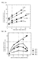
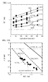
- FIG. 2A illustrates a film thickness of a germanium oxide film with respect to a thermal process time (oxidation time).
- FIG. 2B illustrates a film thickness of a germanium oxide film with respect to an oxygen pressure.
- the substrate temperature is 500 degrees C.
- the oxidation time is 30 minutes.
- Dots of FIG. 2A and FIG. 2B indicate measurement points. And a straight line indicates an approximate line of the measurement points.
- the oxygen pressure is a pressure in a room temperature (approximately 25 degrees C).
- the film thickness of the germanium oxide film 12 increases as the oxidation time passes.
- An inclination of FIG. 2A corresponds to an oxidation rate. This is because oxygen diffuses in the germanium oxide film 12, and the oxygen oxidizes the upper face of the germanium substrate 10.
- the oxidation rate gets higher under a condition that the oxygen pressure is 1 atmosphere than a condition that the oxygen pressure is 0.1 atmospheres. When the oxygen pressure is higher than 1 atmosphere, the oxidation rate gets smaller as the oxygen pressure gets higher.
- the film thickness of the germanium oxide film 12 increases as the oxygen pressure gets higher. This corresponds to the fact that the oxidation rate increases as the oxygen pressure gets higher.
- the film thickness of the germanium oxide film 12 decreases as the oxygen pressure gets higher.
- the oxidation rate is supposed to increase as the oxygen pressure gets higher.
- the above-mentioned interpretation cannot explain the phenomenon that the oxidation rate decreases as the oxygen pressure gets higher.
- an etching rate of the germanium oxide film 12 was measured.
- Samples of FIG. 1B were fabricated. The fabrication conditions are as follows. Oxygen pressure: 70 atmospheres, and substrate temperature: 500 degrees C Oxygen pressure: 70 atmospheres, and substrate temperature: 550 degrees C Oxygen pressure: 1 atmosphere, and substrate temperature: 500 degrees C
- the samples were immersed in mixed liquid of ethyl alcohol (C 2 H 5 OH) and water (H 2 O) with a ratio of 100:5, and the etching rate of the film thickness of the germanium oxide was measured.
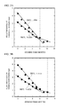
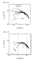
- FIG. 3A and FIG. 3B illustrate the film thickness of the germanium oxide with respect to the etching rate. Dots indicate measurement points.
- Absolute values of the inclinations of FIG. 3A and FIG. 3B correspond to the etching rate.
- the etching rate is approximately 0.56 nm/minute.
- the etching rate is approximately 0.37 nm/minute until five minutes of the etching time. After the five minutes, the etching rate is approximately 0.19 nm/minute.
- the etching rate is approximately 0.62 nm/minute.
- FIG. 4A and FIG. 4B illustrate signal intensity of the samples in which the oxygen pressures are 1 atmosphere and 70 atmospheres with respect to bonding energy.
- the bonding energy of Ge3d was measured.
- peaks of approximately 30 eV correspond to the bonding energy between Ge and Ge.
- Peaks of approximately 33.5 eV correspond to the bonding of Ge and O.
- fabricated samples were samples in which the substrate temperature was 500 degrees C, the film thickness was 5 nm and the oxygen pressure was changed and samples in which the substrate temperature was 550 degrees, the film thickness was 10 nm and the oxygen pressure was changed.
- the density of the germanium oxide film 12 of the fabricated samples was measured with use of a GIXR (Grazing Incidence X-ray Reflectivity) method.
- FIG. 5 illustrates the density of the germanium oxide film with respect to the oxygen pressure. Dots indicate measurement points. Straight lines connect the measurement points. Bars of an upper side and a down side indicate a measurement error. As illustrated in FIG.
- the oxidation rate of the germanium oxide film 12 is small under the condition that the substrate temperature is 520 degrees C or less and the oxygen pressure is 1 atmosphere or more in FIG. 2B because the density of the germanium oxide film 12 is large. It is thought that this is because the germanium oxide film 12 having large density is dense, and thereby the diffusion rate of the oxygen in the germanium oxide film 12 is small.
- FIG. 6 illustrates a leak current with respect to an EOT.
- the measurement temperature is a room temperature.
- the EOT indicates an EOT of the germanium oxide film.
- the EOT can be converted from the saturated capacitance value of the C-V characteristic.
- the leak current density J is a leak current density between the metal film 16 and the metal film 14 in case where the voltage of the metal film 14 with respect to the metal film 16 is -1 V from the flat band voltage. Dots indicate measurement points. Straight lines indicate approximate lines. A dotted line indicates the leak current density with respect to the EOT of the silicon oxide film formed on the silicon substrate.
- the oxidation rate of the samples in which the oxygen pressure is 1 atmosphere and the substrate temperature is 500 degrees C is large. It is therefore difficult to form the germanium oxide film 12 of which EOT is 2.8 nm or less.
- the leak current of an identical EOT is larger than that of the silicon oxide film.
- the oxidation rate of the samples in which the oxygen pressure is 70 atmospheres and the substrate temperature is 550 degrees C is large. It is therefore not possible to form the germanium oxide film 12 of which EOT is 2.2 nm or less.
- the leak current of an identical EOT is smaller than that of the silicon oxide film. However, when the EOT gets smaller, the leak current gets larger.
- the oxidation rate of the samples in which the oxygen pressure is 70 atmospheres and the substrate temperature is 500 degrees C is small. It is therefore possible to form the germanium oxide film 12 of which EOT is approximately 1.2 nm. And, the leak current density J can be 10 -2 A/cm 2 . This value is smaller than a silicon oxide film having the same EOT by approximately 3 digits.
- FIG. 7 illustrates a capacitance value C with respect to the voltage V.
- the measurement temperature is a room temperature.
- the frequency at which the C-V characteristic was measured is 1 kHz to 1 MHz.
- a hysteresis is hardly observed from the region in which the voltage V is minus (accumulation region) to the flat band voltage in which the capacitance value C is reduced.
- the frequency dependence is hardly observed. This indicates that there are extremely few defects in the germanium oxide film 12 and the interface state density on the valence band side of germanium between the germanium substrate 10 and the germanium oxide film 12 is extremely small.
- the capacitance when the voltage is increased to the plus region (inversion region) from the flat band voltage, the capacitance hardly changes with respect to the voltage V and there is no frequency dependence in a region of which frequency is high (1MHz, 100kHz, 50kHz). That is, when the voltage changes from the flat band voltage to the inversion region, the capacitance value between the germanium substrate 10 and the metal film 14 at the frequency of 50 kHz or more decreases evenly or is constant. For example, when the germanium oxide film 12 is formed at 1 atmosphere, the capacitance value at the frequency of 50 kHz or more increases from the flat band voltage to the inversion region as well as the case of the capacitance value at the frequency of 10 kHz or less of FIG. 7 . From the result, it is understood that the interface state density on the conduction band of the germanium at the interface between the germanium substrate 10 and the germanium oxide film 12 is small and the interface condition is preferable, when the germanium oxide film 12 is formed at a high pressure.
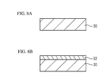
- FIG. 8A and FIG. 8B illustrate cross sectional views for describing a fabricating method of a semiconductor structure in accordance with a first embodiment.
- a germanium layer 30 is prepared.
- the germanium layer 30 may be a single crystal germanium substrate or a germanium film formed on a substrate (for example, a silicon substrate).
- the germanium layer 30 may be a highly-pure germanium or may include an impurity.
- the germanium layer 30 may be an n-type or a p-type germanium.
- the germanium layer 30 may include some amounts of silicon that achieves the effect of the above-mentioned experiments.
- a composition ratio of the silicon may be 10 atomic % or less of the whole.
- a main face of the germanium layer 30 may be a (111) face or the like and may be another crystal face such as a (110) face or a (100) face.
- a germanium oxide film 32 is formed on the germanium layer 30.
- the germanium oxide film 32 may be GeO 2 having a stoichiometric composition ratio or having non-stoichiometric composition ratio.
- the oxygen pressure is higher than 1 atmosphere in FIG. 2B , the forming rate of the germanium oxide film 32 can be smaller than that of the case of the 1 atmosphere.
- the germanium oxide film 12 is formed with such oxidation temperature and such oxygen pressure, it is possible to reduce the EOT and make the interface condition preferable.
- the germanium oxide film 32 oxidizes the upper face of the germanium layer 30 in oxygen atmosphere under a condition that the oxygen partial pressure at a room temperature is larger than 1 atmosphere and the temperature of the germanium layer 30 is less than 550 degrees C as illustrated in FIG. 2B .
- the oxygen partial pressure at a room temperature is larger than 1 atmosphere and the temperature of the germanium layer 30 is less than 550 degrees C as illustrated in FIG. 2B .
- FIG. 6 it is possible to reduce the oxidation rate and form the germanium oxide film 32 having a small EOT with high controllability.
- FIG. 7 it is possible to make the interface condition between the germanium layer 30 and the germanium oxide film 32 preferable. In the experiments, 100% oxygen gas was used.
- mixed gas of oxygen gas and inert gas for example, nitrogen gas, eighteenth group element gas such as helium, neon, argon, krypton, xenon or radon, or mixed gas of these
- the oxygen partial pressure is 10 atmosphere or more. It is more preferable that the oxygen partial pressure is 30 atmospheres or more. It is preferable that the temperature is 520 degrees C or less. It is more preferable that the temperature is 500 degrees C or less. It is preferable that the oxidation temperature is 450 degrees C or more in order to make the interface between the germanium layer 30 and the germanium oxide film 32 preferable. It is more preferable that the oxidation temperature is 470 degrees C or more.
- the germanium oxide film 32 formed in this manner can have the density of 3.6 g/cm 3 or more as illustrated in FIG. 5 and can have the EOT of 2 nm or less as illustrated in FIG. 6 . It is preferable that the density is 3.65 g/cm 3 or more. It is more preferable that the density is 3.7 g/cm 3 or more. It is much more preferable that the density is 3.8 g/cm 3 or more. It is preferable that the EOT is 1.5 nm or less. It is more preferable that the EOT is 1.2 nm or less. It is much more preferable that the EOT is 1.0 nm or less.
- FIG. 9A to FIG. 9D illustrate cross sectional views for describing a fabricating method of a semiconductor structure in accordance with a second embodiment.
- the germanium layer 30 is prepared as well as the first embodiment.
- a high dielectric oxide film 34 is formed on the germanium layer 30.
- the high dielectric oxide film 34 is a film having a dielectric constant higher than that of silicon oxide and is a film including at least one of a hafnium oxide film, a zirconium oxide film, an aluminum oxide film and an oxide film of a rare-earth element (for example, an yttrium oxide film or a scandium oxide film).
- the high dielectric oxide film 34 may be one of the above-mentioned films or a film in which a plurality of above-mentioned films are laminated.
- the rare-earth element is scandium (Sc), yttrium (Y), lanthanum (La), cerium (Ce), praseodymium (Pr), neodymium (Nd), promethium (Pm), samarium (Sm), europium (Eu), gadolinium (Gd), terbium (Tb), dysprosium (Dy), holmium (Ho), erbium (Er), thulium (Tm), ytterbium (Yb), or lutetium (Lu).
- the high dielectric oxide film 34 may have a stoichiometric composition ratio or non-stoichiometric composition ratio.
- the high dielectric oxide film 34 is formed by a sputtering method or the like.
- the high dielectric oxide film 34 is subjected to a thermal process in high pressure oxygen atmosphere. Oxygen diffuses in the high dielectric oxide film 34 and oxidizes an upper face of the germanium layer 30. Thus, the germanium oxide film 32 is formed between the germanium layer 30 and the high dielectric oxide film 34. The germanium oxide film 32 and the high dielectric oxide film 34 form an insulating film 33.
- the germanium oxide film 32 may be GeO 2 having a stoichiometric composition ratio or having non-stoichiometric composition ratio. Atomic elements of the high dielectric oxide film 34 may diffuse in the germanium oxide film 32.
- the germanium oxide film 32 may be a mixed film of germanium oxide and metal oxide (oxide of a metal included in the high dielectric oxide film 34). In this manner, the germanium oxide film 32 may be a film including at least germanium oxide.
- the germanium oxide film 32 oxidizes the upper face of the germanium layer 30 in oxygen atmosphere under a condition that the oxygen partial pressure at a room temperature is more than 1 atmosphere and the oxidation temperature of the germanium layer 30 is less than 550 degrees C as well as the first embodiment. It is preferable that the oxygen partial pressure is 10 atmospheres or more. It is more preferable that the oxygen partial pressure is 30 atmospheres or more. It is preferable that the temperature is 520 degrees C or less. It is more preferable that the temperature is 500 degrees C or less. It is preferable that the oxidation temperature is 450 degrees C or more. It is more preferable that the oxidation temperature is 470 degrees C or more.
- the high dielectric oxide film 34 has a high dielectric constant. It is therefore possible to reduce the EOT of the high dielectric oxide film 34. However, an interface state is formed at an interface between the germanium layer 30 and the high dielectric oxide film 34, and the interface condition is not preferable. And so, as illustrated in FIG. 9C , the upper face of the germanium layer 30 is oxidized through the high dielectric oxide film 34. Thus, the germanium oxide film 32 is formed. Oxygen diffuses in the high dielectric oxide film 34 more easily than the germanium oxide film 32. Therefore, it is possible to form the germanium oxide film 32 with the same condition as the first embodiment. Thus, it is possible to reduce the film thickness of the germanium oxide film 32 and make the interface condition between the germanium layer 30 and the insulating film 33 preferable, as well as the first embodiment.
- the p-type germanium substrate was used as the germanium layer 30
- the yttrium oxide film was used as the high dielectric oxide film 34
- a semiconductor structure was fabricated.
- a metal film 36 (a gold film) was formed on the high dielectric oxide film 34.
- the film thickness of the high dielectric oxide film 34 is 1.5 nm.
- a forming condition of the germanium oxide film 32 is that the oxygen pressure is 70 atmospheres, the substrate temperature is 500 degrees C and the oxidation time is one minute.
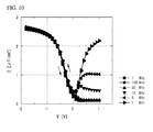
- FIG. 10 illustrates the capacitance C with respect to the voltage V.
- the measurement temperature is a room temperature.
- the frequency for measuring the C-V characteristic is 1 kHz to 1 MHz.
- the hysteresis is hardly observed in a region where the voltage V increases and the capacitance C decreases (a region where an inversion layer is formed from the flat band).
- the capacitance value hardly changes with respect to the voltage V and there is no frequency dependence in the region having high frequencies (1 MHz, 100 kHz and 50 kHz).
- the capacitance value between the germanium substrate 10 and the metal film 14 at a frequency of 50 kHz or more decreases evenly or is constant.
- the interface condition is preferable.
- FIG. 11A illustrates the CET with respect to the oxidation time. Dots are measurement points. Straight lines indicate lines connecting the dots.
- FIG. 11A when the oxygen pressure is enlarged and the substrate temperature is reduced as well as FIG. 2A , the dependence of the CET with respect to the oxidation time is reduced and the control of the CET gets easier. For example, it is possible to reduce the dependence of the CET with respect to the oxidation time under a condition that the substrate temperature is 530 degrees C or less and the oxygen pressure is 10 atmospheres or less.
- FIG. 11B illustrates the leak current density J with respect to the EOT.
- dots indicate the results of the second embodiment.
- Broken lines indicate the results with respect to zirconium oxide (ZrO 2 ) on germanium (Ge), aluminum oxide (Al 2 O 3 ) on germanium oxide (GeO 2 ), lanthanum aluminum oxide (LaAlO 3 ) on strontium germanium (SrGe x ) and silicon oxide (SiO 2 ) on silicon (Si) using a gate electrode of poly-crystal silicon (Poly Si).
- the leak current is smaller than that of the silicon oxide film.
- the leak current is smaller than other embodiments.
- Even if the EOT is 1nm, the leak current density J can be approximately 1 X 10 -3 A/cm 2 .
- the leak current density of the second embodiment is 10 -5 X EOT + 2 A/cm 2 .
- a p-type germanium substrate was used as the germanium layer 30, an yttrium oxide film was used as the high dielectric oxide film 34, and a semiconductor structure was fabricated.
- the film thickness of the high dielectric oxide film 34 is 1.5 nm.
- the forming condition of the germanium oxide film 32 is that the oxygen pressure is 70 atmospheres and the substrate temperature is 500 degrees C. Samples having various EOTs were fabricated by changing the oxidation time. As comparative examples, samples that did not have the high dielectric oxide film 34 and had a germanium oxide film of which EOT was 10 nm were fabricated on the p-type germanium substrate.
- FIG. 12A illustrates an interface state density Dit with respect to the EOT.
- FIG. 12B illustrates the interface state density Dit with respect to the energy.
- the EOT and the interface state density were measured from the impedance measurements at 200K and 100K with use of a conductance method.
- dots indicate an interface state density at -0.2 eV from the mid gap (a center energy of an energy band).
- a solid line indicates an approximate line.
- the interface state density is 2 X 10 11 eV -1 cm -2 or less.
- circle dots indicate the second embodiment in which the EOT is 1 nm.
- the EOT of the insulating film 33 can be 2 nm or less. And, on a presumption that a metal film is formed on the insulating film 33, a leak current density can be 10 -5 X EOT + 4 A/cm 2 or less in a case where the voltage V of the metal film 36 with respect to the germanium layer 30 is -1 V from the flat band voltage. It is preferable that the EOT is 1.5 nm or less. It is more preferable that the EOT is 1.2 nm or less. It is much more preferable that the EOT is 1.0 nm or less. It is preferable that the leak current density is 10 -5 X EOT + 3 A/cm 2 or less.
- leak current density is 1 X 10 -2 A/cm 2 or less. It is much more preferable that the leak current density is 1 X 10 -3 A/cm 2 or less and 1 X 10 -4 A/cm 2 or less.
- the leak current is very large in a case where the EOT is 2 nm or less. In this case, when the EOT is 2 nm or less, it is not possible to reduce the leak current less than the silicon oxide on the silicon substrate having the poly-crystal silicon acting as the gate electrode.
- the leak current density in a case where the voltage of the metal film with respect to the germanium layer was -1 V from the flat band voltage was used for the comparison.
- the leak current density in a case where the voltage of the metal film with respect to the germanium layer is 1V from the flat band voltage is used for the comparison. That is, the leak current density for the comparison is the voltage in a case where the voltage of the metal film with respect to the germanium layer is applied to the accumulation region side from the flat band voltage by 1 V.
- FIG. 13A illustrates a cross sectional view of a transistor having the semiconductor structure of the first embodiment.
- FIG. 13B illustrates a cross sectional view having the semiconductor structure of the second embodiment.
- a gate electrode 38 is formed on the germanium oxide film 32 above the germanium layer 30.
- a source or drain region 40 is formed in the germanium layers 30 on the both sides of the gate electrode 38.
- the germanium layer 30 is a p-type.
- the source or drain region 40 is an n-type.
- the germanium layer 30 may be an n-type and the source or drain region 40 may be a p-type.
- the high dielectric oxide film 34 is formed between the germanium oxide film 32 and the gate electrode 38.
- Other structures are the same as FIG. 13A . Therefore, an explanation of the structures is omitted.
- the germanium oxide film 32 or the insulating film 33 is used as a gate insulating film, it is possible to achieve a MOSFET in which the EOT of the gate insulating film is small and the interface condition between the gate insulating film and the semiconductor layer is preferable.
- a FET was fabricated with use of the semiconductor structure of the second embodiment.
- a p-type germanium substrate was used as the germanium layer 30.
- an yttrium oxide film was used as the high dielectric oxide film 34.
- the film thickness of the high dielectric oxide film 34 is 1.5 nm.
- the forming condition of the germanium oxide film 32 is that the oxygen pressure is 70 atmospheres and the substrate temperature is 500 degrees C.
- Samples having various EOTs were made by changing the oxidation time. Samples that do not have the high dielectric oxide film 34 and has a germanium oxide film having the EOT of 10 nm on a p-type germanium substrate were made as FETs of comparative examples.
- a gate length was 100 ⁇ m.
- a gate width was 25 ⁇ m.
- a split CV method was used.
- the number of carriers and a mobility ⁇ eff at a room temperature were measured.
- the split CV method is a method in which the number of carriers are calculated from an integration of the CV measurement and the mobility is calculated from the number of carriers and the I-V measurement.
- FIG. 14A and FIG. 14B illustrate the mobility ⁇ eff with respect to a face electron density N s .
- the face electron density N s was changed by applying a gate voltage to the gate electrode. And the mobility ⁇ eff was measured.
- FIG. 14A illustrates the samples of the second embodiment of which EOT is 1.18 nm, 1.03 nm and 0.94 nm and measurement results of the comparative examples.
- the main face of the germanium substrate is a (111) face.
- the face electron density is 3 X 10 12 cm -2 or more
- the mobility of the second embodiment is larger than that of the comparative example.
- a solid line indicates a straight line in which data of the comparative example in which the face electron density is 3 X 10 12 cm -2 or more and 5 X 10 12 cm -2 or less are extrapolated.
- FIG. 14B illustrates measurement results of the samples in which the main faces of the germanium substrates are a (111) face and a (100) face.
- the EOT of the measured samples is 0.94 nm.
- a broken line indicates a general mobility of a silicon MOSFET.
- a solid line is a straight line in which data of the comparative example in which the face electron density is 3 X 10 12 cm -2 or more and 5 X 10 12 cm -2 or less are extrapolated.
- the mobility in a region having a small face electron density (3 X 10 12 cm-2 or less) is larger than that of the silicon MOSFET.
- the mobility is approximately the same as that of the silicon MOSFET in a region having a large face electron density (5 X 10 12 cm -2 or more).
- the mobility ⁇ eff can be within a range of the following inequality when the face electron density N s is 5 X 10 12 cm -2 or more.
- the mobility within the range could not be achieved in a MOSFET having a germanium layer until now.
- the mobility can be achieved for the first time when the semiconductor structure of the second embodiment is used.
- the mobility ⁇ eff is within log 10 ⁇ eff > -0.59 X log 10 N s + 10.3 when the face electron density Ns is 5 X 10 12 cm -2 or more. It is more preferable that the mobility ⁇ eff is within log 10 ⁇ eff > -0.59 X log 10 N s + 10.5 when the face electron density Ns is 5 X 10 12 cm -2 or more.
- the semiconductor structures of the first and second embodiments can be applied to a semiconductor device other than the MOSFET.
Landscapes
- Thin Film Transistor (AREA)
- Formation Of Insulating Films (AREA)
- Insulated Gate Type Field-Effect Transistor (AREA)
- Semiconductor Memories (AREA)
Abstract
Description
- The present invention relates to a semiconductor structure having a film including germanium oxide on a germanium layer and a fabricating method of the semiconductor structure.
- Germanium (Ge) is a semiconductor that has better electronic property than silicon (Si). However, germanium oxide (for example, GeO2) is unstable. Therefore, the germanium is hardly used as a semiconductor material forming a MOSFET (Metal Oxide Semiconductor Field Effect Transistor).
- Non-patent
documents -
- Non-Patent Document 1: IEEE TRANSACTIONS ON ELECTRON DEVICES, VOL. 58, NO. 5, MAY 2011 pp. 1295-1301
- Non-Patent Document 2: IEDM11-646-649 2011
- When miniaturizing of a gate length is progressed, reduction of an EOT (Equivalent Oxide Thickness) of a gate insulating film is demanded. In the methods of
Non-Patent Documents - The present invention is made according to the above-mentioned problem. An object of the present invention is to make an interface condition between a germanium layer and a film including germanium oxide preferable and form a film including thin germanium oxide.
- The present invention is a semiconductor structure characterized by including: a germanium layer; and an insulating film that has a film that includes a germanium oxide and is formed on the germanium layer and a high dielectric oxide film that is formed on the film including the germanium oxide and has a dielectric constant higher than that of a silicon oxide, wherein: an EOT of the insulating film is 2 nm or less; and on a presumption that an Au acting as a metal film is formed on the insulating film, a leak current density is 10-5 X EOT + 4 A/cm2 or less in a case where a voltage of the metal film with respect to the germanium layer is applied from a flat band voltage to an accumulation region side by 1 V. According to the present invention, it is possible to make an interface condition between a germanium layer and a film including germanium oxide preferable and form a film including thin germanium oxide.
- In the above-mentioned structure, the high dielectric oxide film may include at least one of a hafnium oxide film, a zirconium oxide film, an aluminum oxide film, an yttrium oxide film, a scandium oxide film and an oxide film of a rare earth element.
- In the above-mentioned structure, on the presumption that the Au acting as the metal film is formed on the insulating film, a capacitance value between the germanium layer and the metal film at a frequency of 50 kHz or more may decrease evenly or may be constant when the voltage of the metal film with respect to the germanium layer changes from the flat band voltage to an inversion region.
- The above-mentioned structure may include a gate electrode on the high dielectric oxide film.
- In the above-mentioned structure, log10µeff (cm2/V·s) may be more than-0.59 X log10Ns + 10.19 when Ns is 5
X 1012 cm-2 or more in a case where the germanium layer is a p-type, a face current density in the germanium layer is Ns (cm-2) and an electron mobility of the germanium layer is µeff (cm2/V·s). - The present invention is a semiconductor structure characterized by including: a germanium layer; and a germanium oxide film that is formed on the germanium layer, has a density of 3.6 g/cm3 or more and has an EOT of 2 nm or less. According to the present invention, it is possible to make an interface condition between a germanium layer and a film including germanium oxide preferable and form a film including thin germanium oxide.
- In the above-mentioned structure, on a presumption that an Au acting as a metal film is formed on the germanium oxide film, a capacitance value between the germanium layer and the metal film at a frequency of 50 kHz or more may decrease evenly or may be constant when a voltage of the metal film with respect to the germanium layer changes from a flat band voltage to an inversion region.
- The above-mentioned structure may include a gate electrode on the germanium oxide film.
- The present invention is a fabricating method of a semiconductor structure characterized by including: a process of forming a high dielectric oxide film on a germanium layer, a dielectric constant of the high dielectric oxide film being larger than that of a silicon oxide; and a process of forming a film including a germanium oxide between the germanium layer and the high dielectric oxide film by oxidizing the germanium layer through the high dielectric oxide film in an oxygen atmosphere under a condition that a partial pressure of the oxygen at a room temperature is more than 1 atmosphere and a temperature of the germanium layer is less than 550 degrees C. According to the present invention, it is possible to make an interface condition between a germanium layer and a film including germanium oxide preferable and form a film including thin germanium oxide.
- In the above-mentioned method, the condition may be that the partial pressure of the oxygen at the room temperature is more than 10 atmospheres and the temperature of the germanium layer is 520 degrees C or less.
- In the above-mentioned method, the high dielectric oxide film may include at least one of a hafnium oxide film, a zirconium oxide film, an aluminum oxide film, an yttrium oxide film, a scandium oxide film and an oxide film of a rare earth element.
- The above-mentioned method may include a process of forming a gate electrode on the high dielectric oxide film.
- The above-mentioned method may include a process of forming a gate electrode on the high dielectric oxide film, wherein: the condition may be that the partial pressure of the oxygen at the room temperature is more than 10 atmospheres and the temperature of the germanium layer is 520 degrees C or less, and the high dielectric oxide film may be an yttrium oxide.
- The present invention is a fabricating method of a semiconductor structure characterized by including a process of forming a germanium oxide film on the germanium layer by oxidizing an upper face of the germanium layer in an oxygen atmosphere under a condition that a partial pressure of the oxygen at a room temperature is more than 1 atmosphere and a temperature of the germanium layer is less than 550 degrees C. According to the present invention, it is possible to make an interface condition between a germanium layer and a film including germanium oxide preferable and form a film including thin germanium oxide.
- In the above-mentioned method, the condition may be that the partial pressure of the oxygen at the room temperature is more than 10 atmospheres and the temperature of the germanium layer is 520 degrees C or less.
- The above-mentioned method may include a process of forming a gate electrode on the germanium oxide film.
- According to the present invention, it is possible to make an interface condition between a germanium layer and a film including germanium oxide preferable and form a film including thin germanium oxide.
-
-
FIG. 1A to FIG. 1C illustrate cross sectional views for describing a fabricating method of a semiconductor structure; -
FIG. 2A illustrates a film thickness of a germanium oxide film with respect to a thermal process time; andFIG. 2B illustrates a film thickness of a germanium oxide film with respect to an oxygen pressure; -
FIG. 3A and FIG. 3B illustrate a film thickness of germanium oxide with respect to an etching rate; -
FIG. 4A and FIG. 4B illustrate signal intensity of samples in which oxygen pressures are 1 atmosphere and 70 atmospheres at a room temperature with respect to bonding energy; -
FIG. 5 illustrates a density of a germanium oxide film with respect to an oxygen pressure; -
FIG. 6 illustrates a leak current with respect to an EOT; -
FIG. 7 illustrates a capacitance value C with respect to a voltage V; -
FIG. 8A and FIG. 8B illustrate cross sectional views for describing a fabricating method of a semiconductor structure in accordance with a first embodiment; -
FIG. 9A to FIG. 9D illustrate cross sectional views for describing a fabricating method of a semiconductor structure in accordance with a second embodiment; -
FIG. 10 illustrates a capacitance C with respect to a voltage V; -
FIG. 11A illustrates a CET with respect to an oxidation time; andFIG. 11B illustrates a leak current density J with respect to an EOT; -
FIG. 12A illustrates an interface state density Dit with respect to an EOT; andFIG. 12B illustrates an interface state density Dit with respect to energy; -
FIG. 13A illustrates a cross sectional view of a transistor having a semiconductor structure of a first embodiment; andFIG. 13B illustrates a cross sectional view having a semiconductor structure of a second embodiment; -
FIG. 14A and FIG. 14B illustrate a mobility µeff with respect to a face electron density Ns. - First, a description will be given of experiments performed by the present inventors.
FIG. 1A to FIG. 1C illustrate cross sectional views for describing a fabricating method of a semiconductor structure. As illustrated inFIG. 1A , agermanium substrate 10 is prepared. Thegermanium substrate 10 is a p-type in which a main face is a (100) face, a dopant is gallium (Ga), and a dopant concentration is approximately 7 X 1016 cm-3. As illustrated inFIG. 1B , thegermanium substrate 10 is subjected to a thermal oxidation in oxygen atmosphere, and thereby agermanium oxide film 12 is formed. As illustrated inFIG. 1C , an aluminum (Al) film acting as ametal film 16 is formed on a back face of thegermanium substrate 10. A gold (Au) film acting as ametal film 14 is formed on a front face of thegermanium oxide film 12. It is possible to correct a voltage applied to themetal film 14 in a case where a metal other than Au is used as themetal film 14 to a voltage in a case where a work function of themetal film 14 is used and Au is used as themetal film 14. - In
FIG. 1B , a temperature of the germanium substrate 10 (a substrate temperature) and a pressure of oxygen gas (oxygen pressure) are changed, and thegermanium oxide film 12 was formed.FIG. 2A illustrates a film thickness of a germanium oxide film with respect to a thermal process time (oxidation time).FIG. 2B illustrates a film thickness of a germanium oxide film with respect to an oxygen pressure. InFIG. 2A , the substrate temperature is 500 degrees C. InFIG. 2B , the oxidation time is 30 minutes. Dots ofFIG. 2A and FIG. 2B indicate measurement points. And a straight line indicates an approximate line of the measurement points. The oxygen pressure is a pressure in a room temperature (approximately 25 degrees C). That is, samples were sealed with the above-mentioned oxygen pressure at the room temperature. After that, the temperature was increased, and the thermal process was performed. Therefore, the gas pressure of the thermal process is higher than the above-mentioned gas pressure. The same goes for the following experiments. - As illustrated in
FIG. 2A , the film thickness of thegermanium oxide film 12 increases as the oxidation time passes. An inclination ofFIG. 2A corresponds to an oxidation rate. This is because oxygen diffuses in thegermanium oxide film 12, and the oxygen oxidizes the upper face of thegermanium substrate 10. The oxidation rate gets higher under a condition that the oxygen pressure is 1 atmosphere than a condition that the oxygen pressure is 0.1 atmospheres. When the oxygen pressure is higher than 1 atmosphere, the oxidation rate gets smaller as the oxygen pressure gets higher. - As illustrated in
FIG. 2B , when the substrate temperature is 550 degrees C, the film thickness of thegermanium oxide film 12 increases as the oxygen pressure gets higher. This corresponds to the fact that the oxidation rate increases as the oxygen pressure gets higher. On the other hand, under a condition that the substrate temperature is 520 degrees C or less, when the oxygen pressure is higher than 1 atmosphere or 10 atmospheres, the film thickness of thegermanium oxide film 12 decreases as the oxygen pressure gets higher. - When it is interpreted that the oxygen having diffused in the
germanium oxide film 12 oxidizes the upper face of thegermanium substrate 10, the oxidation rate is supposed to increase as the oxygen pressure gets higher. The above-mentioned interpretation cannot explain the phenomenon that the oxidation rate decreases as the oxygen pressure gets higher. - And so, in order to solve the above-mentioned phenomenon, an etching rate of the
germanium oxide film 12 was measured. Samples ofFIG. 1B were fabricated. The fabrication conditions are as follows.
Oxygen pressure: 70 atmospheres, and substrate temperature: 500 degrees C
Oxygen pressure: 70 atmospheres, and substrate temperature: 550 degrees C
Oxygen pressure: 1 atmosphere, and substrate temperature: 500 degrees C
The samples were immersed in mixed liquid of ethyl alcohol (C2H5OH) and water (H2O) with a ratio of 100:5, and the etching rate of the film thickness of the germanium oxide was measured.FIG. 3A and FIG. 3B illustrate the film thickness of the germanium oxide with respect to the etching rate. Dots indicate measurement points. And a straight line indicates an approximate line of the measurement points. Absolute values of the inclinations ofFIG. 3A and FIG. 3B correspond to the etching rate. As illustrated inFIG. 3A , regarding the samples in which the substrate temperature is 500 degrees C and the oxygen pressure is 1 atmosphere, the etching rate is approximately 0.56 nm/minute. Regarding the samples in which the substrate temperature is 500 degrees C and the oxygen pressure is 70 atmospheres, the etching rate is approximately 0.37 nm/minute until five minutes of the etching time. After the five minutes, the etching rate is approximately 0.19 nm/minute. As illustrated inFIG. 3B , regarding the samples in which the substrate temperature is 550 degrees C and the oxygen pressure is 70 atmospheres, the etching rate is approximately 0.62 nm/minute. - Every time the samples in which the substrate temperature is 500 degrees C and the oxygen pressures are 1 atmosphere and 70 atmospheres were subjected to the etching, an XPS (X-ray Photoelectron Spectroscopy) measuring was performed.
-
FIG. 4A and FIG. 4B illustrate signal intensity of the samples in which the oxygen pressures are 1 atmosphere and 70 atmospheres with respect to bonding energy. The bonding energy of Ge3d was measured. InFIG. 4A and FIG. 4B , peaks of approximately 30 eV correspond to the bonding energy between Ge and Ge. Peaks of approximately 33.5 eV correspond to the bonding of Ge and O. - As illustrated in
FIG. 4A , regarding the samples in which the oxygen pressure is 1 atmosphere, when thegermanium oxide film 12 is subjected to the etching from 0 minute to 7 minutes, a peak corresponding to the bonding between Ge and O is reduced. This indicates that the thickness of thegermanium oxide film 12 is reduced because of the etching. However, a shifting of the peak energy is not observed. As illustrated inFIG. 4B , regarding the samples in which the oxygen pressure is 70 atmospheres, when thegermanium oxide film 12 is subjected to the etching from 0 minute to 8 minutes, the peak corresponding to the bonding between Ge and O is reduced as well asFIG. 4A . However, the shifting of the peak energy is not observed. Therefore, it is thought that there is no difference of the bonding energy of Ge and O between the samples in which the oxygen pressure is 1 atmosphere and the samples in which the oxygen pressure is 70 atmospheres. - Next, fabricated samples were samples in which the substrate temperature was 500 degrees C, the film thickness was 5 nm and the oxygen pressure was changed and samples in which the substrate temperature was 550 degrees, the film thickness was 10 nm and the oxygen pressure was changed. The density of the
germanium oxide film 12 of the fabricated samples was measured with use of a GIXR (Grazing Incidence X-ray Reflectivity) method.FIG. 5 illustrates the density of the germanium oxide film with respect to the oxygen pressure. Dots indicate measurement points. Straight lines connect the measurement points. Bars of an upper side and a down side indicate a measurement error. As illustrated inFIG. 5 , with respect to the samples of the substrate temperatures of 500 degrees C and 550 degrees C, when the oxygen partial pressure increases, the density of thegermanium oxide film 12 increases. When the oxygen partial pressure is 0.1 atmospheres, the density difference of the samples of the substrate temperatures of 500 degrees C and 550 degrees C is small. When the oxygen pressure is 10 atmospheres or more, the density difference between the samples of the substrate temperatures of 500 degrees C and 550 degrees C is large. The density of GeO2 glass is generally 3.65 g/cm3. Therefore, the density of the samples of the substrate temperature of 500 degrees C is larger than that of general germanium oxide. It is thought that the etching rate of the samples is small in which the substrate temperature is 500 degrees C and the oxygen pressure is 70 atmospheres inFIG. 3A and FIG. 3B because the density of the germanium oxide got large. - It is thought that the oxidation rate of the
germanium oxide film 12 is small under the condition that the substrate temperature is 520 degrees C or less and the oxygen pressure is 1 atmosphere or more inFIG. 2B because the density of thegermanium oxide film 12 is large. It is thought that this is because thegermanium oxide film 12 having large density is dense, and thereby the diffusion rate of the oxygen in thegermanium oxide film 12 is small. - Next, samples of
FIG. 1C were fabricated. The fabrication condition was as follows.
Oxygen pressure: 70 atmospheres, and substrate temperature: 500 degrees C
Oxygen pressure: 70 atmospheres, and substrate temperature: 550 degrees C
Oxygen pressure: 1 atmosphere, and substrate temperature: 500 degrees C -
FIG. 6 illustrates a leak current with respect to an EOT. The measurement temperature is a room temperature. InFIG. 6 , the EOT indicates an EOT of the germanium oxide film. The EOT can be converted from the saturated capacitance value of the C-V characteristic. The leak current density J is a leak current density between themetal film 16 and themetal film 14 in case where the voltage of themetal film 14 with respect to themetal film 16 is -1 V from the flat band voltage. Dots indicate measurement points. Straight lines indicate approximate lines. A dotted line indicates the leak current density with respect to the EOT of the silicon oxide film formed on the silicon substrate. - As illustrated in
FIG. 6 , the oxidation rate of the samples in which the oxygen pressure is 1 atmosphere and the substrate temperature is 500 degrees C is large. It is therefore difficult to form thegermanium oxide film 12 of which EOT is 2.8 nm or less. The leak current of an identical EOT is larger than that of the silicon oxide film. The oxidation rate of the samples in which the oxygen pressure is 70 atmospheres and the substrate temperature is 550 degrees C is large. It is therefore not possible to form thegermanium oxide film 12 of which EOT is 2.2 nm or less. The leak current of an identical EOT is smaller than that of the silicon oxide film. However, when the EOT gets smaller, the leak current gets larger. - On the other hand, the oxidation rate of the samples in which the oxygen pressure is 70 atmospheres and the substrate temperature is 500 degrees C is small. It is therefore possible to form the
germanium oxide film 12 of which EOT is approximately 1.2 nm. And, the leak current density J can be 10-2 A/cm2. This value is smaller than a silicon oxide film having the same EOT by approximately 3 digits. - When the C-V characteristic was measured with use of the samples in which the oxygen pressure was 70 atmospheres and the substrate temperature was 500 degrees C, the EOT was 1.2 nm. The C-V characteristic was measured by applying a voltage V to the
metal film 14 with respect to themetal film 16.FIG. 7 illustrates a capacitance value C with respect to the voltage V. The measurement temperature is a room temperature. The frequency at which the C-V characteristic was measured is 1 kHz to 1 MHz. As illustrated inFIG. 7 , a hysteresis is hardly observed from the region in which the voltage V is minus (accumulation region) to the flat band voltage in which the capacitance value C is reduced. The frequency dependence is hardly observed. This indicates that there are extremely few defects in thegermanium oxide film 12 and the interface state density on the valence band side of germanium between thegermanium substrate 10 and thegermanium oxide film 12 is extremely small. - Further, when the voltage is increased to the plus region (inversion region) from the flat band voltage, the capacitance hardly changes with respect to the voltage V and there is no frequency dependence in a region of which frequency is high (1MHz, 100kHz, 50kHz). That is, when the voltage changes from the flat band voltage to the inversion region, the capacitance value between the
germanium substrate 10 and themetal film 14 at the frequency of 50 kHz or more decreases evenly or is constant. For example, when thegermanium oxide film 12 is formed at 1 atmosphere, the capacitance value at the frequency of 50 kHz or more increases from the flat band voltage to the inversion region as well as the case of the capacitance value at the frequency of 10 kHz or less ofFIG. 7 . From the result, it is understood that the interface state density on the conduction band of the germanium at the interface between thegermanium substrate 10 and thegermanium oxide film 12 is small and the interface condition is preferable, when thegermanium oxide film 12 is formed at a high pressure. - As illustrated in
FIG. 6 andFIG. 7 , it is possible to reduce the EOT of the samples that are fabricated under the condition that the oxygen pressure is 70 atmospheres and the substrate temperature is 500 degrees C. And it is possible to make the interface condition preferable. - In the following, a description will be given of embodiments based on the above-mentioned experiments.
-
FIG. 8A and FIG. 8B illustrate cross sectional views for describing a fabricating method of a semiconductor structure in accordance with a first embodiment. As illustrated inFIG. 8A , agermanium layer 30 is prepared. Thegermanium layer 30 may be a single crystal germanium substrate or a germanium film formed on a substrate (for example, a silicon substrate). And, thegermanium layer 30 may be a highly-pure germanium or may include an impurity. For example, thegermanium layer 30 may be an n-type or a p-type germanium. Further, thegermanium layer 30 may include some amounts of silicon that achieves the effect of the above-mentioned experiments. A composition ratio of the silicon may be 10 atomic % or less of the whole. A main face of thegermanium layer 30 may be a (111) face or the like and may be another crystal face such as a (110) face or a (100) face. - As illustrated in
FIG. 8B , agermanium oxide film 32 is formed on thegermanium layer 30. Thegermanium oxide film 32 may be GeO2 having a stoichiometric composition ratio or having non-stoichiometric composition ratio. When the oxygen pressure is higher than 1 atmosphere inFIG. 2B , the forming rate of thegermanium oxide film 32 can be smaller than that of the case of the 1 atmosphere. Thus, when thegermanium oxide film 12 is formed with such oxidation temperature and such oxygen pressure, it is possible to reduce the EOT and make the interface condition preferable. Therefore, thegermanium oxide film 32 oxidizes the upper face of thegermanium layer 30 in oxygen atmosphere under a condition that the oxygen partial pressure at a room temperature is larger than 1 atmosphere and the temperature of thegermanium layer 30 is less than 550 degrees C as illustrated inFIG. 2B . Thus, as illustrated inFIG. 6 , it is possible to reduce the oxidation rate and form thegermanium oxide film 32 having a small EOT with high controllability. And, as illustrated inFIG. 7 , it is possible to make the interface condition between thegermanium layer 30 and thegermanium oxide film 32 preferable. In the experiments, 100% oxygen gas was used. However, mixed gas of oxygen gas and inert gas (for example, nitrogen gas, eighteenth group element gas such as helium, neon, argon, krypton, xenon or radon, or mixed gas of these) may be used. It is preferable that the oxygen partial pressure is 10 atmosphere or more. It is more preferable that the oxygen partial pressure is 30 atmospheres or more. It is preferable that the temperature is 520 degrees C or less. It is more preferable that the temperature is 500 degrees C or less. It is preferable that the oxidation temperature is 450 degrees C or more in order to make the interface between thegermanium layer 30 and thegermanium oxide film 32 preferable. It is more preferable that the oxidation temperature is 470 degrees C or more. - The
germanium oxide film 32 formed in this manner can have the density of 3.6 g/cm3 or more as illustrated inFIG. 5 and can have the EOT of 2 nm or less as illustrated inFIG. 6 . It is preferable that the density is 3.65 g/cm3 or more. It is more preferable that the density is 3.7 g/cm3 or more. It is much more preferable that the density is 3.8 g/cm3 or more. It is preferable that the EOT is 1.5 nm or less. It is more preferable that the EOT is 1.2 nm or less. It is much more preferable that the EOT is 1.0 nm or less. -
FIG. 9A to FIG. 9D illustrate cross sectional views for describing a fabricating method of a semiconductor structure in accordance with a second embodiment. As illustrated inFIG. 9A , thegermanium layer 30 is prepared as well as the first embodiment. As illustrated inFIG. 9B , a highdielectric oxide film 34 is formed on thegermanium layer 30. The highdielectric oxide film 34 is a film having a dielectric constant higher than that of silicon oxide and is a film including at least one of a hafnium oxide film, a zirconium oxide film, an aluminum oxide film and an oxide film of a rare-earth element (for example, an yttrium oxide film or a scandium oxide film). For example, the highdielectric oxide film 34 may be one of the above-mentioned films or a film in which a plurality of above-mentioned films are laminated. The rare-earth element is scandium (Sc), yttrium (Y), lanthanum (La), cerium (Ce), praseodymium (Pr), neodymium (Nd), promethium (Pm), samarium (Sm), europium (Eu), gadolinium (Gd), terbium (Tb), dysprosium (Dy), holmium (Ho), erbium (Er), thulium (Tm), ytterbium (Yb), or lutetium (Lu). The highdielectric oxide film 34 may have a stoichiometric composition ratio or non-stoichiometric composition ratio. The highdielectric oxide film 34 is formed by a sputtering method or the like. - As illustrated in
FIG. 9C , the highdielectric oxide film 34 is subjected to a thermal process in high pressure oxygen atmosphere. Oxygen diffuses in the highdielectric oxide film 34 and oxidizes an upper face of thegermanium layer 30. Thus, thegermanium oxide film 32 is formed between thegermanium layer 30 and the highdielectric oxide film 34. Thegermanium oxide film 32 and the highdielectric oxide film 34 form an insulatingfilm 33. Thegermanium oxide film 32 may be GeO2 having a stoichiometric composition ratio or having non-stoichiometric composition ratio. Atomic elements of the highdielectric oxide film 34 may diffuse in thegermanium oxide film 32. For example, thegermanium oxide film 32 may be a mixed film of germanium oxide and metal oxide (oxide of a metal included in the high dielectric oxide film 34). In this manner, thegermanium oxide film 32 may be a film including at least germanium oxide. Thegermanium oxide film 32 oxidizes the upper face of thegermanium layer 30 in oxygen atmosphere under a condition that the oxygen partial pressure at a room temperature is more than 1 atmosphere and the oxidation temperature of thegermanium layer 30 is less than 550 degrees C as well as the first embodiment. It is preferable that the oxygen partial pressure is 10 atmospheres or more. It is more preferable that the oxygen partial pressure is 30 atmospheres or more. It is preferable that the temperature is 520 degrees C or less. It is more preferable that the temperature is 500 degrees C or less. It is preferable that the oxidation temperature is 450 degrees C or more. It is more preferable that the oxidation temperature is 470 degrees C or more. - The high
dielectric oxide film 34 has a high dielectric constant. It is therefore possible to reduce the EOT of the highdielectric oxide film 34. However, an interface state is formed at an interface between thegermanium layer 30 and the highdielectric oxide film 34, and the interface condition is not preferable. And so, as illustrated inFIG. 9C , the upper face of thegermanium layer 30 is oxidized through the highdielectric oxide film 34. Thus, thegermanium oxide film 32 is formed. Oxygen diffuses in the highdielectric oxide film 34 more easily than thegermanium oxide film 32. Therefore, it is possible to form thegermanium oxide film 32 with the same condition as the first embodiment. Thus, it is possible to reduce the film thickness of thegermanium oxide film 32 and make the interface condition between thegermanium layer 30 and the insulatingfilm 33 preferable, as well as the first embodiment. - In the second embodiment, the p-type germanium substrate was used as the
germanium layer 30, the yttrium oxide film was used as the highdielectric oxide film 34, and a semiconductor structure was fabricated. As illustrated inFIG. 9D , a metal film 36 (a gold film) was formed on the highdielectric oxide film 34. The film thickness of the highdielectric oxide film 34 is 1.5 nm. A forming condition of thegermanium oxide film 32 is that the oxygen pressure is 70 atmospheres, the substrate temperature is 500 degrees C and the oxidation time is one minute. -
FIG. 10 illustrates the capacitance C with respect to the voltage V. The measurement temperature is a room temperature. The frequency for measuring the C-V characteristic is 1 kHz to 1 MHz. As illustrated inFIG. 10 , the hysteresis is hardly observed in a region where the voltage V increases and the capacitance C decreases (a region where an inversion layer is formed from the flat band). When the voltage is further increased from the flat band voltage to the inversion region, the capacitance value hardly changes with respect to the voltage V and there is no frequency dependence in the region having high frequencies (1 MHz, 100 kHz and 50 kHz). That is, when the voltage V changes from the flat band voltage to the inversion region, the capacitance value between thegermanium substrate 10 and themetal film 14 at a frequency of 50 kHz or more decreases evenly or is constant. Thus, it is understood that there are few interface states at an interface between thegermanium layer 30 and the insulatingfilm 33, and the interface condition is preferable. - The forming condition of the
germanium oxide film 32 was changed, and a CET (Capacitance Equivalent Thickness) with respect to the oxidation time was measured.FIG. 11A illustrates the CET with respect to the oxidation time. Dots are measurement points. Straight lines indicate lines connecting the dots. As illustrated inFIG. 11A , when the oxygen pressure is enlarged and the substrate temperature is reduced as well asFIG. 2A , the dependence of the CET with respect to the oxidation time is reduced and the control of the CET gets easier. For example, it is possible to reduce the dependence of the CET with respect to the oxidation time under a condition that the substrate temperature is 530 degrees C or less and the oxygen pressure is 10 atmospheres or less. -
FIG. 11B illustrates the leak current density J with respect to the EOT. InFIG. 11B , dots indicate the results of the second embodiment. Broken lines indicate the results with respect to zirconium oxide (ZrO2) on germanium (Ge), aluminum oxide (Al2O3) on germanium oxide (GeO2), lanthanum aluminum oxide (LaAlO3) on strontium germanium (SrGex) and silicon oxide (SiO2) on silicon (Si) using a gate electrode of poly-crystal silicon (Poly Si). As illustrated inFIG. 11B , in the second embodiment, the leak current is smaller than that of the silicon oxide film. In the second embodiment, the leak current is smaller than other embodiments. Even if the EOT is 1nm, the leak current density J can be approximately 1 X 10⁻³ A/cm2. The leak current density of the second embodiment is 10-5 X EOT + 2 A/cm2. - Next, a p-type germanium substrate was used as the
germanium layer 30, an yttrium oxide film was used as the highdielectric oxide film 34, and a semiconductor structure was fabricated. The film thickness of the highdielectric oxide film 34 is 1.5 nm. The forming condition of thegermanium oxide film 32 is that the oxygen pressure is 70 atmospheres and the substrate temperature is 500 degrees C. Samples having various EOTs were fabricated by changing the oxidation time. As comparative examples, samples that did not have the highdielectric oxide film 34 and had a germanium oxide film of which EOT was 10 nm were fabricated on the p-type germanium substrate. -
FIG. 12A illustrates an interface state density Dit with respect to the EOT.FIG. 12B illustrates the interface state density Dit with respect to the energy. The EOT and the interface state density were measured from the impedance measurements at 200K and 100K with use of a conductance method. InFIG. 12A , dots indicate an interface state density at -0.2 eV from the mid gap (a center energy of an energy band). A solid line indicates an approximate line. As illustrated inFIG. 12A , even if the EOT is 2 nm or less, the interface state density is 2 X 10¹¹ eV-1 cm-2 or less. InFIG. 12B , circle dots indicate the second embodiment in which the EOT is 1 nm. And square dots indicate the comparative example in which the EOT is 10 nm. Ev indicates the energy of a top of a valence band. Ec indicates bottom energy of a conduction band. Generally, when the EOT is small, the interface state density is large. The comparative example is a sample in which the interface state density is greatly reduced by enlarging the EOT. As illustrated inFIG. 12B , even if the EOT is 1 nm, the second embodiment has an interface state density that is not inferior to that of the comparative example of which EOT is 10 nm. - In the second embodiment, as illustrated in
FIG. 11B , the EOT of the insulatingfilm 33 can be 2 nm or less. And, on a presumption that a metal film is formed on the insulatingfilm 33, a leak current density can be 10-5 X EOT + 4 A/cm2 or less in a case where the voltage V of themetal film 36 with respect to thegermanium layer 30 is -1 V from the flat band voltage. It is preferable that the EOT is 1.5 nm or less. It is more preferable that the EOT is 1.2 nm or less. It is much more preferable that the EOT is 1.0 nm or less. It is preferable that the leak current density is 10-5 X EOT + 3 A/cm2 or less. It is more preferable that leak current density is 1 X 10⁻² A/cm2 or less. It is much more preferable that the leak current density is 1 X 10⁻³ A/cm2 or less and 1 X 10⁻⁴ A/cm2 or less. When the forming of thegermanium oxide film 32 ofFIG. 9C is not performed after forming the highdielectric oxide film 34, the leak current is very large in a case where the EOT is 2 nm or less. In this case, when the EOT is 2 nm or less, it is not possible to reduce the leak current less than the silicon oxide on the silicon substrate having the poly-crystal silicon acting as the gate electrode. - When the p-type germanium was used, the leak current density in a case where the voltage of the metal film with respect to the germanium layer was -1 V from the flat band voltage was used for the comparison. However, when the n-type germanium is used, the leak current density in a case where the voltage of the metal film with respect to the germanium layer is 1V from the flat band voltage is used for the comparison. That is, the leak current density for the comparison is the voltage in a case where the voltage of the metal film with respect to the germanium layer is applied to the accumulation region side from the flat band voltage by 1 V.
-
FIG. 13A illustrates a cross sectional view of a transistor having the semiconductor structure of the first embodiment.FIG. 13B illustrates a cross sectional view having the semiconductor structure of the second embodiment. As illustrated inFIG. 13A , agate electrode 38 is formed on thegermanium oxide film 32 above thegermanium layer 30. A source or drainregion 40 is formed in the germanium layers 30 on the both sides of thegate electrode 38. Thegermanium layer 30 is a p-type. The source or drainregion 40 is an n-type. Thegermanium layer 30 may be an n-type and the source or drainregion 40 may be a p-type. - As illustrated in
FIG. 13B , the highdielectric oxide film 34 is formed between thegermanium oxide film 32 and thegate electrode 38. Other structures are the same asFIG. 13A . Therefore, an explanation of the structures is omitted. As in the case of the transistors ofFIG. 13A and FIG. 13B , when thegermanium oxide film 32 or the insulatingfilm 33 is used as a gate insulating film, it is possible to achieve a MOSFET in which the EOT of the gate insulating film is small and the interface condition between the gate insulating film and the semiconductor layer is preferable. - A FET was fabricated with use of the semiconductor structure of the second embodiment. A p-type germanium substrate was used as the
germanium layer 30. And an yttrium oxide film was used as the highdielectric oxide film 34. The film thickness of the highdielectric oxide film 34 is 1.5 nm. The forming condition of thegermanium oxide film 32 is that the oxygen pressure is 70 atmospheres and the substrate temperature is 500 degrees C. Samples having various EOTs were made by changing the oxidation time. Samples that do not have the highdielectric oxide film 34 and has a germanium oxide film having the EOT of 10 nm on a p-type germanium substrate were made as FETs of comparative examples. A gate length was 100 µm. A gate width was 25 µm. A split CV method was used. The number of carriers and a mobility µeff at a room temperature were measured. The split CV method is a method in which the number of carriers are calculated from an integration of the CV measurement and the mobility is calculated from the number of carriers and the I-V measurement. -
FIG. 14A and FIG. 14B illustrate the mobility µeff with respect to a face electron density Ns. The face electron density Ns was changed by applying a gate voltage to the gate electrode. And the mobility µeff was measured.FIG. 14A illustrates the samples of the second embodiment of which EOT is 1.18 nm, 1.03 nm and 0.94 nm and measurement results of the comparative examples. The main face of the germanium substrate is a (111) face. As illustrated inFIG. 14A , when the face electron density is 3 X 1012 cm-2 or more, the mobility of the second embodiment is larger than that of the comparative example. A solid line indicates a straight line in which data of the comparative example in which the face electron density is 3 X 1012 cm-2 or more and 5 X 1012 cm-2 or less are extrapolated. -
FIG. 14B illustrates measurement results of the samples in which the main faces of the germanium substrates are a (111) face and a (100) face. The EOT of the measured samples is 0.94 nm. A broken line indicates a general mobility of a silicon MOSFET. A solid line is a straight line in which data of the comparative example in which the face electron density is 3 X 1012 cm-2 or more and 5 X 1012 cm-2 or less are extrapolated. As illustrated inFIG. 14B , in the MOSFET using germanium, the mobility in a region having a small face electron density (3 X 1012 cm-2 or less) is larger than that of the silicon MOSFET. However, the mobility is approximately the same as that of the silicon MOSFET in a region having a large face electron density (5 X 1012 cm-2 or more). In the embodiments, it is possible to enlarge the mobility mode than that of the silicon MOSFET when the face electron density Ns is 5 X 1012 cm-2 or more. - As mentioned above, in the FET having the semiconductor structure of the second embodiment, the mobility µeff can be within a range of the following inequality when the face electron density Ns is 5 X 1012 cm-2 or more.

The mobility within the range could not be achieved in a MOSFET having a germanium layer until now. The mobility can be achieved for the first time when the semiconductor structure of the second embodiment is used. - It is preferable that the mobility µeff is within log10µeff > -0.59 X log10Ns + 10.3 when the face electron density Ns is 5 X 1012 cm-2 or more. It is more preferable that the mobility µeff is within log10µeff > -0.59 X log10Ns + 10.5 when the face electron density Ns is 5 X 1012 cm-2 or more.
- The semiconductor structures of the first and second embodiments can be applied to a semiconductor device other than the MOSFET.
- Although preferred embodiments of the present invention have been described so far, the present invention is not limited to those particular embodiments, and various changes and modifications may be made to them within the scope of the invention claimed herein.
-
- 10
- germanium substrate
- 12, 32
- germanium oxide film
- 14, 16, 36
- metal film
- 30
- germanium layer
- 34
- high dielectric oxide film
- 38
- gate electrode
- 40
- source or drain region
Claims (16)
- A semiconductor structure characterized by comprising:a germanium layer; andan insulating film that has a film that includes a germanium oxide and is formed on the germanium layer and a high dielectric oxide film that is formed on the film including the germanium oxide and has a dielectric constant higher than that of a silicon oxide,wherein:an EOT of the insulating film is 2 nm or less; andon a presumption that an Au acting as a metal film is formed on the insulating film, a leak current density is 10-5 X EOT + 4 A/cm2 or less in a case where a voltage of the metal film with respect to the germanium layer is applied from a flat band voltage to an accumulation region side by 1 V.
- The semiconductor structure as claimed in claim 1, characterized in that the high dielectric oxide film includes at least one of a hafnium oxide film, a zirconium oxide film, an aluminum oxide film, an yttrium oxide film, a scandium oxide film and an oxide film of a rare earth element.
- The semiconductor structure as claimed in claim 1 or 2, characterized in that on the presumption that the Au acting as the metal film is formed on the insulating film, a capacitance value between the germanium layer and the metal film at a frequency of 50 kHz or more decreases evenly or is constant when the voltage of the metal film with respect to the germanium layer changes from the flat band voltage to an inversion region.
- The semiconductor structure as claimed in any of claims 1 to 3 characterized by further comprising a gate electrode on the high dielectric oxide film.
- The semiconductor structure as claimed in claim 4, characterized in that log10µeff is more than -0.59 X log10Ns + 10.19 when Ns is 5 X 1012 cm-2 or more in a case where the germanium layer is a p-type, a face current density in the germanium layer is Ns (cm-2) and an electron mobility of the germanium layer is µeff (cm2/V·s).
- A semiconductor structure characterized by comprising:a germanium layer; anda germanium oxide film that is formed on the germanium layer, has a density of 3.6 g/cm3 or more and has an EOT of 2 nm or less.
- The semiconductor structure as claimed in claim 6, characterized in that on a presumption that an Au acting as a metal film is formed on the germanium oxide film, a capacitance value between the germanium layer and the metal film at a frequency of 50 kHz or more decreases evenly or is constant when a voltage of the metal film with respect to the germanium layer changes from a flat band voltage to an inversion region.
- The semiconductor structure as claimed in claim 6 or 7 characterized by further comprising a gate electrode on the germanium oxide film.
- A fabricating method of a semiconductor structure characterized by comprising:a process of forming a high dielectric oxide film on a germanium layer, a dielectric constant of the high dielectric oxide film being larger than that of a silicon oxide; anda process of forming a film including a germanium oxide between the germanium layer and the high dielectric oxide film by oxidizing the germanium layer through the high dielectric oxide film in an oxygen atmosphere under a condition that a partial pressure of the oxygen at a room temperature is more than 1 atmosphere and a temperature of the germanium layer is 450 degrees C or more and less than 550 degrees C.
- The fabricating method of the semiconductor structure as claimed in claim 9, characterized in that the condition is that the partial pressure of the oxygen at the room temperature is more than 10 atmospheres and the temperature of the germanium layer is 520 degrees C or less.
- The fabricating method of the semiconductor structure as claimed in claim 9 or 10, characterized in that the high dielectric oxide film includes at least one of a hafnium oxide film, a zirconium oxide film, an aluminum oxide film, an yttrium oxide film, a scandium oxide film and an oxide film of a rare earth element.
- The fabricating method of the semiconductor structure as claimed in any of claims 9 to 11 characterized by further comprising a process of forming a gate electrode on the high dielectric oxide film.
- The fabricating method as claimed in claim 9 characterized by further comprising a process of forming a gate electrode on the high dielectric oxide film,
wherein:the condition is that the partial pressure of the oxygen at the room temperature is more than 10 atmospheres and the temperature of the germanium layer is 520 degrees C or less, andthe high dielectric oxide film is an yttrium oxide. - A fabricating method of a semiconductor structure characterized by comprising a process of forming a germanium oxide film on the germanium layer by oxidizing an upper face of the germanium layer in an oxygen atmosphere under a condition that a partial pressure of the oxygen at a room temperature is more than 1 atmosphere and a temperature of the germanium layer is 450 degrees C or more and less than 550 degrees C.
- The fabricating method of the semiconductor structure as claimed in claim 14, characterized in that the condition is that the partial pressure of the oxygen at the room temperature is more than 10 atmospheres and the temperature of the germanium layer is 520 degrees C or less.
- The fabricating method as claimed in claim 14 or 15 characterized by further comprising a process of forming a gate electrode on the germanium oxide film.
Applications Claiming Priority (2)
| Application Number | Priority Date | Filing Date | Title |
|---|---|---|---|
| JP2012185277 | 2012-08-24 | ||
| PCT/JP2013/061542 WO2014030389A1 (en) | 2012-08-24 | 2013-04-18 | Semiconductor structure provided with germanium-oxide-containing film on top of germanium layer, and manufacturing method therefor |
Publications (2)
| Publication Number | Publication Date |
|---|---|
| EP2889897A1 true EP2889897A1 (en) | 2015-07-01 |
| EP2889897A4 EP2889897A4 (en) | 2016-04-13 |
Family
ID=50149709
Family Applications (1)
| Application Number | Title | Priority Date | Filing Date |
|---|---|---|---|
| EP13830424.1A Ceased EP2889897A4 (en) | 2012-08-24 | 2013-04-18 | SEMICONDUCTOR STRUCTURE COMPRISING A GERMANIUM OXIDE-CONTAINING FILM ABOVE A GERMANIUM LAYER, AND METHOD FOR MANUFACTURING THE SAME |
Country Status (6)
| Country | Link |
|---|---|
| US (1) | US9691620B2 (en) |
| EP (1) | EP2889897A4 (en) |
| JP (1) | JP5581464B2 (en) |
| KR (1) | KR101677968B1 (en) |
| TW (1) | TWI536454B (en) |
| WO (1) | WO2014030389A1 (en) |
Families Citing this family (3)
| Publication number | Priority date | Publication date | Assignee | Title |
|---|---|---|---|---|
| US10109710B2 (en) | 2014-11-05 | 2018-10-23 | Japan Science And Technology Agency | Semiconductor device having germanium layer as channel region and method for manufacturing the same |
| US10832962B1 (en) | 2019-05-22 | 2020-11-10 | International Business Machines Corporation | Formation of an air gap spacer using sacrificial spacer layer |
| WO2023008454A1 (en) * | 2021-07-30 | 2023-02-02 | 株式会社Flosfia | Crystalline oxide film and semiconductor device |
Family Cites Families (7)
| Publication number | Priority date | Publication date | Assignee | Title |
|---|---|---|---|---|
| US6995430B2 (en) * | 2002-06-07 | 2006-02-07 | Amberwave Systems Corporation | Strained-semiconductor-on-insulator device structures |
| JP4216707B2 (en) * | 2003-12-25 | 2009-01-28 | 株式会社東芝 | Manufacturing method of semiconductor device |
| JP2007005534A (en) * | 2005-06-23 | 2007-01-11 | Toshiba Corp | Semiconductor device |
| JP2009059996A (en) * | 2007-09-03 | 2009-03-19 | Univ Of Tokyo | Semiconductor device and manufacturing method thereof |
| US8124513B2 (en) | 2009-03-18 | 2012-02-28 | Taiwan Semiconductor Manufacturing Co., Ltd. | Germanium field effect transistors and fabrication thereof |
| JP5235784B2 (en) | 2009-05-25 | 2013-07-10 | パナソニック株式会社 | Semiconductor device |
| JP2012209457A (en) * | 2011-03-30 | 2012-10-25 | Tokyo Electron Ltd | Formation method of germanium oxide film and material for electronic device |
-
2013
- 2013-04-18 US US14/423,627 patent/US9691620B2/en active Active
- 2013-04-18 EP EP13830424.1A patent/EP2889897A4/en not_active Ceased
- 2013-04-18 KR KR1020157004115A patent/KR101677968B1/en active Active
- 2013-04-18 JP JP2014501328A patent/JP5581464B2/en active Active
- 2013-04-18 WO PCT/JP2013/061542 patent/WO2014030389A1/en not_active Ceased
- 2013-04-29 TW TW102115227A patent/TWI536454B/en active
Also Published As
| Publication number | Publication date |
|---|---|
| TWI536454B (en) | 2016-06-01 |
| US9691620B2 (en) | 2017-06-27 |
| JP5581464B2 (en) | 2014-08-27 |
| TW201409566A (en) | 2014-03-01 |
| US20150228492A1 (en) | 2015-08-13 |
| KR20150036678A (en) | 2015-04-07 |
| KR101677968B1 (en) | 2016-11-21 |
| WO2014030389A1 (en) | 2014-02-27 |
| EP2889897A4 (en) | 2016-04-13 |
| JPWO2014030389A1 (en) | 2016-07-28 |
Similar Documents
| Publication | Publication Date | Title |
|---|---|---|
| KR101680152B1 (en) | Semiconductor structure provided with aluminum-nitride-oxide film on top of germanium layer, and manufacturing method therefor | |
| Lu et al. | A review of metal–semiconductor contacts for β-Ga2O3 | |
| US7972974B2 (en) | Gallium lanthanide oxide films | |
| Niimi et al. | Monolayer-level controlled incorporation of nitrogen in ultrathin gate dielectrics using remote plasma processing: Formation of stacked “N–O–N” gate dielectrics | |
| US6613677B1 (en) | Long range ordered semiconductor interface phase and oxides | |
| Busch et al. | Oxygen exchange and transport in thin zirconia films on Si (100) | |
| US9691620B2 (en) | Semiconductor structure having film including germanium oxide on germanium layer and method of fabricating the same | |
| KR101786439B1 (en) | Semiconductor structure in which film including germanium oxide is provided on germanium layer, and method for manufacturing semiconductor structure | |
| Perera et al. | Effects of post annealing on removal of defect states in silicon oxynitride films grown by oxidation of silicon substrates nitrided in inductively coupled nitrogen plasma | |
| JP4372021B2 (en) | Manufacturing method of semiconductor device | |
| US20060003602A1 (en) | Semiconductor structures and methods of fabricating semiconductor structures comprising hafnium oxide modified with lanthanum, a lanthanide-series metal, or a combination thereof | |
| KR101050457B1 (en) | High voltage gate insulating film formation method of semiconductor device | |
| JPWO2014050187A1 (en) | Method for planarizing surface of germanium layer, semiconductor structure and method for manufacturing the same | |
| CN1312738C (en) | Method for preparing stabilizing rare-earth oxide grate dielectric film | |
| Wang et al. | Fabrication and properties of Gd2O3‐doped HfO2 high k film by Co‐sputtering | |
| Jordan et al. | The development of semi-insulating silicon substrates for microwave devices | |
| Chang et al. | CF4-Plasma-Induced Fluorine Passivation Effects on Poly-Si TFTs with High-κ Pr2O3 Gate Dielectric | |
| Ioannou-Sougleridis et al. | Post-metallization annealing and photolithography effects in p-type Ge/Al2O3/Al MOS structures | |
| Swaroop | FOR SILICON-INSULATOR (S) STRUCTURES | |
| Rai et al. | Current transport phenomena in SiO2 films | |
| TWI232893B (en) | Method for forming metal oxide layer by nitric acid oxidation | |
| Poobalan et al. | Effects of wet-oxidized 4H-SiC annealed in HNO3/H2O vapour | |
| Bastos et al. | Thermal stability and electrical characterization of HfO2 films on thermally nitrided Si | |
| US20040178480A1 (en) | Semiconductor device and method of manufacturing the same | |
| Addepalli et al. | The electrical properties and stability of the hafnium silicate/Si0. 8Ge0. 2 (100) interface |
Legal Events
| Date | Code | Title | Description |
|---|---|---|---|
| PUAI | Public reference made under article 153(3) epc to a published international application that has entered the european phase |
Free format text: ORIGINAL CODE: 0009012 |
|
| 17P | Request for examination filed |
Effective date: 20150223 |
|
| AK | Designated contracting states |
Kind code of ref document: A1 Designated state(s): AL AT BE BG CH CY CZ DE DK EE ES FI FR GB GR HR HU IE IS IT LI LT LU LV MC MK MT NL NO PL PT RO RS SE SI SK SM TR |
|
| AX | Request for extension of the european patent |
Extension state: BA ME |
|
| DAX | Request for extension of the european patent (deleted) | ||
| RA4 | Supplementary search report drawn up and despatched (corrected) |
Effective date: 20160315 |
|
| RIC1 | Information provided on ipc code assigned before grant |
Ipc: H01L 29/51 20060101ALI20160309BHEP Ipc: H01L 21/336 20060101ALI20160309BHEP Ipc: H01L 29/78 20060101ALI20160309BHEP Ipc: H01L 21/316 20060101AFI20160309BHEP Ipc: H01L 21/28 20060101ALI20160309BHEP |
|
| STAA | Information on the status of an ep patent application or granted ep patent |
Free format text: STATUS: EXAMINATION IS IN PROGRESS |
|
| 17Q | First examination report despatched |
Effective date: 20190415 |
|
| REG | Reference to a national code |
Ref country code: DE Ref legal event code: R003 |
|
| STAA | Information on the status of an ep patent application or granted ep patent |
Free format text: STATUS: THE APPLICATION HAS BEEN REFUSED |
|
| 18R | Application refused |
Effective date: 20200423 |