EP2885655B1 - Stressed semiconductor detector with piezoelectrical component - Google Patents
Stressed semiconductor detector with piezoelectrical component Download PDFInfo
- Publication number
- EP2885655B1 EP2885655B1 EP13750919.6A EP13750919A EP2885655B1 EP 2885655 B1 EP2885655 B1 EP 2885655B1 EP 13750919 A EP13750919 A EP 13750919A EP 2885655 B1 EP2885655 B1 EP 2885655B1
- Authority
- EP
- European Patent Office
- Prior art keywords
- detector
- stress
- pattern
- predetermined
- detector element
- Prior art date
- Legal status (The legal status is an assumption and is not a legal conclusion. Google has not performed a legal analysis and makes no representation as to the accuracy of the status listed.)
- Active
Links
Images

Classifications
-
- G—PHYSICS
- G01—MEASURING; TESTING
- G01T—MEASUREMENT OF NUCLEAR OR X-RADIATION
- G01T1/00—Measuring X-radiation, gamma radiation, corpuscular radiation, or cosmic radiation
- G01T1/16—Measuring radiation intensity
- G01T1/24—Measuring radiation intensity with semiconductor detectors
-
- H—ELECTRICITY
- H10—SEMICONDUCTOR DEVICES; ELECTRIC SOLID-STATE DEVICES NOT OTHERWISE PROVIDED FOR
- H10F—INORGANIC SEMICONDUCTOR DEVICES SENSITIVE TO INFRARED RADIATION, LIGHT, ELECTROMAGNETIC RADIATION OF SHORTER WAVELENGTH OR CORPUSCULAR RADIATION
- H10F30/00—Individual radiation-sensitive semiconductor devices in which radiation controls the flow of current through the devices, e.g. photodetectors
- H10F30/20—Individual radiation-sensitive semiconductor devices in which radiation controls the flow of current through the devices, e.g. photodetectors the devices having potential barriers, e.g. phototransistors
- H10F30/29—Individual radiation-sensitive semiconductor devices in which radiation controls the flow of current through the devices, e.g. photodetectors the devices having potential barriers, e.g. phototransistors the devices being sensitive to radiation having very short wavelengths, e.g. X-rays, gamma-rays or corpuscular radiation
-
- H—ELECTRICITY
- H10—SEMICONDUCTOR DEVICES; ELECTRIC SOLID-STATE DEVICES NOT OTHERWISE PROVIDED FOR
- H10F—INORGANIC SEMICONDUCTOR DEVICES SENSITIVE TO INFRARED RADIATION, LIGHT, ELECTROMAGNETIC RADIATION OF SHORTER WAVELENGTH OR CORPUSCULAR RADIATION
- H10F71/00—Manufacture or treatment of devices covered by this subclass
-
- H—ELECTRICITY
- H10—SEMICONDUCTOR DEVICES; ELECTRIC SOLID-STATE DEVICES NOT OTHERWISE PROVIDED FOR
- H10F—INORGANIC SEMICONDUCTOR DEVICES SENSITIVE TO INFRARED RADIATION, LIGHT, ELECTROMAGNETIC RADIATION OF SHORTER WAVELENGTH OR CORPUSCULAR RADIATION
- H10F71/00—Manufacture or treatment of devices covered by this subclass
- H10F71/125—The active layers comprising only Group II-VI materials, e.g. CdS, ZnS or CdTe
- H10F71/1253—The active layers comprising only Group II-VI materials, e.g. CdS, ZnS or CdTe comprising at least three elements, e.g. HgCdTe
-
- H—ELECTRICITY
- H10—SEMICONDUCTOR DEVICES; ELECTRIC SOLID-STATE DEVICES NOT OTHERWISE PROVIDED FOR
- H10F—INORGANIC SEMICONDUCTOR DEVICES SENSITIVE TO INFRARED RADIATION, LIGHT, ELECTROMAGNETIC RADIATION OF SHORTER WAVELENGTH OR CORPUSCULAR RADIATION
- H10F71/00—Manufacture or treatment of devices covered by this subclass
- H10F71/127—The active layers comprising only Group III-V materials, e.g. GaAs or InP
-
- H—ELECTRICITY
- H10—SEMICONDUCTOR DEVICES; ELECTRIC SOLID-STATE DEVICES NOT OTHERWISE PROVIDED FOR
- H10F—INORGANIC SEMICONDUCTOR DEVICES SENSITIVE TO INFRARED RADIATION, LIGHT, ELECTROMAGNETIC RADIATION OF SHORTER WAVELENGTH OR CORPUSCULAR RADIATION
- H10F71/00—Manufacture or treatment of devices covered by this subclass
- H10F71/127—The active layers comprising only Group III-V materials, e.g. GaAs or InP
- H10F71/1272—The active layers comprising only Group III-V materials, e.g. GaAs or InP comprising at least three elements, e.g. GaAlAs or InGaAsP
-
- H—ELECTRICITY
- H10—SEMICONDUCTOR DEVICES; ELECTRIC SOLID-STATE DEVICES NOT OTHERWISE PROVIDED FOR
- H10F—INORGANIC SEMICONDUCTOR DEVICES SENSITIVE TO INFRARED RADIATION, LIGHT, ELECTROMAGNETIC RADIATION OF SHORTER WAVELENGTH OR CORPUSCULAR RADIATION
- H10F77/00—Constructional details of devices covered by this subclass
- H10F77/10—Semiconductor bodies
- H10F77/12—Active materials
-
- H—ELECTRICITY
- H10—SEMICONDUCTOR DEVICES; ELECTRIC SOLID-STATE DEVICES NOT OTHERWISE PROVIDED FOR
- H10F—INORGANIC SEMICONDUCTOR DEVICES SENSITIVE TO INFRARED RADIATION, LIGHT, ELECTROMAGNETIC RADIATION OF SHORTER WAVELENGTH OR CORPUSCULAR RADIATION
- H10F77/00—Constructional details of devices covered by this subclass
- H10F77/10—Semiconductor bodies
- H10F77/12—Active materials
- H10F77/123—Active materials comprising only Group II-VI materials, e.g. CdS, ZnS or HgCdTe
- H10F77/1237—Active materials comprising only Group II-VI materials, e.g. CdS, ZnS or HgCdTe having at least three elements, e.g. HgCdTe
-
- H—ELECTRICITY
- H10—SEMICONDUCTOR DEVICES; ELECTRIC SOLID-STATE DEVICES NOT OTHERWISE PROVIDED FOR
- H10F—INORGANIC SEMICONDUCTOR DEVICES SENSITIVE TO INFRARED RADIATION, LIGHT, ELECTROMAGNETIC RADIATION OF SHORTER WAVELENGTH OR CORPUSCULAR RADIATION
- H10F77/00—Constructional details of devices covered by this subclass
- H10F77/10—Semiconductor bodies
- H10F77/12—Active materials
- H10F77/124—Active materials comprising only Group III-V materials, e.g. GaAs
-
- H—ELECTRICITY
- H10—SEMICONDUCTOR DEVICES; ELECTRIC SOLID-STATE DEVICES NOT OTHERWISE PROVIDED FOR
- H10F—INORGANIC SEMICONDUCTOR DEVICES SENSITIVE TO INFRARED RADIATION, LIGHT, ELECTROMAGNETIC RADIATION OF SHORTER WAVELENGTH OR CORPUSCULAR RADIATION
- H10F77/00—Constructional details of devices covered by this subclass
- H10F77/10—Semiconductor bodies
- H10F77/12—Active materials
- H10F77/124—Active materials comprising only Group III-V materials, e.g. GaAs
- H10F77/1248—Active materials comprising only Group III-V materials, e.g. GaAs having three or more elements, e.g. GaAlAs, InGaAs or InGaAsP
Definitions
- the invention relates to a semiconductor detector device, and to a method of operation and/ or fabrication of a semiconductor detector device.
- the invention preferably relates to a semiconductor detector for the detection of radiation and especially for high energy physics applications, such as a detector for high energy electromagnetic radiation such as x-rays and/or gamma rays.
- the invention preferably relates to a semiconductor detector device having a detection area defining a plurality of separately addressed regions or pixels (that is, the detector is a pixellated detector).
- Semiconductor based detector devices are widely used for the detection of radiation for a range of applications.
- detector devices including group II-VI semiconductors such as semiconductors of the cadmium telluride type (including for example cadmium telluride, cadmium zinc telluride (CZT), cadmium manganese telluride (CMT), mercury cadmium telluride, mercury zinc telluride and alloys thereof), and other compound semiconductors such as, for example, gallium arsenide, indium gallium arsenide, lanthanum bromide, thorium bromide.
- group II-VI semiconductors such as semiconductors of the cadmium telluride type (including for example cadmium telluride, cadmium zinc telluride (CZT), cadmium manganese telluride (CMT), mercury cadmium telluride, mercury zinc telluride and alloys thereof), and other compound semiconductors such as, for example, gallium arsenide, indium gallium arsenide, lanthanum bromide, thorium bromide.
- CZT bulk single crystal cadmium telluride
- CMT CMT lanthanum bromide
- thorium bromide semiconductors are known to be useful of x-ray and gamma-ray detectors which have application in security screening, medical imaging and space exploration amongst other things.
- Cadmium mercury telluride, mercury zinc telluride, and indium gallium arsenide are useful in particular in the infra-red.
- Pixellated radiation detector structures comprising a detector material having a pixellated structure to define a plurality of discretely addressable individual elements across an area of detector material, typically to convert an area modulated incident radiation into an area modulated photoelectric response, have found increasing application in recent years.
- the principle is used for instance in silicon or other semiconductor based charge coupled devices (CCDs) for use in digital photography, optical and IR spectroscopy and the like, and in higher energy applications for example for X-ray and CT imaging and like applications.
- CCDs charge coupled devices
- a detector device may be provided comprising a semiconductor detector element defining a two dimensional multiple array of small pixels (for example with a 200 ⁇ m to 1mm pitch) which may be mounted to a suitable contact by means of which each pixel element may be addressed separately, for example by bump bonding to a suitable ASIC that amplifies the signal from each pixel.
- a small pixel device can benefit from the known "small pixel effect". In a simple plane parallel device, charges distributed evenly through the thickness. In a plural small pixel device, the charge distribution tends to become much more non-linear. The small pixel effect affects how the charge signal is induced in the positive contact, and tends to produce a tighter resolution in the device.
- FR2372440 describes a radiation sensing device comprising a piezoelectric semiconductor material, a transducer for propagating ultrasonic waves through the material, and an additional transducer for receiving the waves after propagation through the material.
- a semiconductor radiation detector device in accordance with claim 1.
- the invention at its broadest comprises a device which is inherently adapted to enable in use the generation within a micropixellated detector element of a patterned electrical field, for example by exploiting the inherent piezoelectric properties of the detector element in a controlled manner and/ or by appropriate control of the effect of intrinsic defects, so as to modify the electrical behaviour of the detector.
- the application of a predetermined pattern of microstress with the same pitch as the detector micropixels permits the generation of a predetermined varied electrical field and thus various electrical transports properties of electrons and holes which can modify the performance of the detector differently in these specific areas.
- the stress inducing element acts in use across at least a part of the surface of an area detector, and thereby selectively modifies properties thereof by generating in use a patterned variable electrical field.
- the key to the invention is that, however created, there may be generated during use a controlled and selective predetermined pattern of stress that generates a consequently controlled and selective predetermined patterned electrical field. It is known in the prior art that a large number of semiconductor detector materials, in particular those fabricated from compound semiconductors, exhibit piezoelectric properties.
- any active layer of detector material must typically find itself in mechanical relationship with a variety of other layers, for example supporting substrates, housings, contact devices such as ASICs, and the like.
- the piezoelectric semiconductor material is typically mounted by an appropriate mounting process, for example by bump bonding. Strain induced in the semiconductor detector element, whether as a result of pre-stressing effects through the mounting, or as a result of stresses generated during use, for example mechanically, via thermal expansion effects etc, generates electrical fields in an uncontrolled manner within the device which are detrimental to its operation.
- this property of the detector element which was previously considered potentially detrimental and something to be avoided or dealt with by remedial action is specifically exploited by the deliberate inducing of predetermined stress patterns in use in the piezoelectric detector element to deliberately generate predetermined variable electrical field patterns therein, and thereby produce a controlled variation in performance which can thus be made beneficial to device operation by appropriate selection of predetermined stress patterns.
- a predetermined stress pattern is used to generate a desired patterned electrical field selectively to modify the device response of specific areas of the detector element, for example to mitigate local detrimental effects such as edge effects or to enhance local positive effects.
- the piezoelectric effect is specifically and deliberately induced during use, by the deliberate inducing of predetermined stress patterns, rather than being treated as something to reduce, accommodate or mitigate.
- Controlled stresses and pressures exploit the piezoelectric effect on the detector to improve the performance of the detector.
- the stresses have an impact on the electrical defects, the electrical field, and the piezoelectric effect, modifying the concentration and energy of the surface defects as well as those in the band gap, the electrical field form between the two electrodes, and the mobility-life time of the electron and holes leading to the controlled improvement of leakage current, transport properties and gamma performance of the detectors.
- a controlled mechanical stress on the device allows a user to control and modify the intrinsic defect concentration and/or energy leading to a better compensation of charges and thus to an improvement of electrical field form through the device. This can control and/or improve the device performance in terms of energy resolution (FWHM) and efficiency.
- the controlled stress can be applied on a planar detector as well as on a pixellated one.
- the detector element is a pixellated detector element, and the induced stress pattern is selectively induced at least to complement/ enhance the small pixel effect.
- a detector element comprises a pixellated detector, defining (for example by appropriate arrangement of contacts, insulators etc as will be familiar) a plurality of separately addressed sub-elements in at least one direction and preferably in a two dimensional and for example square array.
- Pixellated detector structures are well known, and the invention is not intended to be limited to particular patterns of pixel.
- the stress inducing element is so configured as to generate a predetermined stress pattern, and consequently predetermined electrical field pattern, which is such as to complement the small pixel effect in such a pixellated device.
- the predetermined pattern is generated on a pixel scale.
- pixels define a repeat distance or pitch in that they are evenly spaced in at least one direction, and the predetermined pattern is a repeating pattern that repeats with the same pitch as the pixel pitch.
- the pixels comprise a two dimensional array, and the predetermined pattern is a repeating pattern that repeats on the same pitch as the pixel pitch in the two dimensions.
- the electrical field thus generated is a field with a pixel scale pattern, and for example a pattern which repeats by pixel pitch.
- the pixels comprise a two dimensional array
- the electrical field pattern is a repeating pattern that repeats on the same pitch as the pixel pitch in the two dimensions.
- Such an electrical field pattern can be used to control and modify the small pixel effect on a pixel by pixel scale.
- a device may be produced in which the small pixel effect, and the resultant benefits of device resolution, are enhanced and/or may be used in a device to mitigate the effects of other device modifications that might otherwise be detrimental to the small pixel effect.
- the detector element has a micropixellated pattern.
- the stress inducing element is so configured as to generate a microstress pattern with the same repeat pitch.
- the invention at its broadest lies in the provision of some form of stress inducing element to induce a pattern of microstress with the same pitch as the detector micropixels, and thereby produce the appropriate patterned electrical field via the piezoelectric effect in the piezoelectric micropixellated detector element.
- the invention is not limited by the particular implementation of this, or by a particular configuration of stress inducing element.
- a stress inducing element is adapted in use to act mechanically upon the detector element to produce appropriate mechanical stress patterns therein during use.
- a stress inducing element that is adapted in use to act mechanically upon the detector element may do so directly or via engagement mechanically through other structures such as further active, passive or substrate layers, device housings and the like.
- a stress inducing element may be a part of a device structure, for example to induce a pre-stress to the device, and the invention encompasses in this regard both separate elements having such activity and the provision of an inherent pre-stress to the detector element itself, whereby the detector element itself serves also as the stress inducing element.
- Embodiments of the invention can be envisaged where the stress inducing element is so configured as to induce an inherent pre-stress in the detector element to generate the appropriate stress pattern and/or where the stress inducing element applies a deformation force dynamically during use, for example under user control.
- a stress pattern may be induced in uniform manner or area by area, for example under selective user control.
- stress may be generated dynamically uniformly over a large area or pixel by pixel as required.
- a stress inducing element might comprise one or more of a substrate layer on which the detector element may be mounted with an appropriate pre-stress pattern, a substrate layer on which the detector element may be mounted, which layer is so configured as to generate an appropriate stress pattern on application of an external force from a force applicator, and a discrete force applicator configured to act selectively during use upon the detector element to generate an appropriate stress pattern.
- the device comprises a supporting substrate mechanically engaged with the detector element in such a manner as to induce an appropriate predetermined stress pattern in use, for example being bonded thereto to induce pre-stresses generating an appropriate stress pattern and/or being structured such that the required stress pattern is inherently generated on application of an external force.
- a substrate is a planar substrate with a suitably patterned surface comprising a pattern of projections and recesses, such as a combination of dimples, pins and the like, which presents a contact surface with an selectively contacts the detector element.
- a patterned surface substrate may be bonded to the detector element, for example in such a manner as to induce patterned pre-stresses and/or may be disposed to be acted upon in use by a forced applicator, for example applying pressure to an opposite surface thereof, to induce stress patterns within the detector element.
- the detector element may be co-operatively disposed with a force applicator that mechanically engages selectively in use with the detector element to apply a force thereto and generate a patterned stress therein.
- the force applicator could comprise a shaped surface structure having a suitable patterned arrangement of projections and recesses so as to generate stress patterns of a predetermined nature when pressed against the detector element.
- a force applicator substrate or a discrete force applicator may comprise a further piezoelectric element mechanically engageable with the detector element and provided with a means to selectively apply an electrical field to the substrate/ force applicator to generate a mechanical distortion therein, and thereby apply predetermined mechanical patterned stress to the detector element.
- the stress inducing element may act without mechanical engagement with the detector element otherwise to creating stress within the detector element structure.
- differential thermal expansion between a detector element and other device components such as between a detector element and a substrate on which the detector element is mounted and/ or between layers of a detector element may be exploited in order to generate stress in use.
- an additional mechanism to induce strain patterns in the detector element during use can be provided.
- a stress inducing element may comprise a heat source that creates thermal changes in the environment of the detector element and acts to induce stresses by exploiting differential thermal expansion within a detector element or between a detector element and other device components such as a device substrate on which the detector element is mounted, further device layers etc.
- differential expansion coefficients and thermal effects may be used to induce stresses in one direction, and applied mechanical force may be used to induced stresses in another direction.
- a force applicator is adapted to produce a static pressure in use so as to generate steady state loading conditions.
- a force applicator may additionally be adapted to apply a dynamically varying pressure and/or to apply differential pressure to different areas of the device.
- a range of applications can be envisaged for a device in accordance with the invention, in particular in the preferred embodiment comprising those applications where a pixellated device with multiple small pixels is desirable.
- Suitable fields include the field of radiation detection, the field of high resolution spectroscopy, and applications where high counted rate large area detectors are required, such as for medical CT.
- the invention is not limited by particular application.
- the invention is applicable to detector elements fabricated from any material in which the piezoelectric effect can be exploited to generate a predetermined stress pattern to control the electrical behaviour of a detector element fabricated therefrom, and for example to modify the small pixel effect.
- Many compound semiconducting materials for example exhibit suitable piezoelectric properties. These include for example group II-VI semiconductors such as semiconductors of the cadmium telluride type (including for example cadmium telluride, cadmium zinc telluride (CZT), cadmium manganese telluride (CMT), mercury cadmium telluride, mercury zinc telluride and alloys thereof), and other compound semiconductors such as, for example, gallium arsenide, indium gallium arsenide, lanthanum bromide, thorium bromide.
- Materials making up the semiconductor element of the invention preferably include one or more piezoelectric semiconductor from the above list.
- the materials making up the semiconductor detector element are in particular preferably selected from cadmium telluride, cadmium zinc telluride (CZT), cadmium manganese telluride (CMT), germanium, lanthanum bromide, thorium bromide. Group II-VI semiconductors, and especially those listed, are particularly preferred in this regard.
- the materials making up the semiconductor detector element are preferably selected from cadmium telluride, cadmium zinc telluride (CZT), cadmium manganese telluride (CMT) and alloys thereof, and for example comprise crystalline Cd 1-(a+b) Mn a Zn b Te where a + b ⁇ 1 and a and/ or b may be zero.
- a semiconductor detector element may comprise at least one layer formed as a single crystal and for example as a bulk single crystal (where bulk crystal in this context indicates a thickness of at least 500 ⁇ m, and preferably of at least 1 mm).
- a method of operation of a radiation detector device comprises the steps of claim 8.
- the method is in particular preferably a method of operation of the device in accordance with the first aspect of the invention, and embodies generally analogous principles, and preferred features of the method will accordingly be understood by analogy with preferred features described herein above in relation to the device of the first aspect of the invention.
- the method comprises, during operation of a detector device incorporating a micropixellated detector element having at least one piezoelectric semiconductor detector layer, generating an appropriately controlled pattern of microstress with the same pitch as the detector micropixels and thereby, via the piezoelectric effect and by controlling the intrinsic defects concentration and/or energy, an appropriately controlled patterned electric field is created allowing modification of the electrical behaviour of the detector, and in particular to modify detector performance in these specific areas of the detector.
- the detector is a pixellated detector, in that the detector element is divided into a plurality of separately addressed sub-elements in at least one direction and preferably in a two dimensional array and the stress inducing method step comprises inducing a predetermined pattern of strain such as to generate a patterned electrical field which complements the small pixel effect in the pixellated detector in use.
- the predetermined pattern is on a pixel scale.
- the pixels define a repeat distance or pitch in that they are evenly spaced in at least one direction, and a predetermined stress pattern is applied as a repeating pattern that repeats with the same pitch as the pixel pitch.
- the pixels comprise a two dimensional array, and a predetermined stress pattern is applied as a repeating pattern that repeats on the same pitch as the pixel pitch in the two dimensions.
- the electrical field thus generated is a field with a pixel scale pattern, and for example a pattern which repeats by pixel pitch.
- the pixels comprise a two dimensional array
- the electrical field pattern is a repeating pattern that repeats on the same pitch as the pixel pitch in the two dimensions.
- the stress inducing element is conveniently so configured and arranged as in use to act mechanically upon the micropixellated detector element to produce appropriate mechanical pattern of microstress with the same pitch as the detector micropixels therein during use and is in a possible case an external force applicator positioned to act mechanically upon the detector element to apply a force thereto.
- a stress inducing element may be a part of a device structure, for example to induce a pre-stress to the device, and the invention encompasses in this regard both separate elements having such activity and the provision of an inherent pre-stress to the detector element itself, whereby the detector element itself serves also as the stress inducing element.
- the method is in particular preferably a method of fabrication of the device in accordance with the first aspect of the invention, and embodies generally analogous principles, and preferred features of the method will accordingly be understood by analogy with preferred features described herein above in relation to the device of the first aspect of the invention and the method of the second aspect of the invention.
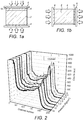
- Figures 1a and 1b show a schematic of a controlled stress system.
- the stress is applied, in this example, on a planar detector (2) and either on the contact side ( Figure 1a ) or on the edge side ( Figure 1b ).
- the detector (2) is a piezoelectric material for example of the cadmium telluride or cadmium zinc telluride type, and in an example embodiment is CdTe and is provided with a metallic contact (4) on each of two opposing faces.
- a stress is applied via rigid plates (6) (which may for example be ceramic, metallic or plastic) disposed on each of two opposing faces either on the contact side ( Figure 1a ) or on the edge side ( Figure 1b ).
- a stress is applied through a high dielectric and resistivity soft material layer (8) (such as a silicone rubber or anisotropic layer for example comprising anisotropic tapes) in order to apply a uniform stress on the whole device surface.
- a pressure gauge (10) inserted between one of the plates (6) and the high dielectric layer (8), is used to measure the applied pressure on the detector. The dielectric layer and plate are held by a clamp or a micrometer screw stage (not shown). The stress in this example is created via a controlled static pressure in the direction of the arrows.
- a stress is applied by an Al plate (6).
- a silicone rubber (8) has been used between the device surface and the Al plate in order to apply a uniform stress on the whole device surface.
- An example of the device performance under various pressures has been given on the figures 2 , 3 and 4 . In each case a controlled pressure has been applied uniformly on a planar detector and on the metallic contact side as shown the figure 1a .
- Figures 2 and 3 demonstrate the variation of the 57 Co gamma ray performance under different pressures. As we can notice and under a small pressure (250g in this case), an improvement of the detector performance in term of energy resolution (FWHM) and peak to valley (P/V) is observed. At higher pressures, a deterioration of the detector performance was noticed.
- FWHM energy resolution
- P/V peak to valley
- Figure 4 shows the leakage current at 300V of applied voltage and under various pressures. As with figures 2 and 3 , similar behaviour was noticed for the detector leakage current where it varies with the applied pressures on the detector.
- the effect of the application of a controlled stress can be to improve the detector performance, in particular once an optimised applied stress is determined. This can be explained by a variation in term of concentration and energy of the intrinsic defects leading to a better compensation and so to an improvement of the electrical field throughout the detector.
- the detailed example given does not form part of the invention, but illustrates the principles underlying the invention in the application of a controlled pressure to a planar detector.
- the same approach is used in the invention on a micropixellated detector in that a pattern of microstress having the same pitch as the detector micropixels is applied to correct and improve the electrical performance for each pixel, for example to accommodate a non-uniform semiconductor material performance.
- the detailed example given applied a controlled pressure to the face of the device (as in Figure 1a ).
- a controlled stress can also be applied on the edge side of the device (as in figure 1b ) leading to a similar effect.
Landscapes
- Physics & Mathematics (AREA)
- Health & Medical Sciences (AREA)
- Life Sciences & Earth Sciences (AREA)
- General Physics & Mathematics (AREA)
- High Energy & Nuclear Physics (AREA)
- Molecular Biology (AREA)
- Spectroscopy & Molecular Physics (AREA)
- Measurement Of Radiation (AREA)
- Engineering & Computer Science (AREA)
- Manufacturing & Machinery (AREA)
- Analysing Materials By The Use Of Radiation (AREA)
- Solid State Image Pick-Up Elements (AREA)
Description
- The invention relates to a semiconductor detector device, and to a method of operation and/ or fabrication of a semiconductor detector device. In particular the invention preferably relates to a semiconductor detector for the detection of radiation and especially for high energy physics applications, such as a detector for high energy electromagnetic radiation such as x-rays and/or gamma rays. In particular the invention preferably relates to a semiconductor detector device having a detection area defining a plurality of separately addressed regions or pixels (that is, the detector is a pixellated detector).
- Semiconductor based detector devices are widely used for the detection of radiation for a range of applications.
- There has been increased use in recent years of alternative compound semiconducting materials for semiconductor detector devices, in particular for higher energy applications. This includes for example detector devices including group II-VI semiconductors such as semiconductors of the cadmium telluride type (including for example cadmium telluride, cadmium zinc telluride (CZT), cadmium manganese telluride (CMT), mercury cadmium telluride, mercury zinc telluride and alloys thereof), and other compound semiconductors such as, for example, gallium arsenide, indium gallium arsenide, lanthanum bromide, thorium bromide. For example, bulk single crystal cadmium telluride, CZT, CMT lanthanum bromide and thorium bromide semiconductors are known to be useful of x-ray and gamma-ray detectors which have application in security screening, medical imaging and space exploration amongst other things. Cadmium mercury telluride, mercury zinc telluride, and indium gallium arsenide are useful in particular in the infra-red.
- Pixellated radiation detector structures comprising a detector material having a pixellated structure to define a plurality of discretely addressable individual elements across an area of detector material, typically to convert an area modulated incident radiation into an area modulated photoelectric response, have found increasing application in recent years. The principle is used for instance in silicon or other semiconductor based charge coupled devices (CCDs) for use in digital photography, optical and IR spectroscopy and the like, and in higher energy applications for example for X-ray and CT imaging and like applications.
For example, a detector device may be provided comprising a semiconductor detector element defining a two dimensional multiple array of small pixels (for example with a 200µm to 1mm pitch) which may be mounted to a suitable contact by means of which each pixel element may be addressed separately, for example by bump bonding to a suitable ASIC that amplifies the signal from each pixel.
Such a small pixel device can benefit from the known "small pixel effect". In a simple plane parallel device, charges distributed evenly through the thickness. In a plural small pixel device, the charge distribution tends to become much more non-linear. The small pixel effect affects how the charge signal is induced in the positive contact, and tends to produce a tighter resolution in the device. The shape of the charge experienced locally to the positive contact for each pixel is the key to controlling the small pixel effect, in particular considering the design of the contact versus thickness and the contact size versus thickness. In pixellated devices it is accepted that it is generally desirable to develop devices where the small pixel effect is exploited and enhanced.
FR2372440
In accordance with the invention in the first aspect there is provided a semiconductor radiation detector device in accordance with claim 1. - Although this aspect of the invention is not to be considered limited to a particular mechanism of operation it can be noted that a predetermined electrical field may be generated in particular via the piezoelectric effect and/ or by appropriate control of the effect of intrinsic defects. Thus, the invention at its broadest comprises a device which is inherently adapted to enable in use the generation within a micropixellated detector element of a patterned electrical field, for example by exploiting the inherent piezoelectric properties of the detector element in a controlled manner and/ or by appropriate control of the effect of intrinsic defects, so as to modify the electrical behaviour of the detector. In particular, the application of a predetermined pattern of microstress with the same pitch as the detector micropixels permits the generation of a predetermined varied electrical field and thus various electrical transports properties of electrons and holes which can modify the performance of the detector differently in these specific areas. The stress inducing element acts in use across at least a part of the surface of an area detector, and thereby selectively modifies properties thereof by generating in use a patterned variable electrical field. It may do so mechanically by direct force or pressure application to produce strain, actively in use by direct force application or passively by mechanical pre-stressing, or indirectly by otherwise creating strain within the structure, for example by inducing thermal changes that create material stresses by exploiting differential thermal expansion within a detector element or between a detector element and other device components, and may do so to generate static or dynamically varying material stresses, without departing from the principles of the invention. Rather, the key to the invention is that, however created, there may be generated during use a controlled and selective predetermined pattern of stress that generates a consequently controlled and selective predetermined patterned electrical field.
It is known in the prior art that a large number of semiconductor detector materials, in particular those fabricated from compound semiconductors, exhibit piezoelectric properties. Conventionally, the piezoelectric properties of such detector elements have been considered a potential problem. In a practical detector, any active layer of detector material must typically find itself in mechanical relationship with a variety of other layers, for example supporting substrates, housings, contact devices such as ASICs, and the like. The piezoelectric semiconductor material is typically mounted by an appropriate mounting process, for example by bump bonding. Strain induced in the semiconductor detector element, whether as a result of pre-stressing effects through the mounting, or as a result of stresses generated during use, for example mechanically, via thermal expansion effects etc, generates electrical fields in an uncontrolled manner within the device which are detrimental to its operation. - Various solutions in the prior art attempt to mitigate or accommodate these detrimental aspects of the piezoelectric properties of such detector elements. For example, an applied stress applied for example mechanically or acoustically during fabrication followed by annealing might be used to improve detector performance. Modifications might be made to the bump bonding or like mounting processes to reduce induced stresses during fabrication or use. The effects of the piezoelectric property on the function of such detector elements are known. However the prior art treats them as detrimental effects to be mitigated or accommodated, but not to be desired.
- By contrast, in accordance with the invention, this property of the detector element which was previously considered potentially detrimental and something to be avoided or dealt with by remedial action is specifically exploited by the deliberate inducing of predetermined stress patterns in use in the piezoelectric detector element to deliberately generate predetermined variable electrical field patterns therein, and thereby produce a controlled variation in performance which can thus be made beneficial to device operation by appropriate selection of predetermined stress patterns.
- A predetermined stress pattern is used to generate a desired patterned electrical field selectively to modify the device response of specific areas of the detector element, for example to mitigate local detrimental effects such as edge effects or to enhance local positive effects.
- The piezoelectric effect is specifically and deliberately induced during use, by the deliberate inducing of predetermined stress patterns, rather than being treated as something to reduce, accommodate or mitigate. Controlled stresses and pressures exploit the piezoelectric effect on the detector to improve the performance of the detector. The stresses have an impact on the electrical defects, the electrical field, and the piezoelectric effect, modifying the concentration and energy of the surface defects as well as those in the band gap, the electrical field form between the two electrodes, and the mobility-life time of the electron and holes leading to the controlled improvement of leakage current, transport properties and gamma performance of the detectors.
- Application of a controlled mechanical stress on the device (metallic contact/ interface/ semiconductor) or from the edge side of the device allows a user to control and modify the intrinsic defect concentration and/or energy leading to a better compensation of charges and thus to an improvement of electrical field form through the device. This can control and/or improve the device performance in terms of energy resolution (FWHM) and efficiency. The controlled stress can be applied on a planar detector as well as on a pixellated one.
- However in the preferred case, the detector element is a pixellated detector element, and the induced stress pattern is selectively induced at least to complement/ enhance the small pixel effect.
- In this preferred case, a detector element comprises a pixellated detector, defining (for example by appropriate arrangement of contacts, insulators etc as will be familiar) a plurality of separately addressed sub-elements in at least one direction and preferably in a two dimensional and for example square array. Pixellated detector structures are well known, and the invention is not intended to be limited to particular patterns of pixel.
- The stress inducing element is so configured as to generate a predetermined stress pattern, and consequently predetermined electrical field pattern, which is such as to complement the small pixel effect in such a pixellated device. For example, the predetermined pattern is generated on a pixel scale.
In the particular preferred case, pixels define a repeat distance or pitch in that they are evenly spaced in at least one direction, and the predetermined pattern is a repeating pattern that repeats with the same pitch as the pixel pitch. Preferably, the pixels comprise a two dimensional array, and the predetermined pattern is a repeating pattern that repeats on the same pitch as the pixel pitch in the two dimensions.
The electrical field thus generated is a field with a pixel scale pattern, and for example a pattern which repeats by pixel pitch. For example the pixels comprise a two dimensional array, and the electrical field pattern is a repeating pattern that repeats on the same pitch as the pixel pitch in the two dimensions.
Such an electrical field pattern can be used to control and modify the small pixel effect on a pixel by pixel scale. For example, a device may be produced in which the small pixel effect, and the resultant benefits of device resolution, are enhanced and/or may be used in a device to mitigate the effects of other device modifications that might otherwise be detrimental to the small pixel effect. - In the invention, the detector element has a micropixellated pattern. The stress inducing element is so configured as to generate a microstress pattern with the same repeat pitch.
The invention at its broadest lies in the provision of some form of stress inducing element to induce a pattern of microstress with the same pitch as the detector micropixels, and thereby produce the appropriate patterned electrical field via the piezoelectric effect in the piezoelectric micropixellated detector element. The invention is not limited by the particular implementation of this, or by a particular configuration of stress inducing element. - In a possible case, a stress inducing element is adapted in use to act mechanically upon the detector element to produce appropriate mechanical stress patterns therein during use. A stress inducing element that is adapted in use to act mechanically upon the detector element may do so directly or via engagement mechanically through other structures such as further active, passive or substrate layers, device housings and the like.
- In an alternative case a stress inducing element may be a part of a device structure, for example to induce a pre-stress to the device, and the invention encompasses in this regard both separate elements having such activity and the provision of an inherent pre-stress to the detector element itself, whereby the detector element itself serves also as the stress inducing element.
- Embodiments of the invention can be envisaged where the stress inducing element is so configured as to induce an inherent pre-stress in the detector element to generate the appropriate stress pattern and/or where the stress inducing element applies a deformation force dynamically during use, for example under user control. A stress pattern may be induced in uniform manner or area by area, for example under selective user control. For example, in the pixellated case, stress may be generated dynamically uniformly over a large area or pixel by pixel as required.
- It can be envisaged that a stress inducing element might comprise one or more of a substrate layer on which the detector element may be mounted with an appropriate pre-stress pattern, a substrate layer on which the detector element may be mounted, which layer is so configured as to generate an appropriate stress pattern on application of an external force from a force applicator, and a discrete force applicator configured to act selectively during use upon the detector element to generate an appropriate stress pattern.
- In one possible embodiment, the device comprises a supporting substrate mechanically engaged with the detector element in such a manner as to induce an appropriate predetermined stress pattern in use, for example being bonded thereto to induce pre-stresses generating an appropriate stress pattern and/or being structured such that the required stress pattern is inherently generated on application of an external force.
- For example, a substrate is a planar substrate with a suitably patterned surface comprising a pattern of projections and recesses, such as a combination of dimples, pins and the like, which presents a contact surface with an selectively contacts the detector element. Such a patterned surface substrate may be bonded to the detector element, for example in such a manner as to induce patterned pre-stresses and/or may be disposed to be acted upon in use by a forced applicator, for example applying pressure to an opposite surface thereof, to induce stress patterns within the detector element.
- Additionally or alternatively the detector element may be co-operatively disposed with a force applicator that mechanically engages selectively in use with the detector element to apply a force thereto and generate a patterned stress therein. Again, for example, the force applicator could comprise a shaped surface structure having a suitable patterned arrangement of projections and recesses so as to generate stress patterns of a predetermined nature when pressed against the detector element.
- Additionally or alternatively to the use a shaped surface in this manner, a force applicator substrate or a discrete force applicator may comprise a further piezoelectric element mechanically engageable with the detector element and provided with a means to selectively apply an electrical field to the substrate/ force applicator to generate a mechanical distortion therein, and thereby apply predetermined mechanical patterned stress to the detector element.
- In accordance with either of these alternatives, potentially complex mechanically produced stress patterns are possible, and in particular stress patterns are possible in which separate areas of the detector are separately controlled, and for example in the preferred case in which separate pixels are separately controlled.
- Additionally or alternatively the stress inducing element may act without mechanical engagement with the detector element otherwise to creating stress within the detector element structure. For example, differential thermal expansion between a detector element and other device components such as between a detector element and a substrate on which the detector element is mounted and/ or between layers of a detector element may be exploited in order to generate stress in use. By appropriate selection of such substrate or layers, and by provision of a means to apply controlled variations in temperature to the device during use, an additional mechanism to induce strain patterns in the detector element during use can be provided.
- For example a stress inducing element may comprise a heat source that creates thermal changes in the environment of the detector element and acts to induce stresses by exploiting differential thermal expansion within a detector element or between a detector element and other device components such as a device substrate on which the detector element is mounted, further device layers etc.
- In a possible arrangement, differential expansion coefficients and thermal effects may be used to induce stresses in one direction, and applied mechanical force may be used to induced stresses in another direction.
- In a preferred case, a force applicator is adapted to produce a static pressure in use so as to generate steady state loading conditions. In an alternative case, a force applicator may additionally be adapted to apply a dynamically varying pressure and/or to apply differential pressure to different areas of the device.
- A range of applications can be envisaged for a device in accordance with the invention, in particular in the preferred embodiment comprising those applications where a pixellated device with multiple small pixels is desirable. Suitable fields include the field of radiation detection, the field of high resolution spectroscopy, and applications where high counted rate large area detectors are required, such as for medical CT. However, the invention is not limited by particular application.
- The invention is applicable to detector elements fabricated from any material in which the piezoelectric effect can be exploited to generate a predetermined stress pattern to control the electrical behaviour of a detector element fabricated therefrom, and for example to modify the small pixel effect.
- Many compound semiconducting materials for example exhibit suitable piezoelectric properties. These include for example group II-VI semiconductors such as semiconductors of the cadmium telluride type (including for example cadmium telluride, cadmium zinc telluride (CZT), cadmium manganese telluride (CMT), mercury cadmium telluride, mercury zinc telluride and alloys thereof), and other compound semiconductors such as, for example, gallium arsenide, indium gallium arsenide, lanthanum bromide, thorium bromide. Materials making up the semiconductor element of the invention preferably include one or more piezoelectric semiconductor from the above list.
- The materials making up the semiconductor detector element are in particular preferably selected from cadmium telluride, cadmium zinc telluride (CZT), cadmium manganese telluride (CMT), germanium, lanthanum bromide, thorium bromide. Group II-VI semiconductors, and especially those listed, are particularly preferred in this regard. The materials making up the semiconductor detector element are preferably selected from cadmium telluride, cadmium zinc telluride (CZT), cadmium manganese telluride (CMT) and alloys thereof, and for example comprise crystalline Cd1-(a+b)MnaZnbTe where a + b < 1 and a and/ or b may be zero.
- A semiconductor detector element may comprise at least one layer formed as a single crystal and for example as a bulk single crystal (where bulk crystal in this context indicates a thickness of at least 500 µm, and preferably of at least 1 mm).
- In accordance with the invention in a further aspect, a method of operation of a radiation detector device comprises the steps of
claim 8. The method is in particular preferably a method of operation of the device in accordance with the first aspect of the invention, and embodies generally analogous principles, and preferred features of the method will accordingly be understood by analogy with preferred features described herein above in relation to the device of the first aspect of the invention.
In particular, the method comprises, during operation of a detector device incorporating a micropixellated detector element having at least one piezoelectric semiconductor detector layer, generating an appropriately controlled pattern of microstress with the same pitch as the detector micropixels and thereby, via the piezoelectric effect and by controlling the intrinsic defects concentration and/or energy, an appropriately controlled patterned electric field is created allowing modification of the electrical behaviour of the detector, and in particular to modify detector performance in these specific areas of the detector.
In the preferred case, the detector is a pixellated detector, in that the detector element is divided into a plurality of separately addressed sub-elements in at least one direction and preferably in a two dimensional array and the stress inducing method step comprises inducing a predetermined pattern of strain such as to generate a patterned electrical field which complements the small pixel effect in the pixellated detector in use. For example, the predetermined pattern is on a pixel scale.
In a particular preferred case, the pixels define a repeat distance or pitch in that they are evenly spaced in at least one direction, and a predetermined stress pattern is applied as a repeating pattern that repeats with the same pitch as the pixel pitch. Preferably, the pixels comprise a two dimensional array, and a predetermined stress pattern is applied as a repeating pattern that repeats on the same pitch as the pixel pitch in the two dimensions. - The electrical field thus generated is a field with a pixel scale pattern, and for example a pattern which repeats by pixel pitch. For example the pixels comprise a two dimensional array, and the electrical field pattern is a repeating pattern that repeats on the same pitch as the pixel pitch in the two dimensions.
Other preferred features of the method of the second aspect will be understood by analogy with the discussion of the device of the first aspect of the invention.
In accordance with the invention in a third aspect, a method fabrication of a radiation detector device comprises the steps of claim 13. The stress inducing element is conveniently so configured and arranged as in use to act mechanically upon the micropixellated detector element to produce appropriate mechanical pattern of microstress with the same pitch as the detector micropixels therein during use and is in a possible case an external force applicator positioned to act mechanically upon the detector element to apply a force thereto. In an alternative case a stress inducing element may be a part of a device structure, for example to induce a pre-stress to the device, and the invention encompasses in this regard both separate elements having such activity and the provision of an inherent pre-stress to the detector element itself, whereby the detector element itself serves also as the stress inducing element. - The method is in particular preferably a method of fabrication of the device in accordance with the first aspect of the invention, and embodies generally analogous principles, and preferred features of the method will accordingly be understood by analogy with preferred features described herein above in relation to the device of the first aspect of the invention and the method of the second aspect of the invention.
- The invention will now be described by way of example only with reference to the accompanying drawings in which:
-
Figure 1 is a schematic of controlled pressure system used for a planar detector with applied pressure on: a) contact/interface/SC side, b) edge side of the detector; -
Figure 2 is a graphical representation of 57Co gamma ray performance for a planar detector under different pressures applied on the contact side; -
Figure 3 is a graphical representation of Energy resolution (FWHM) and Peak to valley (P/V) for a planar detector under different pressures applied on the contact side; -
Figure 4 is a graphical representation of leakage current at V=300V for a planar detector at different pressures applied on the contact side. -
Figures 1a and 1b show a schematic of a controlled stress system. The stress is applied, in this example, on a planar detector (2) and either on the contact side (Figure 1a ) or on the edge side (Figure 1b ). The detector (2) is a piezoelectric material for example of the cadmium telluride or cadmium zinc telluride type, and in an example embodiment is CdTe and is provided with a metallic contact (4) on each of two opposing faces. - A stress is applied via rigid plates (6) (which may for example be ceramic, metallic or plastic) disposed on each of two opposing faces either on the contact side (
Figure 1a ) or on the edge side (Figure 1b ). A stress is applied through a high dielectric and resistivity soft material layer (8) (such as a silicone rubber or anisotropic layer for example comprising anisotropic tapes) in order to apply a uniform stress on the whole device surface. A pressure gauge (10), inserted between one of the plates (6) and the high dielectric layer (8), is used to measure the applied pressure on the detector. The dielectric layer and plate are held by a clamp or a micrometer screw stage (not shown). The stress in this example is created via a controlled static pressure in the direction of the arrows. - In the illustrated embodiment, as an example only, a stress is applied by an Al plate (6). A silicone rubber (8) has been used between the device surface and the Al plate in order to apply a uniform stress on the whole device surface.
An example of the device performance under various pressures has been given on thefigures 2 ,3 and 4 . In each case a controlled pressure has been applied uniformly on a planar detector and on the metallic contact side as shown thefigure 1a . -
Figures 2 and3 demonstrate the variation of the 57Co gamma ray performance under different pressures. As we can notice and under a small pressure (250g in this case), an improvement of the detector performance in term of energy resolution (FWHM) and peak to valley (P/V) is observed. At higher pressures, a deterioration of the detector performance was noticed. -
Figure 4 shows the leakage current at 300V of applied voltage and under various pressures. As withfigures 2 and3 , similar behaviour was noticed for the detector leakage current where it varies with the applied pressures on the detector. - It can be seen from the above example for a planar detector that the effect of the application of a controlled stress can be to improve the detector performance, in particular once an optimised applied stress is determined. This can be explained by a variation in term of concentration and energy of the intrinsic defects leading to a better compensation and so to an improvement of the electrical field throughout the detector.
- The detailed example given does not form part of the invention, but illustrates the principles underlying the invention in the application of a controlled pressure to a planar detector. The same approach is used in the invention on a micropixellated detector in that a pattern of microstress having the same pitch as the detector micropixels is applied to correct and improve the electrical performance for each pixel, for example to accommodate a non-uniform semiconductor material performance.
The detailed example given applied a controlled pressure to the face of the device (as inFigure 1a ). Alternatively a controlled stress can also be applied on the edge side of the device (as infigure 1b ) leading to a similar effect.
Claims (15)
- A semiconductor radiation detector device comprising:a detector element (2) comprising at least one active detector layer of piezoelectric semiconductor material;a stress inducing element (6) arranged to act in use on the detector element to generate therein a predetermined pattern of stress, and consequently a predetermined electrical field;characterised in that the detector element is a pixellated detector element and has a micropixellated pattern of a predetermined repeat pitch, and the stress inducing element is so configured as to generate a microstress pattern with the same repeat pitch.
- A device in accordance with claim 1 wherein the stress inducing element (6) is adapted in use to act mechanically upon the detector element to induce an inherent pre-stress in the detector element to induce a mechanical stress pattern therein in use.
- A device in accordance with any preceding claim wherein the stress inducing element comprises a supporting substrate mechanically engaged with the detector element in such a manner as to induce a mechanical stress pattern therein.
- A device in accordance with any preceding claim wherein the stress inducing element (6) includes a force applicator co-operatively disposed with the detector element so as to mechanically engage selectively in use with the detector element (2) to apply a force thereto and generate a mechanical stress pattern therein, wherein the force applicator comprises a shaped surface structure having a suitable patterned arrangement of projections and recesses so as to generate stress patterns of a predetermined nature when pressed against the detector element.
- A device in accordance with any preceding claim wherein the stress inducing element (6) is adapted to induce predetermined variable stress patterns in use in the piezoelectric detector element (2) to deliberately generate predetermined variable electrical field patterns therein.
- A device in accordance with any preceding claim wherein the stress inducing element (6) is adapted to induce a stress pattern such as at least to complement/ enhance the small pixel effect.
- A device in accordance with any preceding claim wherein the detector element (2) comprises a compound semiconductor comprising crystalline Cd1-(a+b)MnaZnbTe where a + b < 1 and a and/ or b may be zero.
- A method of operation of a radiation detector device comprising the steps of:providing a detector device comprising at least one detector element (2) having at least one active detector layer of a piezoelectric semiconductor material;operating the detector element whilst inducing therein a predetermined stress pattern, and consequently inducing therein a predetermined pattern of electrical field, characterised in that the detector is a pixellated detector having a micropixellated pattern of a predetermined repeat pitch and the predetermined pattern is generated on a pixel scale as a microstress pattern with the same repeat pitch.
- The method of claim 8 wherein the step of inducing a predetermined stress pattern comprises causing a stress inducing element (6) to act mechanically upon the detector element to produce a mechanical stress pattern therein in such manner as to induce an inherent pre-stress therein to produce a mechanical stress pattern therein.
- The method of one of claims 8 or 9 wherein the step of inducing a predetermined stress pattern comprises disposing the detector on a supporting substrate mechanically engaged with the detector element in such a manner as to induce a mechanical stress pattern therein.
- The method of one of claims 8 to 10 comprising, during operation of a detector device incorporating a detector element having at least one piezoelectric semiconductor detector layer, generating an appropriately controlled stress pattern and thereby an appropriately controlled patterned electric field to modify the electrical behaviour of the detector and to modify detector performance in specific areas of the detector.
- The method of one of claims 8 to 11 comprising inducing a predetermined pattern of strain such as to generate a patterned electrical field which complements the small pixel effect in the pixellated detector.
- A method of fabrication of a radiation detector device comprising the steps of:providing a detector device comprising at least one detector element (2) having at least one active detector layer of a piezoelectric semiconductor material;associating with the detector element a stress inducing element (6) arranged to act in use on the detector element to generate therein a predetermined pattern of stress, and consequently a predetermined electrical field; characterised in that the detector is a pixellated detector having a micropixellated pattern of a predetermined repeat pitch and the stress inducing element is arranged to act in use on the detector element to generate a predetermined pattern on a pixel scale as a microstress pattern with the same repeat pitch.
- The method of claim 13 wherein the step of associating a stress inducing element with the detector element comprises providing a stress inducing element (6) adapted to act mechanically upon the detector element (2) in such manner as to induce an inherent pre-stress therein to produce a mechanical stress pattern therein.
- The method of one of claims 13 or 14 wherein the step of associating a stress inducing element with the detector element comprises disposing the detector on a supporting substrate mechanically engaged with the detector element in such a manner as to induce a mechanical stress pattern therein.
Applications Claiming Priority (2)
| Application Number | Priority Date | Filing Date | Title |
|---|---|---|---|
| GBGB1214567.8A GB201214567D0 (en) | 2012-08-15 | 2012-08-15 | Detector and method of operation |
| PCT/GB2013/052154 WO2014027192A1 (en) | 2012-08-15 | 2013-08-14 | Stressed semiconductor detector with piezoelectrical component |
Publications (2)
| Publication Number | Publication Date |
|---|---|
| EP2885655A1 EP2885655A1 (en) | 2015-06-24 |
| EP2885655B1 true EP2885655B1 (en) | 2018-10-03 |
Family
ID=46981566
Family Applications (1)
| Application Number | Title | Priority Date | Filing Date |
|---|---|---|---|
| EP13750919.6A Active EP2885655B1 (en) | 2012-08-15 | 2013-08-14 | Stressed semiconductor detector with piezoelectrical component |
Country Status (5)
| Country | Link |
|---|---|
| US (1) | US9293628B2 (en) |
| EP (1) | EP2885655B1 (en) |
| JP (1) | JP6111333B2 (en) |
| GB (1) | GB201214567D0 (en) |
| WO (1) | WO2014027192A1 (en) |
Families Citing this family (1)
| Publication number | Priority date | Publication date | Assignee | Title |
|---|---|---|---|---|
| US11738369B2 (en) * | 2020-02-17 | 2023-08-29 | GE Precision Healthcare LLC | Capactive micromachined transducer having a high contact resistance part |
Family Cites Families (18)
| Publication number | Priority date | Publication date | Assignee | Title |
|---|---|---|---|---|
| GB808630A (en) * | 1956-04-20 | 1959-02-11 | Plessey Co Ltd | A charging device for electrometers |
| US3743953A (en) * | 1971-06-10 | 1973-07-03 | Gte Laboratories Inc | Surface wave acoustic parametric amplifier |
| DE2741865A1 (en) * | 1976-09-22 | 1978-03-23 | Emi Ltd | ARRANGEMENT FOR DETECTING PENETRATING RADIATION |
| GB8913450D0 (en) * | 1989-06-12 | 1989-08-02 | Philips Electronic Associated | Electrical device manufacture,particularly infrared detector arrays |
| JPH0461173A (en) * | 1990-06-22 | 1992-02-27 | Nikko Kyodo Co Ltd | Manufacture of semiconductor radiation detector |
| GB2289983B (en) | 1994-06-01 | 1996-10-16 | Simage Oy | Imaging devices,systems and methods |
| US6114698A (en) * | 1997-01-31 | 2000-09-05 | The United States Of America As Represented By The Secretary Of Commerce | Domain engineered ferroelectric optical radiation detector |
| US6376971B1 (en) | 1997-02-07 | 2002-04-23 | Sri International | Electroactive polymer electrodes |
| WO2000040938A1 (en) * | 1999-01-08 | 2000-07-13 | Sarnoff Corporation | Optical detectors using nulling for high linearity and large dynamic range |
| US6359281B1 (en) | 1999-05-06 | 2002-03-19 | Siemens Medical Systems, Inc. | High voltage distribution system for solid state scintillation detectors and gamma camera system incorporating the same |
| JP3512379B2 (en) * | 2000-09-20 | 2004-03-29 | 日本碍子株式会社 | Piezoelectric element and method of manufacturing the same |
| US6645787B2 (en) * | 2002-01-22 | 2003-11-11 | Technion Research And Development Foundation Ltd. | Gamma ray detector |
| US7223981B1 (en) | 2002-12-04 | 2007-05-29 | Aguila Technologies Inc. | Gamma ray detector modules |
| AT500829B1 (en) * | 2004-10-07 | 2007-03-15 | Piezocryst Ges Fuer Piezoelek | SENSOR ELEMENT WITH AT LEAST ONE MEASURING ELEMENT WHICH HAS PIEZOELECTRIC AND PYROELECTRIC PROPERTIES |
| US7212604B2 (en) * | 2005-06-29 | 2007-05-01 | General Electric Company | Multi-layer direct conversion computed tomography detector module |
| JP4777077B2 (en) | 2006-01-20 | 2011-09-21 | 富士フイルム株式会社 | Functional element |
| GB0712618D0 (en) * | 2007-06-29 | 2007-08-08 | Durham Scient Crystals Ltd | Semiconductor device structure and method of manufacture thereof |
| GB0908583D0 (en) | 2009-05-19 | 2009-06-24 | Durham Scient Crystals Ltd | Semiconductor device contacts |
-
2012
- 2012-08-15 GB GBGB1214567.8A patent/GB201214567D0/en not_active Ceased
-
2013
- 2013-08-14 US US14/420,627 patent/US9293628B2/en active Active
- 2013-08-14 JP JP2015527024A patent/JP6111333B2/en not_active Expired - Fee Related
- 2013-08-14 WO PCT/GB2013/052154 patent/WO2014027192A1/en not_active Ceased
- 2013-08-14 EP EP13750919.6A patent/EP2885655B1/en active Active
Non-Patent Citations (1)
| Title |
|---|
| None * |
Also Published As
| Publication number | Publication date |
|---|---|
| JP2015531862A (en) | 2015-11-05 |
| EP2885655A1 (en) | 2015-06-24 |
| JP6111333B2 (en) | 2017-04-05 |
| US20150194560A1 (en) | 2015-07-09 |
| WO2014027192A1 (en) | 2014-02-20 |
| GB201214567D0 (en) | 2012-09-26 |
| US9293628B2 (en) | 2016-03-22 |
Similar Documents
| Publication | Publication Date | Title |
|---|---|---|
| EP0543951B1 (en) | Solid state electromagnetic radiation detector | |
| US7301155B2 (en) | Radiation detector and radiation imaging apparatus and method for producing radiation detector | |
| JP3430040B2 (en) | Two-dimensional image detector and manufacturing method thereof | |
| JP7453215B2 (en) | Multi-piece single layer radiation detector | |
| JP2013142578A (en) | Radiation detector | |
| JPH09275223A (en) | Semiconductor radiation detector | |
| EP2244294A1 (en) | Method for manufacturing radiation detector, radiation detector, and radiation image pickup device | |
| US11056597B2 (en) | Photoelectric conversion device, photosensor, power generation device, and photoelectric conversion method | |
| US20020131011A1 (en) | Active matrix substrate, electromagnetic detector, and liquid crystal display apparatus | |
| Liu et al. | Radiation-hardened and flexible Pb (Zr0. 53Ti0. 47) O3 piezoelectric sensor for structural health monitoring | |
| US20080099869A1 (en) | Two-Dimensional Image Detecting Apparatus and Method for Manufacturing the Same | |
| JP4066972B2 (en) | Flat panel radiation detector | |
| US9293628B2 (en) | Stressed semiconductor detector with piezoelectrical component | |
| CN102460215B (en) | Method of manufacturing radiation detector, radiation detector, and radiographic device | |
| CN101390213B (en) | Radiation detector | |
| US10374110B2 (en) | Transducing apparatus and method for providing such apparatus | |
| US20090065680A1 (en) | Image detecting device | |
| US6949749B2 (en) | Electromagnetic imaging apparatus and manufacturing method therefor | |
| JP5343550B2 (en) | Manufacturing method of radiation detector | |
| US8324582B2 (en) | Direct conversion X-ray imaging device with strip electrodes | |
| JP3978971B2 (en) | Two-dimensional image detector and manufacturing method thereof | |
| WO2013080251A1 (en) | Radiation detector | |
| JP5299190B2 (en) | Manufacturing method of optical matrix device | |
| JP2004209117A (en) | Radiation detecting instrument, and its production method | |
| JP2000294759A (en) | 2D image detector |
Legal Events
| Date | Code | Title | Description |
|---|---|---|---|
| PUAI | Public reference made under article 153(3) epc to a published international application that has entered the european phase |
Free format text: ORIGINAL CODE: 0009012 |
|
| 17P | Request for examination filed |
Effective date: 20150205 |
|
| AK | Designated contracting states |
Kind code of ref document: A1 Designated state(s): AL AT BE BG CH CY CZ DE DK EE ES FI FR GB GR HR HU IE IS IT LI LT LU LV MC MK MT NL NO PL PT RO RS SE SI SK SM TR |
|
| AX | Request for extension of the european patent |
Extension state: BA ME |
|
| DAX | Request for extension of the european patent (deleted) | ||
| GRAP | Despatch of communication of intention to grant a patent |
Free format text: ORIGINAL CODE: EPIDOSNIGR1 |
|
| STAA | Information on the status of an ep patent application or granted ep patent |
Free format text: STATUS: GRANT OF PATENT IS INTENDED |
|
| INTG | Intention to grant announced |
Effective date: 20180221 |
|
| GRAS | Grant fee paid |
Free format text: ORIGINAL CODE: EPIDOSNIGR3 |
|
| GRAJ | Information related to disapproval of communication of intention to grant by the applicant or resumption of examination proceedings by the epo deleted |
Free format text: ORIGINAL CODE: EPIDOSDIGR1 |
|
| GRAL | Information related to payment of fee for publishing/printing deleted |
Free format text: ORIGINAL CODE: EPIDOSDIGR3 |
|
| STAA | Information on the status of an ep patent application or granted ep patent |
Free format text: STATUS: REQUEST FOR EXAMINATION WAS MADE |
|
| GRAR | Information related to intention to grant a patent recorded |
Free format text: ORIGINAL CODE: EPIDOSNIGR71 |
|
| STAA | Information on the status of an ep patent application or granted ep patent |
Free format text: STATUS: GRANT OF PATENT IS INTENDED |
|
| INTC | Intention to grant announced (deleted) | ||
| INTG | Intention to grant announced |
Effective date: 20180702 |
|
| GRAA | (expected) grant |
Free format text: ORIGINAL CODE: 0009210 |
|
| STAA | Information on the status of an ep patent application or granted ep patent |
Free format text: STATUS: THE PATENT HAS BEEN GRANTED |
|
| AK | Designated contracting states |
Kind code of ref document: B1 Designated state(s): AL AT BE BG CH CY CZ DE DK EE ES FI FR GB GR HR HU IE IS IT LI LT LU LV MC MK MT NL NO PL PT RO RS SE SI SK SM TR |
|
| REG | Reference to a national code |
Ref country code: GB Ref legal event code: FG4D |
|
| REG | Reference to a national code |
Ref country code: CH Ref legal event code: EP Ref country code: AT Ref legal event code: REF Ref document number: 1049221 Country of ref document: AT Kind code of ref document: T Effective date: 20181015 |
|
| REG | Reference to a national code |
Ref country code: IE Ref legal event code: FG4D Ref country code: DE Ref legal event code: R096 Ref document number: 602013044500 Country of ref document: DE |
|
| REG | Reference to a national code |
Ref country code: NL Ref legal event code: MP Effective date: 20181003 |
|
| REG | Reference to a national code |
Ref country code: LT Ref legal event code: MG4D |
|
| REG | Reference to a national code |
Ref country code: AT Ref legal event code: MK05 Ref document number: 1049221 Country of ref document: AT Kind code of ref document: T Effective date: 20181003 |
|
| PG25 | Lapsed in a contracting state [announced via postgrant information from national office to epo] |
Ref country code: NL Free format text: LAPSE BECAUSE OF FAILURE TO SUBMIT A TRANSLATION OF THE DESCRIPTION OR TO PAY THE FEE WITHIN THE PRESCRIBED TIME-LIMIT Effective date: 20181003 |
|
| PG25 | Lapsed in a contracting state [announced via postgrant information from national office to epo] |
Ref country code: HR Free format text: LAPSE BECAUSE OF FAILURE TO SUBMIT A TRANSLATION OF THE DESCRIPTION OR TO PAY THE FEE WITHIN THE PRESCRIBED TIME-LIMIT Effective date: 20181003 Ref country code: PL Free format text: LAPSE BECAUSE OF FAILURE TO SUBMIT A TRANSLATION OF THE DESCRIPTION OR TO PAY THE FEE WITHIN THE PRESCRIBED TIME-LIMIT Effective date: 20181003 Ref country code: NO Free format text: LAPSE BECAUSE OF FAILURE TO SUBMIT A TRANSLATION OF THE DESCRIPTION OR TO PAY THE FEE WITHIN THE PRESCRIBED TIME-LIMIT Effective date: 20190103 Ref country code: BG Free format text: LAPSE BECAUSE OF FAILURE TO SUBMIT A TRANSLATION OF THE DESCRIPTION OR TO PAY THE FEE WITHIN THE PRESCRIBED TIME-LIMIT Effective date: 20190103 Ref country code: AT Free format text: LAPSE BECAUSE OF FAILURE TO SUBMIT A TRANSLATION OF THE DESCRIPTION OR TO PAY THE FEE WITHIN THE PRESCRIBED TIME-LIMIT Effective date: 20181003 Ref country code: FI Free format text: LAPSE BECAUSE OF FAILURE TO SUBMIT A TRANSLATION OF THE DESCRIPTION OR TO PAY THE FEE WITHIN THE PRESCRIBED TIME-LIMIT Effective date: 20181003 Ref country code: LV Free format text: LAPSE BECAUSE OF FAILURE TO SUBMIT A TRANSLATION OF THE DESCRIPTION OR TO PAY THE FEE WITHIN THE PRESCRIBED TIME-LIMIT Effective date: 20181003 Ref country code: ES Free format text: LAPSE BECAUSE OF FAILURE TO SUBMIT A TRANSLATION OF THE DESCRIPTION OR TO PAY THE FEE WITHIN THE PRESCRIBED TIME-LIMIT Effective date: 20181003 Ref country code: IS Free format text: LAPSE BECAUSE OF FAILURE TO SUBMIT A TRANSLATION OF THE DESCRIPTION OR TO PAY THE FEE WITHIN THE PRESCRIBED TIME-LIMIT Effective date: 20190203 Ref country code: LT Free format text: LAPSE BECAUSE OF FAILURE TO SUBMIT A TRANSLATION OF THE DESCRIPTION OR TO PAY THE FEE WITHIN THE PRESCRIBED TIME-LIMIT Effective date: 20181003 Ref country code: CZ Free format text: LAPSE BECAUSE OF FAILURE TO SUBMIT A TRANSLATION OF THE DESCRIPTION OR TO PAY THE FEE WITHIN THE PRESCRIBED TIME-LIMIT Effective date: 20181003 |
|
| PG25 | Lapsed in a contracting state [announced via postgrant information from national office to epo] |
Ref country code: GR Free format text: LAPSE BECAUSE OF FAILURE TO SUBMIT A TRANSLATION OF THE DESCRIPTION OR TO PAY THE FEE WITHIN THE PRESCRIBED TIME-LIMIT Effective date: 20190104 Ref country code: PT Free format text: LAPSE BECAUSE OF FAILURE TO SUBMIT A TRANSLATION OF THE DESCRIPTION OR TO PAY THE FEE WITHIN THE PRESCRIBED TIME-LIMIT Effective date: 20190203 Ref country code: RS Free format text: LAPSE BECAUSE OF FAILURE TO SUBMIT A TRANSLATION OF THE DESCRIPTION OR TO PAY THE FEE WITHIN THE PRESCRIBED TIME-LIMIT Effective date: 20181003 Ref country code: SE Free format text: LAPSE BECAUSE OF FAILURE TO SUBMIT A TRANSLATION OF THE DESCRIPTION OR TO PAY THE FEE WITHIN THE PRESCRIBED TIME-LIMIT Effective date: 20181003 Ref country code: AL Free format text: LAPSE BECAUSE OF FAILURE TO SUBMIT A TRANSLATION OF THE DESCRIPTION OR TO PAY THE FEE WITHIN THE PRESCRIBED TIME-LIMIT Effective date: 20181003 |
|
| REG | Reference to a national code |
Ref country code: DE Ref legal event code: R097 Ref document number: 602013044500 Country of ref document: DE |
|
| PG25 | Lapsed in a contracting state [announced via postgrant information from national office to epo] |
Ref country code: DK Free format text: LAPSE BECAUSE OF FAILURE TO SUBMIT A TRANSLATION OF THE DESCRIPTION OR TO PAY THE FEE WITHIN THE PRESCRIBED TIME-LIMIT Effective date: 20181003 Ref country code: IT Free format text: LAPSE BECAUSE OF FAILURE TO SUBMIT A TRANSLATION OF THE DESCRIPTION OR TO PAY THE FEE WITHIN THE PRESCRIBED TIME-LIMIT Effective date: 20181003 |
|
| PLBE | No opposition filed within time limit |
Free format text: ORIGINAL CODE: 0009261 |
|
| STAA | Information on the status of an ep patent application or granted ep patent |
Free format text: STATUS: NO OPPOSITION FILED WITHIN TIME LIMIT |
|
| PG25 | Lapsed in a contracting state [announced via postgrant information from national office to epo] |
Ref country code: SK Free format text: LAPSE BECAUSE OF FAILURE TO SUBMIT A TRANSLATION OF THE DESCRIPTION OR TO PAY THE FEE WITHIN THE PRESCRIBED TIME-LIMIT Effective date: 20181003 Ref country code: SM Free format text: LAPSE BECAUSE OF FAILURE TO SUBMIT A TRANSLATION OF THE DESCRIPTION OR TO PAY THE FEE WITHIN THE PRESCRIBED TIME-LIMIT Effective date: 20181003 Ref country code: EE Free format text: LAPSE BECAUSE OF FAILURE TO SUBMIT A TRANSLATION OF THE DESCRIPTION OR TO PAY THE FEE WITHIN THE PRESCRIBED TIME-LIMIT Effective date: 20181003 Ref country code: RO Free format text: LAPSE BECAUSE OF FAILURE TO SUBMIT A TRANSLATION OF THE DESCRIPTION OR TO PAY THE FEE WITHIN THE PRESCRIBED TIME-LIMIT Effective date: 20181003 |
|
| 26N | No opposition filed |
Effective date: 20190704 |
|
| PG25 | Lapsed in a contracting state [announced via postgrant information from national office to epo] |
Ref country code: SI Free format text: LAPSE BECAUSE OF FAILURE TO SUBMIT A TRANSLATION OF THE DESCRIPTION OR TO PAY THE FEE WITHIN THE PRESCRIBED TIME-LIMIT Effective date: 20181003 |
|
| PG25 | Lapsed in a contracting state [announced via postgrant information from national office to epo] |
Ref country code: TR Free format text: LAPSE BECAUSE OF FAILURE TO SUBMIT A TRANSLATION OF THE DESCRIPTION OR TO PAY THE FEE WITHIN THE PRESCRIBED TIME-LIMIT Effective date: 20181003 |
|
| PG25 | Lapsed in a contracting state [announced via postgrant information from national office to epo] |
Ref country code: CH Free format text: LAPSE BECAUSE OF NON-PAYMENT OF DUE FEES Effective date: 20190831 Ref country code: LU Free format text: LAPSE BECAUSE OF NON-PAYMENT OF DUE FEES Effective date: 20190814 Ref country code: LI Free format text: LAPSE BECAUSE OF NON-PAYMENT OF DUE FEES Effective date: 20190831 Ref country code: MC Free format text: LAPSE BECAUSE OF FAILURE TO SUBMIT A TRANSLATION OF THE DESCRIPTION OR TO PAY THE FEE WITHIN THE PRESCRIBED TIME-LIMIT Effective date: 20181003 |
|
| REG | Reference to a national code |
Ref country code: BE Ref legal event code: MM Effective date: 20190831 |
|
| PG25 | Lapsed in a contracting state [announced via postgrant information from national office to epo] |
Ref country code: IE Free format text: LAPSE BECAUSE OF NON-PAYMENT OF DUE FEES Effective date: 20190814 |
|
| PG25 | Lapsed in a contracting state [announced via postgrant information from national office to epo] |
Ref country code: BE Free format text: LAPSE BECAUSE OF NON-PAYMENT OF DUE FEES Effective date: 20190831 |
|
| PG25 | Lapsed in a contracting state [announced via postgrant information from national office to epo] |
Ref country code: CY Free format text: LAPSE BECAUSE OF FAILURE TO SUBMIT A TRANSLATION OF THE DESCRIPTION OR TO PAY THE FEE WITHIN THE PRESCRIBED TIME-LIMIT Effective date: 20181003 |
|
| PG25 | Lapsed in a contracting state [announced via postgrant information from national office to epo] |
Ref country code: HU Free format text: LAPSE BECAUSE OF FAILURE TO SUBMIT A TRANSLATION OF THE DESCRIPTION OR TO PAY THE FEE WITHIN THE PRESCRIBED TIME-LIMIT; INVALID AB INITIO Effective date: 20130814 Ref country code: MT Free format text: LAPSE BECAUSE OF FAILURE TO SUBMIT A TRANSLATION OF THE DESCRIPTION OR TO PAY THE FEE WITHIN THE PRESCRIBED TIME-LIMIT Effective date: 20181003 |
|
| PG25 | Lapsed in a contracting state [announced via postgrant information from national office to epo] |
Ref country code: MK Free format text: LAPSE BECAUSE OF FAILURE TO SUBMIT A TRANSLATION OF THE DESCRIPTION OR TO PAY THE FEE WITHIN THE PRESCRIBED TIME-LIMIT Effective date: 20181003 |
|
| PGFP | Annual fee paid to national office [announced via postgrant information from national office to epo] |
Ref country code: DE Payment date: 20250828 Year of fee payment: 13 |
|
| PGFP | Annual fee paid to national office [announced via postgrant information from national office to epo] |
Ref country code: GB Payment date: 20250829 Year of fee payment: 13 |
|
| PGFP | Annual fee paid to national office [announced via postgrant information from national office to epo] |
Ref country code: FR Payment date: 20250827 Year of fee payment: 13 |