EP2884542A2 - Integrated circuit device with power gating switch in back end of line - Google Patents
Integrated circuit device with power gating switch in back end of line Download PDFInfo
- Publication number
- EP2884542A2 EP2884542A2 EP14191497.8A EP14191497A EP2884542A2 EP 2884542 A2 EP2884542 A2 EP 2884542A2 EP 14191497 A EP14191497 A EP 14191497A EP 2884542 A2 EP2884542 A2 EP 2884542A2
- Authority
- EP
- European Patent Office
- Prior art keywords
- layer
- power gating
- source
- integrated circuit
- metal
- Prior art date
- Legal status (The legal status is an assumption and is not a legal conclusion. Google has not performed a legal analysis and makes no representation as to the accuracy of the status listed.)
- Withdrawn
Links
Images




Classifications
-
- H—ELECTRICITY
- H10—SEMICONDUCTOR DEVICES; ELECTRIC SOLID-STATE DEVICES NOT OTHERWISE PROVIDED FOR
- H10D—INORGANIC ELECTRIC SEMICONDUCTOR DEVICES
- H10D62/00—Semiconductor bodies, or regions thereof, of devices having potential barriers
-
- H—ELECTRICITY
- H10—SEMICONDUCTOR DEVICES; ELECTRIC SOLID-STATE DEVICES NOT OTHERWISE PROVIDED FOR
- H10D—INORGANIC ELECTRIC SEMICONDUCTOR DEVICES
- H10D30/00—Field-effect transistors [FET]
- H10D30/60—Insulated-gate field-effect transistors [IGFET]
- H10D30/67—Thin-film transistors [TFT]
- H10D30/674—Thin-film transistors [TFT] characterised by the active materials
- H10D30/6755—Oxide semiconductors, e.g. zinc oxide, copper aluminium oxide or cadmium stannate
-
- H—ELECTRICITY
- H03—ELECTRONIC CIRCUITRY
- H03K—PULSE TECHNIQUE
- H03K17/00—Electronic switching or gating, i.e. not by contact-making and –breaking
- H03K17/51—Electronic switching or gating, i.e. not by contact-making and –breaking characterised by the components used
- H03K17/56—Electronic switching or gating, i.e. not by contact-making and –breaking characterised by the components used by the use, as active elements, of semiconductor devices
- H03K17/687—Electronic switching or gating, i.e. not by contact-making and –breaking characterised by the components used by the use, as active elements, of semiconductor devices the devices being field-effect transistors
-
- H—ELECTRICITY
- H10—SEMICONDUCTOR DEVICES; ELECTRIC SOLID-STATE DEVICES NOT OTHERWISE PROVIDED FOR
- H10D—INORGANIC ELECTRIC SEMICONDUCTOR DEVICES
- H10D30/00—Field-effect transistors [FET]
- H10D30/60—Insulated-gate field-effect transistors [IGFET]
-
- H—ELECTRICITY
- H10—SEMICONDUCTOR DEVICES; ELECTRIC SOLID-STATE DEVICES NOT OTHERWISE PROVIDED FOR
- H10D—INORGANIC ELECTRIC SEMICONDUCTOR DEVICES
- H10D86/00—Integrated devices formed in or on insulating or conducting substrates, e.g. formed in silicon-on-insulator [SOI] substrates or on stainless steel or glass substrates
- H10D86/40—Integrated devices formed in or on insulating or conducting substrates, e.g. formed in silicon-on-insulator [SOI] substrates or on stainless steel or glass substrates characterised by multiple TFTs
- H10D86/411—Integrated devices formed in or on insulating or conducting substrates, e.g. formed in silicon-on-insulator [SOI] substrates or on stainless steel or glass substrates characterised by multiple TFTs characterised by materials, geometry or structure of the substrates
-
- H—ELECTRICITY
- H10—SEMICONDUCTOR DEVICES; ELECTRIC SOLID-STATE DEVICES NOT OTHERWISE PROVIDED FOR
- H10D—INORGANIC ELECTRIC SEMICONDUCTOR DEVICES
- H10D86/00—Integrated devices formed in or on insulating or conducting substrates, e.g. formed in silicon-on-insulator [SOI] substrates or on stainless steel or glass substrates
- H10D86/40—Integrated devices formed in or on insulating or conducting substrates, e.g. formed in silicon-on-insulator [SOI] substrates or on stainless steel or glass substrates characterised by multiple TFTs
- H10D86/421—Integrated devices formed in or on insulating or conducting substrates, e.g. formed in silicon-on-insulator [SOI] substrates or on stainless steel or glass substrates characterised by multiple TFTs having a particular composition, shape or crystalline structure of the active layer
- H10D86/423—Integrated devices formed in or on insulating or conducting substrates, e.g. formed in silicon-on-insulator [SOI] substrates or on stainless steel or glass substrates characterised by multiple TFTs having a particular composition, shape or crystalline structure of the active layer comprising semiconductor materials not belonging to the Group IV, e.g. InGaZnO
-
- H—ELECTRICITY
- H10—SEMICONDUCTOR DEVICES; ELECTRIC SOLID-STATE DEVICES NOT OTHERWISE PROVIDED FOR
- H10D—INORGANIC ELECTRIC SEMICONDUCTOR DEVICES
- H10D86/00—Integrated devices formed in or on insulating or conducting substrates, e.g. formed in silicon-on-insulator [SOI] substrates or on stainless steel or glass substrates
- H10D86/40—Integrated devices formed in or on insulating or conducting substrates, e.g. formed in silicon-on-insulator [SOI] substrates or on stainless steel or glass substrates characterised by multiple TFTs
- H10D86/441—Interconnections, e.g. scanning lines
-
- H—ELECTRICITY
- H10—SEMICONDUCTOR DEVICES; ELECTRIC SOLID-STATE DEVICES NOT OTHERWISE PROVIDED FOR
- H10D—INORGANIC ELECTRIC SEMICONDUCTOR DEVICES
- H10D86/00—Integrated devices formed in or on insulating or conducting substrates, e.g. formed in silicon-on-insulator [SOI] substrates or on stainless steel or glass substrates
- H10D86/40—Integrated devices formed in or on insulating or conducting substrates, e.g. formed in silicon-on-insulator [SOI] substrates or on stainless steel or glass substrates characterised by multiple TFTs
- H10D86/60—Integrated devices formed in or on insulating or conducting substrates, e.g. formed in silicon-on-insulator [SOI] substrates or on stainless steel or glass substrates characterised by multiple TFTs wherein the TFTs are in active matrices
-
- H—ELECTRICITY
- H10—SEMICONDUCTOR DEVICES; ELECTRIC SOLID-STATE DEVICES NOT OTHERWISE PROVIDED FOR
- H10W—GENERIC PACKAGES, INTERCONNECTIONS, CONNECTORS OR OTHER CONSTRUCTIONAL DETAILS OF DEVICES COVERED BY CLASS H10
- H10W20/00—Interconnections in chips, wafers or substrates
- H10W20/40—Interconnections external to wafers or substrates, e.g. back-end-of-line [BEOL] metallisations or vias connecting to gate electrodes
- H10W20/49—Adaptable interconnections, e.g. fuses or antifuses
-
- H—ELECTRICITY
- H10—SEMICONDUCTOR DEVICES; ELECTRIC SOLID-STATE DEVICES NOT OTHERWISE PROVIDED FOR
- H10W—GENERIC PACKAGES, INTERCONNECTIONS, CONNECTORS OR OTHER CONSTRUCTIONAL DETAILS OF DEVICES COVERED BY CLASS H10
- H10W20/00—Interconnections in chips, wafers or substrates
- H10W20/40—Interconnections external to wafers or substrates, e.g. back-end-of-line [BEOL] metallisations or vias connecting to gate electrodes
- H10W20/41—Interconnections external to wafers or substrates, e.g. back-end-of-line [BEOL] metallisations or vias connecting to gate electrodes characterised by their conductive parts
- H10W20/425—Barrier, adhesion or liner layers
-
- H—ELECTRICITY
- H10—SEMICONDUCTOR DEVICES; ELECTRIC SOLID-STATE DEVICES NOT OTHERWISE PROVIDED FOR
- H10W—GENERIC PACKAGES, INTERCONNECTIONS, CONNECTORS OR OTHER CONSTRUCTIONAL DETAILS OF DEVICES COVERED BY CLASS H10
- H10W20/00—Interconnections in chips, wafers or substrates
- H10W20/40—Interconnections external to wafers or substrates, e.g. back-end-of-line [BEOL] metallisations or vias connecting to gate electrodes
- H10W20/41—Interconnections external to wafers or substrates, e.g. back-end-of-line [BEOL] metallisations or vias connecting to gate electrodes characterised by their conductive parts
- H10W20/427—Power or ground buses
-
- H—ELECTRICITY
- H10—SEMICONDUCTOR DEVICES; ELECTRIC SOLID-STATE DEVICES NOT OTHERWISE PROVIDED FOR
- H10W—GENERIC PACKAGES, INTERCONNECTIONS, CONNECTORS OR OTHER CONSTRUCTIONAL DETAILS OF DEVICES COVERED BY CLASS H10
- H10W20/00—Interconnections in chips, wafers or substrates
- H10W20/40—Interconnections external to wafers or substrates, e.g. back-end-of-line [BEOL] metallisations or vias connecting to gate electrodes
- H10W20/45—Interconnections external to wafers or substrates, e.g. back-end-of-line [BEOL] metallisations or vias connecting to gate electrodes characterised by their insulating parts
- H10W20/47—Interconnections external to wafers or substrates, e.g. back-end-of-line [BEOL] metallisations or vias connecting to gate electrodes characterised by their insulating parts comprising two or more dielectric layers having different properties, e.g. different dielectric constants
-
- Y—GENERAL TAGGING OF NEW TECHNOLOGICAL DEVELOPMENTS; GENERAL TAGGING OF CROSS-SECTIONAL TECHNOLOGIES SPANNING OVER SEVERAL SECTIONS OF THE IPC; TECHNICAL SUBJECTS COVERED BY FORMER USPC CROSS-REFERENCE ART COLLECTIONS [XRACs] AND DIGESTS
- Y10—TECHNICAL SUBJECTS COVERED BY FORMER USPC
- Y10S—TECHNICAL SUBJECTS COVERED BY FORMER USPC CROSS-REFERENCE ART COLLECTIONS [XRACs] AND DIGESTS
- Y10S438/00—Semiconductor device manufacturing: process
- Y10S438/977—Thinning or removal of substrate
Definitions
- the present invention is related to microelectronic devices, in particular integrated circuits, equipped with power gating switches.
- the term 'power gating' refers to the application of switches in an integrated circuit (IC) design, configured to switch off the current to parts of the IC in order to save power.
- Power gating switches are routinely applied in current day ICs. However, they are applied in the Front end of line (FEOL) portion of the device, i.e. the portion obtained by processing (litho/etch, etc) of a semiconductor wafer.
- FEOL Front end of line
- This approach allows to obtain so-called fine-grained power gating, with a large amount of power gating switches being integrated on the semiconductor surface, allowing to turn on and switch off a large amount of blocks of transistors in the FEOL portion. The problem is that this increases the required semiconductor surface.
- a power gating switch is in the FEOL portion, a long current path is required from the access pins of an IC to the power network of a gated portion on the chip, leading to significant IR losses.
- the present invention is related to an integrated circuit device comprising a Front end of Line portion and a Back end of line portion, and further comprising a number of power gating switches arranged to turn blocks of standard cells in the FEOL portion of the IC on or off, i.e. to connect or disconnect said blocks to or from a power supply that is external to the IC.
- at least one of said power gating switches, and preferably all of said switches are transistors located in the metallization layers of the IC's Back End Of Line portion (BEOL), i.e. the portion that comprises a sequence of metallization layers connecting the FEOL to the power supply.
- BEOL Back End Of Line portion
- the source, drain and gate electrodes of the power gating transistors are formed by metal lines or metal-filled via interconnects located within said metallization layers.
- the presence of the power gating switches in the BEOL portion allows to produce ICs with improved semiconductor area consumption and a decrease in IR losses compared to power gating switches located in the FEOL portion.
- the invention is in particular related to a device as disclosed in the appended claims.
- the invention is thus related to an integrated circuit device comprising a front-end-of-line portion and a back-end-of-line (BEOL) portion, the BEOL portion comprising a plurality of metallization layers, said layers comprising metal lines and metal-filled interconnect vias, the IC further comprising a plurality of power gating transistors wherein at least one of said power gating transistors is located in said BEOL portion.
- BEOL back-end-of-line
- said at least one power gating transistor in the BEOL portion comprises a gate electrode, a source electrode and a drain electrode, a channel region and a gate dielectric region, wherein said gate, source and drain electrodes are formed by metal lines or metal-filled interconnect vias of said metallization layers.
- Said channel region may be a planar semiconductor layer, wherein said gate dielectric region is a planar layer of dielectric material and wherein said layers form a stack of layers between the gate electrode on the one hand and the source and drain electrodes on the other hand.
- said gate electrode is formed by a metal line in a first metallization layer
- the source and drain electrodes are formed by metal-filled interconnect vias in a second metallization layer directly on top of the first metallization layer.
- said source and drain electrodes are formed by a pair of metal lines in a first metallization layer and the gate electrode is formed by a metal-filled via interconnect in a second metallization layer directly on top of the first metallization layer.
- said at least one power gating transistor in the BEOL portion comprises a gate electrode, a source electrode and a drain electrode, a channel region and a gate dielectric region, wherein said source and drain electrodes are formed by a pair of conductors, the first conductor being located in a first metallization layer, the second conductor in a second metallization layer which is directly on top of the first metallization layer, the source and drain electrodes being physically located essentially one directly above the other, with the channel region being located in between the source and drain electrodes and the channel region being in electrical contact with the source and drain electrodes, the channel region and gate dielectric region being located in a via opening located above the first conductor, the gate dielectric region surrounding the channel region, and wherein the gate electrode is a conductor in contact with the gate dielectric and formed at least partially surrounding said via opening.
- second conductor may also be located in said via opening and/or said first conductor may be a metal line in the first metallization layer.
- said channel region is formed of Indium Gallium Zinc Oxide (IGZO).
- said power gating transistor is located in the three first metallization layers (M1,M2,M3) of the device.
- the invention is related to an integrated circuit device equipped with a plurality of power gating switches, wherein at least one of said power gating switches is a transistor located in the Back end of Line (BEOL) portion of the IC.
- BEOL Back end of Line
- the FEOL portion comprises a processed semiconductor substrate, provided with a plurality of transistors and other devices, obtained by or obtainable by processing (e.g. litho/etch, STI, N+/P+ implants, gate deposition) a semiconductor wafer.
- the BEOL portion comprises a sequence of metallization layers for establishing electrical current paths between the FEOL portion and external terminals to which the IC is connected.
- said power gating switch located in the BEOL portion is a transistor having a gate electrode and source and drain electrodes, with said electrodes being formed by metal lines or metal-filled via interconnects present within the metallization layers of said BEOL portion.
- the term 'via' is known in the art (Vertical Interconnect Access), as a connection between metal lines in the BEOL.
- none of said gate, source and drain electrodes is formed by contact bumps at the top level of the device.
- the power gating transistor further comprises a channel region and a gate region that may be respectively in the form of a planar layer of a semiconductor material and a planar layer of a suitable gate dielectric material.
- the semiconductor layer is preferably a so-called thin film semiconductor layer deposited during BEOL processing, enabling to produce transistors with low leakage in the BEOL.
- the term thin film semiconductor refers to semiconductor material that can be deposited in the form of a layer of the material onto a supporting surface.
- a preferred choice for such thin film semiconductor material is Indium Gallium Zinc Oxide (hereafter referred to as IGZO).
- IGZO encompasses all realizable varieties of the compound In x Ga y Zn z O w in terms of the values of the atomic numbers x,y,z and w, for example In 2 Ga 2 ZnO 7 .
- the use of IGZO or an equivalent material also allows to produce a power gating switch with a short turn-on and turn-off time due to the low threshold voltage of the transistor. This allows to apply power gating with low overhead in terms of power supply (low increase of required Vdd due to power gating). Also, the fact that the power gating switch is physically present in the current path between the access pins of the IC and the FEOL portion allows to reduce IR losses.
- Figure 1 shows a possible implementation of a power gating transistor 100 implemented in a pair of two adjacent metallization layers in the BEOL portion of an IC device.
- the device's FEOL portion is schematically shown as a rectangle 1, with the BEOL portion shown in a little more detail, as a sequence of metallization layers M1, M2, M3 and M4. Normally more than 4 metallization layers are present in an IC (currently up to 9 in 28nm technology), but only four are shown for the sake of simplifying the drawing.
- Cupper contact bumps 101/101' contact the upper metallization layer M4 through Aluminium contact pads 102/102'.
- Each metallization layer comprises an upper level comprising metal (preferably copper) lines 2 running in the plane of the layer, and a lower level comprising metal-filled via interconnects 3 for connecting the metal lines 2 to the underlying layer.
- the metal lines and via interconnects are embedded in a layer of intermetal dielectric 4 (e.g. SiO 2 ).
- Another dielectric layer 5, which may have one or more functions, for example the functions of a passivation layer, etch stop layer or diffusion barrier, may be present between the metallization layers, provided with openings where a connection is needed from one metallization layer to the next.
- Layers 5 may for example be layers of SiCN.
- the gate electrode 10 of the transistor is formed by a metal line in metallization layer M3, whereas the source and drain electrodes 11/12 are formed by two interconnect vias in metallization layer M4.
- a thin film semiconductor layer 13 forms the channel layer of the transistor.
- the thin film semiconductor layer is present on top of a dielectric layer 14, deposited onto the dielectric layer 5 that is present between the metallization layers M3 and M4.
- the thin film semiconductor layer may be a layer of IGZO (as defined above).
- the dielectric layer 14 may be a layer of Al 2 O 3 or any other material or stack of materials qualifying as a high quality gate dielectric.
- the dielectric layers 5 and 14 together play the part of the gate dielectric in the power gating transistor 100.
- the source and drain electrodes 11/12 are described as 'interconnect vias', even though they do not 'connect' the M4 and M3 layer electrically.
- the term 'interconnect via' comprises any conductor obtainable by standard processing steps for producing actual interconnect vias in the BEOL, also when these interconnect vias are interrupted by a dielectric layer.
- Figure 2 shows another embodiment, wherein the source and drain electrodes of the power gating transistor 100 are formed by a pair of metal lines 11/12 in a lower metallization layer M n , while the gate electrode is formed by a metal-filled via interconnect 10 in the upper metallization layer M n+1 .
- an opening 15 is present in the dielectric layer 5 between the two metallization layers, and a thin film semiconductor layer 13 forming a channel layer is deposited in said opening, on top of the source and drain electrodes 11/12.
- a further dielectric layer 14 is present on top of the channel, preferably a high quality gate dielectric material such as Al 2 O 3 .
- Another dielectric layer 17 is present on the dielectric layer 14 and on the whole of the surface.
- Layer 17 may be an etch stop layer required during the etching of openings in the intermetal dielectric 4.
- the stack of the first dielectric 14 and the etch stop layer 17 together form the gate dielectric of the power gating transistor 100. If the layer 14 can itself act as an etch stop layer, layer 17 may be omitted or vice versa, if the etch stop layer 17 is a sufficiently good gate dielectric material, layer 14 could be omitted.
- the channel layer 13 is a thin film semiconductor layer, preferably a layer of IGZO.
- Figure 3 shows another embodiment of a power gating transistor 100 in the BEOL portion of an IC.
- the transistor is formed in two neighbouring metallization layers M n and M n+1 , between a first metal line 20 in layer M n and a metal conductor 21 in layer M n+1 , the metal line 20 and the conductor 21 respectively forming the source and drain electrodes of the power gating transistor.
- the source and drain electrodes are thus physically located essentially one directly above the other.
- a via opening in M n+1 and located above the metal line 20 comprises a central channel portion 22, surrounded by a gate dielectric material 23.
- the gate electrode is a metal conductor 24 that surrounds at least partially the gate dielectric material 23.
- the conductor 21 in M n+1 is equally located in the via opening.
- the channel material of the central channel portion 22 may be IGZO.
- the gate dielectric material 23 may be Al 2 O 3 or an equivalent high quality gate dielectric material.
- the power gating transistor 100 is implemented within the BEOL portion of the IC, i.e. incorporated within the metallization layers of the IC. This approach allows the designer a high degree of flexibility in terms of defining the degree of fine grained or coarse grained power gating, without significant overhead in terms of semiconductor area.
- the location of the power gating switch in the vertical current path between the access pins of the IC and the FEOL portion also allows to reduce IR losses. With respect to the last point (IR losses), the embodiment of Figure 2 is preferred, i.e. with the gate electrode 10 at the bottom of the transistor 100, given that the signal for activating the power gating generally originates in the FEOL portion.
- the incorporation of power gating transistors according to the invention in the electrical network of the IC is not different from power gating switches that are presently implemented in the FEOL.
- Blocks of standard cells in the IC's FEOL portion are defined on the chip, between Vdd and Vss rails through which the cells receive electrical power.
- the Vdd/Vss rails are connected to networks of Vdd and Vss lines in the BEOL, each network providing power to a block of standard cells.
- Power gating switches provide the capability of switching each network, and thereby each block, on or off individually.
- a plurality of power gating switches are provided between a power source (e.g. a metal line or a metal ring in one upper metallization layer connected to an external power supply), and the power network of a block.
- a power source e.g. a metal line or a metal ring in one upper metallization layer connected to an external power supply
- metal line 40 is connected to copper bump 101', which may be connected to the power source which can be an external supply voltage Vdd.
- Metal line 41 is then part of a Vdd power network configured to power a particular block on the FEOL portion 1 of the IC.
- the transistor 100 is configured to connect metal line 41 and thereby the Vdd network configured to power a particular block to the power source voltage Vdd and thereby activate said block on the FEOL portion, or to disconnect said network configured to power a particular block and thus said FEOL block, from the power source voltage Vdd.
- the power source is not restricted to an external power source.
- the IC can contain an internal power source, for instance a voltage regulator or switched mode power supply. These internal power sources are embedded in the FEOL of the IC.
- the internal power source may further be connected to the outside world. In the case of a voltage regulator, this may be done to stabilize the regulator output, for example by means of a capacitor, the source remaining however internal to the IC.
- a power gating transistor is located on the power delivery strips of the standard cell rows of the FEOL portion.
- FIG. 4 A process sequence for producing a transistor between two BEOL metallization layers according to the embodiment of Figure 2 is illustrated in Figure 4 .
- Figure 4a shows the upper level of a first metallization layer M n , comprising a number of metal lines 48, the intermetal dielectric 49 (preferably SiO 2 ) and a passivation layer 50, e.g. a layer of SiCN.
- An opening 51 is etched in the passivation layer 50 by known litho/etch steps ( Figure 4b ). The opening exposes at least a portion of two metal lines 52/53 in the M n layer.
- a thin film layer 54 of IGZO and a layer 55 of a suitable gate dielectric material e.g.
- Al 2 O 3 are sequentially deposited by a suitable deposition technique ( Figure 4c ).
- a layer of between 10nm and 50nm of IGZO is deposited by PVD (Physical Vapour Deposition) and a layer of between 10nm and 50nm of Al 2 O 3 is deposited on and in contact with the IGZO by ALD (Atomic Layer Deposition).
- PVD Physical Vapour Deposition
- ALD Atomic Layer Deposition
- Suitable conditions for the PVD and ALD processes are known to the skilled reader and not described here in detail.
- a patterning of the IGZO/Al 2 O 3 stack is then performed, to obtain the stack 54/55 only on the required location ( Figure 4d ).
- An additional dielectric layer 56 for example a SiCN layer is deposited over the complete surface, covering the stack 56.
- This layer will act as etch stop layer during subsequent etching steps.
- the intermetal dielectric layer 57 of the next metallization layer M n+1 is deposited, followed by deposition of a Bottom Anti-Reflective Coating (BARC) layer 58, in turn followed by the deposition and patterning of a resist layer 59 ( Figure 4e ).
- BARC Bottom Anti-Reflective Coating
- the IMD layer 57 is etched a first time for forming trenches destined to be filled by metal lines in the upper level of M n+1 ( Figure 4f ), after which a second BARC 60 and resist 61 are deposited and the second resist is patterned, after which a second etching step is done, to form openings destined to be filled by interconnect vias in the lower level of M n+1 ( Figure 4g and 4h ). Etching of the vias stops on the etch stop layer 56. If the layer 55 can act as an etch stop layer, layer 56 may be omitted from the process.
- Metal deposition preferably deposition of a seed layer and electrodeposition of copper, into the patterned trenches and vias is performed for forming all metal lines and interconnects, including the transistor gate electrode 62 on top of the IGZO/Al 2 O 3 /SiCN stack ( Figure 4i ).
- the described method step sequence does not exclude the presence of other method steps in between the steps of the sequence.
- Method steps that are routinely applied during BEOL processing have not been included in the above description for the sake of conciseness.
- diffusion barrier layers will need to be deposited prior to deposition of metal lines and interconnect vias.
- a conductive layer is required that works as a diffusion barrier to the Cu. This can be e.g. a layer of Co, TaN, TiN.
- the embodiment of Figure 1 can be processed by a similar process sequence, wherein however no patterning is required of the dielectric layer 5.
- the stack of layers 54 and 55 is deposited on the passivation layer 5, but in the inverse order compared to Figure 2 : first a gate dielectric layer 55 is deposited on the dielectric layer 5, followed by deposition of a thin film semiconductor layer 54 (preferably IGZO), after which the stack of these two layers is patterned to form a stack 55/54 only on top of a metal line 10 in a metallization layer M n .
- a thin film semiconductor layer 54 preferably IGZO
- an etch stop layer 56 is deposited (if required) and on top of said etch stop layer, a suitable set of litho/etch steps is performed, involving correctly defined resist masks, for producing metal-filled interconnect vias 11 and 12, and metal lines 41/40 connected to said vias.
- a suitable set of litho/etch steps is performed, involving correctly defined resist masks, for producing metal-filled interconnect vias 11 and 12, and metal lines 41/40 connected to said vias.
- the etch stop layer 56 is applied, this results in a power gating transistor as shown in Figure 5 .
- the etch stop layer 56 itself is locally removed at the location of the source and drain 11/12. As known by the skilled person, this can be done by an additional litho/etch step, prior to the deposition of the metal-filled interconnect vias and metal lines.
- Figure 6 illustrates a possible process flow for producing a power gating transistor as shown in Figure 3 .
- a given metallization layer M n comprising metal lines 70 and 71 and a dielectric layer 5 (e.g. SiCN) ( Figure 6a )
- the SiCN layer is opened by a suitable litho/etch step above one of the metal lines 70 ( Figure 6b ).
- a metal layer 72 is deposited over the complete surface ( Figure 6c ).
- This may for example be a Ta layer.
- the Ta layer is itself patterned by litho/etch, so that a conductor 73 remains only on top of the metal lines 70/71 ( Figure 6d ).
- a layer 74 of intermetal dielectric e.g.
- SiO 2 ( Figure 6e ) is then deposited, followed by litho/etch to open up said IMD layer above the second metal line 71 ( Figure 6f ) and form a via opening 75 through the IMD layer and through the conductor 73.
- a dielectric material suitable to serve as a gate dielectric for example Al 2 O 3 is deposited in the via opening, for example by ALD (atomic layer deposition), to form a layer 76 that lines the side wall and bottom of the opening and the upper surface of the IMD ( Figure 6g ).
- the ALD deposited layer 76 is then removed from the upper surface of the IMD and from the bottom of the opening by a dry etching step, stopping on the SiCN layer 5, creating a narrowed opening with slanted sidewalls 77 formed of the gate dielectric material ( Figure 6h ).
- the SiCN layer 5 is then itself removed from the bottom of the opening ( Figure 6i ).
- a semiconductor material 78 for example a metal oxide with semiconductor properties, such as IGZO is deposited in the opening ( Figure 6j ). This can be done by growing an IGZO nanowire or by MOCVD (Metal Organic Chemical Vapour Deposition) or ALD of IGZO in the opening.
- the IGZO material is then etched back inside the opening, to about the upper level of the Ta conductor ( Figure 6k ), after which metal is deposited in the manner known in BEOL processing (e.g. Cu deposition including anti-diffusion layer, seed layer, copper plating) to form a conductor 79 at the top ( Figure 6l ) and thereby obtain the vertical transistor that is suitable to serve as a power gating transistor in an IC according to the invention.
- BEOL processing e.g. Cu deposition including anti-diffusion layer, seed layer, copper plating
- the thin film semiconductor material that is applicable in an IC according to the invention must be suitable for producing a low leakage transistor.
- the thin film semiconductor layer is furthermore a layer that can be deposited, for example by PVD, CVD, ALD, solution deposition, on an amorphous substrate, i.e. it does not require a crystalline template.
- the thin film semiconductor must also be compatible with the thermal budget of BEOL processing, i.e. the material must not degrade at the temperatures used in the BEOL part of the IC's production process (typically 350-380°C).
- IGZO is a preferred option for the thin film semiconductor, but other materials may be possible, such as amorphous silicon, monocrystalline or polycrystalline silicon, graphene, Carbon nano tubes or metal oxides other than IGZO, e.g. ZnO, HfInZnO, SnO, CuO.
- the description of a layer being present, deposited or produced 'on' another layer or substrate includes the options of
Landscapes
- Semiconductor Integrated Circuits (AREA)
- Internal Circuitry In Semiconductor Integrated Circuit Devices (AREA)
- Design And Manufacture Of Integrated Circuits (AREA)
- Engineering & Computer Science (AREA)
- Manufacturing & Machinery (AREA)
- Chemical & Material Sciences (AREA)
- Crystallography & Structural Chemistry (AREA)
Abstract
Description
- The present invention is related to microelectronic devices, in particular integrated circuits, equipped with power gating switches.
- The term 'power gating' refers to the application of switches in an integrated circuit (IC) design, configured to switch off the current to parts of the IC in order to save power. Power gating switches are routinely applied in current day ICs. However, they are applied in the Front end of line (FEOL) portion of the device, i.e. the portion obtained by processing (litho/etch, etc) of a semiconductor wafer. This approach allows to obtain so-called fine-grained power gating, with a large amount of power gating switches being integrated on the semiconductor surface, allowing to turn on and switch off a large amount of blocks of transistors in the FEOL portion. The problem is that this increases the required semiconductor surface. Furthermore, when a power gating switch is in the FEOL portion, a long current path is required from the access pins of an IC to the power network of a gated portion on the chip, leading to significant IR losses.
- The present invention is related to an integrated circuit device comprising a Front end of Line portion and a Back end of line portion, and further comprising a number of power gating switches arranged to turn blocks of standard cells in the FEOL portion of the IC on or off, i.e. to connect or disconnect said blocks to or from a power supply that is external to the IC. In an IC of the invention, at least one of said power gating switches, and preferably all of said switches are transistors located in the metallization layers of the IC's Back End Of Line portion (BEOL), i.e. the portion that comprises a sequence of metallization layers connecting the FEOL to the power supply. Preferably, the source, drain and gate electrodes of the power gating transistors are formed by metal lines or metal-filled via interconnects located within said metallization layers. The presence of the power gating switches in the BEOL portion allows to produce ICs with improved semiconductor area consumption and a decrease in IR losses compared to power gating switches located in the FEOL portion. The invention is in particular related to a device as disclosed in the appended claims.
- The invention is thus related to an integrated circuit device comprising a front-end-of-line portion and a back-end-of-line (BEOL) portion, the BEOL portion comprising a plurality of metallization layers, said layers comprising metal lines and metal-filled interconnect vias, the IC further comprising a plurality of power gating transistors wherein at least one of said power gating transistors is located in said BEOL portion.
- According to a preferred embodiment, said at least one power gating transistor in the BEOL portion comprises a gate electrode, a source electrode and a drain electrode, a channel region and a gate dielectric region, wherein said gate, source and drain electrodes are formed by metal lines or metal-filled interconnect vias of said metallization layers.
- Said channel region may be a planar semiconductor layer, wherein said gate dielectric region is a planar layer of dielectric material and wherein said layers form a stack of layers between the gate electrode on the one hand and the source and drain electrodes on the other hand.
- According to an embodiment, said gate electrode is formed by a metal line in a first metallization layer, and the source and drain electrodes are formed by metal-filled interconnect vias in a second metallization layer directly on top of the first metallization layer. According to another embodiment, said source and drain electrodes are formed by a pair of metal lines in a first metallization layer and the gate electrode is formed by a metal-filled via interconnect in a second metallization layer directly on top of the first metallization layer.
- According to a further embodiment, said at least one power gating transistor in the BEOL portion comprises a gate electrode, a source electrode and a drain electrode, a channel region and a gate dielectric region, wherein said source and drain electrodes are formed by a pair of conductors, the first conductor being located in a first metallization layer, the second conductor in a second metallization layer which is directly on top of the first metallization layer, the source and drain electrodes being physically located essentially one directly above the other, with the channel region being located in between the source and drain electrodes and the channel region being in electrical contact with the source and drain electrodes, the channel region and gate dielectric region being located in a via opening located above the first conductor, the gate dielectric region surrounding the channel region, and wherein the gate electrode is a conductor in contact with the gate dielectric and formed at least partially surrounding said via opening. In the latter embodiment, second conductor may also be located in said via opening and/or said first conductor may be a metal line in the first metallization layer.
- According to a preferred embodiment, said channel region is formed of Indium Gallium Zinc Oxide (IGZO). According to a specific embodiment, said power gating transistor is located in the three first metallization layers (M1,M2,M3) of the device.
-
-
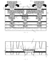
Figure 1 illustrates the FEOL and BEOL portions of an IC according to the invention, with a power gating transistor in the BEOL portion. -
Figure 2 shows an alternative lay-out of a power gating transistor in the BEOL portion. -
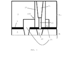
Figure 3 shows a vertically mounted power gating transistor mounted in the BEOL portion of an IC according to the invention. -
Figure 4 shows a process flow for producing a transistor that is applicable in an IC according to the invention. -
Figure 5 shows a detail of the transistor ofFigure 1 . -
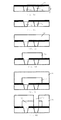
Figure 6 shows a process flow for producing a vertical transistor applicable in an IC according to the invention. - The invention is related to an integrated circuit device equipped with a plurality of power gating switches, wherein at least one of said power gating switches is a transistor located in the Back end of Line (BEOL) portion of the IC. In the context of the present description, the following definitions of the Front end of Line (FEOL) portion and BEOL portion of an IC are applicable. The FEOL portion comprises a processed semiconductor substrate, provided with a plurality of transistors and other devices, obtained by or obtainable by processing (e.g. litho/etch, STI, N+/P+ implants, gate deposition) a semiconductor wafer. The BEOL portion comprises a sequence of metallization layers for establishing electrical current paths between the FEOL portion and external terminals to which the IC is connected.
- According to preferred embodiments, said power gating switch located in the BEOL portion is a transistor having a gate electrode and source and drain electrodes, with said electrodes being formed by metal lines or metal-filled via interconnects present within the metallization layers of said BEOL portion. The term 'via' is known in the art (Vertical Interconnect Access), as a connection between metal lines in the BEOL. In an IC according to the invention, none of said gate, source and drain electrodes is formed by contact bumps at the top level of the device.
- The power gating transistor further comprises a channel region and a gate region that may be respectively in the form of a planar layer of a semiconductor material and a planar layer of a suitable gate dielectric material. The semiconductor layer is preferably a so-called thin film semiconductor layer deposited during BEOL processing, enabling to produce transistors with low leakage in the BEOL. The term thin film semiconductor refers to semiconductor material that can be deposited in the form of a layer of the material onto a supporting surface. A preferred choice for such thin film semiconductor material is Indium Gallium Zinc Oxide (hereafter referred to as IGZO). The term IGZO encompasses all realizable varieties of the compound InxGayZnzOw in terms of the values of the atomic numbers x,y,z and w, for example In2Ga2ZnO7. The use of IGZO or an equivalent material also allows to produce a power gating switch with a short turn-on and turn-off time due to the low threshold voltage of the transistor. This allows to apply power gating with low overhead in terms of power supply (low increase of required Vdd due to power gating). Also, the fact that the power gating switch is physically present in the current path between the access pins of the IC and the FEOL portion allows to reduce IR losses.
-
Figure 1 shows a possible implementation of apower gating transistor 100 implemented in a pair of two adjacent metallization layers in the BEOL portion of an IC device. The device's FEOL portion is schematically shown as arectangle 1, with the BEOL portion shown in a little more detail, as a sequence of metallization layers M1, M2, M3 and M4. Normally more than 4 metallization layers are present in an IC (currently up to 9 in 28nm technology), but only four are shown for the sake of simplifying the drawing.Cupper contact bumps 101/101' contact the upper metallization layer M4 throughAluminium contact pads 102/102'. Each metallization layer comprises an upper level comprising metal (preferably copper)lines 2 running in the plane of the layer, and a lower level comprising metal-filled viainterconnects 3 for connecting themetal lines 2 to the underlying layer. The metal lines and via interconnects are embedded in a layer of intermetal dielectric 4 (e.g. SiO2). Anotherdielectric layer 5, which may have one or more functions, for example the functions of a passivation layer, etch stop layer or diffusion barrier, may be present between the metallization layers, provided with openings where a connection is needed from one metallization layer to the next.Layers 5 may for example be layers of SiCN. Thegate electrode 10 of the transistor is formed by a metal line in metallization layer M3, whereas the source anddrain electrodes 11/12 are formed by two interconnect vias in metallization layer M4. A thinfilm semiconductor layer 13 forms the channel layer of the transistor. The thin film semiconductor layer is present on top of adielectric layer 14, deposited onto thedielectric layer 5 that is present between the metallization layers M3 and M4. The thin film semiconductor layer may be a layer of IGZO (as defined above). Thedielectric layer 14 may be a layer of Al2O3 or any other material or stack of materials qualifying as a high quality gate dielectric. Thedielectric layers power gating transistor 100. In the embodiment shown, the source anddrain electrodes 11/12 are described as 'interconnect vias', even though they do not 'connect' the M4 and M3 layer electrically. In defining the scope of the present invention and the appended claims, the term 'interconnect via' comprises any conductor obtainable by standard processing steps for producing actual interconnect vias in the BEOL, also when these interconnect vias are interrupted by a dielectric layer. -
Figure 2 shows another embodiment, wherein the source and drain electrodes of thepower gating transistor 100 are formed by a pair ofmetal lines 11/12 in a lower metallization layer Mn, while the gate electrode is formed by a metal-filled viainterconnect 10 in the upper metallization layer Mn+1. In this case, anopening 15 is present in thedielectric layer 5 between the two metallization layers, and a thinfilm semiconductor layer 13 forming a channel layer is deposited in said opening, on top of the source anddrain electrodes 11/12. A furtherdielectric layer 14 is present on top of the channel, preferably a high quality gate dielectric material such as Al2O3. Anotherdielectric layer 17 is present on thedielectric layer 14 and on the whole of the surface.Layer 17 may be an etch stop layer required during the etching of openings in theintermetal dielectric 4. The stack of thefirst dielectric 14 and theetch stop layer 17 together form the gate dielectric of thepower gating transistor 100. If thelayer 14 can itself act as an etch stop layer,layer 17 may be omitted or vice versa, if theetch stop layer 17 is a sufficiently good gate dielectric material,layer 14 could be omitted. Thechannel layer 13 is a thin film semiconductor layer, preferably a layer of IGZO. -
Figure 3 shows another embodiment of apower gating transistor 100 in the BEOL portion of an IC. The transistor is formed in two neighbouring metallization layers Mn and Mn+1, between afirst metal line 20 in layer Mn and ametal conductor 21 in layer Mn+1, themetal line 20 and theconductor 21 respectively forming the source and drain electrodes of the power gating transistor. The source and drain electrodes are thus physically located essentially one directly above the other. A via opening in Mn+1 and located above themetal line 20 comprises acentral channel portion 22, surrounded by agate dielectric material 23. The gate electrode is ametal conductor 24 that surrounds at least partially thegate dielectric material 23. Theconductor 21 in Mn+1 is equally located in the via opening. The channel material of thecentral channel portion 22 may be IGZO. Thegate dielectric material 23 may be Al2O3 or an equivalent high quality gate dielectric material. - The
power gating transistor 100 according to any of the above described embodiments is implemented within the BEOL portion of the IC, i.e. incorporated within the metallization layers of the IC. This approach allows the designer a high degree of flexibility in terms of defining the degree of fine grained or coarse grained power gating, without significant overhead in terms of semiconductor area. The location of the power gating switch in the vertical current path between the access pins of the IC and the FEOL portion also allows to reduce IR losses. With respect to the last point (IR losses), the embodiment ofFigure 2 is preferred, i.e. with thegate electrode 10 at the bottom of thetransistor 100, given that the signal for activating the power gating generally originates in the FEOL portion. - Apart from the physical location of the power gating switch, the incorporation of power gating transistors according to the invention in the electrical network of the IC is not different from power gating switches that are presently implemented in the FEOL. Blocks of standard cells in the IC's FEOL portion are defined on the chip, between Vdd and Vss rails through which the cells receive electrical power. The Vdd/Vss rails are connected to networks of Vdd and Vss lines in the BEOL, each network providing power to a block of standard cells. Power gating switches provide the capability of switching each network, and thereby each block, on or off individually.
- preferably a plurality of power gating switches are provided between a power source (e.g. a metal line or a metal ring in one upper metallization layer connected to an external power supply), and the power network of a block. In the example of
Figure 1 ,metal line 40 is connected to copper bump 101', which may be connected to the power source which can be an external supply voltage Vdd.Metal line 41 is then part of a Vdd power network configured to power a particular block on theFEOL portion 1 of the IC. Thetransistor 100 is configured to connectmetal line 41 and thereby the Vdd network configured to power a particular block to the power source voltage Vdd and thereby activate said block on the FEOL portion, or to disconnect said network configured to power a particular block and thus said FEOL block, from the power source voltage Vdd. - It should be noted that the power source is not restricted to an external power source. The IC can contain an internal power source, for instance a voltage regulator or switched mode power supply. These internal power sources are embedded in the FEOL of the IC. The internal power source may further be connected to the outside world. In the case of a voltage regulator, this may be done to stabilize the regulator output, for example by means of a capacitor, the source remaining however internal to the IC.
- It is preferred to implement power gating transistors according to the invention deep into the BEOL portion, i.e. in the metallization layers that are close to the FEOL portion, e.g. in metallization layer M1, M2, M3, in order to enable fine grained power gating of a large number of blocks of standard cells on the IC. In this way, the present invention allows fine grained power gating without excessive area consumption on the chip and with lower IR losses compared to ICs where the power gating switches are in the FEOL portion. According to an embodiment, a power gating transistor is located on the power delivery strips of the standard cell rows of the FEOL portion.
- A process sequence for producing a transistor between two BEOL metallization layers according to the embodiment of
Figure 2 is illustrated inFigure 4 .Figure 4a shows the upper level of a first metallization layer Mn, comprising a number ofmetal lines 48, the intermetal dielectric 49 (preferably SiO2) and apassivation layer 50, e.g. a layer of SiCN. Anopening 51 is etched in thepassivation layer 50 by known litho/etch steps (Figure 4b ). The opening exposes at least a portion of twometal lines 52/53 in the Mn layer. After that, athin film layer 54 of IGZO and alayer 55 of a suitable gate dielectric material, e.g. Al2O3 are sequentially deposited by a suitable deposition technique (Figure 4c ). For example, a layer of between 10nm and 50nm of IGZO is deposited by PVD (Physical Vapour Deposition) and a layer of between 10nm and 50nm of Al2O3 is deposited on and in contact with the IGZO by ALD (Atomic Layer Deposition). Suitable conditions for the PVD and ALD processes are known to the skilled reader and not described here in detail. A patterning of the IGZO/Al2O3 stack is then performed, to obtain thestack 54/55 only on the required location (Figure 4d ). Anadditional dielectric layer 56, for example a SiCN layer is deposited over the complete surface, covering thestack 56. This layer will act as etch stop layer during subsequent etching steps. Then the intermetaldielectric layer 57 of the next metallization layer Mn+1 is deposited, followed by deposition of a Bottom Anti-Reflective Coating (BARC)layer 58, in turn followed by the deposition and patterning of a resist layer 59 (Figure 4e ). Through the patterned resist layer, theIMD layer 57 is etched a first time for forming trenches destined to be filled by metal lines in the upper level of Mn+1 (Figure 4f ), after which asecond BARC 60 and resist 61 are deposited and the second resist is patterned, after which a second etching step is done, to form openings destined to be filled by interconnect vias in the lower level of Mn+1 (Figure 4g and 4h ). Etching of the vias stops on theetch stop layer 56. If thelayer 55 can act as an etch stop layer,layer 56 may be omitted from the process. Metal deposition, preferably deposition of a seed layer and electrodeposition of copper, into the patterned trenches and vias is performed for forming all metal lines and interconnects, including thetransistor gate electrode 62 on top of the IGZO/Al2O3/SiCN stack (Figure 4i ). The described method step sequence does not exclude the presence of other method steps in between the steps of the sequence. Method steps that are routinely applied during BEOL processing have not been included in the above description for the sake of conciseness. For example, diffusion barrier layers will need to be deposited prior to deposition of metal lines and interconnect vias. In particular, in between the Cu metallization and the IGZO, a conductive layer is required that works as a diffusion barrier to the Cu. This can be e.g. a layer of Co, TaN, TiN. - The embodiment of
Figure 1 can be processed by a similar process sequence, wherein however no patterning is required of thedielectric layer 5. The stack oflayers passivation layer 5, but in the inverse order compared toFigure 2 : first agate dielectric layer 55 is deposited on thedielectric layer 5, followed by deposition of a thin film semiconductor layer 54 (preferably IGZO), after which the stack of these two layers is patterned to form astack 55/54 only on top of ametal line 10 in a metallization layer Mn. Then anetch stop layer 56 is deposited (if required) and on top of said etch stop layer, a suitable set of litho/etch steps is performed, involving correctly defined resist masks, for producing metal-filledinterconnect vias metal lines 41/40 connected to said vias. When theetch stop layer 56 is applied, this results in a power gating transistor as shown inFigure 5 . As seen in this figure, theetch stop layer 56 itself is locally removed at the location of the source and drain 11/12. As known by the skilled person, this can be done by an additional litho/etch step, prior to the deposition of the metal-filled interconnect vias and metal lines. -
Figure 6 illustrates a possible process flow for producing a power gating transistor as shown inFigure 3 . On a given metallization layer Mn comprisingmetal lines Figure 6a ), the SiCN layer is opened by a suitable litho/etch step above one of the metal lines 70 (Figure 6b ). Then a metal layer 72 is deposited over the complete surface (Figure 6c ). This may for example be a Ta layer. The Ta layer is itself patterned by litho/etch, so that aconductor 73 remains only on top of themetal lines 70/71 (Figure 6d ). Alayer 74 of intermetal dielectric, e.g. SiO2 (Figure 6e ) is then deposited, followed by litho/etch to open up said IMD layer above the second metal line 71 (Figure 6f ) and form a viaopening 75 through the IMD layer and through theconductor 73. A dielectric material suitable to serve as a gate dielectric, for example Al2O3 is deposited in the via opening, for example by ALD (atomic layer deposition), to form alayer 76 that lines the side wall and bottom of the opening and the upper surface of the IMD (Figure 6g ). - The ALD deposited
layer 76 is then removed from the upper surface of the IMD and from the bottom of the opening by a dry etching step, stopping on theSiCN layer 5, creating a narrowed opening with slantedsidewalls 77 formed of the gate dielectric material (Figure 6h ). TheSiCN layer 5 is then itself removed from the bottom of the opening (Figure 6i ). Then asemiconductor material 78, for example a metal oxide with semiconductor properties, such as IGZO is deposited in the opening (Figure 6j ). This can be done by growing an IGZO nanowire or by MOCVD (Metal Organic Chemical Vapour Deposition) or ALD of IGZO in the opening. The IGZO material is then etched back inside the opening, to about the upper level of the Ta conductor (Figure 6k ), after which metal is deposited in the manner known in BEOL processing (e.g. Cu deposition including anti-diffusion layer, seed layer, copper plating) to form aconductor 79 at the top (Figure 6l ) and thereby obtain the vertical transistor that is suitable to serve as a power gating transistor in an IC according to the invention. - The thin film semiconductor material that is applicable in an IC according to the invention must be suitable for producing a low leakage transistor. The thin film semiconductor layer is furthermore a layer that can be deposited, for example by PVD, CVD, ALD, solution deposition, on an amorphous substrate, i.e. it does not require a crystalline template. The thin film semiconductor must also be compatible with the thermal budget of BEOL processing, i.e. the material must not degrade at the temperatures used in the BEOL part of the IC's production process (typically 350-380°C). IGZO is a preferred option for the thin film semiconductor, but other materials may be possible, such as amorphous silicon, monocrystalline or polycrystalline silicon, graphene, Carbon nano tubes or metal oxides other than IGZO, e.g. ZnO, HfInZnO, SnO, CuO.
- While the invention has been illustrated and described in detail in the drawings and foregoing description, such illustration and description are to be considered illustrative or exemplary and not restrictive. Other variations to the disclosed embodiments can be understood and effected by those skilled in the art in practicing the claimed invention, from a study of the drawings, the disclosure and the appended claims. In the claims, the word "comprising" does not exclude other elements or steps, and the indefinite article "a" or "an" does not exclude a plurality. The mere fact that certain measures are recited in mutually different dependent claims does not indicate that a combination of these measures cannot be used to advantage. Any reference signs in the claims should not be construed as limiting the scope.
- The foregoing description details certain embodiments of the invention. It will be appreciated, however, that no matter how detailed the foregoing appears in text, the invention may be practiced in many ways, and is therefore not limited to the embodiments disclosed. It should be noted that the use of particular terminology when describing certain features or aspects of the invention should not be taken to imply that the terminology is being re-defined herein to be restricted to include any specific characteristics of the features or aspects of the invention with which that terminology is associated.
- Unless specifically specified, the description of a layer being present, deposited or produced 'on' another layer or substrate, includes the options of
- said layer being present, produced or deposited directly on, i.e. in physical contact with, said other layer or substrate, and
Claims (10)
- An integrated circuit (IC) device comprising a front-end-of-line portion (1) and a back-end-of-line (BEOL) portion, the BEOL portion comprising a plurality of metallization layers (Mn), said layers comprising metal lines (2) and metal-filled interconnect vias (3), the IC further comprising a plurality of power gating transistors wherein at least one of said power gating transistors (100) is located in said BEOL portion.
- Integrated circuit device according to claim 1, wherein said at least one power gating transistor (100) in the BEOL portion comprises a gate electrode (10,24), a source electrode and a drain electrode (11,12,20,21), a channel region (13,22) and a gate dielectric region (5,14,17,23), wherein said gate, source and drain electrodes are formed by metal lines or metal-filled interconnect vias of said metallization layers.
- Integrated circuit device according to claim 2, wherein said channel region (13,) is a planar semiconductor layer, and wherein said gate dielectric region (5,14,17) is a planar layer of dielectric material and wherein said layers form a stack of layers between the gate electrode (10) on the one hand and the source and drain electrodes (11,12) on the other hand.
- Integrated circuit device according to claim 3, wherein said gate electrode is formed by a metal line (10) in a first metallization layer (Mn), and the source and drain electrodes are formed by metal-filled interconnect vias (11,12) in a second metallization layer (Mn+1) directly on top of the first metallization layer (Mn).
- Integrated circuit device according to claim 3, wherein said source and drain electrodes (10,11) are formed by a pair of metal lines in a first metallization layer (Mn) and the gate electrode (10) is formed by a metal-filled via interconnect (10) in a second metallization layer (Mn+1) directly on top of the first metallization layer (Mn).
- Integrated circuit device according to claim 1, wherein said at least one power gating transistor (100) in the BEOL portion comprises a gate electrode(24), a source electrode and a drain electrode, a channel region (22) and a gate dielectric region (23), wherein said source and drain electrodes (20,21) are formed by a pair of conductors, the first conductor (20) being located in a first metallization layer (Mn), the second conductor (21) in a second metallization layer (Mn+1) which is directly on top of the first metallization layer (Mn), the source and drain electrodes being physically located essentially one directly above the other, with the channel region (22) being located in between the source and drain electrodes (20,21) and the channel region (22) being in electrical contact with the source and drain electrodes (20,21), the channel region (22) and gate dielectric region (23) being located in a via opening located above the first conductor (20), the gate dielectric region surrounding the channel region, and wherein the gate electrode (24) is a conductor in contact with the gate dielectric (23) and formed at least partially surrounding said via opening.
- Integrated circuit according to claim 6, wherein the second conductor (21) is also located in said via opening.
- Integrated circuit according to claim 6 or 7, wherein the first conductor (20) is a metal line in the first metallization layer (Mn).
- Integrated circuit device according to any one of claims 1 to 8, wherein said channel region is formed of Indium Gallium Zinc Oxide (IGZO).
- Integrated circuit device according to any one of the preceding claims, wherein said power gating transistor is located in the three first metallization layers (M1,M2,M3) of the device.
Priority Applications (1)
| Application Number | Priority Date | Filing Date | Title |
|---|---|---|---|
| EP14191497.8A EP2884542A3 (en) | 2013-12-10 | 2014-11-03 | Integrated circuit device with power gating switch in back end of line |
Applications Claiming Priority (2)
| Application Number | Priority Date | Filing Date | Title |
|---|---|---|---|
| EP13196413 | 2013-12-10 | ||
| EP14191497.8A EP2884542A3 (en) | 2013-12-10 | 2014-11-03 | Integrated circuit device with power gating switch in back end of line |
Publications (2)
| Publication Number | Publication Date |
|---|---|
| EP2884542A2 true EP2884542A2 (en) | 2015-06-17 |
| EP2884542A3 EP2884542A3 (en) | 2015-09-02 |
Family
ID=49765831
Family Applications (1)
| Application Number | Title | Priority Date | Filing Date |
|---|---|---|---|
| EP14191497.8A Withdrawn EP2884542A3 (en) | 2013-12-10 | 2014-11-03 | Integrated circuit device with power gating switch in back end of line |
Country Status (3)
| Country | Link |
|---|---|
| US (1) | US20150162448A1 (en) |
| EP (1) | EP2884542A3 (en) |
| KR (1) | KR20150067730A (en) |
Cited By (3)
| Publication number | Priority date | Publication date | Assignee | Title |
|---|---|---|---|---|
| EP3273325A1 (en) | 2016-07-20 | 2018-01-24 | IMEC vzw | Power control in integrated circuits |
| US12027416B2 (en) | 2021-09-16 | 2024-07-02 | International Business Machines Corporation | BEOL etch stop layer without capacitance penalty |
| US12382719B2 (en) | 2022-09-30 | 2025-08-05 | International Business Machines Corporation | Power gating dummy power transistors for back side power delivery networks |
Families Citing this family (31)
| Publication number | Priority date | Publication date | Assignee | Title |
|---|---|---|---|---|
| US8969154B2 (en) * | 2011-08-23 | 2015-03-03 | Micron Technology, Inc. | Methods for fabricating semiconductor device structures and arrays of vertical transistor devices |
| WO2016160775A1 (en) * | 2015-03-30 | 2016-10-06 | Murata Manufacturing Co., Ltd. | High-frequency transformer design for dc/dc resonant converters |
| US9466452B1 (en) | 2015-03-31 | 2016-10-11 | Stmicroelectronics, Inc. | Integrated cantilever switch |
| FR3034567B1 (en) | 2015-03-31 | 2017-04-28 | St Microelectronics Rousset | METALLIC DEVICE WITH IMPROVED MOBILE PIECE (S) LOADED IN A CAVITY OF THE INTERCONNECTION PART ("BEOL") OF AN INTEGRATED CIRCUIT |
| US10659046B2 (en) * | 2015-09-25 | 2020-05-19 | Intel Corporation | Local cell-level power gating switch |
| US9520876B1 (en) | 2016-02-17 | 2016-12-13 | International Business Machines Corporation | Power gating and clock gating in wiring levels |
| US9754923B1 (en) | 2016-05-09 | 2017-09-05 | Qualcomm Incorporated | Power gate placement techniques in three-dimensional (3D) integrated circuits (ICs) (3DICs) |
| WO2018004537A1 (en) * | 2016-06-28 | 2018-01-04 | Intel Corporation | Integration of single crystalline transistors in back end of line (beol) |
| US10644140B2 (en) | 2016-06-30 | 2020-05-05 | Intel Corporation | Integrated circuit die having back-end-of-line transistors |
| WO2018004652A1 (en) * | 2016-07-01 | 2018-01-04 | Intel Corporation | Front-end tunnel junction device plus back-end transistor device |
| CN106756877B (en) * | 2016-12-13 | 2019-02-19 | 武汉华星光电技术有限公司 | C-axis crystalline IGZO thin film and preparation method thereof |
| WO2019132984A1 (en) * | 2017-12-29 | 2019-07-04 | Intel Corp | Metal-assisted single crystal transistors |
| US20190385657A1 (en) * | 2018-06-19 | 2019-12-19 | Intel Corporation | High density negative differential resistance based memory |
| US11017146B2 (en) | 2018-07-16 | 2021-05-25 | Taiwan Semiconductor Manufacturing Company, Ltd. | Integrated circuit and method of forming the same |
| CN109326578B (en) * | 2018-09-07 | 2021-02-26 | 上海兆芯集成电路有限公司 | Power supply network and wiring method thereof |
| US11264506B2 (en) * | 2018-10-31 | 2022-03-01 | Taiwan Semiconductor Manufacturing Co., Ltd. | Semiconductor device and manufacturing method thereof |
| US10971609B2 (en) * | 2019-08-23 | 2021-04-06 | Taiwan Semiconductor Manufacturing Co., Ltd. | Back end of line nanowire power switch transistors |
| CN114514604B (en) | 2019-10-11 | 2024-10-29 | 株式会社索思未来 | Semiconductor devices |
| WO2021070367A1 (en) | 2019-10-11 | 2021-04-15 | 株式会社ソシオネクスト | Semiconductor device |
| WO2021079511A1 (en) | 2019-10-25 | 2021-04-29 | 株式会社ソシオネクスト | Semiconductor device |
| CN114762113B (en) | 2019-12-05 | 2024-11-01 | 株式会社索思未来 | Semiconductor devices |
| KR102262756B1 (en) * | 2020-02-13 | 2021-06-08 | 성균관대학교산학협력단 | 3D semiconductor integrated circuit |
| US11456242B2 (en) * | 2020-07-21 | 2022-09-27 | Nanya Technology Corporation | Semiconductor device with stress-relieving structures and method for fabricating the same |
| US11668735B2 (en) | 2020-07-21 | 2023-06-06 | Qualcomm Incorporated | Granular sensing on an integrated circuit |
| US11270991B1 (en) * | 2020-09-02 | 2022-03-08 | Qualcomm Incorporated | Integrated circuits (ICs) employing front side (FS) back end-of-line (BEOL) (FS-BEOL) input/output (I/O) routing and back side (BS) BEOL (BS-BEOL) power routing for current flow organization, and related methods |
| US12598979B2 (en) | 2022-03-21 | 2026-04-07 | Apple Inc. | Dual contact and power rail for high performance standard cells |
| US12543555B2 (en) | 2022-03-21 | 2026-02-03 | Apple Inc. | Backside routing implementation in SRAM arrays |
| CN115172365A (en) * | 2022-05-11 | 2022-10-11 | 中国科学院微电子研究所 | Three-dimensional integrated circuit and manufacturing method thereof |
| US12511463B2 (en) | 2022-08-31 | 2025-12-30 | Apple Inc. | Backside contacts for signal routing |
| US20250174597A1 (en) * | 2023-11-29 | 2025-05-29 | Taiwan Semiconductor Manufacturing Co., Ltd. | Embedded integrated voltage regulator |
| KR20250105801A (en) * | 2023-12-29 | 2025-07-09 | 삼성전자주식회사 | Semiconductor device with power gating element |
Family Cites Families (38)
| Publication number | Priority date | Publication date | Assignee | Title |
|---|---|---|---|---|
| US4489478A (en) * | 1981-09-29 | 1984-12-25 | Fujitsu Limited | Process for producing a three-dimensional semiconductor device |
| JPH0612799B2 (en) * | 1986-03-03 | 1994-02-16 | 三菱電機株式会社 | Stacked semiconductor device and manufacturing method thereof |
| AU588700B2 (en) * | 1986-06-30 | 1989-09-21 | Canon Kabushiki Kaisha | Semiconductor device and method for producing the same |
| JP2516604B2 (en) * | 1986-10-17 | 1996-07-24 | キヤノン株式会社 | Method for manufacturing complementary MOS integrated circuit device |
| US5155058A (en) * | 1986-11-07 | 1992-10-13 | Canon Kabushiki Kaisha | Method of making semiconductor memory device |
| DE4400985C1 (en) * | 1994-01-14 | 1995-05-11 | Siemens Ag | Method for producing a three-dimensional circuit arrangement |
| US5670812A (en) * | 1995-09-29 | 1997-09-23 | International Business Machines Corporation | Field effect transistor having contact layer of transistor gate electrode material |
| US5675185A (en) * | 1995-09-29 | 1997-10-07 | International Business Machines Corporation | Semiconductor structure incorporating thin film transistors with undoped cap oxide layers |
| JPH09260669A (en) * | 1996-03-19 | 1997-10-03 | Nec Corp | Semiconductor device and manufacturing method thereof |
| US5770483A (en) * | 1996-10-08 | 1998-06-23 | Advanced Micro Devices, Inc. | Multi-level transistor fabrication method with high performance drain-to-gate connection |
| US7052941B2 (en) * | 2003-06-24 | 2006-05-30 | Sang-Yun Lee | Method for making a three-dimensional integrated circuit structure |
| US5872029A (en) * | 1996-11-07 | 1999-02-16 | Advanced Micro Devices, Inc. | Method for forming an ultra high density inverter using a stacked transistor arrangement |
| US5818069A (en) * | 1997-06-20 | 1998-10-06 | Advanced Micro Devices, Inc. | Ultra high density series-connected transistors formed on separate elevational levels |
| US6030860A (en) * | 1997-12-19 | 2000-02-29 | Advanced Micro Devices, Inc. | Elevated substrate formation and local interconnect integrated fabrication |
| US6016000A (en) * | 1998-04-22 | 2000-01-18 | Cvc, Inc. | Ultra high-speed chip semiconductor integrated circuit interconnect structure and fabrication method using free-space dielectrics |
| US6215130B1 (en) * | 1998-08-20 | 2001-04-10 | Lucent Technologies Inc. | Thin film transistors |
| US6635552B1 (en) * | 2000-06-12 | 2003-10-21 | Micron Technology, Inc. | Methods of forming semiconductor constructions |
| JP4472340B2 (en) * | 2001-11-05 | 2010-06-02 | 株式会社ザイキューブ | Semiconductor device using low dielectric constant material film and manufacturing method thereof |
| JP2003338559A (en) * | 2002-03-13 | 2003-11-28 | Sony Corp | Semiconductor device and semiconductor manufacturing method |
| KR100508545B1 (en) * | 2002-12-14 | 2005-08-17 | 한국전자통신연구원 | Thin film transistor with vertical structure |
| US20070194450A1 (en) * | 2006-02-21 | 2007-08-23 | Tyberg Christy S | BEOL compatible FET structure |
| JP2009076879A (en) * | 2007-08-24 | 2009-04-09 | Semiconductor Energy Lab Co Ltd | Semiconductor device |
| US8044464B2 (en) * | 2007-09-21 | 2011-10-25 | Semiconductor Energy Laboratory Co., Ltd. | Semiconductor device |
| JP5781720B2 (en) * | 2008-12-15 | 2015-09-24 | ルネサスエレクトロニクス株式会社 | Semiconductor device and manufacturing method of semiconductor device |
| US8507359B2 (en) * | 2009-12-02 | 2013-08-13 | Sharp Kabushiki Kaisha | Semiconductor device, process for producing same, and display device |
| KR101770976B1 (en) * | 2009-12-11 | 2017-08-24 | 가부시키가이샤 한도오따이 에네루기 켄큐쇼 | Semiconductor device |
| WO2012002186A1 (en) * | 2010-07-02 | 2012-01-05 | Semiconductor Energy Laboratory Co., Ltd. | Semiconductor device |
| US8624323B2 (en) * | 2011-05-31 | 2014-01-07 | International Business Machines Corporation | BEOL structures incorporating active devices and mechanical strength |
| US8891285B2 (en) * | 2011-06-10 | 2014-11-18 | Semiconductor Energy Laboratory Co., Ltd. | Semiconductor memory device |
| JP5876249B2 (en) * | 2011-08-10 | 2016-03-02 | ルネサスエレクトロニクス株式会社 | Semiconductor device and manufacturing method of semiconductor device |
| US9177872B2 (en) * | 2011-09-16 | 2015-11-03 | Micron Technology, Inc. | Memory cells, semiconductor devices, systems including such cells, and methods of fabrication |
| JP5981711B2 (en) * | 2011-12-16 | 2016-08-31 | ルネサスエレクトロニクス株式会社 | Semiconductor device and manufacturing method of semiconductor device |
| JP6013084B2 (en) * | 2012-08-24 | 2016-10-25 | ルネサスエレクトロニクス株式会社 | Semiconductor device and manufacturing method of semiconductor device |
| JP5960000B2 (en) * | 2012-09-05 | 2016-08-02 | ルネサスエレクトロニクス株式会社 | Semiconductor device and manufacturing method of semiconductor device |
| JP2015035506A (en) * | 2013-08-09 | 2015-02-19 | 株式会社東芝 | Semiconductor device |
| JP2015038925A (en) * | 2013-08-19 | 2015-02-26 | 株式会社東芝 | Semiconductor device |
| EP2884666B1 (en) * | 2013-12-10 | 2019-01-02 | IMEC vzw | FPGA device with programmable interconnect in back end of line portion of the device. |
| JP2015162633A (en) * | 2014-02-28 | 2015-09-07 | 株式会社東芝 | Semiconductor device |
-
2014
- 2014-11-03 EP EP14191497.8A patent/EP2884542A3/en not_active Withdrawn
- 2014-12-05 KR KR1020140173504A patent/KR20150067730A/en not_active Ceased
- 2014-12-09 US US14/565,159 patent/US20150162448A1/en not_active Abandoned
Non-Patent Citations (1)
| Title |
|---|
| None |
Cited By (4)
| Publication number | Priority date | Publication date | Assignee | Title |
|---|---|---|---|---|
| EP3273325A1 (en) | 2016-07-20 | 2018-01-24 | IMEC vzw | Power control in integrated circuits |
| US10331201B2 (en) | 2016-07-20 | 2019-06-25 | Imec Vzw | Power control in integrated circuits |
| US12027416B2 (en) | 2021-09-16 | 2024-07-02 | International Business Machines Corporation | BEOL etch stop layer without capacitance penalty |
| US12382719B2 (en) | 2022-09-30 | 2025-08-05 | International Business Machines Corporation | Power gating dummy power transistors for back side power delivery networks |
Also Published As
| Publication number | Publication date |
|---|---|
| EP2884542A3 (en) | 2015-09-02 |
| US20150162448A1 (en) | 2015-06-11 |
| KR20150067730A (en) | 2015-06-18 |
Similar Documents
| Publication | Publication Date | Title |
|---|---|---|
| US20150162448A1 (en) | Integrated circuit device with power gating switch in back end of line | |
| US11031327B2 (en) | Through vias and methods of formation thereof | |
| US6355950B1 (en) | Substrate interconnect for power distribution on integrated circuits | |
| EP2884666B1 (en) | FPGA device with programmable interconnect in back end of line portion of the device. | |
| US12074162B2 (en) | Structure and formation method of semiconductor device with capacitors | |
| US12119262B2 (en) | Semiconductor device structure with resistive element | |
| US20150270176A1 (en) | Methods of forming reduced resistance local interconnect structures and the resulting devices | |
| US20210249251A1 (en) | Semiconductor device structure with resistive elements | |
| US12057489B2 (en) | Ferroelectric field effect transistor | |
| US11901289B2 (en) | Semiconductor device structure with resistive element | |
| US10832961B1 (en) | Sacrificial gate spacer regions for gate contacts formed over the active region of a transistor | |
| US20240072050A1 (en) | Field-effect transistors with isolation pillars | |
| US20230335578A1 (en) | Device structure and methods of forming the same | |
| US20210082913A1 (en) | Single diffusion break local interconnect | |
| US9406883B1 (en) | Structure and formation method of memory device | |
| CN222721870U (en) | Inverter circuit and semiconductor circuit | |
| US20240105608A1 (en) | Local frontside power rail with global backside power delivery | |
| US12419113B2 (en) | Back-end-of-line semiconductor device structure providing a not-gate logic function and methods of forming the same | |
| CN106024697A (en) | Trench power device and manufacturing method | |
| US20240355771A1 (en) | Chip package structure with substrates and method for forming the same | |
| TW202537422A (en) | Transistor structure, semiconductor device, and methods of formation |
Legal Events
| Date | Code | Title | Description |
|---|---|---|---|
| PUAI | Public reference made under article 153(3) epc to a published international application that has entered the european phase |
Free format text: ORIGINAL CODE: 0009012 |
|
| 17P | Request for examination filed |
Effective date: 20141103 |
|
| AK | Designated contracting states |
Kind code of ref document: A2 Designated state(s): AL AT BE BG CH CY CZ DE DK EE ES FI FR GB GR HR HU IE IS IT LI LT LU LV MC MK MT NL NO PL PT RO RS SE SI SK SM TR |
|
| AX | Request for extension of the european patent |
Extension state: BA ME |
|
| PUAL | Search report despatched |
Free format text: ORIGINAL CODE: 0009013 |
|
| AK | Designated contracting states |
Kind code of ref document: A3 Designated state(s): AL AT BE BG CH CY CZ DE DK EE ES FI FR GB GR HR HU IE IS IT LI LT LU LV MC MK MT NL NO PL PT RO RS SE SI SK SM TR |
|
| AX | Request for extension of the european patent |
Extension state: BA ME |
|
| RIC1 | Information provided on ipc code assigned before grant |
Ipc: H01L 29/786 20060101AFI20150727BHEP Ipc: H03K 19/00 20060101ALI20150727BHEP Ipc: H01L 23/532 20060101ALI20150727BHEP Ipc: H01L 23/525 20060101ALI20150727BHEP Ipc: H01L 23/00 20060101ALI20150727BHEP Ipc: H01L 23/528 20060101ALI20150727BHEP Ipc: H01L 27/12 20060101ALI20150727BHEP Ipc: H01L 21/768 20060101ALI20150727BHEP Ipc: H03K 17/687 20060101ALI20150727BHEP Ipc: H01L 29/66 20060101ALI20150727BHEP |
|
| STAA | Information on the status of an ep patent application or granted ep patent |
Free format text: STATUS: THE APPLICATION IS DEEMED TO BE WITHDRAWN |
|
| 18D | Application deemed to be withdrawn |
Effective date: 20160303 |