EP2884260A1 - Plasmonic wavelength selective switch - Google Patents
Plasmonic wavelength selective switch Download PDFInfo
- Publication number
- EP2884260A1 EP2884260A1 EP13197308.3A EP13197308A EP2884260A1 EP 2884260 A1 EP2884260 A1 EP 2884260A1 EP 13197308 A EP13197308 A EP 13197308A EP 2884260 A1 EP2884260 A1 EP 2884260A1
- Authority
- EP
- European Patent Office
- Prior art keywords
- radiation
- plasmonic structure
- plasmonic
- wavelength
- incident
- Prior art date
- Legal status (The legal status is an assumption and is not a legal conclusion. Google has not performed a legal analysis and makes no representation as to the accuracy of the status listed.)
- Granted
Links
- 230000005855 radiation Effects 0.000 claims abstract description 164
- 239000004020 conductor Substances 0.000 claims abstract description 34
- 239000000758 substrate Substances 0.000 claims abstract description 26
- 238000001514 detection method Methods 0.000 claims description 35
- 238000000034 method Methods 0.000 claims description 30
- 230000005284 excitation Effects 0.000 claims description 10
- 239000011521 glass Substances 0.000 claims description 10
- 238000001914 filtration Methods 0.000 claims description 4
- 238000012545 processing Methods 0.000 claims description 3
- 238000001228 spectrum Methods 0.000 description 14
- 230000008033 biological extinction Effects 0.000 description 8
- 230000003595 spectral effect Effects 0.000 description 8
- 230000001419 dependent effect Effects 0.000 description 6
- 239000000975 dye Substances 0.000 description 6
- PCHJSUWPFVWCPO-UHFFFAOYSA-N gold Chemical compound [Au] PCHJSUWPFVWCPO-UHFFFAOYSA-N 0.000 description 6
- 239000000463 material Substances 0.000 description 6
- 230000003287 optical effect Effects 0.000 description 6
- 239000010931 gold Substances 0.000 description 5
- 229910052737 gold Inorganic materials 0.000 description 5
- 229910000510 noble metal Inorganic materials 0.000 description 4
- 238000010521 absorption reaction Methods 0.000 description 3
- 238000000862 absorption spectrum Methods 0.000 description 3
- 229910052782 aluminium Inorganic materials 0.000 description 3
- XAGFODPZIPBFFR-UHFFFAOYSA-N aluminium Chemical compound [Al] XAGFODPZIPBFFR-UHFFFAOYSA-N 0.000 description 3
- 230000003247 decreasing effect Effects 0.000 description 3
- 230000001066 destructive effect Effects 0.000 description 3
- 230000000694 effects Effects 0.000 description 3
- 230000003993 interaction Effects 0.000 description 3
- 238000002955 isolation Methods 0.000 description 3
- ORQBXQOJMQIAOY-UHFFFAOYSA-N nobelium Chemical compound [No] ORQBXQOJMQIAOY-UHFFFAOYSA-N 0.000 description 3
- 238000002198 surface plasmon resonance spectroscopy Methods 0.000 description 3
- VYPSYNLAJGMNEJ-UHFFFAOYSA-N Silicium dioxide Chemical compound O=[Si]=O VYPSYNLAJGMNEJ-UHFFFAOYSA-N 0.000 description 2
- 239000004411 aluminium Substances 0.000 description 2
- 230000007423 decrease Effects 0.000 description 2
- 239000002105 nanoparticle Substances 0.000 description 2
- 238000001429 visible spectrum Methods 0.000 description 2
- 229910052581 Si3N4 Inorganic materials 0.000 description 1
- XUIMIQQOPSSXEZ-UHFFFAOYSA-N Silicon Chemical compound [Si] XUIMIQQOPSSXEZ-UHFFFAOYSA-N 0.000 description 1
- BQCADISMDOOEFD-UHFFFAOYSA-N Silver Chemical compound [Ag] BQCADISMDOOEFD-UHFFFAOYSA-N 0.000 description 1
- 230000005540 biological transmission Effects 0.000 description 1
- 238000005253 cladding Methods 0.000 description 1
- 239000011248 coating agent Substances 0.000 description 1
- 238000000576 coating method Methods 0.000 description 1
- 238000013461 design Methods 0.000 description 1
- 230000005684 electric field Effects 0.000 description 1
- 230000005670 electromagnetic radiation Effects 0.000 description 1
- 239000012530 fluid Substances 0.000 description 1
- 239000012212 insulator Substances 0.000 description 1
- 230000010354 integration Effects 0.000 description 1
- 238000004519 manufacturing process Methods 0.000 description 1
- 238000005259 measurement Methods 0.000 description 1
- 239000007769 metal material Substances 0.000 description 1
- 239000002086 nanomaterial Substances 0.000 description 1
- 230000009467 reduction Effects 0.000 description 1
- 238000000926 separation method Methods 0.000 description 1
- 229910052710 silicon Inorganic materials 0.000 description 1
- 239000010703 silicon Substances 0.000 description 1
- 235000012239 silicon dioxide Nutrition 0.000 description 1
- 239000000377 silicon dioxide Substances 0.000 description 1
- HQVNEWCFYHHQES-UHFFFAOYSA-N silicon nitride Chemical compound N12[Si]34N5[Si]62N3[Si]51N64 HQVNEWCFYHHQES-UHFFFAOYSA-N 0.000 description 1
- 239000004332 silver Substances 0.000 description 1
- 229910052709 silver Inorganic materials 0.000 description 1
- 238000004088 simulation Methods 0.000 description 1
- 238000010183 spectrum analysis Methods 0.000 description 1
Images






Classifications
-
- B—PERFORMING OPERATIONS; TRANSPORTING
- B82—NANOTECHNOLOGY
- B82Y—SPECIFIC USES OR APPLICATIONS OF NANOSTRUCTURES; MEASUREMENT OR ANALYSIS OF NANOSTRUCTURES; MANUFACTURE OR TREATMENT OF NANOSTRUCTURES
- B82Y10/00—Nanotechnology for information processing, storage or transmission, e.g. quantum computing or single electron logic
-
- G—PHYSICS
- G01—MEASURING; TESTING
- G01N—INVESTIGATING OR ANALYSING MATERIALS BY DETERMINING THEIR CHEMICAL OR PHYSICAL PROPERTIES
- G01N21/00—Investigating or analysing materials by the use of optical means, i.e. using sub-millimetre waves, infrared, visible or ultraviolet light
- G01N21/62—Systems in which the material investigated is excited whereby it emits light or causes a change in wavelength of the incident light
- G01N21/63—Systems in which the material investigated is excited whereby it emits light or causes a change in wavelength of the incident light optically excited
- G01N21/64—Fluorescence; Phosphorescence
- G01N21/6428—Measuring fluorescence of fluorescent products of reactions or of fluorochrome labelled reactive substances, e.g. measuring quenching effects, using measuring "optrodes"
-
- G—PHYSICS
- G01—MEASURING; TESTING
- G01N—INVESTIGATING OR ANALYSING MATERIALS BY DETERMINING THEIR CHEMICAL OR PHYSICAL PROPERTIES
- G01N21/00—Investigating or analysing materials by the use of optical means, i.e. using sub-millimetre waves, infrared, visible or ultraviolet light
- G01N21/62—Systems in which the material investigated is excited whereby it emits light or causes a change in wavelength of the incident light
- G01N21/63—Systems in which the material investigated is excited whereby it emits light or causes a change in wavelength of the incident light optically excited
- G01N21/64—Fluorescence; Phosphorescence
- G01N21/645—Specially adapted constructive features of fluorimeters
- G01N21/648—Specially adapted constructive features of fluorimeters using evanescent coupling or surface plasmon coupling for the excitation of fluorescence
-
- G—PHYSICS
- G02—OPTICS
- G02B—OPTICAL ELEMENTS, SYSTEMS OR APPARATUS
- G02B5/00—Optical elements other than lenses
- G02B5/008—Surface plasmon devices
-
- G—PHYSICS
- G02—OPTICS
- G02B—OPTICAL ELEMENTS, SYSTEMS OR APPARATUS
- G02B6/00—Light guides; Structural details of arrangements comprising light guides and other optical elements, e.g. couplings
- G02B6/10—Light guides; Structural details of arrangements comprising light guides and other optical elements, e.g. couplings of the optical waveguide type
- G02B6/12—Light guides; Structural details of arrangements comprising light guides and other optical elements, e.g. couplings of the optical waveguide type of the integrated circuit kind
- G02B6/12007—Light guides; Structural details of arrangements comprising light guides and other optical elements, e.g. couplings of the optical waveguide type of the integrated circuit kind forming wavelength selective elements, e.g. multiplexer, demultiplexer
-
- G—PHYSICS
- G02—OPTICS
- G02B—OPTICAL ELEMENTS, SYSTEMS OR APPARATUS
- G02B6/00—Light guides; Structural details of arrangements comprising light guides and other optical elements, e.g. couplings
- G02B6/10—Light guides; Structural details of arrangements comprising light guides and other optical elements, e.g. couplings of the optical waveguide type
- G02B6/12—Light guides; Structural details of arrangements comprising light guides and other optical elements, e.g. couplings of the optical waveguide type of the integrated circuit kind
- G02B6/122—Basic optical elements, e.g. light-guiding paths
- G02B6/1226—Basic optical elements, e.g. light-guiding paths involving surface plasmon interaction
-
- B—PERFORMING OPERATIONS; TRANSPORTING
- B82—NANOTECHNOLOGY
- B82Y—SPECIFIC USES OR APPLICATIONS OF NANOSTRUCTURES; MEASUREMENT OR ANALYSIS OF NANOSTRUCTURES; MANUFACTURE OR TREATMENT OF NANOSTRUCTURES
- B82Y20/00—Nanooptics, e.g. quantum optics or photonic crystals
-
- G—PHYSICS
- G01—MEASURING; TESTING
- G01N—INVESTIGATING OR ANALYSING MATERIALS BY DETERMINING THEIR CHEMICAL OR PHYSICAL PROPERTIES
- G01N21/00—Investigating or analysing materials by the use of optical means, i.e. using sub-millimetre waves, infrared, visible or ultraviolet light
- G01N21/62—Systems in which the material investigated is excited whereby it emits light or causes a change in wavelength of the incident light
- G01N21/63—Systems in which the material investigated is excited whereby it emits light or causes a change in wavelength of the incident light optically excited
- G01N21/64—Fluorescence; Phosphorescence
- G01N21/6428—Measuring fluorescence of fluorescent products of reactions or of fluorochrome labelled reactive substances, e.g. measuring quenching effects, using measuring "optrodes"
- G01N2021/6439—Measuring fluorescence of fluorescent products of reactions or of fluorochrome labelled reactive substances, e.g. measuring quenching effects, using measuring "optrodes" with indicators, stains, dyes, tags, labels, marks
- G01N2021/6441—Measuring fluorescence of fluorescent products of reactions or of fluorochrome labelled reactive substances, e.g. measuring quenching effects, using measuring "optrodes" with indicators, stains, dyes, tags, labels, marks with two or more labels
-
- G—PHYSICS
- G01—MEASURING; TESTING
- G01N—INVESTIGATING OR ANALYSING MATERIALS BY DETERMINING THEIR CHEMICAL OR PHYSICAL PROPERTIES
- G01N2201/00—Features of devices classified in G01N21/00
- G01N2201/06—Illumination; Optics
- G01N2201/068—Optics, miscellaneous
-
- G—PHYSICS
- G02—OPTICS
- G02B—OPTICAL ELEMENTS, SYSTEMS OR APPARATUS
- G02B6/00—Light guides; Structural details of arrangements comprising light guides and other optical elements, e.g. couplings
- G02B6/10—Light guides; Structural details of arrangements comprising light guides and other optical elements, e.g. couplings of the optical waveguide type
- G02B6/12—Light guides; Structural details of arrangements comprising light guides and other optical elements, e.g. couplings of the optical waveguide type of the integrated circuit kind
- G02B2006/12133—Functions
- G02B2006/12138—Sensor
-
- G—PHYSICS
- G02—OPTICS
- G02B—OPTICAL ELEMENTS, SYSTEMS OR APPARATUS
- G02B6/00—Light guides; Structural details of arrangements comprising light guides and other optical elements, e.g. couplings
- G02B6/10—Light guides; Structural details of arrangements comprising light guides and other optical elements, e.g. couplings of the optical waveguide type
- G02B6/12—Light guides; Structural details of arrangements comprising light guides and other optical elements, e.g. couplings of the optical waveguide type of the integrated circuit kind
- G02B2006/12133—Functions
- G02B2006/12145—Switch
-
- G—PHYSICS
- G02—OPTICS
- G02B—OPTICAL ELEMENTS, SYSTEMS OR APPARATUS
- G02B2207/00—Coding scheme for general features or characteristics of optical elements and systems of subclass G02B, but not including elements and systems which would be classified in G02B6/00 and subgroups
- G02B2207/101—Nanooptics
-
- G—PHYSICS
- G02—OPTICS
- G02B—OPTICAL ELEMENTS, SYSTEMS OR APPARATUS
- G02B6/00—Light guides; Structural details of arrangements comprising light guides and other optical elements, e.g. couplings
- G02B6/24—Coupling light guides
- G02B6/26—Optical coupling means
- G02B6/28—Optical coupling means having data bus means, i.e. plural waveguides interconnected and providing an inherently bidirectional system by mixing and splitting signals
- G02B6/293—Optical coupling means having data bus means, i.e. plural waveguides interconnected and providing an inherently bidirectional system by mixing and splitting signals with wavelength selective means
- G02B6/29379—Optical coupling means having data bus means, i.e. plural waveguides interconnected and providing an inherently bidirectional system by mixing and splitting signals with wavelength selective means characterised by the function or use of the complete device
- G02B6/29395—Optical coupling means having data bus means, i.e. plural waveguides interconnected and providing an inherently bidirectional system by mixing and splitting signals with wavelength selective means characterised by the function or use of the complete device configurable, e.g. tunable or reconfigurable
-
- Y—GENERAL TAGGING OF NEW TECHNOLOGICAL DEVELOPMENTS; GENERAL TAGGING OF CROSS-SECTIONAL TECHNOLOGIES SPANNING OVER SEVERAL SECTIONS OF THE IPC; TECHNICAL SUBJECTS COVERED BY FORMER USPC CROSS-REFERENCE ART COLLECTIONS [XRACs] AND DIGESTS
- Y10—TECHNICAL SUBJECTS COVERED BY FORMER USPC
- Y10S—TECHNICAL SUBJECTS COVERED BY FORMER USPC CROSS-REFERENCE ART COLLECTIONS [XRACs] AND DIGESTS
- Y10S977/00—Nanotechnology
- Y10S977/902—Specified use of nanostructure
- Y10S977/932—Specified use of nanostructure for electronic or optoelectronic application
- Y10S977/949—Radiation emitter using nanostructure
- Y10S977/95—Electromagnetic energy
-
- Y—GENERAL TAGGING OF NEW TECHNOLOGICAL DEVELOPMENTS; GENERAL TAGGING OF CROSS-SECTIONAL TECHNOLOGIES SPANNING OVER SEVERAL SECTIONS OF THE IPC; TECHNICAL SUBJECTS COVERED BY FORMER USPC CROSS-REFERENCE ART COLLECTIONS [XRACs] AND DIGESTS
- Y10—TECHNICAL SUBJECTS COVERED BY FORMER USPC
- Y10S—TECHNICAL SUBJECTS COVERED BY FORMER USPC CROSS-REFERENCE ART COLLECTIONS [XRACs] AND DIGESTS
- Y10S977/00—Nanotechnology
- Y10S977/902—Specified use of nanostructure
- Y10S977/932—Specified use of nanostructure for electronic or optoelectronic application
- Y10S977/953—Detector using nanostructure
- Y10S977/954—Of radiant energy
Definitions
- the invention relates to the field of surface plasmon resonance photonics. More specifically it relates to a plasmonic wavelength selective switch.
- nano scale structures such as nanoparticles
- a typical antenna design for high directivity is the Yagi-Uda antenna, which comprises a linear array of antenna elements, where an array of nanoparticles can provide a similar radiation pattern in the optical regime.
- Directional control of visible spectrum radiation can thus be obtained by a nano-optical Yagi-Uda antenna comprising, for example, an appropriately configured arrangement of gold nano rods.
- Plasmonic antennas may be useful components for microscopic or nano scale optical systems. For example, sending or receiving photons in a directionally selective fashion may find application in the field of micro- and nano scale photonics. By such directional sending or receiving of photons, signals may be transmitted in a well-defined direction or the signal to noise ratio of a detector may be increased by such directionally selective components. Furthermore, wavelength dependent directivity may be particularly advantageous for scaling sensors. Plasmonic sensors are usually based on detecting changes in the spectrum of radiation coming from an object of interest, e.g. scattered, transmitted or fluorescent radiation. Spectral information is typically recovered by gratings or filters. These components are large compared to plasmonic antennas, and furthermore hard to miniaturize. If the spectral information would already be present in the scatter or emission patterns coming from the antenna this can simplify spectral analysis, and thus may result in cheaper, more compact devices.
- the split ring resonator has been studied in the art as an artificial magnetic atom. It has also been shown, for example by Yao Jie et al. in "an antenna to direct radiation to opposite directions," Optics Communications 300, p. 274-276 , that a split ring resonator can be used as an optical antenna to direct radiation emitted by an electric source to different directions at different wavelengths. This phenomenon, according to Jie et al., can be explained by a two-dipole model.
- optical signals may be switched as function of their wavelength in a well-defined direction corresponding to that wavelength.
- the signal to noise ratio of a detector may be increased by using a directionally selective component according to embodiments. It is a further advantage that small-scale nano-photonic integration can be achieved by embodiments of the present invention.
- a functional structure for selective wavelength switching is provided that only requires few components, e.g. a single simple structure, and few different materials, e.g. a single electro conductor material provided in or on a single substrate material.
- the present invention relates to a plasmonic structure comprising a substrate and at least one electro conductor provided in or on the substrate, the at least one electro conductor comprising a first part configured to provide a first series of plasmon resonance modes for incident radiation - the incident radiation may results in directive radiation at a first wavelength - and a second part configured to provide a second series of plasmon resonance modes for incident radiation - the second part may result in directive radiation at a second wavelength -, the first part and second part being functionally connected in a linkage region, the electro conductor being shaped in said linkage region such as to form a capacitive gap, wherein the electro conductor is furthermore configured to direct radiation incident on the plasmonic structure of the first wavelength predominantly toward a first direction and to direct radiation incident on the plasmonic structure of the second wavelength predominantly toward a second direction, the first direction and the second direction being separated by an angle of at least 60°. It is an advantage of embodiments of the present invention to provide a plasmonic structure wherein dependent on the wavelength, incident radiation
- the first direction and said second direction may be substantially opposite spatial directions. It is an advantage of embodiments of the present invention that the radiation is emitted/scattered in distinct directions. It is an advantage of embodiments of the present invention that such directivity allows accurate more easy manufacturing, e.g. waveguides can more easily be defined in the structure.
- the first part may form a first plasmonic split ring resonator and the second part forms a second plasmonic split ring resonator. It is an advantage of embodiments of the present invention that efficient emission or scattering of radiation in distinct directions is obtained.
- the first plasmonic split ring resonator and the second plasmonic split ring resonator may each have an elliptical shape.
- the first plasmonic split ring resonator and the second plasmonic split ring resonator may have a block-like shape.
- the electro conductor may comprise a noble metal. It may comprise aluminum.
- the substrate may comprise glass.
- the substrate may form part of a waveguide in an integrated photonics system.
- the capacitive gap may comprise a quantum emitter or in which said capacitive gap is functionalized to capture a quantum emitter.
- the present invention also relates to a sensor comprising a plasmonic structure as described above, a first radiation detection element and a second radiation detection element the plasmonic structure being arranged such as to direct radiation incident on the plasmonic structure of the first wavelength predominantly toward the first radiation detection element, and to direct radiation incident on the plasmonic structure of the second wavelength predominantly toward the second radiation detection element. It is an advantage of embodiments of the present invention that a sensor can be obtained wherein the use of a grating for spectrally splitting incident or induced radiation can be avoided. It is an advantage of embodiments of the present invention that spectrally splitting radiation can be obtained using components with a small footprint, thus allowing miniaturization of the system.
- the sensor furthermore may comprise a filter covering the first radiation detection element and the second radiation detection element, the filter being adapted for filtering out the portion of a radiation wave incident on the plasmonic structure that is transmitted through the plasmonic structure substantially unaffected.
- the sensor may comprise a sample positioning means for bringing a sample into contact with the plasmonic structure. It is an advantage of embodiments according to the present invention that a sensor is provided for characterizing a sample. Such a sample may be a fluid although embodiments of the present invention are not limited thereto.
- the sensor may comprise an excitation source for exciting fluorescent labels being positioned near the plasmonic structure, the sensor furthermore being adapted for characterizing differently fluorescent labeled targets of interest in the sample.
- the sensor thus may allow to detect different targets of interest in the sample.
- the sample may be provided using a microfluidic channel.
- the sensor may comprise a processor for processing radiation sensed at the first and/or second radiation detection element and/or for determining a ratio of the amount of radiation detected in the first radiation detection element and the amount of radiation detected in the second radiation detection element. It is an advantage of embodiments according to the present invention that the ratio of the amounts of radiation detected in the different radiation detection elements can be used as discriminator to identify changes in the incident or induced radiation and thus in a sample to be characterized and brought into contact with the plasmonic structure.
- the present invention relates to a method for wavelength selective switching of radiation, the method comprising providing a plasmonic structure comprising an electro conductor which comprises a first part configured to provide a first plasmon resonance mode for incident radiation of a first wavelength and a second part configured to provide a second plasmon resonance mode for incident radiation of a second wavelength, the first part and second part being functionally connected in a linkage region, wherein the electro conductor is furthermore configured to direct radiation incident on the plasmonic structure of the first wavelength predominantly toward a first direction and to direct radiation incident on the plasmonic structure of the second wavelength predominantly toward a second direction, and impinging a radiation wave onto the plasmonic structure such as to direct a first component of said radiation wave corresponding to the first wavelength toward said first direction and to direct a second component of said radiation wave corresponding to the second wavelength toward the second direction.
- the method further may comprise introducing a fluorophore in or near a capacitive gap formed in said linkage region, determining a radiative property of said first component of said radiation wave and of said second component of said radiation wave, and determining a property of said fluorophore taking into account the determined radiative property of the first component and the second component.
- the method may comprise evaluating a ratio of the radiation directed to the first direction and the radiation directed to the second direction.
- first, second and the like in the description and in the claims are used for distinguishing between similar elements and not necessarily for describing a sequence, either temporally, spatially, in ranking or in any other manner. It is to be understood that the terms so used are interchangeable under appropriate circumstances and that the embodiments of the invention described herein are capable of operation in other sequences than described or illustrated herein. Moreover, the terms top, under and the like in the description and the claims are used for descriptive purposes and not necessarily for describing relative positions. It is to be understood that the terms so used are interchangeable under appropriate circumstances and that the embodiments of the invention described herein are capable of operation in other orientations than described or illustrated herein.
- the present invention relates to a plasmonic structure which comprises an electro conductor provided in or on a substrate.
- the electro conductor comprises a first part configured to provide a first series of plasmon resonance modes (for incident radiation which result in directive radiation for a first wavelength) and the electro conductor also comprises a second part configured to provide a second series of plasmon resonance modes (for incident radiation which result in directive radiation for a second wavelength).
- the first part and the second part are furthermore functionally connected in a linkage region. In this linkage region, the electro conductor is shaped such as to form a capacitive gap.
- the electro conductor is furthermore configured to direct radiation incident on the plasmonic structure of a first wavelength predominantly toward a first direction and to direct radiation incident on the plasmonic structure of a second wavelength predominantly toward a second direction, in which this first direction and this second direction are separated by an angle of at least 60°, for example in which the first direction and the second direction are substantially opposite spatial directions, e.g. are opposite spatial directions.
- FIG. 1 illustrating an example of a structure according to the present invention, although embodiments are not limited thereto.
- the plasmonic structure 10 may comprise a substrate 11, e.g. an optical substrate such as a silicon, silicon nitride or silicon dioxide substrate, e.g. a silicon-on-insulator substrate.
- the substrate 11 may for example comprise glass, e.g. the substrate may be a glass substrate.
- the substrate 11 may form part of a waveguide in an integrated photonics system. It is an advantage of such embodiments that the plasmonic structure 10 can be sufficiently small to be, for example, integrated in the top cladding of a waveguide structure.
- the plasmonic structure 10 may advantageously direct radiation of the first wavelength towards one direction of the waveguide, and radiation of the second wavelength towards the other direction of the waveguide, thus avoiding or complementing conventional spectral switching means, such as diffractive gratings.
- the plasmonic structure 10 comprises an electro conductor 12 provided in or on the substrate 11.
- Such electro conductor 12 may comprise an electrically conducting medium suitable for surface plasmon resonance structures, for example a metallic material such as a noble metal, e.g. gold or silver, or aluminium.
- the electro conductor 12 may be a semi-transparent noble metal provided on the substrate in a patterned coating.
- Such electro conductor 12 may be provided onto the substrate under conditions of total internal reflection, e.g. such that a condition of total internal reflection exists at the interface.
- the thickness of the noble metal layer, e.g. gold, that can be used may in one example be about 50nm. Typically the thickness of these kind of structures can vary between 20nm and 100nm. In one example, the width may be between 40nm and 60nm, depending on the thickness of the end material that can be reached. Typically, the width of the structure may vary between 20nm and 200nm.
- the electro conductor 12 comprises a first part 13 configured to provide a first series of plasmon resonance modes for incident radiation (which result in directive radiation at a first wavelength). Furthermore, the electro conductor comprises a second part 14 configured to provide a second series of plasmon resonance modes for incident radiation (which causes directive radiation at a second wavelength). Particularly, the plasmon resonance modes associated with first part and the plasmon resonance modes associated with the second part may have peak resonance wavelengths which are clearly distinct, e.g. which leads to separation of the first and second wavelengths by at least 50 nm, e.g. by at least 100 nm.
- the first part 13 may form a first plasmonic split ring resonator and the second part may form a second plasmonic split ring resonator, e.g. the first part 13 and the second part 14 each in isolation have the shape and configuration of a plasmonic split ring resonator, e.g. as known to the person skilled in the art.
- the first plasmonic split ring resonator and/or the second split ring resonator may have any shape as known for surface plasmon split ring resonators in the art, e.g. rectangular or circular, in a preferred embodiment, the first plasmonic split ring resonator and the second plasmonic split ring resonator may each have an elliptical shape.
- the first plasmonic split ring resonator and the second plasmonic split ring resonator may differ in shape and/or dimensions, such as to provide a substantial difference in the peak resonance wavelengths of the first plasmon resonance modes and the second plasmon resonance modes.
- FIG. 2 such a plasmonic split ring resonator, e.g. forming the first part 13 or second part 14 in a structure according to embodiments, is shown in isolation.
- Directionality in one direction can be obtained by a single split ring resonator, as illustrated by the schematic representation of the scattering of an incident planar electromagnetic wave E having wave vector k in FIG. 2 .
- the ring may be generally elliptical in shape with a capacitive gap defined in the ring.
- Such ring can be defined by a radius along the x-axis, R x , a radius along the y-axis, R y , and a width, G, of the capacitive gap provided between the open ends of the split ring.
- FIG. 3 The extinction 21, scattering 22 and absorption 23 spectrum of such an exemplary resonator for y-polarized radiation between 600nm and 900 nm is shown in FIG. 3 .
- the quadrupole resonance, Q y can be seen. It lies in the tail of a dipole resonance, D y , which has a wavelength above 900nm.
- D y dipole resonance
- a schematic representation of the charge of these plasmonic modes can be seen in the insets 26 and 27 of FIG. 3 . Since both the resonances are Y-polarized, they can be exited by the same incoming radiation beam and will interfere. This type of interference is known as a Fano interference and can be recognized in the spectra by an asymmetric resonance scattering peak.
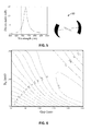
- FIG. 5 shows the directionality along the x-axis on a dB-scale, being 10 log(r), where r is the ratio of the scattered radiation transmitted through a spatial region on the left of the x-axis and the scattered radiation transmitted through a spatial region on the right of the x-axis, as shown in the illustration 30 in FIG. 5 .
- the directionality reaches a maximum of 15dB at 720nm for this specific example.
- FIG. 6 shows the maximum of directivity for a single split ring resonator for a constant R y as function of R x and G.
- the most directional ring is a ring with a small R x and a large gap. If the gap is reduced, R x needs to increase in order to reach optimal directivity.
- the first part 13 and the second part 14 are furthermore functionally connected in a linkage region 15.
- the electro conductor 12 is shaped such as to form a capacitive gap 16.
- the first part 13 and the second part 14 may each form an open loop, with the ends of this loop separated by a gap.
- the ends of the loop of the first part 13 and of the loop of the second part 14 may furthermore be connected one on one in the linkage region 15, such that the gap separating the ends of each loop is shared, being the capacitive gap 16.
- the gap is kept as small as possible in order to really have a high field, so that there is a strong interaction with the medium or a fluorophore therein.
- a trade off between optimal high field and directivity is to be made.
- the gap advantageously should be small enough so the structure can be treated as the combination of 2 C's.
- the resonance wavelengths can e.g. be tuned to the intended spectral domain by tuning particular dimensions of the structure, e.g. by tuning Rx and especially Ry.
- the electro conductor 12 is furthermore configured to direct the incident radiation of the first wavelength toward a first direction and to direct the incident radiation of the second wavelength toward a second direction, in which this first direction and this second direction are separated by an angle of at least 60°, for example, the first direction and the second direction may be substantially opposite spatial directions, e.g. may be opposite spatial directions.
- the plasmonic structure 10 may be used as a plasmonic antenna that emits radiation to the right or left side of the antenna depending on the wavelength, e.g. as a plasmonic wavelength selective switch.
- the radiation incident on the plasmonic structure may for example be scattered radiation from a perpendicular beam or fluorescent radiation from a quantum emitter placed at the centre of the antenna.
- measuring the degree of directionality by comparing the radiation collected at both sides of the antenna can advantageously also serve as a robust self-referenced measurement.
- Spectral information is immediately gained from the scattering pattern and can for example be used to detect a shift in refractive index of the medium surrounding the antenna in the case of scatted radiation, or to identify a fluorophore at the centre of the antenna.
- two split ring resonators e.g. with different R x and R y may be joined at the gap in embodiments according to the present invention.
- This type of resonator may scatter directionally to the left at one wavelength and scatter to the right at another.
- the resonators shape and the intended effect can be seen in FIG. 7 , showing a planar electromagnetic wave E with wave vector k which comprises components of the first and second wavelength that impinges onto the plasmonic structure according to embodiments and is split into two outgoing waves as function of the wavelength in two opposing directions.
- FIG. 8 shows the spectrum of this type of resonator.
- Two clear resonances, Q y1 and Q y2 can be seen in the absorption spectrum 33 at 715 nm and 810nm, respectively.
- the scattering 31 and extinction 32 spectrum show the clear asymmetry associated with Fano resonances. These resonances can be linked to the left and right part of the antenna.
- the charge plot 34 in FIG. 8 illustrates this. At the red side of both resonances directionality can be observed, as illustrated in the bottom plot 35 in FIG. 8 .
- the resonance at 715nm, associated with the left part of the resonator shows directionality to the right while the resonance at 810nm, associated with the right part of the resonator, shows directionality to the left.
- the double split ring resonator has also a low net dipole between the two dipole resonances of the left and right split ring resonator.
- the three low net dipole regions 44 where directional scattering might occur are schematically indicated in FIG. 11 .
- the dipole-dipole-region can also be used to tune the scatter directionally. To make this region accessible for visible wavelengths, the resonator can be scaled down. Advantages of using this region instead of the lower region are that it is easier to obtain good directionality when the antenna lies on a substrate and that it suffers much less from scattering in the Y-direction.
- FIG. 11 Advantages of using this region instead of the lower region are that it is easier to obtain good directionality when the antenna lies on a substrate and that it suffers much less from scattering in the Y-direction.
- the first part 13 and the second part 14 are furthermore functionally connected in a linkage region 15, where the electro conductor 12 is shaped such as to form a capacitive gap 16.
- the electro conductor 12 is shaped such as to form a capacitive gap 16.
- a fluorophore placed in or near the gap 16 may advantageously excite both the left or right part of the resonator, depending on its emission wavelength. This effect is schematically illustrated in FIG. 13 , in which short wavelength incoming radiation E with wave vector k excites the quantum emitter, and is directed to either direction depending on the fluorophore emission wavelength.
- FIG. 14 shows the total 51, non-radiative 52 and radiative 53 enhancement of the decay rate of a quantum emitter in or near the gap 16 of a plasmonic structure according to embodiments.
- the ratio 54 of the radiative and total decay rate is the quantum efficiency and is mapped on the right axis.
- the resonances of the plasmonic structure having a quantum emitter in or near the gap lie at a lower wavelength than for the plasmonic structure without quantum emitter discussed hereinabove.
- the simulation results depicted here were performed with an aluminium antenna instead of a gold one. This material change causes a blue shift making the resonances accessible for wider range of fluorophores.
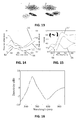
- FIG. 15 shows the contribution of the radiative decay rate that scattered to the left or to the right.
- the fluorophore excites the left part of the plasmonic structure and most of the radiation scatters to the right side 56.
- the right part is excited and radiation scatters to the left 55.
- the sum of both left scattered radiation 55 and right scattered radiation 56 is also shown in plot 57.
- the ratio of the left and right scattered radiation on a dB-scale is shown in FIG. 16 . Both resonances peak at about ⁇ 6dB.
- This changing emission pattern can be used to identify the quantum emitter at the centre.
- the antenna will emit the radiation in a certain left to right ratio. Since different fluorophores emit at a different wavelength, a quantum emitter can be identified by the left-right ratio.
- the capacitive gap 16 may therefore comprise a quantum emitter.
- the capacitive gap 16 may be functionalized to capture a quantum emitter, e.g. to capture at least one of a plurality of quantum emitter, e.g. fluorescently labelled bioparticles.
- the fluorophores do not emit in a single wavelength. They have a certain bandwidth. Because of this the total emitted radiation scattered to the left or the right is spread out.
- FIG. 17 the emitted radiation to the left and right side for four different dyes, AttoRho6G, PECF594, DY481XL and PerCP, is shown as function of the wavelength. The left and right scattered radiation was integrated and compared. In the case of the AttoRho6G dye, which emits around 560nm, almost double the amount of power is send to the left compared to the right, while for PerCP four times as much is send to the right compared to the left. In FIG. 18 , the fractions of left and right emitted radiation are shown. Every dye takes a specific place on the curve.
- the dipole-dipole region can also be used to cause directional emission. As discussed hereinabove, this is easier to obtain directional scattering for an antenna on glass.
- FIG. 19 shows the directivity 65 for a gold antenna on a glass substrate using this region, as well as radiative 68, non-radiative 66 and total enhancement 67 of the emission from a quantum emitter in the gap of the plasmonic structure. Directivity larger than 12dB is reached in both directions.
- FIG. 20 shows a plot of the intensity as captured by a detector positioned on the right 71 and on the left side 70.
- the present invention relates to a sensor comprising a plasmonic structure 10 according to embodiments of the first aspect of the present invention.
- FIG. 9 shows an exemplary compact sensor 100 according to embodiments of this second aspect of the present invention.
- This sensor further comprises a first radiation detection element 101 and a second radiation detection element 102.
- the plasmonic structure 10 is arranged such as to direct radiation E incident on the plasmonic structure of the first wavelength predominantly toward the first radiation detection element 101, and to direct radiation incident on the plasmonic structure of the second wavelength predominantly toward the second radiation detection element 102.
- the sensor may comprise a sample positioning means for bringing a sample into contact with the plasmonic structure.
- the sample positioning means may comprise a detection surface.
- Such a surface may be functionalised for capturing targets of interest. Functionalised surfaces are well known by the skilled person.
- the senor may be adapted for guiding an excitation beam towards the plasmonic structure.
- the sensor also may comprise an excitation source for generating an excitation beam.
- optical components and/or waveguides may be incorporated for guiding radiation to the structure.
- waveguides used for directing the fluorescence radiation towards the detection elements may also be used for directing the excitation radiation towards the plasmonic structure.
- the sensor may, amongst others in such cases, comprise a filter covering the first radiation detection element 101 and the second radiation detection element 102 for filtering out the portion of a excitation radiation.
- the sensor also may comprise a processor for processing radiation sensed at the first and/or second radiation detection element and/or for determining a ratio of the amount of radiation detected in the first radiation detection element and the amount of radiation detected in the second radiation detection element.
- a processor furthermore may be programmed for deriving therefrom a property of the sample under study.
- the plasmonic structure e.g. a double split ring antenna as described hereinabove, is arranged close to two detection regions, e.g. two detection elements for measuring the radiation.
- the sensor may comprise a filter covering the detection regions, which is adapted for filtering out the portion of an excitation beam incident the plasmonic structure that is transmitted through the plasmonic structure substantially unaffected.
- substantially only the high angle side scattering of the plasmonic structure may be detected by the detection regions.
- the resonance frequency can shift and a change in the left-right scattering ratio can be detected.
- a quantum emitter When a quantum emitter binds in the gap 16 it can be easily identified by the intensity ratio of the intensities measured by these detectors. This is illustrated in FIG. 21 .
- the darker regions represent the two detection regions and are shielded from the excitation beam by a filter.
- Almost all the radiation of a quantum emitter A is sent to the left detector, as shown in illustration 80
- most of the radiation of a quantum emitter B is sent to the left detector, as shown in illustration 81
- most of the radiation of an quantum emitter C is sent to the right detector, as shown in illustration 82
- almost all of the radiation of a quantum emitter D is sent to the right detector, as shown in illustration 83.
- the present invention relates to a method for wavelength selective switching of radiation.
- An exemplary method 200 according to embodiments of this third aspect of the invention is shown in FIG. 22 .
- the elements introduced during the corresponding method steps are shown in FIG. 23 , whereby for each element, the corresponding method step is indicated.
- the method 200 comprises providing 201 a plasmonic structure 10 comprising an electro conductor 12 which comprises a first part 13 configured to provide a first series of plasmon resonance modes for incident radiation (which result in directive radiation for a first wavelength) and a second part 14 configured to provide a second series of plasmon resonance modes for incident radiation (which result in directive radiation for a second wavelength), the first part 13 and second part 14 being functionally connected in a linkage region 15.
- the electro conductor 12 is furthermore configured to direct radiation incident on the plasmonic structure of a first wavelength predominantly toward a first direction and to direct radiation incident on the plasmonic structure of a second wavelength predominantly toward a second direction.
- providing 201 the plasmonic structure 10 may comprise providing a plasmonic structure 10 according to the first aspect of the present invention.
- the method 200 may also comprise introducing 203 a fluorophore in or near a capacitive gap 16 formed in the linkage region 15.
- the method comprises providing a sample with differently fluorescently labelled targets of interest.
- the fluorescent labels may be selected so that these emit at different wavelengths, the radiation being directed to different directions or in different proportions to different directions.
- the method thus may allow identifying different targets.
- the method may comprise exciting fluorophores by directing an excitation beam to the plasmonic structure.
- the method also can be used for identifying a change in a property of the material near the plasmonic structure, e.g. for identifying a refractive index change near the plasmonic structure.
- the refractive index change may be induced by binding of targets on a sensor surface at or near the plasmonic structure.
- the surface of the plasmonic structure may be functionalised for receiving the targets of interest. Functionalising a surface is a technique well known by the person skilled in the art and therefore is not further discussed here in detail.
- the method 200 further comprises impinging 202 a radiation wave onto the plasmonic structure such as to direct a first component of the radiation wave corresponding to the first wavelength toward the first direction and to direct a second component of the radiation wave corresponding to the second wavelength toward the second direction.
- the method 200 may also comprise determining 204 a radiative property, e.g. a radiation intensity, of the first component of the radiation wave and of the second component of the radiation wave.
- a radiative property e.g. a radiation intensity
- the method 200 may also comprise determining 205 a property of the fluorophore, for example identifying the fluorophore from a plurality of possible fluorophores, taking into account the determined radiative property of the first component and the second component.
Landscapes
- Physics & Mathematics (AREA)
- General Physics & Mathematics (AREA)
- Health & Medical Sciences (AREA)
- Engineering & Computer Science (AREA)
- Chemical & Material Sciences (AREA)
- Optics & Photonics (AREA)
- Immunology (AREA)
- Life Sciences & Earth Sciences (AREA)
- Microelectronics & Electronic Packaging (AREA)
- Analytical Chemistry (AREA)
- Biochemistry (AREA)
- General Health & Medical Sciences (AREA)
- Pathology (AREA)
- Nuclear Medicine, Radiotherapy & Molecular Imaging (AREA)
- Nanotechnology (AREA)
- Chemical Kinetics & Catalysis (AREA)
- Mathematical Physics (AREA)
- Theoretical Computer Science (AREA)
- Crystallography & Structural Chemistry (AREA)
- Investigating Or Analysing Materials By Optical Means (AREA)
Abstract
Description
- The invention relates to the field of surface plasmon resonance photonics. More specifically it relates to a plasmonic wavelength selective switch.
- It is known in the art that surface plasmon resonance in nano scale structures, such as nanoparticles, can be used for directing electromagnetic radiation in the visible spectrum in a manner similar to the directional transmission by radiofrequency antennas. For example, in the radiofrequency spectrum, a typical antenna design for high directivity is the Yagi-Uda antenna, which comprises a linear array of antenna elements, where an array of nanoparticles can provide a similar radiation pattern in the optical regime. Directional control of visible spectrum radiation can thus be obtained by a nano-optical Yagi-Uda antenna comprising, for example, an appropriately configured arrangement of gold nano rods.
- Plasmonic antennas may be useful components for microscopic or nano scale optical systems. For example, sending or receiving photons in a directionally selective fashion may find application in the field of micro- and nano scale photonics. By such directional sending or receiving of photons, signals may be transmitted in a well-defined direction or the signal to noise ratio of a detector may be increased by such directionally selective components. Furthermore, wavelength dependent directivity may be particularly advantageous for scaling sensors. Plasmonic sensors are usually based on detecting changes in the spectrum of radiation coming from an object of interest, e.g. scattered, transmitted or fluorescent radiation. Spectral information is typically recovered by gratings or filters. These components are large compared to plasmonic antennas, and furthermore hard to miniaturize. If the spectral information would already be present in the scatter or emission patterns coming from the antenna this can simplify spectral analysis, and thus may result in cheaper, more compact devices.
- The split ring resonator has been studied in the art as an artificial magnetic atom. It has also been shown, for example by Yao Jie et al. in "an antenna to direct radiation to opposite directions," Optics Communications 300, p. 274-276, that a split ring resonator can be used as an optical antenna to direct radiation emitted by an electric source to different directions at different wavelengths. This phenomenon, according to Jie et al., can be explained by a two-dipole model.
- It is an object of embodiments of the present invention to provide simple and efficient means and methods for selective switching different wavelengths of radiation into different spatial directions.
- It is an advantage of embodiments of the present invention that optical signals may be switched as function of their wavelength in a well-defined direction corresponding to that wavelength.
- It is an advantage of embodiments of the present invention that the signal to noise ratio of a detector may be increased by using a directionally selective component according to embodiments. It is a further advantage that small-scale nano-photonic integration can be achieved by embodiments of the present invention.
- It is an advantage of the present invention that the use of components according to the present invention in a nano-photonic device can lead to a cheap and compact device.
- It is an advantage of embodiments of the present invention that a functional structure for selective wavelength switching is provided that only requires few components, e.g. a single simple structure, and few different materials, e.g. a single electro conductor material provided in or on a single substrate material.
- It is an advantage of embodiments of the present invention that radiation of different wavelengths can be directed in more than one distinct wave-length specific direction.
- It is an advantage of embodiments of the present invention that directionality and wavelength dependence of a structure according to embodiments can be easily tuned.
- It is an advantage of embodiments of the present invention that a plasmonic structure is provided which show good interaction properties with quantum emitters.
- The above objective is accomplished by a method and device according to the present invention.
- The present invention relates to a plasmonic structure comprising a substrate and at least one electro conductor provided in or on the substrate, the at least one electro conductor comprising a first part configured to provide a first series of plasmon resonance modes for incident radiation - the incident radiation may results in directive radiation at a first wavelength - and a second part configured to provide a second series of plasmon resonance modes for incident radiation - the second part may result in directive radiation at a second wavelength -, the first part and second part being functionally connected in a linkage region, the electro conductor being shaped in said linkage region such as to form a capacitive gap, wherein the electro conductor is furthermore configured to direct radiation incident on the plasmonic structure of the first wavelength predominantly toward a first direction and to direct radiation incident on the plasmonic structure of the second wavelength predominantly toward a second direction, the first direction and the second direction being separated by an angle of at least 60°. It is an advantage of embodiments of the present invention to provide a plasmonic structure wherein dependent on the wavelength, incident radiation or fluorescent radiation that is created is guided into different directions.
- The first direction and said second direction may be substantially opposite spatial directions. It is an advantage of embodiments of the present invention that the radiation is emitted/scattered in distinct directions. It is an advantage of embodiments of the present invention that such directivity allows accurate more easy manufacturing, e.g. waveguides can more easily be defined in the structure.
- The first part may form a first plasmonic split ring resonator and the second part forms a second plasmonic split ring resonator. It is an advantage of embodiments of the present invention that efficient emission or scattering of radiation in distinct directions is obtained.
- The first plasmonic split ring resonator and the second plasmonic split ring resonator may each have an elliptical shape. The first plasmonic split ring resonator and the second plasmonic split ring resonator may have a block-like shape.
- The electro conductor may comprise a noble metal. It may comprise aluminum.
- The substrate may comprise glass.
- The substrate may form part of a waveguide in an integrated photonics system.
- The capacitive gap may comprise a quantum emitter or in which said capacitive gap is functionalized to capture a quantum emitter.
- The present invention also relates to a sensor comprising a plasmonic structure as described above, a first radiation detection element and a second radiation detection element the plasmonic structure being arranged such as to direct radiation incident on the plasmonic structure of the first wavelength predominantly toward the first radiation detection element, and to direct radiation incident on the plasmonic structure of the second wavelength predominantly toward the second radiation detection element. It is an advantage of embodiments of the present invention that a sensor can be obtained wherein the use of a grating for spectrally splitting incident or induced radiation can be avoided. It is an advantage of embodiments of the present invention that spectrally splitting radiation can be obtained using components with a small footprint, thus allowing miniaturization of the system.
- The sensor furthermore may comprise a filter covering the first radiation detection element and the second radiation detection element, the filter being adapted for filtering out the portion of a radiation wave incident on the plasmonic structure that is transmitted through the plasmonic structure substantially unaffected.
- The sensor may comprise a sample positioning means for bringing a sample into contact with the plasmonic structure. It is an advantage of embodiments according to the present invention that a sensor is provided for characterizing a sample. Such a sample may be a fluid although embodiments of the present invention are not limited thereto.
- The sensor may comprise an excitation source for exciting fluorescent labels being positioned near the plasmonic structure, the sensor furthermore being adapted for characterizing differently fluorescent labeled targets of interest in the sample. The sensor thus may allow to detect different targets of interest in the sample. The sample may be provided using a microfluidic channel.
- The sensor may comprise a processor for processing radiation sensed at the first and/or second radiation detection element and/or for determining a ratio of the amount of radiation detected in the first radiation detection element and the amount of radiation detected in the second radiation detection element. It is an advantage of embodiments according to the present invention that the ratio of the amounts of radiation detected in the different radiation detection elements can be used as discriminator to identify changes in the incident or induced radiation and thus in a sample to be characterized and brought into contact with the plasmonic structure.
- The present invention relates to a method for wavelength selective switching of radiation, the method comprising
providing a plasmonic structure comprising an electro conductor which comprises a first part configured to provide a first plasmon resonance mode for incident radiation of a first wavelength and a second part configured to provide a second plasmon resonance mode for incident radiation of a second wavelength, the first part and second part being functionally connected in a linkage region, wherein the electro conductor is furthermore configured to direct radiation incident on the plasmonic structure of the first wavelength predominantly toward a first direction and to direct radiation incident on the plasmonic structure of the second wavelength predominantly toward a second direction, and
impinging a radiation wave onto the plasmonic structure such as to direct a first component of said radiation wave corresponding to the first wavelength toward said first direction and to direct a second component of said radiation wave corresponding to the second wavelength toward the second direction.
The method further may comprise introducing a fluorophore in or near a capacitive gap formed in said linkage region,
determining a radiative property of said first component of said radiation wave and of said second component of said radiation wave, and
determining a property of said fluorophore taking into account the determined radiative property of the first component and the second component. - The method may comprise evaluating a ratio of the radiation directed to the first direction and the radiation directed to the second direction.
- Particular and preferred aspects of the invention are set out in the accompanying independent and dependent claims. Features from the dependent claims may be combined with features of the independent claims and with features of other dependent claims as appropriate and not merely as explicitly set out in the claims.
- These and other aspects of the invention will be apparent from and elucidated with reference to the embodiment(s) described hereinafter.
-
-
FIG. 1 shows a plasmonic structure according to embodiments of the present invention. -
FIG. 2 shows an exemplary single split ring resonator as known in the art, and a schematic representation of directional scattering of an incident planar wave by such resonator. -
FIG. 3 shows the extinction, scattering and absorption spectrum of a single split ring resonator, as known in the art, and a schematic representation of the Fano interference in such single split ring resonator. -
FIG. 4 illustrates the directional scattering by asymmetric constructive interference and destructive interference of two dipoles with a phase difference, Δφ, separated by a distance, d, in a single split ring resonator, as known in the art. -
FIG. 5 shows the directionality in logarithmic scale for a single split ring resonator, as known in the art, and illustrates the spatial regions which are used to collect the right and left scattered radiation on which this directionality measure is based. -
FIG. 6 show the maximal directionality reached in logarithmic scale as function of the radius Rx and the gap width, G, for a single split ring resonator known in the art with a 200nm γ-radius Rγ. -
FIG. 7 shows a schematic representation of the directional scattering of a plasmonic structure according to embodiments of the present invention. -
FIG. 8 shows extinction, scattering and absorption spectra of a plasmonic structure according to embodiments of the present invention, a charge plot of the plasmonic structure at the two resonances and the obtained directionality of the plasmonic structure. -
FIG. 9 shows an exemplary compact sensor using a plasmonic structure according to embodiments of the present invention. -
FIG. 10 shows different extinction spectra and corresponding directionality of plasmonic structures according to embodiments with a Ry1 of 250nm and a Ry2 of 275nm, 300nm and 325nm. -
FIG. 11 shows the net dipole contribution associated with the different resonances present in a plasmonic structure according to embodiments. -
FIG. 12 shows the directivity and radiative, absorption and extinction spectra of a plasmonic structure according to embodiments configured as a double C-antenna on glass. -
FIG. 13 shows a schematic representation of the directional emission at two different wavelengths for plasmonic structure according to embodiments having a fluorophore quantum emitter arranged in or near the gap. -
FIG. 14 shows total, non-radiative and radiative decay rate enhancement compared to the decay in free space for the plasmonic structure according to embodiments having a quantum emitter arranged in or near the gap. -
FIG. 15 shows the portion of the radiative decay rate associated with emission to the right, to the left and the sum of both for the plasmonic structure according to embodiments having a quantum emitter arranged in or near the gap. -
FIG. 16 shows the directivity in dB for the plasmonic structure according to embodiments having a quantum emitter arranged in or near the gap. -
FIG. 17 shows the radiation intensity emitted to the right and left in function of the wavelength for 4 different dyes placed in the central gap of a plasmonic structure according to embodiments. -
FIG. 18 shows the left-right power fraction for the four different dyes placed in the central gap of a plasmonic structure according to embodiments. -
FIG. 19 shows the directivity (units on right axis), and radiative, non-radiative and total enhancement of the emission (units on left axis) from a dye in the gap of a golden double C-shaped antenna on glass according to embodiments of the present invention. -
FIG. 20 shows the intensity captured by detectors positioned right and left for of the emission from a quantum emitter in the gap of a golden double C-shaped antenna on glass according to embodiments of the present invention. -
FIG. 21 shows Illustrations of a compact sensor according to embodiments of the present invention, where the left-right scatter ratio are used to identify the quantum emitter located in the gap of the plasmonic structure. -
FIG. 22 shows an exemplary method according to embodiments of the present invention. -
FIG. 23 shows the elements of a system and the corresponding method steps where the elements play an important role, according to an embodiment of the present invention. - The drawings are only schematic and are non-limiting. In the drawings, the size of some of the elements may be exaggerated and not drawn on scale for illustrative purposes.
- Any reference signs in the claims shall not be construed as limiting the scope.
- In the different drawings, the same reference signs refer to the same or analogous elements.
- The present invention will be described with respect to particular embodiments and with reference to certain drawings but the invention is not limited thereto but only by the claims. The drawings described are only schematic and are non-limiting. In the drawings, the size of some of the elements may be exaggerated and not drawn on scale for illustrative purposes. The dimensions and the relative dimensions do not correspond to actual reductions to practice of the invention.
- Furthermore, the terms first, second and the like in the description and in the claims, are used for distinguishing between similar elements and not necessarily for describing a sequence, either temporally, spatially, in ranking or in any other manner. It is to be understood that the terms so used are interchangeable under appropriate circumstances and that the embodiments of the invention described herein are capable of operation in other sequences than described or illustrated herein. Moreover, the terms top, under and the like in the description and the claims are used for descriptive purposes and not necessarily for describing relative positions. It is to be understood that the terms so used are interchangeable under appropriate circumstances and that the embodiments of the invention described herein are capable of operation in other orientations than described or illustrated herein.
- It is to be noticed that the term "comprising", used in the claims, should not be interpreted as being restricted to the means listed thereafter; it does not exclude other elements or steps. It is thus to be interpreted as specifying the presence of the stated features, integers, steps or components as referred to, but does not preclude the presence or addition of one or more other features, integers, steps or components, or groups thereof. Thus, the scope of the expression "a device comprising means A and B" should not be limited to devices consisting only of components A and B. It means that with respect to the present invention, the only relevant components of the device are A and B.
- Reference throughout this specification to "one embodiment" or "an embodiment" means that a particular feature, structure or characteristic described in connection with the embodiment is included in at least one embodiment of the present invention. Thus, appearances of the phrases "in one embodiment" or "in an embodiment" in various places throughout this specification are not necessarily all referring to the same embodiment, but may. Furthermore, the particular features, structures or characteristics may be combined in any suitable manner, as would be apparent to one of ordinary skill in the art from this disclosure, in one or more embodiments.
- Similarly it should be appreciated that in the description of exemplary embodiments of the invention, various features of the invention are sometimes grouped together in a single embodiment, figure, or description thereof for the purpose of streamlining the disclosure and aiding in the understanding of one or more of the various inventive aspects. This method of disclosure, however, is not to be interpreted as reflecting an intention that the claimed invention requires more features than are expressly recited in each claim. Rather, as the following claims reflect, inventive aspects lie in less than all features of a single foregoing disclosed embodiment. Thus, the claims following the detailed description are hereby expressly incorporated into this detailed description, with each claim standing on its own as a separate embodiment of this invention.
- Furthermore, while some embodiments described herein include some but not other features included in other embodiments, combinations of features of different embodiments are meant to be within the scope of the invention, and form different embodiments, as would be understood by those in the art. For example, in the following claims, any of the claimed embodiments can be used in any combination. In the description provided herein, numerous specific details are set forth. However, it is understood that embodiments of the invention may be practiced without these specific details. In other instances, well-known methods, structures and techniques have not been shown in detail in order not to obscure an understanding of this description.
- In a first aspect, the present invention relates to a plasmonic structure which comprises an electro conductor provided in or on a substrate. The electro conductor comprises a first part configured to provide a first series of plasmon resonance modes (for incident radiation which result in directive radiation for a first wavelength) and the electro conductor also comprises a second part configured to provide a second series of plasmon resonance modes (for incident radiation which result in directive radiation for a second wavelength). The first part and the second part are furthermore functionally connected in a linkage region. In this linkage region, the electro conductor is shaped such as to form a capacitive gap. The electro conductor is furthermore configured to direct radiation incident on the plasmonic structure of a first wavelength predominantly toward a first direction and to direct radiation incident on the plasmonic structure of a second wavelength predominantly toward a second direction, in which this first direction and this second direction are separated by an angle of at least 60°, for example in which the first direction and the second direction are substantially opposite spatial directions, e.g. are opposite spatial directions.
- Standard and optional features will further be described with reference to
FIG. 1 , illustrating an example of a structure according to the present invention, although embodiments are not limited thereto. - Referring to
FIG. 1 , aplasmonic structure 10 according to embodiments of the present invention is shown. Theplasmonic structure 10 may comprise asubstrate 11, e.g. an optical substrate such as a silicon, silicon nitride or silicon dioxide substrate, e.g. a silicon-on-insulator substrate. Thesubstrate 11 may for example comprise glass, e.g. the substrate may be a glass substrate. - However, in embodiments according to the present invention, the
substrate 11 may form part of a waveguide in an integrated photonics system. It is an advantage of such embodiments that theplasmonic structure 10 can be sufficiently small to be, for example, integrated in the top cladding of a waveguide structure. Theplasmonic structure 10 may advantageously direct radiation of the first wavelength towards one direction of the waveguide, and radiation of the second wavelength towards the other direction of the waveguide, thus avoiding or complementing conventional spectral switching means, such as diffractive gratings. - The
plasmonic structure 10 comprises anelectro conductor 12 provided in or on thesubstrate 11.Such electro conductor 12 may comprise an electrically conducting medium suitable for surface plasmon resonance structures, for example a metallic material such as a noble metal, e.g. gold or silver, or aluminium. For example, theelectro conductor 12 may be a semi-transparent noble metal provided on the substrate in a patterned coating.Such electro conductor 12 may be provided onto the substrate under conditions of total internal reflection, e.g. such that a condition of total internal reflection exists at the interface. The thickness of the noble metal layer, e.g. gold, that can be used may in one example be about 50nm. Typically the thickness of these kind of structures can vary between 20nm and 100nm. In one example, the width may be between 40nm and 60nm, depending on the thickness of the end material that can be reached. Typically, the width of the structure may vary between 20nm and 200nm. - The
electro conductor 12 comprises afirst part 13 configured to provide a first series of plasmon resonance modes for incident radiation (which result in directive radiation at a first wavelength). Furthermore, the electro conductor comprises asecond part 14 configured to provide a second series of plasmon resonance modes for incident radiation (which causes directive radiation at a second wavelength). Particularly, the plasmon resonance modes associated with first part and the plasmon resonance modes associated with the second part may have peak resonance wavelengths which are clearly distinct, e.g. which leads to separation of the first and second wavelengths by at least 50 nm, e.g. by at least 100 nm. - The
first part 13 may form a first plasmonic split ring resonator and the second part may form a second plasmonic split ring resonator, e.g. thefirst part 13 and thesecond part 14 each in isolation have the shape and configuration of a plasmonic split ring resonator, e.g. as known to the person skilled in the art. Although the first plasmonic split ring resonator and/or the second split ring resonator may have any shape as known for surface plasmon split ring resonators in the art, e.g. rectangular or circular, in a preferred embodiment, the first plasmonic split ring resonator and the second plasmonic split ring resonator may each have an elliptical shape. However, in preferred embodiments, the first plasmonic split ring resonator and the second plasmonic split ring resonator may differ in shape and/or dimensions, such as to provide a substantial difference in the peak resonance wavelengths of the first plasmon resonance modes and the second plasmon resonance modes. - In order to provide some insights in how a plasmonic split ring resonator operates, some further description is provided below.
- In
FIG. 2 such a plasmonic split ring resonator, e.g. forming thefirst part 13 orsecond part 14 in a structure according to embodiments, is shown in isolation. Directionality in one direction can be obtained by a single split ring resonator, as illustrated by the schematic representation of the scattering of an incident planar electromagnetic wave E having wave vector k inFIG. 2 . The ring may be generally elliptical in shape with a capacitive gap defined in the ring. Such ring can be defined by a radius along the x-axis, Rx, a radius along the y-axis, Ry, and a width, G, of the capacitive gap provided between the open ends of the split ring. Theextinction 21, scattering 22 andabsorption 23 spectrum of such an exemplary resonator for y-polarized radiation between 600nm and 900 nm is shown inFIG. 3 . At 690nm, the quadrupole resonance, Qy, can be seen. It lies in the tail of a dipole resonance, Dy, which has a wavelength above 900nm. A schematic representation of the charge of these plasmonic modes can be seen in theinsets FIG. 3 . Since both the resonances are Y-polarized, they can be exited by the same incoming radiation beam and will interfere. This type of interference is known as a Fano interference and can be recognized in the spectra by an asymmetric resonance scattering peak. In the case of this exemplary split ring resonator, increased scattering is observed below the resonance wavelength and reduced scattering is seen above the resonance wavelength. This asymmetry can be explained byconstructive interference 24 anddestructive interference 25 between Qy and Dy on respective sides of the peak. Below the spectral graph inFIG. 3 , the net dipole contributions of the two modes are schematically depicted along the spectra. For the Dy-resonance 28, the intensity decreases with decreasing wavelength and the phase relative to the incoming beam is relatively constant. The net dipole contribution of the Qy resonance 29 is largest around the resonance wavelength. In addition there is a phase change at the resonance wavelength. Thus the asymmetry may be explained. On the left side both the resonances are in phase and they interfere constructively, causing a large dipole and increased scattering. On the right side the resonances are out of phase and so they interfere destructively, causing a small dipole and decreased scattering. - In the spectral region on the right side of the Qy resonance, where the net dipole is small to non-existing, scattering is the result of the phase difference of the different dipoles as indicated in the Qy inset 26. Radiation in a certain direction in this case is dependent on the phase difference, Δφ, and the spatial distance, d, between the dipoles seen in this direction. When the phase difference matches the spatial distance, the radiation in a direction can be eliminated by destructive interference in one direction while being quite large, due to constructive interference, in the opposite direction. In other words at the right side of the resonance, thus the red side of the spectrum, the absence of a net dipole can lead to high directionality if d and Δφ match. This effect is depicted in
FIG. 4 . -
FIG. 5 shows the directionality along the x-axis on a dB-scale, being 10 log(r), where r is the ratio of the scattered radiation transmitted through a spatial region on the left of the x-axis and the scattered radiation transmitted through a spatial region on the right of the x-axis, as shown in theillustration 30 inFIG. 5 . The directionality reaches a maximum of 15dB at 720nm for this specific example. - In order to reach good directivity, both the ellipticity of the ring and the gap width may be tuned.
FIG. 6 shows the maximum of directivity for a single split ring resonator for a constant Ry as function of Rx and G. The most directional ring is a ring with a small Rx and a large gap. If the gap is reduced, Rx needs to increase in order to reach optimal directivity. - In the
plasmonic structure 10 according to embodiments of the present invention shown inFIG. 1 , thefirst part 13 and thesecond part 14 are furthermore functionally connected in alinkage region 15. In this linkage region, theelectro conductor 12 is shaped such as to form acapacitive gap 16. For example, thefirst part 13 and thesecond part 14 may each form an open loop, with the ends of this loop separated by a gap. The ends of the loop of thefirst part 13 and of the loop of thesecond part 14 may furthermore be connected one on one in thelinkage region 15, such that the gap separating the ends of each loop is shared, being the capacitive gap 16._Advantageously, the gap is kept as small as possible in order to really have a high field, so that there is a strong interaction with the medium or a fluorophore therein. However, as can be derived fromFIG. 6 , a trade off between optimal high field and directivity is to be made. Furthermore, the gap advantageously should be small enough so the structure can be treated as the combination of 2 C's. The resonance wavelengths can e.g. be tuned to the intended spectral domain by tuning particular dimensions of the structure, e.g. by tuning Rx and especially Ry. - Regarding the size off the antenna. It can actually be relatively large, for example up to Dy2=500nm which is almost in the range of the wavelength. This is why using the dipole/dipole region is actually also interesting. In order to use the dipole-dipole region one needs to make the antenna small.
- The
electro conductor 12 is furthermore configured to direct the incident radiation of the first wavelength toward a first direction and to direct the incident radiation of the second wavelength toward a second direction, in which this first direction and this second direction are separated by an angle of at least 60°, for example, the first direction and the second direction may be substantially opposite spatial directions, e.g. may be opposite spatial directions. - Thus, the
plasmonic structure 10 may be used as a plasmonic antenna that emits radiation to the right or left side of the antenna depending on the wavelength, e.g. as a plasmonic wavelength selective switch. The radiation incident on the plasmonic structure may for example be scattered radiation from a perpendicular beam or fluorescent radiation from a quantum emitter placed at the centre of the antenna. Apart from using this directionality to filter radiation or to send it out in a certain direction, measuring the degree of directionality by comparing the radiation collected at both sides of the antenna can advantageously also serve as a robust self-referenced measurement. Spectral information is immediately gained from the scattering pattern and can for example be used to detect a shift in refractive index of the medium surrounding the antenna in the case of scatted radiation, or to identify a fluorophore at the centre of the antenna. - Having discussed the directionality in a single split ring resonator, e.g. the
first part 13 or thesecond part 14 in isolation, two split ring resonators, e.g. with different Rx and Ry may be joined at the gap in embodiments according to the present invention. This type of resonator may scatter directionally to the left at one wavelength and scatter to the right at another. The resonators shape and the intended effect can be seen inFIG. 7 , showing a planar electromagnetic wave E with wave vector k which comprises components of the first and second wavelength that impinges onto the plasmonic structure according to embodiments and is split into two outgoing waves as function of the wavelength in two opposing directions. -
FIG. 8 shows the spectrum of this type of resonator. Two clear resonances, Qy1 and Qy2, can be seen in theabsorption spectrum 33 at 715 nm and 810nm, respectively. Thescattering 31 andextinction 32 spectrum show the clear asymmetry associated with Fano resonances. These resonances can be linked to the left and right part of the antenna. Thecharge plot 34 inFIG. 8 illustrates this. At the red side of both resonances directionality can be observed, as illustrated in thebottom plot 35 inFIG. 8 . The resonance at 715nm, associated with the left part of the resonator, shows directionality to the right while the resonance at 810nm, associated with the right part of the resonator, shows directionality to the left. - It is to be noted that this is opposite to what is seen in the single split ring resonator. A single split ring resonator with a gap on the right side scatters to the left. Yet the resonance at 715nm, scatters to the right. The combination with another split ring resonator may cause a change in the phase of the resonances that build up the scatter pattern, see
FIG. 4 . However, the red spectrum side of the resonances stays a region with a low net dipole moment. Thus, by tuning Rx and G, directionality can still be reached, albeit in the other direction. By tuning Ry1 and Ry2 the spectral position of the resonances can be changed. Increasing Ry red shifts the resonance. By decreasing the difference between Ry1 and Ry2, the resonances can thus be pushed closer together. The spectra and the directionality for a double C resonator with different Ry2 can be seen inFIG. 10 . When the resonances are very close together the directionality starts to decrease. InFIG 10 , different extinction spectra and corresponding directionality of double split ring resonators according to embodiments are shown with a Ry1 of 250nm and a Ry2 of 275nm inplot 41, of 300nm inplot 42 and 325nm inplot 43. - In addition to the two regions with a low net dipole that are present also in the single split ring resonator, the double split ring resonator has also a low net dipole between the two dipole resonances of the left and right split ring resonator. The three low
net dipole regions 44 where directional scattering might occur are schematically indicated inFIG. 11 . The dipole-dipole-region can also be used to tune the scatter directionally. To make this region accessible for visible wavelengths, the resonator can be scaled down. Advantages of using this region instead of the lower region are that it is easier to obtain good directionality when the antenna lies on a substrate and that it suffers much less from scattering in the Y-direction.FIG. 12 shows the radiative 47,absorption 46 andextinction 48 spectra and thedirectivity 45 for a gold double split ring resonator antenna on a glass substrate tuned for optimal directionality. In theplasmonic structure 10 according to embodiments of the present invention, thefirst part 13 and thesecond part 14 are furthermore functionally connected in alinkage region 15, where theelectro conductor 12 is shaped such as to form acapacitive gap 16. nFrom thecharge plot 34 inFIG. 8 , it can be seen that for both resonances charge accumulates at thegap 16, causing a high electric field in this central region. A fluorophore placed in or near thegap 16 may advantageously excite both the left or right part of the resonator, depending on its emission wavelength. This effect is schematically illustrated inFIG. 13 , in which short wavelength incoming radiation E with wave vector k excites the quantum emitter, and is directed to either direction depending on the fluorophore emission wavelength. -
FIG. 14 shows the total 51, non-radiative 52 and radiative 53 enhancement of the decay rate of a quantum emitter in or near thegap 16 of a plasmonic structure according to embodiments. Theratio 54 of the radiative and total decay rate is the quantum efficiency and is mapped on the right axis. It is to be noted that the resonances of the plasmonic structure having a quantum emitter in or near the gap lie at a lower wavelength than for the plasmonic structure without quantum emitter discussed hereinabove. The simulation results depicted here were performed with an aluminium antenna instead of a gold one. This material change causes a blue shift making the resonances accessible for wider range of fluorophores. -
FIG. 15 shows the contribution of the radiative decay rate that scattered to the left or to the right. At 570nm, the fluorophore excites the left part of the plasmonic structure and most of the radiation scatters to theright side 56. At 690m, the right part is excited and radiation scatters to the left 55. The sum of both leftscattered radiation 55 and rightscattered radiation 56 is also shown inplot 57. The ratio of the left and right scattered radiation on a dB-scale is shown inFIG. 16 . Both resonances peak at about ±6dB. - This changing emission pattern can be used to identify the quantum emitter at the centre. Depending on the wavelength of the emitted radiation by the quantum emitter the antenna will emit the radiation in a certain left to right ratio. Since different fluorophores emit at a different wavelength, a quantum emitter can be identified by the left-right ratio.
- In embodiments according to the present invention, the
capacitive gap 16 may therefore comprise a quantum emitter. Alternatively, thecapacitive gap 16 may be functionalized to capture a quantum emitter, e.g. to capture at least one of a plurality of quantum emitter, e.g. fluorescently labelled bioparticles. - However, the fluorophores do not emit in a single wavelength. They have a certain bandwidth. Because of this the total emitted radiation scattered to the left or the right is spread out. In
FIG. 17 , the emitted radiation to the left and right side for four different dyes, AttoRho6G, PECF594, DY481XL and PerCP, is shown as function of the wavelength. The left and right scattered radiation was integrated and compared. In the case of the AttoRho6G dye, which emits around 560nm, almost double the amount of power is send to the left compared to the right, while for PerCP four times as much is send to the right compared to the left. InFIG. 18 , the fractions of left and right emitted radiation are shown. Every dye takes a specific place on the curve. - Just as discussed for directional scattering without quantum emitter interaction in the plasmonic structure's gap, the dipole-dipole region can also be used to cause directional emission. As discussed hereinabove, this is easier to obtain directional scattering for an antenna on glass.
FIG. 19 shows thedirectivity 65 for a gold antenna on a glass substrate using this region, as well as radiative 68, non-radiative 66 and total enhancement 67 of the emission from a quantum emitter in the gap of the plasmonic structure. Directivity larger than 12dB is reached in both directions. -
FIG. 20 shows a plot of the intensity as captured by a detector positioned on the right 71 and on the left side 70. - In a second aspect, the present invention relates to a sensor comprising a
plasmonic structure 10 according to embodiments of the first aspect of the present invention.FIG. 9 shows an exemplarycompact sensor 100 according to embodiments of this second aspect of the present invention. This sensor further comprises a firstradiation detection element 101 and a secondradiation detection element 102. Theplasmonic structure 10 is arranged such as to direct radiation E incident on the plasmonic structure of the first wavelength predominantly toward the firstradiation detection element 101, and to direct radiation incident on the plasmonic structure of the second wavelength predominantly toward the secondradiation detection element 102. - The sensor may comprise a sample positioning means for bringing a sample into contact with the plasmonic structure. The sample positioning means may comprise a detection surface. Such a surface may be functionalised for capturing targets of interest. Functionalised surfaces are well known by the skilled person.
- In embodiments where fluorescence is used, the sensor may be adapted for guiding an excitation beam towards the plasmonic structure. The sensor also may comprise an excitation source for generating an excitation beam. Furthermore optical components and/or waveguides may be incorporated for guiding radiation to the structure. In some embodiments waveguides used for directing the fluorescence radiation towards the detection elements may also be used for directing the excitation radiation towards the plasmonic structure. The sensor may, amongst others in such cases, comprise a filter covering the first
radiation detection element 101 and the secondradiation detection element 102 for filtering out the portion of a excitation radiation. - The sensor also may comprise a processor for processing radiation sensed at the first and/or second radiation detection element and/or for determining a ratio of the amount of radiation detected in the first radiation detection element and the amount of radiation detected in the second radiation detection element. Such a processor furthermore may be programmed for deriving therefrom a property of the sample under study.
- In one embodiment, the plasmonic structure, e.g. a double split ring antenna as described hereinabove, is arranged close to two detection regions, e.g. two detection elements for measuring the radiation. Furthermore, the sensor may comprise a filter covering the detection regions, which is adapted for filtering out the portion of an excitation beam incident the plasmonic structure that is transmitted through the plasmonic structure substantially unaffected. Thus, substantially only the high angle side scattering of the plasmonic structure may be detected by the detection regions. Furthermore, when the refractive index of the medium changes due to analytes binding to the plasmonic structure, for example the resonance frequency can shift and a change in the left-right scattering ratio can be detected.
- When a quantum emitter binds in the
gap 16 it can be easily identified by the intensity ratio of the intensities measured by these detectors. This is illustrated inFIG. 21 . The darker regions represent the two detection regions and are shielded from the excitation beam by a filter. Almost all the radiation of a quantum emitter A is sent to the left detector, as shown inillustration 80, most of the radiation of a quantum emitter B is sent to the left detector, as shown inillustration 81, most of the radiation of an quantum emitter C is sent to the right detector, as shown inillustration 82, and almost all of the radiation of a quantum emitter D is sent to the right detector, as shown inillustration 83. - In a third aspect, the present invention relates to a method for wavelength selective switching of radiation. An
exemplary method 200 according to embodiments of this third aspect of the invention is shown inFIG. 22 . The elements introduced during the corresponding method steps are shown inFIG. 23 , whereby for each element, the corresponding method step is indicated. Themethod 200 comprises providing 201 aplasmonic structure 10 comprising anelectro conductor 12 which comprises afirst part 13 configured to provide a first series of plasmon resonance modes for incident radiation ( which result in directive radiation for a first wavelength) and asecond part 14 configured to provide a second series of plasmon resonance modes for incident radiation (which result in directive radiation for a second wavelength), thefirst part 13 andsecond part 14 being functionally connected in alinkage region 15. Theelectro conductor 12 is furthermore configured to direct radiation incident on the plasmonic structure of a first wavelength predominantly toward a first direction and to direct radiation incident on the plasmonic structure of a second wavelength predominantly toward a second direction. Particularly, providing 201 theplasmonic structure 10 may comprise providing aplasmonic structure 10 according to the first aspect of the present invention. - The
method 200 may also comprise introducing 203 a fluorophore in or near acapacitive gap 16 formed in thelinkage region 15. In one embodiment, the method comprises providing a sample with differently fluorescently labelled targets of interest. The fluorescent labels may be selected so that these emit at different wavelengths, the radiation being directed to different directions or in different proportions to different directions. The method thus may allow identifying different targets. The method may comprise exciting fluorophores by directing an excitation beam to the plasmonic structure. Alternatively, the method also can be used for identifying a change in a property of the material near the plasmonic structure, e.g. for identifying a refractive index change near the plasmonic structure. The refractive index change may be induced by binding of targets on a sensor surface at or near the plasmonic structure. In order to identify targets of interest in a sample, the surface of the plasmonic structure may be functionalised for receiving the targets of interest. Functionalising a surface is a technique well known by the person skilled in the art and therefore is not further discussed here in detail. - The
method 200 further comprises impinging 202 a radiation wave onto the plasmonic structure such as to direct a first component of the radiation wave corresponding to the first wavelength toward the first direction and to direct a second component of the radiation wave corresponding to the second wavelength toward the second direction. - The
method 200 may also comprise determining 204 a radiative property, e.g. a radiation intensity, of the first component of the radiation wave and of the second component of the radiation wave. - The
method 200 may also comprise determining 205 a property of the fluorophore, for example identifying the fluorophore from a plurality of possible fluorophores, taking into account the determined radiative property of the first component and the second component.
Claims (15)
- A plasmonic structure (10) comprising a substrate (11) and at least one electro conductor (12) provided in or on the substrate (11), the at least one electro conductor (12) comprising a first part (13) configured to provide a first series of plasmon resonance modes for incident radiation and a second part (14) configured to provide a second series of plasmon resonance modes for incident radiation, the first part (13) and second part (14) being functionally connected in a linkage region (15), the electro conductor (12) being shaped in said linkage region (15) such as to form a capacitive gap (16), wherein the electro conductor (12) is furthermore configured to direct radiation incident on the plasmonic structure of the first wavelength predominantly toward a first direction and to direct radiation incident on the plasmonic structure of the second wavelength predominantly toward a second direction, the first direction and the second direction being separated by an angle of at least 60°.
- The plasmonic structure according to claim 1, wherein said first direction and said second direction are substantially opposite spatial directions.
- The plasmonic structure according to claim 1 or claim 2, wherein the first part (13) forms a first plasmonic split ring resonator and the second part (14) forms a second plasmonic split ring resonator.
- The plasmonic structure according to claim 3, wherein the first plasmonic split ring resonator and the second plasmonic split ring resonator each have an elliptical shape.
- The plasmonic structure according to any of the previous claims, wherein said substrate (11) comprises glass.
- The plasmonic structure according to any of the previous claims, wherein said substrate (11) forms part of a waveguide in an integrated photonics system.
- The plasmonic structure according to any of the previous claims, wherein said capacitive gap (16) comprises a quantum emitter or in which said capacitive gap (16) is functionalized to capture a quantum emitter.
- A sensor (100) comprising a plasmonic structure (10) according to any of the previous claims, a first radiation detection element (101) and a second radiation detection element (102), the plasmonic structure (10) being arranged such as to direct radiation incident on the plasmonic structure of the first wavelength predominantly toward the first radiation detection element (101), and to direct radiation incident on the plasmonic structure of the second wavelength predominantly toward the second radiation detection element (102).
- The sensor (100) according to claim 8, furthermore comprising a filter covering the first radiation detection element (101) and the second radiation detection element (102), the filter being adapted for filtering out the portion of a radiation wave incident on the plasmonic structure that is transmitted through the plasmonic structure substantially unaffected.
- The sensor (100) according to any of claims 8 to 9, wherein the sensor comprises a sample positioning means for bringing a sample into contact with the plasmonic structure.
- The sensor (100) according to any of claims 8 or 10, the sensor comprising an excitation source for exciting fluorescent labels being positioned near the plasmonic structure, the sensor furthermore being adapted for characterizing differently fluorescent labeled targets of interest in the sample.
- The sensor (100) according to any of claims 8 to 11, the sensor comprising a processor for processing radiation sensed at the first and/or second radiation detection element and/or for determining a ratio of the amount of radiation detected in the first radiation detection element and the amount of radiation detected in the second radiation detection element.
- A method (200) for wavelength selective switching of radiation, the method comprising:- providing (201) a plasmonic structure (10) comprising an electro conductor (12) which comprises a first part (13) configured to provide a first plasmon resonance mode for incident radiation of a first wavelength and a second part (14) configured to provide a second plasmon resonance mode for incident radiation of a second wavelength, the first part (13) and second part (14) being functionally connected in a linkage region (15), wherein the electro conductor (12) is furthermore configured to direct radiation incident on the plasmonic structure of the first wavelength predominantly toward a first direction and to direct radiation incident on the plasmonic structure of the second wavelength predominantly toward a second direction, and- impinging (202) a radiation wave onto the plasmonic structure such as to direct a first component of said radiation wave corresponding to the first wavelength toward said first direction and to direct a second component of said radiation wave corresponding to the second wavelength toward the second direction.
- The method according to claim 13, furthermore comprising:- introducing (203) a fluorophore in or near a capacitive gap (16) formed in said linkage region (15),- determining (204) a radiative property of said first component of said radiation wave and of said second component of said radiation wave, and- determining (205) a property of said fluorophore taking into account the determined radiative property of the first component and the second component.
- The method according to any of claims 13 to 14, the method comprising evaluating a ratio of the radiation directed to the first direction and the radiation directed to the second direction.
Priority Applications (2)
| Application Number | Priority Date | Filing Date | Title |
|---|---|---|---|
| EP13197308.3A EP2884260B1 (en) | 2013-12-14 | 2013-12-14 | Plasmonic wavelength selective switch |
| US14/570,608 US9261648B2 (en) | 2013-12-14 | 2014-12-15 | Plasmonic wavelength selective switch |
Applications Claiming Priority (1)
| Application Number | Priority Date | Filing Date | Title |
|---|---|---|---|
| EP13197308.3A EP2884260B1 (en) | 2013-12-14 | 2013-12-14 | Plasmonic wavelength selective switch |
Publications (2)
| Publication Number | Publication Date |
|---|---|
| EP2884260A1 true EP2884260A1 (en) | 2015-06-17 |
| EP2884260B1 EP2884260B1 (en) | 2019-09-04 |
Family
ID=49880408
Family Applications (1)
| Application Number | Title | Priority Date | Filing Date |
|---|---|---|---|
| EP13197308.3A Not-in-force EP2884260B1 (en) | 2013-12-14 | 2013-12-14 | Plasmonic wavelength selective switch |
Country Status (2)
| Country | Link |
|---|---|
| US (1) | US9261648B2 (en) |
| EP (1) | EP2884260B1 (en) |
Cited By (3)
| Publication number | Priority date | Publication date | Assignee | Title |
|---|---|---|---|---|
| EP3223047A1 (en) * | 2016-03-25 | 2017-09-27 | IMEC vzw | Integrated dielectric optical nanoantenna |
| CN111175864A (en) * | 2019-12-22 | 2020-05-19 | 南京理工大学 | A Surface Plasmon Lens with a Cross Wire Array Structure |
| CN112881339A (en) * | 2021-01-12 | 2021-06-01 | 东北林业大学 | Solution concentration sensor of lateral coupling waveguide resonant cavity based on Fano resonance |
Families Citing this family (3)
| Publication number | Priority date | Publication date | Assignee | Title |
|---|---|---|---|---|
| CN107121793B (en) * | 2017-06-26 | 2018-08-07 | 南华大学 | A kind of surface plasma photoswitch based on periodical array of subwavelength holes |
| JP2019052854A (en) * | 2017-09-12 | 2019-04-04 | 株式会社東芝 | Radiation detection apparatus and radiation detection method |
| WO2020150743A1 (en) * | 2019-01-19 | 2020-07-23 | Northeastern University | Zero power micromechanical switch-based sensing and monitoring system |
Family Cites Families (2)
| Publication number | Priority date | Publication date | Assignee | Title |
|---|---|---|---|---|
| FR2931560B1 (en) * | 2008-05-20 | 2010-08-27 | Commissariat Energie Atomique | LIGHT FOCUSING DEVICE HAVING HIGH EFFICIENCY WAVE SUB-LENGTH DIMENSIONS |
| US8492737B2 (en) * | 2010-11-18 | 2013-07-23 | The Arizona Board Of Regents On Behalf Of The University Of Arizona | Tunable infrared emitter |
-
2013
- 2013-12-14 EP EP13197308.3A patent/EP2884260B1/en not_active Not-in-force
-
2014
- 2014-12-15 US US14/570,608 patent/US9261648B2/en not_active Expired - Fee Related
Non-Patent Citations (4)
| Title |
|---|
| S. H. ALAVI LAVASANI ET AL: "Color-switched directional ultracompact optical nanoantennas", JOURNAL OF THE OPTICAL SOCIETY OF AMERICA B, vol. 29, no. 6, 30 March 2012 (2012-03-30), pages 1361 - 3120, XP055106948, ISSN: 0740-3224, DOI: 10.1364/JOSAB.29.001361 * |
| TIMUR SHEGAI ET AL: "A bimetallic nanoantenna for directional colour routing", NATURE COMMUNICATIONS, vol. 2, 481, 20 September 2011 (2011-09-20), pages 1 - 6, XP055106927, DOI: 10.1038/ncomms1490 * |
| YAO JIE ET AL.: "an antenna to direct radiation to opposite directions", OPTICS COMMUNICATIONS, vol. 300, pages 274 - 276, XP055106885, DOI: doi:10.1016/j.optcom.2013.02.070 |
| YAO JIE ET AL: "An antenna to direct light to opposite directions", OPTICS COMMUNICATIONS, vol. 300, 20 March 2013 (2013-03-20), pages 274 - 276, XP055106885, ISSN: 0030-4018, DOI: 10.1016/j.optcom.2013.02.070 * |
Cited By (5)
| Publication number | Priority date | Publication date | Assignee | Title |
|---|---|---|---|---|
| EP3223047A1 (en) * | 2016-03-25 | 2017-09-27 | IMEC vzw | Integrated dielectric optical nanoantenna |
| US9927559B2 (en) | 2016-03-25 | 2018-03-27 | Imec Vzw | Wavelength-controlled directivity of all-dielectric optical nano-antennas |
| CN111175864A (en) * | 2019-12-22 | 2020-05-19 | 南京理工大学 | A Surface Plasmon Lens with a Cross Wire Array Structure |
| CN111175864B (en) * | 2019-12-22 | 2022-02-18 | 南京理工大学 | Surface plasmon lens of cross annular array structure |
| CN112881339A (en) * | 2021-01-12 | 2021-06-01 | 东北林业大学 | Solution concentration sensor of lateral coupling waveguide resonant cavity based on Fano resonance |
Also Published As
| Publication number | Publication date |
|---|---|
| US9261648B2 (en) | 2016-02-16 |
| EP2884260B1 (en) | 2019-09-04 |
| US20150168648A1 (en) | 2015-06-18 |
Similar Documents
| Publication | Publication Date | Title |
|---|---|---|
| US9261648B2 (en) | Plasmonic wavelength selective switch | |
| US9488583B2 (en) | Molecular analysis device | |
| JP7144730B2 (en) | diamond sensor system | |
| US8837039B2 (en) | Multiscale light amplification structures for surface enhanced Raman spectroscopy | |
| US20090310133A1 (en) | Method for designing light transmission device, optical element and sensor | |
| CA2912304A1 (en) | Structural colorimetric sensor | |
| JP2012522235A (en) | Waveguide integrated photodetector | |
| CN221613011U (en) | Magnetic sensor and weak magnetic detection system based on NV color center | |
| US9952453B2 (en) | Broadband metacoaxial optical nanoantennas based on plasmonic modes | |
| US20070030481A1 (en) | Molecular detector arrangement | |
| EP3223047A1 (en) | Integrated dielectric optical nanoantenna | |
| US9146235B2 (en) | Integrated fluorescence detection | |
| US20200056997A1 (en) | Simple sensing method employing raman scattering | |
| CN101346621B (en) | Luminescence sensor working in reflective mode | |
| US8395768B2 (en) | Scattering spectroscopy apparatus and method employing a guided mode resonance (GMR) grating | |
| US8472018B2 (en) | Grating for multiple discrete wavelengths of Raman scattering | |
| US10571398B2 (en) | Device for the beaming of light emitted by light sources, in particular fluorescence of molecules | |
| CN111830009A (en) | All-dielectric metasurface integrated Raman spectroscopy detection system | |
| CN107192675B (en) | Light modulation reflection spectrum detection system capable of simply and effectively inhibiting fluorescence interference | |
| WO2020053367A1 (en) | Calibration standard for evanescence microscopy | |
| La Spada et al. | Metamaterial resonator arrays for organic and inorganic compound sensing | |
| KR101222700B1 (en) | Surface plasmon resonance system device | |
| Martin et al. | Multichromatic illumination for smartphone biosensing using porous silicon rugate filters: role of width and spectral position of illumination peaks | |
| US20200182794A1 (en) | Biosensor using wire-grid polarizers for increasing cavity energy | |
| Tang | Silicon based photonic crystal coupled to an optical cavity for highly sensitive biodetection |
Legal Events
| Date | Code | Title | Description |
|---|---|---|---|
| PUAI | Public reference made under article 153(3) epc to a published international application that has entered the european phase |
Free format text: ORIGINAL CODE: 0009012 |
|
| 17P | Request for examination filed |
Effective date: 20131214 |
|
| AK | Designated contracting states |
Kind code of ref document: A1 Designated state(s): AL AT BE BG CH CY CZ DE DK EE ES FI FR GB GR HR HU IE IS IT LI LT LU LV MC MK MT NL NO PL PT RO RS SE SI SK SM TR |
|
| AX | Request for extension of the european patent |
Extension state: BA ME |
|
| R17P | Request for examination filed (corrected) |
Effective date: 20151214 |
|
| RBV | Designated contracting states (corrected) |
Designated state(s): AL AT BE BG CH CY CZ DE DK EE ES FI FR GB GR HR HU IE IS IT LI LT LU LV MC MK MT NL NO PL PT RO RS SE SI SK SM TR |
|
| GRAP | Despatch of communication of intention to grant a patent |
Free format text: ORIGINAL CODE: EPIDOSNIGR1 |
|
| STAA | Information on the status of an ep patent application or granted ep patent |
Free format text: STATUS: GRANT OF PATENT IS INTENDED |
|
| INTG | Intention to grant announced |
Effective date: 20190206 |
|
| GRAS | Grant fee paid |
Free format text: ORIGINAL CODE: EPIDOSNIGR3 |
|
| GRAA | (expected) grant |
Free format text: ORIGINAL CODE: 0009210 |
|
| STAA | Information on the status of an ep patent application or granted ep patent |
Free format text: STATUS: THE PATENT HAS BEEN GRANTED |
|
| AK | Designated contracting states |
Kind code of ref document: B1 Designated state(s): AL AT BE BG CH CY CZ DE DK EE ES FI FR GB GR HR HU IE IS IT LI LT LU LV MC MK MT NL NO PL PT RO RS SE SI SK SM TR |
|
| RAP1 | Party data changed (applicant data changed or rights of an application transferred) |
Owner name: IMEC VZW Owner name: KATHOLIEKE UNIVERSITEIT LEUVEN |
|
| REG | Reference to a national code |
Ref country code: GB Ref legal event code: FG4D |
|
| REG | Reference to a national code |
Ref country code: CH Ref legal event code: EP |
|
| REG | Reference to a national code |
Ref country code: AT Ref legal event code: REF Ref document number: 1176065 Country of ref document: AT Kind code of ref document: T Effective date: 20190915 |
|
| REG | Reference to a national code |
Ref country code: DE Ref legal event code: R096 Ref document number: 602013059979 Country of ref document: DE |
|
| REG | Reference to a national code |
Ref country code: IE Ref legal event code: FG4D |
|
| REG | Reference to a national code |
Ref country code: NL Ref legal event code: MP Effective date: 20190904 |
|
| REG | Reference to a national code |
Ref country code: LT Ref legal event code: MG4D |
|
| PG25 | Lapsed in a contracting state [announced via postgrant information from national office to epo] |
Ref country code: SE Free format text: LAPSE BECAUSE OF FAILURE TO SUBMIT A TRANSLATION OF THE DESCRIPTION OR TO PAY THE FEE WITHIN THE PRESCRIBED TIME-LIMIT Effective date: 20190904 Ref country code: NO Free format text: LAPSE BECAUSE OF FAILURE TO SUBMIT A TRANSLATION OF THE DESCRIPTION OR TO PAY THE FEE WITHIN THE PRESCRIBED TIME-LIMIT Effective date: 20191204 Ref country code: FI Free format text: LAPSE BECAUSE OF FAILURE TO SUBMIT A TRANSLATION OF THE DESCRIPTION OR TO PAY THE FEE WITHIN THE PRESCRIBED TIME-LIMIT Effective date: 20190904 Ref country code: HR Free format text: LAPSE BECAUSE OF FAILURE TO SUBMIT A TRANSLATION OF THE DESCRIPTION OR TO PAY THE FEE WITHIN THE PRESCRIBED TIME-LIMIT Effective date: 20190904 Ref country code: BG Free format text: LAPSE BECAUSE OF FAILURE TO SUBMIT A TRANSLATION OF THE DESCRIPTION OR TO PAY THE FEE WITHIN THE PRESCRIBED TIME-LIMIT Effective date: 20191204 Ref country code: LT Free format text: LAPSE BECAUSE OF FAILURE TO SUBMIT A TRANSLATION OF THE DESCRIPTION OR TO PAY THE FEE WITHIN THE PRESCRIBED TIME-LIMIT Effective date: 20190904 |
|
| PG25 | Lapsed in a contracting state [announced via postgrant information from national office to epo] |
Ref country code: RS Free format text: LAPSE BECAUSE OF FAILURE TO SUBMIT A TRANSLATION OF THE DESCRIPTION OR TO PAY THE FEE WITHIN THE PRESCRIBED TIME-LIMIT Effective date: 20190904 Ref country code: LV Free format text: LAPSE BECAUSE OF FAILURE TO SUBMIT A TRANSLATION OF THE DESCRIPTION OR TO PAY THE FEE WITHIN THE PRESCRIBED TIME-LIMIT Effective date: 20190904 Ref country code: AL Free format text: LAPSE BECAUSE OF FAILURE TO SUBMIT A TRANSLATION OF THE DESCRIPTION OR TO PAY THE FEE WITHIN THE PRESCRIBED TIME-LIMIT Effective date: 20190904 Ref country code: ES Free format text: LAPSE BECAUSE OF FAILURE TO SUBMIT A TRANSLATION OF THE DESCRIPTION OR TO PAY THE FEE WITHIN THE PRESCRIBED TIME-LIMIT Effective date: 20190904 Ref country code: GR Free format text: LAPSE BECAUSE OF FAILURE TO SUBMIT A TRANSLATION OF THE DESCRIPTION OR TO PAY THE FEE WITHIN THE PRESCRIBED TIME-LIMIT Effective date: 20191205 |
|
| REG | Reference to a national code |
Ref country code: AT Ref legal event code: MK05 Ref document number: 1176065 Country of ref document: AT Kind code of ref document: T Effective date: 20190904 |
|
| PG25 | Lapsed in a contracting state [announced via postgrant information from national office to epo] |
Ref country code: PL Free format text: LAPSE BECAUSE OF FAILURE TO SUBMIT A TRANSLATION OF THE DESCRIPTION OR TO PAY THE FEE WITHIN THE PRESCRIBED TIME-LIMIT Effective date: 20190904 Ref country code: NL Free format text: LAPSE BECAUSE OF FAILURE TO SUBMIT A TRANSLATION OF THE DESCRIPTION OR TO PAY THE FEE WITHIN THE PRESCRIBED TIME-LIMIT Effective date: 20190904 Ref country code: PT Free format text: LAPSE BECAUSE OF FAILURE TO SUBMIT A TRANSLATION OF THE DESCRIPTION OR TO PAY THE FEE WITHIN THE PRESCRIBED TIME-LIMIT Effective date: 20200106 Ref country code: RO Free format text: LAPSE BECAUSE OF FAILURE TO SUBMIT A TRANSLATION OF THE DESCRIPTION OR TO PAY THE FEE WITHIN THE PRESCRIBED TIME-LIMIT Effective date: 20190904 Ref country code: AT Free format text: LAPSE BECAUSE OF FAILURE TO SUBMIT A TRANSLATION OF THE DESCRIPTION OR TO PAY THE FEE WITHIN THE PRESCRIBED TIME-LIMIT Effective date: 20190904 Ref country code: IT Free format text: LAPSE BECAUSE OF FAILURE TO SUBMIT A TRANSLATION OF THE DESCRIPTION OR TO PAY THE FEE WITHIN THE PRESCRIBED TIME-LIMIT Effective date: 20190904 Ref country code: EE Free format text: LAPSE BECAUSE OF FAILURE TO SUBMIT A TRANSLATION OF THE DESCRIPTION OR TO PAY THE FEE WITHIN THE PRESCRIBED TIME-LIMIT Effective date: 20190904 |
|
| PG25 | Lapsed in a contracting state [announced via postgrant information from national office to epo] |
Ref country code: SM Free format text: LAPSE BECAUSE OF FAILURE TO SUBMIT A TRANSLATION OF THE DESCRIPTION OR TO PAY THE FEE WITHIN THE PRESCRIBED TIME-LIMIT Effective date: 20190904 Ref country code: CZ Free format text: LAPSE BECAUSE OF FAILURE TO SUBMIT A TRANSLATION OF THE DESCRIPTION OR TO PAY THE FEE WITHIN THE PRESCRIBED TIME-LIMIT Effective date: 20190904 Ref country code: IS Free format text: LAPSE BECAUSE OF FAILURE TO SUBMIT A TRANSLATION OF THE DESCRIPTION OR TO PAY THE FEE WITHIN THE PRESCRIBED TIME-LIMIT Effective date: 20200224 Ref country code: SK Free format text: LAPSE BECAUSE OF FAILURE TO SUBMIT A TRANSLATION OF THE DESCRIPTION OR TO PAY THE FEE WITHIN THE PRESCRIBED TIME-LIMIT Effective date: 20190904 |
|
| REG | Reference to a national code |
Ref country code: DE Ref legal event code: R097 Ref document number: 602013059979 Country of ref document: DE |
|
| PLBE | No opposition filed within time limit |
Free format text: ORIGINAL CODE: 0009261 |
|
| STAA | Information on the status of an ep patent application or granted ep patent |
Free format text: STATUS: NO OPPOSITION FILED WITHIN TIME LIMIT |
|
| PG2D | Information on lapse in contracting state deleted |
Ref country code: IS |
|
| PG25 | Lapsed in a contracting state [announced via postgrant information from national office to epo] |
Ref country code: DK Free format text: LAPSE BECAUSE OF FAILURE TO SUBMIT A TRANSLATION OF THE DESCRIPTION OR TO PAY THE FEE WITHIN THE PRESCRIBED TIME-LIMIT Effective date: 20190904 Ref country code: IS Free format text: LAPSE BECAUSE OF FAILURE TO SUBMIT A TRANSLATION OF THE DESCRIPTION OR TO PAY THE FEE WITHIN THE PRESCRIBED TIME-LIMIT Effective date: 20200105 |
|
| REG | Reference to a national code |
Ref country code: CH Ref legal event code: PL |
|
| 26N | No opposition filed |
Effective date: 20200605 |
|
| REG | Reference to a national code |
Ref country code: BE Ref legal event code: MM Effective date: 20191231 |
|
| PG25 | Lapsed in a contracting state [announced via postgrant information from national office to epo] |
Ref country code: SI Free format text: LAPSE BECAUSE OF FAILURE TO SUBMIT A TRANSLATION OF THE DESCRIPTION OR TO PAY THE FEE WITHIN THE PRESCRIBED TIME-LIMIT Effective date: 20190904 Ref country code: MC Free format text: LAPSE BECAUSE OF FAILURE TO SUBMIT A TRANSLATION OF THE DESCRIPTION OR TO PAY THE FEE WITHIN THE PRESCRIBED TIME-LIMIT Effective date: 20190904 |
|
| PG25 | Lapsed in a contracting state [announced via postgrant information from national office to epo] |
Ref country code: IE Free format text: LAPSE BECAUSE OF NON-PAYMENT OF DUE FEES Effective date: 20191214 Ref country code: LU Free format text: LAPSE BECAUSE OF NON-PAYMENT OF DUE FEES Effective date: 20191214 |
|
| PG25 | Lapsed in a contracting state [announced via postgrant information from national office to epo] |
Ref country code: BE Free format text: LAPSE BECAUSE OF NON-PAYMENT OF DUE FEES Effective date: 20191231 Ref country code: LI Free format text: LAPSE BECAUSE OF NON-PAYMENT OF DUE FEES Effective date: 20191231 Ref country code: CH Free format text: LAPSE BECAUSE OF NON-PAYMENT OF DUE FEES Effective date: 20191231 |
|
| PGFP | Annual fee paid to national office [announced via postgrant information from national office to epo] |
Ref country code: FR Payment date: 20201120 Year of fee payment: 8 Ref country code: GB Payment date: 20201123 Year of fee payment: 8 Ref country code: DE Payment date: 20201119 Year of fee payment: 8 |
|
| PG25 | Lapsed in a contracting state [announced via postgrant information from national office to epo] |
Ref country code: CY Free format text: LAPSE BECAUSE OF FAILURE TO SUBMIT A TRANSLATION OF THE DESCRIPTION OR TO PAY THE FEE WITHIN THE PRESCRIBED TIME-LIMIT Effective date: 20190904 |
|
| PG25 | Lapsed in a contracting state [announced via postgrant information from national office to epo] |
Ref country code: HU Free format text: LAPSE BECAUSE OF FAILURE TO SUBMIT A TRANSLATION OF THE DESCRIPTION OR TO PAY THE FEE WITHIN THE PRESCRIBED TIME-LIMIT; INVALID AB INITIO Effective date: 20131214 Ref country code: MT Free format text: LAPSE BECAUSE OF FAILURE TO SUBMIT A TRANSLATION OF THE DESCRIPTION OR TO PAY THE FEE WITHIN THE PRESCRIBED TIME-LIMIT Effective date: 20190904 |
|
| PG25 | Lapsed in a contracting state [announced via postgrant information from national office to epo] |
Ref country code: TR Free format text: LAPSE BECAUSE OF FAILURE TO SUBMIT A TRANSLATION OF THE DESCRIPTION OR TO PAY THE FEE WITHIN THE PRESCRIBED TIME-LIMIT Effective date: 20190904 |
|
| PG25 | Lapsed in a contracting state [announced via postgrant information from national office to epo] |
Ref country code: MK Free format text: LAPSE BECAUSE OF FAILURE TO SUBMIT A TRANSLATION OF THE DESCRIPTION OR TO PAY THE FEE WITHIN THE PRESCRIBED TIME-LIMIT Effective date: 20190904 |
|
| REG | Reference to a national code |
Ref country code: DE Ref legal event code: R119 Ref document number: 602013059979 Country of ref document: DE |
|
| GBPC | Gb: european patent ceased through non-payment of renewal fee |
Effective date: 20211214 |
|
| PG25 | Lapsed in a contracting state [announced via postgrant information from national office to epo] |
Ref country code: GB Free format text: LAPSE BECAUSE OF NON-PAYMENT OF DUE FEES Effective date: 20211214 Ref country code: DE Free format text: LAPSE BECAUSE OF NON-PAYMENT OF DUE FEES Effective date: 20220701 |
|
| PG25 | Lapsed in a contracting state [announced via postgrant information from national office to epo] |
Ref country code: FR Free format text: LAPSE BECAUSE OF NON-PAYMENT OF DUE FEES Effective date: 20211231 |