EP2882185A1 - Shortwave infrared camera with bandwidth restriction - Google Patents
Shortwave infrared camera with bandwidth restriction Download PDFInfo
- Publication number
- EP2882185A1 EP2882185A1 EP14194938.8A EP14194938A EP2882185A1 EP 2882185 A1 EP2882185 A1 EP 2882185A1 EP 14194938 A EP14194938 A EP 14194938A EP 2882185 A1 EP2882185 A1 EP 2882185A1
- Authority
- EP
- European Patent Office
- Prior art keywords
- camera
- wavelengths
- image plane
- set forth
- shortwave infrared
- Prior art date
- Legal status (The legal status is an assumption and is not a legal conclusion. Google has not performed a legal analysis and makes no representation as to the accuracy of the status listed.)
- Ceased
Links
Images

Classifications
-
- G—PHYSICS
- G02—OPTICS
- G02B—OPTICAL ELEMENTS, SYSTEMS OR APPARATUS
- G02B5/00—Optical elements other than lenses
- G02B5/20—Filters
- G02B5/208—Filters for use with infrared or ultraviolet radiation, e.g. for separating visible light from infrared and/or ultraviolet radiation
-
- H—ELECTRICITY
- H04—ELECTRIC COMMUNICATION TECHNIQUE
- H04N—PICTORIAL COMMUNICATION, e.g. TELEVISION
- H04N23/00—Cameras or camera modules comprising electronic image sensors; Control thereof
- H04N23/20—Cameras or camera modules comprising electronic image sensors; Control thereof for generating image signals from infrared radiation only
- H04N23/21—Cameras or camera modules comprising electronic image sensors; Control thereof for generating image signals from infrared radiation only from near infrared [NIR] radiation
Definitions
- This application relates to a camera for capturing images in a shortwave infrared bandwidth wherein modifications are made to eliminate capture of certain portions of the shortwave infrared bandwidth.
- One type of camera has an image detecting device which may be a photo-voltaic photo diode. These cameras are known to capture images in what is known as the shortwave infrared (SWIR) bandwidth. This may also be known in some applications as “near infrared.” A capture bandwidth for such cameras may be between about 0.9 and 1.7 microns.
- SWIR shortwave infrared
- Such cameras have particularly good application in capturing images in situations where normal visual light images would be compromised.
- night vision cameras may operate across this bandwidth.
- the full range of such SWIR bandwidth is not needed.
- a camera comprises an image plane for capturing shortwave infrared wavelengths.
- the image plane captures only a portion of a shortwave infrared wavelength band, and excludes other wavelengths.
- a method of designing a camera is also disclosed.
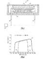
- Figure 1 illustrates a camera 20 having an outer window 22 received in a housing 24 which may be formed of an appropriate metal such as a nickel alloy.
- An image plane 28 and a silicone readout inlet circuit 30, along with a printed wiring board 32 together form a focal plane array of photo-voltaic photo diodes.
- the image plane 28 may be formed of a semiconductor compound including both indium arsenide and gallium arsenide. Cameras that use such image planes may be known as InGaAs cameras.
- a thermal electric cooling sink 34 is positioned to capture heat.
- Input/output pins 90 communicate with a controller 91 which can evaluate and store images captured by camera 20, as known.
- Figure 2 shows a standard bandwidth of capture 40 for a shortwave infrared camera.
- the cameras have typically been designed to capture the entire bandwidth range of about 0.9 - 1.7 microns.
- the camera of Figure 1 is provided with a filter 26 which acts to limit the bandwidth of the shortwave infrared bandwidth which will reach the image plane 28. As shown in this embodiment, the filter 26 is placed directly on the image plane 28.
- the filter 26 may be any interference or dichroic bandwidth filter or any other appropriate filter capable of filtering the bandwidth of shortwave infrared light that reaches the image plane 28.
- the filter 26 may be a simple filter coating applied directly to the surface of the image plane 28 or may be a separate filter which is attached to the plane.
- FIG. 3 shows yet another embodiment wherein a filter 98 is attached directly to the window 96 which may operate much like the window 22 in the camera 20.
- Dichroic filters and how they can be applied to various surfaces are known and within the skill of a worker in this art given the goals of this application as follows.
- the filter may limit the shortwave infrared bandwidth which reaches the image plane 28 such as shown at 42 in Figure 2 .
- a shorter end 44 of the capture bandwidth 42 is approximately 1.1 microns while a longer end 46 is just above about 1.5 microns.
- Figure 4 shows an embodiment 120 wherein there may not be a filter. Rather, the image plane 128 is modified such that it is only sensitive to the bandwidths such as bandwidth 42.
- the long wave cut-off point for a standard photo detector is associated with the ratio of indium arsenide to gallium arsenide.
- a worker of ordinary skill in the art given the teachings of this application would know how to modify that ratio such that the bandwidth 42 is all that is captured and not the entire bandwidth 40.
- This alteration may create a crystal lattice mismatch of an absorbing layer to a substrate which could result in non-uniformities.
- it may be preferred to add phosphide to an absorbing layer making it a compound that alters a bandwidth to a shorter bandwidth while also maintaining a lattice matched to the substrate.
- Aluminum may also be used rather than phosphide.
- a first layer of the detecting structure in the image plane 130 passes light through before hitting a detection layer.
- the first layer can be modified to remove its normal absorbing cut-out from the approximately 0.9 current prior art of the bandwidth 40 closer to the 1.1 micron wavelength. One can do this by increasing the thickness, such that the combination prevents photons short of 1.1 microns from reaching the detecting layer.
- These first layer changes can be combined with the changes mentioned above to a detector bandwidth such that the bandwidth 42 will be achieved.
- Detectors can be designed for front illumination where the light reaches the detection layer through the top surface or back illumination where the light travels through the backside or substrate layer.
- the embodiments mentioned above can be applied either design.
- the camera excludes wavelengths that are shorter than 1.0 microns. In a narrower embodiment, the excluded wavelengths include wavelengths shorter than approximately 1.1 microns. In embodiments, the excluded wavelengths also exclude wavelengths longer than 1.6 microns, and more narrowly wavelengths that are longer than approximately 1.5 microns.
- a filter such as described above can also be manufactured to have one or more notch filters layered together to exclude specific wavelengths. These could be assembled in any of the locations described above.
Landscapes
- Toxicology (AREA)
- Health & Medical Sciences (AREA)
- Physics & Mathematics (AREA)
- Multimedia (AREA)
- Signal Processing (AREA)
- Engineering & Computer Science (AREA)
- General Physics & Mathematics (AREA)
- Optics & Photonics (AREA)
- Photometry And Measurement Of Optical Pulse Characteristics (AREA)
- Transforming Light Signals Into Electric Signals (AREA)
- Blocking Light For Cameras (AREA)
- Camera Bodies And Camera Details Or Accessories (AREA)
- Solid State Image Pick-Up Elements (AREA)
- Studio Devices (AREA)
Abstract
Description
- This application relates to a camera for capturing images in a shortwave infrared bandwidth wherein modifications are made to eliminate capture of certain portions of the shortwave infrared bandwidth.
- Various camera systems are known and utilized for any number of applications. One type of camera has an image detecting device which may be a photo-voltaic photo diode. These cameras are known to capture images in what is known as the shortwave infrared (SWIR) bandwidth. This may also be known in some applications as "near infrared." A capture bandwidth for such cameras may be between about 0.9 and 1.7 microns.
- Such cameras have particularly good application in capturing images in situations where normal visual light images would be compromised. As an example, night vision cameras may operate across this bandwidth. When such cameras are used for night vision systems on commercial land vehicles such as cars, buses and trucks, the full range of such SWIR bandwidth is not needed.
- A camera comprises an image plane for capturing shortwave infrared wavelengths. The image plane captures only a portion of a shortwave infrared wavelength band, and excludes other wavelengths. A method of designing a camera is also disclosed.
- These and other features may be best understood from the following drawings and specification.
-
-
Figure 1 shows an embodiment. -
Figure 2 shows a feature ofFigure 1 embodiment. -
Figure 3 shows another embodiment. -
Figure 4 shows yet another embodiment. -
Figure 1 illustrates acamera 20 having anouter window 22 received in ahousing 24 which may be formed of an appropriate metal such as a nickel alloy. Animage plane 28 and a siliconereadout inlet circuit 30, along with a printedwiring board 32 together form a focal plane array of photo-voltaic photo diodes. In one embodiment, theimage plane 28 may be formed of a semiconductor compound including both indium arsenide and gallium arsenide. Cameras that use such image planes may be known as InGaAs cameras. A thermalelectric cooling sink 34 is positioned to capture heat. Input/output pins 90 communicate with acontroller 91 which can evaluate and store images captured bycamera 20, as known. -
Figure 2 shows a standard bandwidth ofcapture 40 for a shortwave infrared camera. - The cameras have typically been designed to capture the entire bandwidth range of about 0.9 - 1.7 microns.
- The camera of
Figure 1 is provided with afilter 26 which acts to limit the bandwidth of the shortwave infrared bandwidth which will reach theimage plane 28. As shown in this embodiment, thefilter 26 is placed directly on theimage plane 28. - The
filter 26 may be any interference or dichroic bandwidth filter or any other appropriate filter capable of filtering the bandwidth of shortwave infrared light that reaches theimage plane 28. Thefilter 26 may be a simple filter coating applied directly to the surface of theimage plane 28 or may be a separate filter which is attached to the plane. -
Figure 3 shows yet another embodiment wherein afilter 98 is attached directly to thewindow 96 which may operate much like thewindow 22 in thecamera 20. - Dichroic filters and how they can be applied to various surfaces are known and within the skill of a worker in this art given the goals of this application as follows.
- Returning to
Figure 2 , the filter may limit the shortwave infrared bandwidth which reaches theimage plane 28 such as shown at 42 inFigure 2 . Now, ashorter end 44 of the capture bandwidth 42 is approximately 1.1 microns while alonger end 46 is just above about 1.5 microns. - When such cameras are used for night vision systems on commercial land vehicles such as cars, buses and trucks, the full range of the SWIR bandwidth is not needed. Instead, only the range 42 between about 0.9 and 1.5 microns is needed.
-
Figure 4 shows anembodiment 120 wherein there may not be a filter. Rather, theimage plane 128 is modified such that it is only sensitive to the bandwidths such as bandwidth 42. - As an example, it is known that the long wave cut-off point for a standard photo detector is associated with the ratio of indium arsenide to gallium arsenide. A worker of ordinary skill in the art given the teachings of this application would know how to modify that ratio such that the bandwidth 42 is all that is captured and not the
entire bandwidth 40. - This alteration may create a crystal lattice mismatch of an absorbing layer to a substrate which could result in non-uniformities. Thus, it may be preferred to add phosphide to an absorbing layer making it a compound that alters a bandwidth to a shorter bandwidth while also maintaining a lattice matched to the substrate. Aluminum may also be used rather than phosphide.
- A first layer of the detecting structure in the image plane 130 passes light through before hitting a detection layer. The first layer can be modified to remove its normal absorbing cut-out from the approximately 0.9 current prior art of the
bandwidth 40 closer to the 1.1 micron wavelength. One can do this by increasing the thickness, such that the combination prevents photons short of 1.1 microns from reaching the detecting layer. These first layer changes can be combined with the changes mentioned above to a detector bandwidth such that the bandwidth 42 will be achieved. - Detectors can be designed for front illumination where the light reaches the detection layer through the top surface or back illumination where the light travels through the backside or substrate layer. The embodiments mentioned above can be applied either design.
- Finally, returning to
Figure 1 , the modifications to theimage plane 128, as mentioned with regard toFigure 4 , can also be utilized in combination with the filter structure ofFigure 1 . For this reason, anoptical filter 126 is shown inFigure 4 . - The use of both of these features will result in a camera that is unlikely to actually capture a wavelength in the excluded bands between the bandwidth 42 and the
bandwidth 40. - While an example of the excluded wavelengths is illustrated outside of band 42 in
Figure 2 , it should be understood that lesser wavelengths may be excluded, or more could be excluded. In one embodiment, the camera excludes wavelengths that are shorter than 1.0 microns. In a narrower embodiment, the excluded wavelengths include wavelengths shorter than approximately 1.1 microns. In embodiments, the excluded wavelengths also exclude wavelengths longer than 1.6 microns, and more narrowly wavelengths that are longer than approximately 1.5 microns. - A filter such as described above, can also be manufactured to have one or more notch filters layered together to exclude specific wavelengths. These could be assembled in any of the locations described above.
- Although embodiments of this invention have been disclosed, a worker of ordinary skill in this art would recognize that certain modifications would come within the scope of this invention. For that reason, the following claims should be studied to determine the true scope and content of this invention.
Claims (15)
- A camera comprising:an image plane (28) for capturing shortwave infrared wavelengths; andsaid image plane capturing only a portion of a shortwave infrared wavelength band, and excluding other wavelengths.
- The camera as set forth in claim 1, wherein said image plane excludes wavelengths at both a shorter end of the shortwave infrared wavelength band and wavelengths at a longer end of the shortwave infrared wavelength band.
- The camera as set forth in claim 1, wherein said shortwave infrared wavelength is defined beginning at approximately .9 microns and said camera image plane includes wavelengths shorter than about 1.0 microns.
- The camera as set forth in claim 3, wherein said excluded wavelengths include wavelengths shorter than approximately 1.1 micron.
- The camera as set forth in claim 1, wherein said excluded wavelengths exclude wavelengths longer than 1.6 micron.
- The camera as set forth in claim 5, wherein said excluded wavelengths exclude wavelengths greater than approximately 1.5 micron.
- The camera as set forth in claim 1, wherein said camera includes a filter (26) for excluding said excluded wavelengths.
- The camera as set forth in claim 7, wherein said filter (26) is placed directly on said image plane.
- The camera as set forth in claim 7, wherein said filter is a filter coating applied on said image plane.
- The camera as set forth in claim 7, further comprising a housing (24) for said camera including a window (22), and said filter is placed on said window.
- The camera as set forth in claim 9, wherein said image plane is altered such that it only captures images in said portion of said shortwave infrared wavelength band and excludes said excluded wavelengths.
- The camera as set forth in claim 11, wherein said image plane includes a semiconductor compound including indium arsenide and gallium arsenide and a ratio of said indium arsenide to said gallium arsenide is designed to exclude longer ones of said other wavelengths.
- The camera as set forth in claim 11, wherein at least one of a phosphide and aluminum may be adding to an absorbing layer to exclude shorter ones of said other wavelengths.
- The camera as set forth in claim 1, wherein said image plane is altered such that it only captures images in said portion of said shortwave infrared wavelength band and excludes said excluded wavelengths.
- A method of designing a camera including the steps of:a) providing an image plane for capturing shortwave infrared wavelengths; andb) designing said camera such that said image plane captures a portion of a shortwave infrared wavelength band, and excludes other wavelengths, with the exclusion being achieved by providing a filter to filter said excluded other wavelengths, and/or by modifying the image plane such that it only captures said portion of said shortwave infrared wavelength bands.
Applications Claiming Priority (2)
| Application Number | Priority Date | Filing Date | Title |
|---|---|---|---|
| US201361911116P | 2013-12-03 | 2013-12-03 | |
| US14/171,859 US9485439B2 (en) | 2013-12-03 | 2014-02-04 | Shortwave infrared camera with bandwidth restriction |
Publications (1)
| Publication Number | Publication Date |
|---|---|
| EP2882185A1 true EP2882185A1 (en) | 2015-06-10 |
Family
ID=52006849
Family Applications (1)
| Application Number | Title | Priority Date | Filing Date |
|---|---|---|---|
| EP14194938.8A Ceased EP2882185A1 (en) | 2013-12-03 | 2014-11-26 | Shortwave infrared camera with bandwidth restriction |
Country Status (4)
| Country | Link |
|---|---|
| US (1) | US9485439B2 (en) |
| EP (1) | EP2882185A1 (en) |
| JP (1) | JP6437283B2 (en) |
| KR (1) | KR102220277B1 (en) |
Cited By (1)
| Publication number | Priority date | Publication date | Assignee | Title |
|---|---|---|---|---|
| EP3166151A1 (en) * | 2015-10-26 | 2017-05-10 | Sensors Unlimited, Inc. | Quantum efficiency restricted infrared focal plane arrays |
Families Citing this family (1)
| Publication number | Priority date | Publication date | Assignee | Title |
|---|---|---|---|---|
| KR102209218B1 (en) * | 2017-11-15 | 2021-01-29 | (주)토핀스 | Short Wave Infrared Camera Optical System for The Long Range Image Monitoring |
Citations (3)
| Publication number | Priority date | Publication date | Assignee | Title |
|---|---|---|---|---|
| WO2000054217A2 (en) * | 1999-03-05 | 2000-09-14 | Flir Systems, Inc. | Enhanced vision system sensitive to infrared radiation |
| US20070278406A1 (en) * | 2004-01-10 | 2007-12-06 | Karsten Haug | Night-Vision System For Motor Vehicles Having A Partial Optical Filter |
| WO2012143927A1 (en) * | 2011-04-17 | 2012-10-26 | Elta Systems Ltd. | Night vision system and method |
Family Cites Families (19)
| Publication number | Priority date | Publication date | Assignee | Title |
|---|---|---|---|---|
| US20060055800A1 (en) * | 2002-12-18 | 2006-03-16 | Noble Device Technologies Corp. | Adaptive solid state image sensor |
| US7274393B2 (en) | 2003-02-28 | 2007-09-25 | Intel Corporation | Four-color mosaic pattern for depth and image capture |
| US20050002028A1 (en) * | 2003-07-02 | 2005-01-06 | Steven Kasapi | Time resolved emission spectral analysis system |
| US7821552B2 (en) | 2005-12-27 | 2010-10-26 | Sanyo Electric Co., Ltd. | Imaging apparatus provided with imaging device having sensitivity in visible and infrared regions |
| JP2007201432A (en) * | 2005-12-28 | 2007-08-09 | Sumitomo Electric Ind Ltd | Imaging device, visual field support device, night vision device, navigation support device, and monitoring device |
| JP2007264116A (en) * | 2006-03-27 | 2007-10-11 | Mitsumi Electric Co Ltd | Camera module for infrared sensor |
| JP2007311447A (en) | 2006-05-17 | 2007-11-29 | Sanyo Electric Co Ltd | Photoelectric conversion device |
| JP4396684B2 (en) | 2006-10-04 | 2010-01-13 | ソニー株式会社 | Method for manufacturing solid-state imaging device |
| JP4386096B2 (en) | 2007-05-18 | 2009-12-16 | ソニー株式会社 | Image input processing apparatus and method |
| JP2009212824A (en) * | 2008-03-04 | 2009-09-17 | Funai Electric Co Ltd | Skin area detection imaging apparatus |
| US20100022678A1 (en) * | 2008-07-24 | 2010-01-28 | Zimmer, Inc. | Reduction of free radicals in crosslinked polyethylene by infrared heating |
| WO2010052593A1 (en) | 2008-11-04 | 2010-05-14 | Ecole Polytechnique Federale De Lausanne (Epfl) | Camera design for the simultaneous capture of near-infrared and visible images |
| JP2011151596A (en) * | 2010-01-21 | 2011-08-04 | Rohm Co Ltd | Biometrics authentication device and mobile device |
| JP2011199798A (en) * | 2010-03-24 | 2011-10-06 | Sony Corp | Physical information obtaining apparatus, solid-state imaging apparatus, and physical information obtaining method |
| JP5009395B2 (en) * | 2010-05-26 | 2012-08-22 | 日立マクセル株式会社 | Imaging device |
| CN102377937B (en) * | 2010-08-04 | 2015-07-15 | 株式会社日立国际电气 | Shooting device |
| US8558890B2 (en) | 2010-08-12 | 2013-10-15 | Goodrich Corporation | Aerial reconnaissance camera system with atmospheric dispersion correction |
| US8811664B2 (en) * | 2011-12-06 | 2014-08-19 | Xerox Corporation | Vehicle occupancy detection via single band infrared imaging |
| KR20150118591A (en) * | 2012-03-30 | 2015-10-23 | 삼성전기주식회사 | Camera module |
-
2014
- 2014-02-04 US US14/171,859 patent/US9485439B2/en active Active
- 2014-11-19 JP JP2014234103A patent/JP6437283B2/en active Active
- 2014-11-26 EP EP14194938.8A patent/EP2882185A1/en not_active Ceased
- 2014-11-28 KR KR1020140167977A patent/KR102220277B1/en active Active
Patent Citations (3)
| Publication number | Priority date | Publication date | Assignee | Title |
|---|---|---|---|---|
| WO2000054217A2 (en) * | 1999-03-05 | 2000-09-14 | Flir Systems, Inc. | Enhanced vision system sensitive to infrared radiation |
| US20070278406A1 (en) * | 2004-01-10 | 2007-12-06 | Karsten Haug | Night-Vision System For Motor Vehicles Having A Partial Optical Filter |
| WO2012143927A1 (en) * | 2011-04-17 | 2012-10-26 | Elta Systems Ltd. | Night vision system and method |
Cited By (2)
| Publication number | Priority date | Publication date | Assignee | Title |
|---|---|---|---|---|
| EP3166151A1 (en) * | 2015-10-26 | 2017-05-10 | Sensors Unlimited, Inc. | Quantum efficiency restricted infrared focal plane arrays |
| US9842868B2 (en) | 2015-10-26 | 2017-12-12 | Sensors Unlimited, Inc. | Quantum efficiency (QE) restricted infrared focal plane arrays |
Also Published As
| Publication number | Publication date |
|---|---|
| US20150156426A1 (en) | 2015-06-04 |
| KR20150064674A (en) | 2015-06-11 |
| KR102220277B1 (en) | 2021-02-24 |
| JP2015109441A (en) | 2015-06-11 |
| JP6437283B2 (en) | 2018-12-12 |
| US9485439B2 (en) | 2016-11-01 |
Similar Documents
| Publication | Publication Date | Title |
|---|---|---|
| US20230154179A1 (en) | System and method for space object detection in daytime sky images | |
| CN110035238B (en) | Compact infrared camera for automotive safety and driving systems | |
| CN203589032U (en) | Image-capturing element and image-capturing device | |
| EP3133646A2 (en) | Sensor assembly with selective infrared filter array | |
| US10578739B2 (en) | Optoelectronic modules for the acquisition of spectral and distance data | |
| JP6388669B2 (en) | Solid-state imaging device | |
| US20160309098A1 (en) | Image capturing device with an image sensor and a thermal infrared sensor as well as motor vehicle with an image capturing device | |
| US20140285420A1 (en) | Imaging device, displaying device, mobile terminal device, and camera module | |
| CN108474887A (en) | Heat-insulated optical filter and monitoring system | |
| US20180328694A1 (en) | Thermal reflex sight | |
| US9485439B2 (en) | Shortwave infrared camera with bandwidth restriction | |
| CN106851078A (en) | A kind of filtering apparatus and camera module | |
| US9110292B1 (en) | Multiple filter photon conversion assembly | |
| US9798054B1 (en) | Camera assembly for use on a vehicle | |
| EP3166151B1 (en) | Quantum efficiency restricted infrared focal plane arrays | |
| KR20200078480A (en) | Solid state imaging element, manufacturing method and electronic device | |
| EP3350986B1 (en) | Systems and methods for detecting light sources | |
| CN110235252A (en) | Apparatus for improved multispectral detection | |
| KR20220002244A (en) | Pixels for Semiconductor Image Sensors and Methods for Manufacturing Pixels | |
| EP2639778A1 (en) | Method and device for detection of multiple flame types | |
| US10845674B2 (en) | Ghost reducing device, imaging device including same, ghost reducing method, and imaging optical system | |
| US12148777B2 (en) | Image sensor with spectral-filter-based crosstalk suppression | |
| US10171758B2 (en) | Multi-spectrum imaging | |
| FR2968777A1 (en) | System for acquiring image during conditions e.g. fog, with low level of light, for helmet display system used by pilot of aircraft, has merging unit for merging images from visible and short wave infrared sensors to generate final image | |
| JP5184244B2 (en) | Imaging device |
Legal Events
| Date | Code | Title | Description |
|---|---|---|---|
| PUAI | Public reference made under article 153(3) epc to a published international application that has entered the european phase |
Free format text: ORIGINAL CODE: 0009012 |
|
| 17P | Request for examination filed |
Effective date: 20141126 |
|
| AK | Designated contracting states |
Kind code of ref document: A1 Designated state(s): AL AT BE BG CH CY CZ DE DK EE ES FI FR GB GR HR HU IE IS IT LI LT LU LV MC MK MT NL NO PL PT RO RS SE SI SK SM TR |
|
| AX | Request for extension of the european patent |
Extension state: BA ME |
|
| R17P | Request for examination filed (corrected) |
Effective date: 20151209 |
|
| RBV | Designated contracting states (corrected) |
Designated state(s): AL AT BE BG CH CY CZ DE DK EE ES FI FR GB GR HR HU IE IS IT LI LT LU LV MC MK MT NL NO PL PT RO RS SE SI SK SM TR |
|
| 17Q | First examination report despatched |
Effective date: 20160329 |
|
| 18R | Application refused |
Effective date: 20171103 |