EP2882108A1 - Power supply for transmission arrangement - Google Patents
Power supply for transmission arrangement Download PDFInfo
- Publication number
- EP2882108A1 EP2882108A1 EP13306670.4A EP13306670A EP2882108A1 EP 2882108 A1 EP2882108 A1 EP 2882108A1 EP 13306670 A EP13306670 A EP 13306670A EP 2882108 A1 EP2882108 A1 EP 2882108A1
- Authority
- EP
- European Patent Office
- Prior art keywords
- dmt
- data
- transmission arrangement
- transceiver
- pwm signal
- Prior art date
- Legal status (The legal status is an assumption and is not a legal conclusion. Google has not performed a legal analysis and makes no representation as to the accuracy of the status listed.)
- Granted
Links
- 230000005540 biological transmission Effects 0.000 title claims abstract description 39
- IYZMXHQDXZKNCY-UHFFFAOYSA-N 1-n,1-n-diphenyl-4-n,4-n-bis[4-(n-phenylanilino)phenyl]benzene-1,4-diamine Chemical compound C1=CC=CC=C1N(C=1C=CC(=CC=1)N(C=1C=CC(=CC=1)N(C=1C=CC=CC=1)C=1C=CC=CC=1)C=1C=CC(=CC=1)N(C=1C=CC=CC=1)C=1C=CC=CC=1)C1=CC=CC=C1 IYZMXHQDXZKNCY-UHFFFAOYSA-N 0.000 claims abstract description 13
- 230000008878 coupling Effects 0.000 claims abstract description 11
- 238000010168 coupling process Methods 0.000 claims abstract description 11
- 238000005859 coupling reaction Methods 0.000 claims abstract description 11
- 125000004122 cyclic group Chemical group 0.000 claims abstract description 7
- 230000003071 parasitic effect Effects 0.000 claims description 2
- 239000003990 capacitor Substances 0.000 description 8
- 238000004891 communication Methods 0.000 description 7
- 239000000969 carrier Substances 0.000 description 5
- 238000007599 discharging Methods 0.000 description 5
- 238000011144 upstream manufacturing Methods 0.000 description 4
- 230000008859 change Effects 0.000 description 3
- 230000001419 dependent effect Effects 0.000 description 3
- 238000006243 chemical reaction Methods 0.000 description 2
- 238000012937 correction Methods 0.000 description 2
- 238000001514 detection method Methods 0.000 description 2
- 230000006870 function Effects 0.000 description 2
- 238000011068 loading method Methods 0.000 description 2
- 230000007246 mechanism Effects 0.000 description 2
- 230000001105 regulatory effect Effects 0.000 description 2
- 230000004044 response Effects 0.000 description 2
- 238000005070 sampling Methods 0.000 description 2
- 238000012546 transfer Methods 0.000 description 2
- SYUPLLHVMCLXEM-UHFFFAOYSA-N 4,5-dichloro-2-(3-methylphenyl)pyridazin-3-one Chemical compound CC1=CC=CC(N2C(C(Cl)=C(Cl)C=N2)=O)=C1 SYUPLLHVMCLXEM-UHFFFAOYSA-N 0.000 description 1
- RYGMFSIKBFXOCR-UHFFFAOYSA-N Copper Chemical compound [Cu] RYGMFSIKBFXOCR-UHFFFAOYSA-N 0.000 description 1
- 230000005526 G1 to G0 transition Effects 0.000 description 1
- 230000006978 adaptation Effects 0.000 description 1
- 230000001276 controlling effect Effects 0.000 description 1
- 229910052802 copper Inorganic materials 0.000 description 1
- 239000010949 copper Substances 0.000 description 1
- 230000003247 decreasing effect Effects 0.000 description 1
- 238000013461 design Methods 0.000 description 1
- 238000003745 diagnosis Methods 0.000 description 1
- 230000000694 effects Effects 0.000 description 1
- 239000000835 fiber Substances 0.000 description 1
- 238000009432 framing Methods 0.000 description 1
- 238000009499 grossing Methods 0.000 description 1
- 238000003780 insertion Methods 0.000 description 1
- 230000037431 insertion Effects 0.000 description 1
- 238000002955 isolation Methods 0.000 description 1
- 238000013507 mapping Methods 0.000 description 1
- 238000000034 method Methods 0.000 description 1
- 230000000737 periodic effect Effects 0.000 description 1
- 230000008569 process Effects 0.000 description 1
- 229920006395 saturated elastomer Polymers 0.000 description 1
- 238000007493 shaping process Methods 0.000 description 1
- 230000003595 spectral effect Effects 0.000 description 1
- 230000007704 transition Effects 0.000 description 1
- 238000013519 translation Methods 0.000 description 1
Images

Classifications
-
- H—ELECTRICITY
- H04—ELECTRIC COMMUNICATION TECHNIQUE
- H04B—TRANSMISSION
- H04B3/00—Line transmission systems
- H04B3/02—Details
- H04B3/32—Reducing cross-talk, e.g. by compensating
-
- H—ELECTRICITY
- H02—GENERATION; CONVERSION OR DISTRIBUTION OF ELECTRIC POWER
- H02M—APPARATUS FOR CONVERSION BETWEEN AC AND AC, BETWEEN AC AND DC, OR BETWEEN DC AND DC, AND FOR USE WITH MAINS OR SIMILAR POWER SUPPLY SYSTEMS; CONVERSION OF DC OR AC INPUT POWER INTO SURGE OUTPUT POWER; CONTROL OR REGULATION THEREOF
- H02M3/00—Conversion of DC power input into DC power output
- H02M3/02—Conversion of DC power input into DC power output without intermediate conversion into AC
- H02M3/04—Conversion of DC power input into DC power output without intermediate conversion into AC by static converters
- H02M3/10—Conversion of DC power input into DC power output without intermediate conversion into AC by static converters using discharge tubes with control electrode or semiconductor devices with control electrode
- H02M3/145—Conversion of DC power input into DC power output without intermediate conversion into AC by static converters using discharge tubes with control electrode or semiconductor devices with control electrode using devices of a triode or transistor type requiring continuous application of a control signal
- H02M3/155—Conversion of DC power input into DC power output without intermediate conversion into AC by static converters using discharge tubes with control electrode or semiconductor devices with control electrode using devices of a triode or transistor type requiring continuous application of a control signal using semiconductor devices only
- H02M3/156—Conversion of DC power input into DC power output without intermediate conversion into AC by static converters using discharge tubes with control electrode or semiconductor devices with control electrode using devices of a triode or transistor type requiring continuous application of a control signal using semiconductor devices only with automatic control of output voltage or current, e.g. switching regulators
Definitions
- the present invention relates to power supplies for use in transmission arrangements configured to transmit and/or receive cyclically extended data symbols, such as Discrete Multi-Tone (DMT) transceivers.
- DMT Discrete Multi-Tone
- a linear regulator provides the desired output voltage by dissipating excess power in ohmic losses in the form of heat, e.g. in a resistor or in the collector-emitter region of a pass transistor in its active mode. Hence, its maximum power efficiency is voltage-out/voltage-in dependent since the voltage difference is wasted.
- an SMPS regulates either output voltage or current by switching ideal storage elements, like inductors or capacitors.
- the switching elements e.g., a MOSFET transistor operated in blocked or saturated state
- the switching elements has a very low saturation voltage and a low resistance when closed, and carry no current when open, and so the converters can theoretically operate with 100% efficiency (i.e., all input power is delivered to the load; no power is wasted as dissipated heat).
- an SMPS typically includes a MOSFET switch T, a diode D, an output capacitor C and an inductor L coupled as per fig. 1 .
- the SMPS is fed with an input voltage source V IN and produces a regulated voltage V OUT for feeding a load Z L .
- This SMPS topology is referred to as Step-Up (or Boost).
- Other SMPS topologies can alternatively be used, such as step-down (or Buck), or step-up/down (or buck/boost).
- the MOSFET T is switched ON and the inductor L is connected to the input voltage source V IN .
- the inductor's current I L follows a linear ramp with positive slope V IN /L as per equation (2).
- the diode D is reverse-biased and thus isolates the output capacitor C from the inductor L and the input voltage source V IN .
- the output capacitor C supports the load Z L while energy builds up in the inductor L as per equation (1).
- the MOSFET T is switched OFF, thereby disrupting the increasing current I L and creating an electro-magnetic force (emf) that tends to sustain the inductor's current.
- emf electro-magnetic force
- This emf adds as an additional voltage to the voltage source V IN , and forward-bias the diode D so as the inductor's current can now recharge the output capacitor C and sustain the current drain from the load Z L .
- V IN -V OUT -V BIAS is applied across the inductor L, V BIAS denoting the forward-bias voltage of the diode D, and the inductor's current I L follows a linear ramp with negative slope (V IN -V OUT -V BIAS )/L as per equation (2).
- the frequency fc 1/Tc of the PWM signal that controls the operation of the SMPS shall be high enough so as smaller size and lighter weight coils can advantageously be used, and low enough so as switching losses remain small.
- fc is about a few hundreds kHz.
- the PWM signal is typically locked on a frequency that is a multiple of the tone spacing, e.g. 4,3125kHZ or 8,625kHz for DSL transmissions.
- the FFT window length has an integer number of PWM cycles, meaning that distortion only happens at bins with a frequency that is a multiple of the frequency fc, and has zero crossing at all other bins.
- the affected tones don't change. If a free-running clock was used instead, then various tones would get affected on account of the load or temperature fluctuations. This may ultimately leads to bit errors as the bit swap and Seamless Rate Adaptation (SRA) mechanisms are not fast enough to track these noise variations and the error correction mechanisms may have insufficient capability.
- SRA Seamless Rate Adaptation
- a transmission arrangement comprises a switched-mode power supply controlled by a PWM signal comprising successive cycles, a transceiver for transmitting or receiving successive cyclically-extended data symbols with a common symbol period T DMT , the cyclically-extended data symbols respectively including a data part with a common data period T DATA and a cyclic extension of the data part, and a coupling path between the switched-mode power supply and the transceiver.
- the PWM signal is configured such that successive periods of the PWM signal comprising an integer number P of cycles respectively span an integer number M of symbol periods T DMT .
- the successively transmitted or received cyclically-extended data symbols are grouped into time frames spanning an integer number L of symbol periods T DMT , and M is equal to L.
- f DMT 1/T DMT is equal to 4 kHz or 8 kHz
- ⁇ f 1/T DATA is equal to 4,3125 kHz or 8,625 kHz respectively.
- the coupling path is a parasitic coupling path whereby the switched-mode power supply generates electromagnetic interference that affect the operation of the transceiver.
- Such a transmission arrangement may form part of an access node that supports wired communication with subscriber devices over an access plant, such as a Digital Subscriber Line Access Multiplexer (DSLAM), an Ethernet switch, an edge router, etc, and deployed at a Central Office (CO) or as a fiber-fed remote unit closer to subscriber premises (street cabinet, pole cabinet, building cabinet, etc).
- DSLAM Digital Subscriber Line Access Multiplexer
- CO Central Office
- fiber-fed remote unit closer to subscriber premises street cabinet, pole cabinet, building cabinet, etc.
- the idea is to lock the frequency of the PWM signal that is used to control the SMPS to a multiple of the symbol rate so as to make the converter noise stationary.
- This stationary noise can be considered as an offset signal that can be easily subtracted in the frequency or time domain at the transmit or receive side.
- the frequency equalizer could also center the receive constellation points on a square grid so as to remove (or at least mitigate) this stationary offset.
- the PWM signal has a frequency that is a common multiple of both the symbol rate and the carrier spacing, for instance the Least Common Multiplier (LCM) of these both values, provided such a common multiple value is within the operational frequency range dictated by the SMPS design and components.
- LCM Least Common Multiplier
- the symbols may be grouped into time frames comprising an integer number of DMT symbols. If so, we may alternatively lock the PWM signal to a multiple of the frame rate. In this case, a more complex algorithm is required to predict the shape of the converter noise in each DMT symbol depending on the relative position of the DMT symbol in the frame.
- the DSP 41 is configured to operate downstream and upstream communication channels for conveying user traffic over a transmission medium.
- the transmission medium can be of any type, including one or more Unshielded Twisted Pairs (UTP), a co-axial cable, a power line, etc.
- UTP Unshielded Twisted Pairs
- two SMPSs 30 and one transceiver 40 have been plotted in fig. 2 as forming part of the transmission arrangement 1.
- a first SMPS 30 1 supplies a positive supply voltage value V CC1 for feeding the DSP 41 via a power supply path 60 1 ; and a second SMPS 30 2 supplies opposite supply voltage values ⁇ V CC2 for feeding the AFE 42 via two respective power supply paths 60 2 and 60 3 .
- the SMPSs 30 individually comprise:
- the controller 32 adjusts the duty cycle D of the PWM signal by sensing the voltage value observed at the output of the SMPS 30. If the output voltage value is too low, then the duty cycle D is increased so as to allow more energy to be stored in the storage element of the voltage converter 31 and released into the load. The way around, if the output voltage value is too high, then the duty cycle D is decreased.
- the operations of the SMPSs 30 cause some unwanted distortions in the transmit and/or receive path of the transceiver 40. These distortions mostly consists of small ripples with frequency fc that superimpose over the transmit or receive signal, e.g. on account of the PSRR of the line driver or LNA of the AFE 42.
- the frequency fc of the PWM signal S PWM is configured to be equal to a common multiple of both the DMT symbol rate F DMT and the carrier spacing ⁇ f, or equivalently the symbol period T DMT and the data period T DATA spans an integer number of PWM cycles Tc.
- the controller 32 may switch between different frequency values during successive cycles of the PWM signal S PWM so as to approximate the desired value. If such a choice is made, the symbol period T DMT and the data period T DATA would still spans an integer number of PWM cycles (with respective durations).
- the noise signal generated by the SMPSs 30 that superimposes on the useful transmit or receive signal becomes stationary, and thus can be easily compensated at the transmit or receive side.
- the receiver can subtract an estimate of this noise signal with almost stationary phase and amplitude, which corresponds to a linear translation of the constellation grid that is used for demodulating the receive frequency samples.
- This constellation shift is expected to be frequency dependent, and can take place before or after frequency equalization depending on whether the SMPS noise is predominant at transmit or receive side.
- the frequency fc of the PWM signal S PWM is configured to be a multiple of the DMT symbol rate F DMT only, or equivalently the symbol period T DMT spans an integer number of PWM cycles Tc. This would be the case if for instance the common multiple value is outside the operational frequency range of the SMPSs 30.
- the DMT symbols are grouped into TDD frames.
- One TDD frame spans an integer number M of DMT symbols (including any necessary guard periods for transitioning between transmit and receive operation).
- the frequency fc of the PWM signal S PWM can be configured to be a multiple of the frame rate f FRAME , or equivalently the frame periods T FRAME spans an integer number of PWM cycles Tc.
- the noise induced by the SMPS 30 is no longer stationary for the successive DMT symbols, yet remains stationary if only symbols with a given relative position within the TDD frame are considered. This implies that the applied constellation shift further depends on the relative position within the TDD frame of the DMT symbol that is considered.
Landscapes
- Engineering & Computer Science (AREA)
- Computer Networks & Wireless Communication (AREA)
- Signal Processing (AREA)
- Cable Transmission Systems, Equalization Of Radio And Reduction Of Echo (AREA)
Abstract
Description
- The present invention relates to power supplies for use in transmission arrangements configured to transmit and/or receive cyclically extended data symbols, such as Discrete Multi-Tone (DMT) transceivers.
- Considering the multiple DC voltage levels required by many electronic devices, designers need a way to convert standard power-source potentials into the voltages dictated by the load. Voltage conversion must be a versatile, efficient, reliable process. Switch-Mode Power Supplies (SMPS) are frequently used to provide the various levels of DC output power needed for modern applications, and are indispensable in achieving highly efficient, reliable DC-DC power-conversion.
- A linear regulator provides the desired output voltage by dissipating excess power in ohmic losses in the form of heat, e.g. in a resistor or in the collector-emitter region of a pass transistor in its active mode. Hence, its maximum power efficiency is voltage-out/voltage-in dependent since the voltage difference is wasted.
- In contrast, an SMPS regulates either output voltage or current by switching ideal storage elements, like inductors or capacitors. The switching elements (e.g., a MOSFET transistor operated in blocked or saturated state) has a very low saturation voltage and a low resistance when closed, and carry no current when open, and so the converters can theoretically operate with 100% efficiency (i.e., all input power is delivered to the load; no power is wasted as dissipated heat).
- Typically, an SMPS includes a MOSFET switch T, a diode D, an output capacitor C and an inductor L coupled as per
fig. 1 . The SMPS is fed with an input voltage source VIN and produces a regulated voltage VOUT for feeding a load ZL. This SMPS topology is referred to as Step-Up (or Boost). Other SMPS topologies can alternatively be used, such as step-down (or Buck), or step-up/down (or buck/boost). - The MOSFET T, which is the actively controlled component in the circuit, is interfaced to a controller CTRL. The controller CTRL applies a Pulse-Width Modulated (PWM) square-wave signal SPWM to the MOSFET's gate, thereby switching the device ON and OFF (see SPWM plot versus time in
fig. 1 ). To maintain a constant output voltage, the controller senses the SMPS output voltage VOUT and varies the duty cycle D of the PWM signal SPWM, dictating how long the MOSFET is ON during each switching period. The value of D, which is the ratio of the square wave's ON time to the switching period Tc, directly affects the voltage VOUT observed at the SMPS output. - The ON and OFF states of the MOSFET T divide the SMPS circuit into two phases: a charging phase and a discharging phase. Energy stored in the inductor L during the charging phase is transferred to the output load ZL and capacitor C during the discharging phase. The capacitor C supports the load and sustains the output voltage VOUT while the inductor L is charging. This cyclical transfer of energy between the circuit elements maintains the output voltage VOUT at the proper value VTARGET, in accordance with the SMPS topology. The inductor L is central to the energy transfer from the source to the load during each switching cycle. It can be advantageously replaced by a transformer so as to DC-isolate the input power source VIN from the load ZL.
- The energy E stored in an inductor L is dependent upon its current IL:
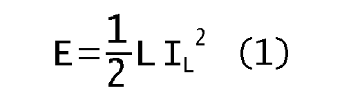
- Therefore, the energy change in the inductor is gauged by the change in its current ΔIL, which is due to the voltage VL applied across the inductor L over a specific time period ΔT:

- During the charging phase, the MOSFET T is switched ON and the inductor L is connected to the input voltage source VIN. As a constant voltage is applied across the inductor L, the inductor's current IL follows a linear ramp with positive slope VIN/L as per equation (2). The diode D is reverse-biased and thus isolates the output capacitor C from the inductor L and the input voltage source VIN. The output capacitor C supports the load ZL while energy builds up in the inductor L as per equation (1).
- During the discharging phase, the MOSFET T is switched OFF, thereby disrupting the increasing current IL and creating an electro-magnetic force (emf) that tends to sustain the inductor's current. This emf adds as an additional voltage to the voltage source VIN, and forward-bias the diode D so as the inductor's current can now recharge the output capacitor C and sustain the current drain from the load ZL. During the discharging phase, the voltage VIN-VOUT-VBIAS is applied across the inductor L, VBIAS denoting the forward-bias voltage of the diode D, and the inductor's current IL follows a linear ramp with negative slope (VIN-VOUT-VBIAS)/L as per equation (2).
- The frequency fc = 1/Tc of the PWM signal that controls the operation of the SMPS shall be high enough so as smaller size and lighter weight coils can advantageously be used, and low enough so as switching losses remain small. Typically, fc is about a few hundreds kHz.
- Some ripples with period Tc will thus superimpose over the almost desired output voltage VTARGET on account of the recharging/discharging cycles (see VOUT plot versus time in
fig. 1 ). When an SMPS is used to feed a transmission arrangement, the ripples on the power supply voltage may cause some unwanted signal distortion on account of interalia the finite Power Supply Rejection ratio (PSRR) of the transmit or receive amplifier. - In order to mitigate the SMPS noise for DMT transceivers, the PWM signal is typically locked on a frequency that is a multiple of the tone spacing, e.g. 4,3125kHZ or 8,625kHz for DSL transmissions. In this way, the FFT window length has an integer number of PWM cycles, meaning that distortion only happens at bins with a frequency that is a multiple of the frequency fc, and has zero crossing at all other bins. Also the affected tones don't change. If a free-running clock was used instead, then various tones would get affected on account of the load or temperature fluctuations. This may ultimately leads to bit errors as the bit swap and Seamless Rate Adaptation (SRA) mechanisms are not fast enough to track these noise variations and the error correction mechanisms may have insufficient capability.
- It is an object of the present invention to further mitigate the interference caused by an SMPS in a transmission arrangement configured to transmit and/or receive cyclically extended data symbols.
- In accordance with a first aspect of the invention, a transmission arrangement comprises a switched-mode power supply controlled by a PWM signal comprising successive cycles, a transceiver for transmitting or receiving successive cyclically-extended data symbols with a common symbol period TDMT, the cyclically-extended data symbols respectively including a data part with a common data period TDATA and a cyclic extension of the data part, and a coupling path between the switched-mode power supply and the transceiver. The PWM signal is configured such that successive periods of the PWM signal comprising an integer number P of cycles respectively span an integer number M of symbol periods TDMT.
- In one embodiment of the invention, the successively transmitted or received cyclically-extended data symbols are grouped into time frames spanning an integer number L of symbol periods TDMT, and M is equal to L.
- In one embodiment of the invention, M is equal to 1.
- In one embodiment of the invention, the PWM signal is further configured such that further successive periods of the PWM signal comprising an integer number K of cycles respectively span one data period TDATA.
- For DSL transceivers, fDMT = 1/TDMT is equal to 4 kHz or 8 kHz, and Δf = 1/TDATA is equal to 4,3125 kHz or 8,625 kHz respectively. If so, P = m · 69 and K = m · 64, m being a non-null positive integer number, meaning that fc = 1/Tc is equal to 276 kHz and 552 kHz respectively, or a multiple thereof.
- In one embodiment of the invention, the coupling path is a power supply path whereby the switched-mode power supply supplies power to an analog circuit of the transceiver, such as a transmit or receive amplifier.
- In one embodiment of the invention, the coupling path is a parasitic coupling path whereby the switched-mode power supply generates electromagnetic interference that affect the operation of the transceiver.
- Such a transmission arrangement may form part of an access node that supports wired communication with subscriber devices over an access plant, such as a Digital Subscriber Line Access Multiplexer (DSLAM), an Ethernet switch, an edge router, etc, and deployed at a Central Office (CO) or as a fiber-fed remote unit closer to subscriber premises (street cabinet, pole cabinet, building cabinet, etc).
- Such a transmission arrangement may alternatively form part of a subscriber device, such as a Digital Subscriber Line (DSL) gateway, a subscriber terminal, etc.
- The idea is to lock the frequency of the PWM signal that is used to control the SMPS to a multiple of the symbol rate so as to make the converter noise stationary. This stationary noise can be considered as an offset signal that can be easily subtracted in the frequency or time domain at the transmit or receive side. For instance, in addition to rotating and scaling the incoming tones, the frequency equalizer could also center the receive constellation points on a square grid so as to remove (or at least mitigate) this stationary offset.
- The frequency of the PWM signal may further be locked to a multiple of the carrier spacing clock Δf = 1/TDATA so as to affect a reduced number of carriers as aforementioned. In this case, the PWM signal has a frequency that is a common multiple of both the symbol rate and the carrier spacing, for instance the Least Common Multiplier (LCM) of these both values, provided such a common multiple value is within the operational frequency range dictated by the SMPS design and components.
- Also, the symbols may be grouped into time frames comprising an integer number of DMT symbols. If so, we may alternatively lock the PWM signal to a multiple of the frame rate. In this case, a more complex algorithm is required to predict the shape of the converter noise in each DMT symbol depending on the relative position of the DMT symbol in the frame.
- The above and other objects and features of the invention will become more apparent and the invention itself will be best understood by referring to the following description of an embodiment taken in conjunction with the accompanying drawings wherein:
-
fig. 1 represents a prior art SMPS whose operation has been previously described; -
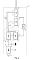
fig. 2 represents a transmission arrangement as per the present invention; and -
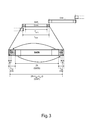
fig. 3 represents cyclic extension of DMT symbols and respective timing information. - There is seen in
fig. 2 atransmission arrangement 1 comprising: -
input terminals 10 to be coupled to an AC voltage source; - a
rectifier 20 for rectifying the AC input signal, coupled to a capacitor C for smoothing the rectified signal into an almost constant voltage value VIN; - one or more SMPSs 30 for converting the input voltage value VIN into respective voltages values VOUT as dictated by the power supply requirements of the respective hardware components of the
transmission arrangement 1; - one or
more transceivers 40 respectively comprising a Digital Signal Processor (DSP) 41 and an Analog Front End (AFE) 42; and - a
clock generation unit 50. - The
DSP 41 is configured to operate downstream and upstream communication channels for conveying user traffic over a transmission medium. The transmission medium can be of any type, including one or more Unshielded Twisted Pairs (UTP), a co-axial cable, a power line, etc. - The
DSP 41 is further configured to operate downstream and upstream control channels that are used to transport control traffic between transceivers, such as diagnosis, management or control commands and responses. Control traffic is multiplexed with user traffic over the transmission medium. - More specifically, the
DSP 41 is for encoding and modulating user and control data into digital DMT symbols, and for de-modulating and decoding user and control data from digital DMT symbols. - The following transmit steps are typically performed within the DSP 41:
- data encoding, such as data multiplexing, framing, scrambling, error control encoding, and data interleaving;
- signal modulation, comprising the steps of ordering the carriers according to a carrier ordering table, parsing the encoded bit stream according to the respective bit loadings of the ordered carriers, and mapping each chunk of bits onto an appropriate transmit constellation point (with respective carrier amplitude and phase), possibly using Trellis Coded Modulation (TCM);
- signal scaling;
- Inverse Fast Fourier Transform (IFFT);
- Cyclic Extension (CE) insertion; and possibly
- time-windowing.
- The following receive steps are typically performed within the DSP 41:
- CE removal, and possibly time-windowing;
- Fast Fourier Transform (FFT);
- frequency equalization;
- signal de-modulation and detection, comprising the steps of applying to each and every equalized frequency sample an appropriate constellation grid, the pattern of which depends on the respective carrier bit loading, detecting the expected transmit constellation point and the corresponding transmit bit sequence, possibly with TCM decoding, and re-ordering all the detected chunks of bits according to the carrier ordering table; and
- data decoding, such as data de-interleaving, error detection and/or correction, de-scrambling, frame delineation and demultiplexing.
- The AFE 42 comprises a Digital-to-Analog Converter (DAC) and an Analog-to-Digital Converter (ADC), a transmit filter and a receive filter for confining the signal energy within the appropriate communication frequency bands while rejecting out-of-band interference, a line driver for amplifying the transmit signal and for driving the transmission medium, and a Low Noise Amplifier (LNA) for amplifying the receive signal with as little noise as possible.
- In case of Frequency Division Duplexing (FDD) operation where downstream and upstream communications operate simultaneously over the same transmission medium in distinct and non-overlapping frequency bands, the AFE 42 further comprises a hybrid for coupling the transmitter output to the transmission medium and the transmission medium to the receiver input while achieving low transmitter-receiver coupling ratio.
- In case of Time Duplexing Division (TDD) operation where downstream and upstream communications operate over the same frequency band but in distinct and non-overlapping time slots, the hybrid can be advantageously omitted as the transmitter and receiver operate in alternate mode: the receive circuitry is switched OFF (or the receive signal is discarded) while the transmit circuitry is active, and the way around, the transmit circuitry is switched OFF while the receive circuitry is active.
- The AFE 42 further comprises impedance-matching circuitry for adapting to the characteristic impedance of the transmission medium, clipping circuitry for clipping any voltage or current surge occurring over the transmission medium, and isolation circuitry (typically a transformer) for DC-isolating the transceiver from the transmission medium.
- The clock generation unit (CLK) 50 supplies a reference clock signal SCLK with stable frequency fCLK = 1/TCLK to the
SMPSs 30 and to thetransceivers 40. TheSMPSs 30 use the clock signal SCLK to generate the PWM control signals that will regulate their respective output voltage. Thetransceivers 40 use the clock signal SLCK to generate the necessary timing signals for DMT communication, including the sampling frequency clock and the carrier spacing clock. - The reference clock signal SCLK is typically derived from a communication link with a higher precedence within a clock distribution network. Alternatively, the reference clock signal SCLK can be derived from a Global Positioning Signal (GPS) signal, or from a timing protocol such as Precision time Protocol (PTP or IEEE 1588) or Network Time protocol (NTP).
- Alternatively, the timing operation of the
transceivers 40 may be locked to a free-running clock, which is then passed to theclock generation unit 50 for further distribution to theSMPSs 30. What does matter here is that theSMPSs 30 and thetransceivers 40 are frequency-locked to each other, either through a common clock or by one supplying its clock signal to the other(s). - There is plotted in
fig. 3 successively transmitted DMT symbols DMTi, DMTi+1, etc, wherein i denotes a DMT symbol index. - In order to mitigate the effects of Inter-Symbol Interference (ISI), the DMT symbols are cyclically extended. The length of the CE shall be greater than the length of the channel impulse response. If so, the channel equalization reduces to single-tap frequency equalization.
- Let Δf denote the carrier spacing used for DMT transmission, and let N denote the maximum supported carrier index. That is to say, the Nyqui st frequency is equal to fM = N·Δf, and the signal sampling rate is equal to fs = 2N·Δf.
- A given transmit DMT symbol DMTi is constructed from the initial 2N time samples {xn}n=0..2N-1 as output by the IFFT block for that given symbol using the following rules.
- The last LCP samples {xn}n=2N-LCP..2N-1 of the 2N initial IFFT samples are prepended to the IFFT samples as the Cyclic Prefix (CP).
- The first LCS samples {xn}n=0..LCS-1 of the 2N initial IFFT samples are appended to the block of 2N + LCP samples as the cyclic suffix (CS).
- The first β samples of the CP and the last β samples of the CS are used for shaping the envelope of the transmitted signal and reduce spectral leakage during symbol transitions (windowing). The windowed parts (i.e, β samples) of consecutive symbols shall overlap and be added to one another. Windowing may be optional.
- The CE length is defined as LCE = LCP + LCS - β; and the CE period is equal to TCE = (LCP + Lcs - β/2N·Δf.
- For a given setting of the CE length and window length, the DMT symbols will be transmitted at a rate equal to fDMT = 1/TDMT = 2N·Δf/(2N + LCP + Lcs - β), TDMT denoting the DMT symbol period.
- The duration of the DATA portion of the DMT symbol is equal to TDATA = 2N/2N·Δf = 1/Δf, and we have TDMT = TDATA + TCE.
- As an exemplary embodiment, two SMPSs 30 and one
transceiver 40 have been plotted infig. 2 as forming part of thetransmission arrangement 1. Afirst SMPS 301 supplies a positive supply voltage value VCC1 for feeding theDSP 41 via apower supply path 601; and asecond SMPS 302 supplies opposite supply voltage values ±VCC2 for feeding the AFE 42 via two respectivepower supply paths - There is seen in
fig. 2 further details about theSMPSs 30. - The
SMPSs 30 individually comprise: - a voltage converter (CONV) 31, which can be of any type such as the aforementioned step-up converter depicted in
fig. 1 ; and - a controller (CTRL) 32 for regulating the output voltage to a constant value VTARGET by controlling the switching element of the
voltage converter 31 by means of a PWM signal SPWM with frequency fC = 1/TC and varied duty cycle D. - The
controller 32 is further coupled to theclock generation unit 50. The PWM signal SPWM is frequency-locked on the clock signal SCLK. Thecontroller 32 typically includes a divider block to divide the clock signal frequency fCLK down to a frequency fc situated in an appropriate frequency range for operating thevoltage converter 31, and that will be used for generating the PWM signal SPWM. This divider block can be moved within theclock generation unit 50. - The
controller 32 adjusts the duty cycle D of the PWM signal by sensing the voltage value observed at the output of theSMPS 30. If the output voltage value is too low, then the duty cycle D is increased so as to allow more energy to be stored in the storage element of thevoltage converter 31 and released into the load. The way around, if the output voltage value is too high, then the duty cycle D is decreased. - The operations of the
SMPSs 30 cause some unwanted distortions in the transmit and/or receive path of thetransceiver 40. These distortions mostly consists of small ripples with frequency fc that superimpose over the transmit or receive signal, e.g. on account of the PSRR of the line driver or LNA of the AFE 42. - In a preferred embodiment of the present invention, the frequency fc of the PWM signal SPWM is configured to be equal to a common multiple of both the DMT symbol rate FDMT and the carrier spacing Δf, or equivalently the symbol period TDMT and the data period TDATA spans an integer number of PWM cycles Tc.
- For instance, if DSL transmission with carrier spacing Δf = 4,3125 kHz and DMT symbol rate fDMT = 4 kHz is considered, then the frequency of the PWM signal should ideally be configured to be fc = 276 kHz = 69.4 = 64.4, 3125, or a multiple thereof (e.g., 552 kHz or 1104 kHz).
- If DSL transmission with carrier spacing Δf = 8,625 kHz and DMT symbol rate fDMT = 8 kHz is considered, then the frequency of the PWM signal should ideally be configured to be fc = 552 kHz = 69.8 = 64.8, 625, or a multiple thereof (e.g., 1104 kHz).
- If that frequency cannot be directly derived from the clock frequency FCLK, then the
controller 32 may switch between different frequency values during successive cycles of the PWM signal SPWM so as to approximate the desired value. If such a choice is made, the symbol period TDMT and the data period TDATA would still spans an integer number of PWM cycles (with respective durations). - Owing to that particular choice of the PWM signal frequency fc, the noise signal generated by the
SMPSs 30 that superimposes on the useful transmit or receive signal becomes stationary, and thus can be easily compensated at the transmit or receive side. - For instance, the receiver can subtract an estimate of this noise signal with almost stationary phase and amplitude, which corresponds to a linear translation of the constellation grid that is used for demodulating the receive frequency samples. This constellation shift is expected to be frequency dependent, and can take place before or after frequency equalization depending on whether the SMPS noise is predominant at transmit or receive side.
- Also, assuming the PWM signal is almost periodic (this assumption is expected to be valid over the course of a few DMT symbols at least), then only carriers whose index is a multiple of PWM signal frequency fc are impacted. For instance, if DSL transmission with carrier spacing Δf = 4,3125 kHz and DMT symbol rate fDMT = 4 kHz is considered, only one carrier out of 64 is impacted.
- In an alternative embodiment, the frequency fc of the PWM signal SPWM is configured to be a multiple of the DMT symbol rate FDMT only, or equivalently the symbol period TDMT spans an integer number of PWM cycles Tc. This would be the case if for instance the common multiple value is outside the operational frequency range of the
SMPSs 30. - Now, we may expect a major part of the carriers to be impacted, yet the noise caused by the
SMPSs 30 is still expected to be stationary, and thus can be easily mitigated as aforementioned. - For example, for next generation copper access with carrier spacing Δf = 51,750 kHz and DMT symbol rate fDMT = 48 kHz, the LCM of the carrier spacing and symbol rate yields fC = 3,312 MHz, which is not a workable frequency for an SMPS. Instead, the PWM signal is preferably locked on a multiple of the DMT symbol rate only. For instance, one could use fC = m.51,75 kHz with m = 3 to 6.
- In still an alternative embodiment, the DMT symbols are grouped into TDD frames. One TDD frame spans an integer number M of DMT symbols (including any necessary guard periods for transitioning between transmit and receive operation). The frame period is thus equal to TFRAME = 1/fFRAME = M.TDMT.
- In this embodiment, the frequency fc of the PWM signal SPWM can be configured to be a multiple of the frame rate fFRAME, or equivalently the frame periods TFRAME spans an integer number of PWM cycles Tc.
- If so, the noise induced by the
SMPS 30 is no longer stationary for the successive DMT symbols, yet remains stationary if only symbols with a given relative position within the TDD frame are considered. This implies that the applied constellation shift further depends on the relative position within the TDD frame of the DMT symbol that is considered. - It is to be noticed that the
SMPSs transceiver 40 and thus has a predominant impact in terms of signal distortion, while the SMPS 301 would keep on using a free-running clock fc1 as it supplies power to the digital part of thetransceiver 40 and thus has a much lower impact. - It is to be further noticed that the term 'comprising' should not be interpreted as being restricted to the means listed thereafter. Thus, the scope of the expression 'a device comprising means A and B' should not be limited to devices consisting only of components A and B. It means that with respect to the present invention, the relevant components of the device are A and B.
- It is to be further noticed that the term 'coupled' should not be interpreted as being restricted to direct connections only. Thus, the scope of the expression 'a device A coupled to a device B' should not be limited to devices or systems wherein an output of device A is directly connected to an input of device B, and/or vice-versa. It means that there exists a path between an output of A and an input of B, and/or vice-versa, which may be a path including other devices or means.
- The description and drawings merely illustrate the principles of the invention. It will thus be appreciated that those skilled in the art will be able to devise various arrangements that, although not explicitly described or shown herein, embody the principles of the invention. Furthermore, all examples recited herein are principally intended expressly to be only for pedagogical purposes to aid the reader in understanding the principles of the invention and the concepts contributed by the inventor(s) to furthering the art, and are to be construed as being without limitation to such specifically recited examples and conditions. Moreover, all statements herein reciting principles, aspects, and embodiments of the invention, as well as specific examples thereof, are intended to encompass equivalents thereof.
- The functions of the various elements shown in the figures may be provided through the use of dedicated hardware as well as hardware capable of executing software in association with appropriate software. When provided by a processor, the functions may be provided by a single dedicated processor, by a single shared processor, or by a plurality of individual processors, some of which may be shared. Moreover, a processor should not be construed to refer exclusively to hardware capable of executing software, and may implicitly include, without limitation, digital signal processor (DSP) hardware, network processor, application specific integrated circuit (ASIC), field programmable gate array (FPGA), etc. Other hardware, conventional and/or custom, such as read only memory (ROM), random access memory (RAM), and non volatile storage, may also be included.
Claims (13)
- A transmission arrangement (1) comprising:- a switched-mode power supply (30) controlled by a Pulse-wide Modulated PWM signal (SPWM) comprising successive cycles,- a transceiver (40) for transmitting or receiving successive cyclically-extended data symbols (DMTi; DMTi+1) with a common symbol period TDMT, the cyclically-extended data symbols respectively including a data part (DATA) with a common data period TDATA and a cyclic extension (CE) of the data part,- a coupling path (60) between the switched-mode power supply and the transceiver,wherein the PWM signal is configured such that successive periods of the PWM signal comprising an integer number P of cycles respectively span an integer number M of symbol periods TDMT.
- A transmission arrangement (1) according to claim 1, wherein the successively transmitted or received cyclically-extended data symbols are grouped into time frames spanning an integer number L of symbol periods TDMT, and wherein M is equal to L.
- A transmission arrangement (1) according to claim 1, wherein M is equal to 1.
- A transmission arrangement (1) according to claim 3, wherein the PWM signal is further configured such that further successive periods of the PWM signal comprising an integer number K of cycles respectively span one data period TDATA.
- A transmission arrangement (1) according to claim 4, wherein the transceiver is a Digital Subscriber Line DSL transceiver,
wherein 1/TDMT = 4 kHz and 1/TDATA = 4,3125 kHz,
and wherein P = m.69 and K = m·64, m being a non-null positive integer. - A transmission arrangement (1) according to claim 4, wherein the transceiver is a Digital subscriber Line DSL transceiver,
wherein 1/TDMT = 8 kHz and 1/TDATA = 8,625 kHz,
and wherein P = m.69 and K = m·64, m being a non-null positive integer number. - A transmission arrangement (1) according to any of claims 1 to 6, wherein the coupling path is a power supply path (602; 603) whereby the switched-mode power supply supplies power to an analog circuit (42) of the transceiver.
- A transmission arrangement (1) according to claim 7, wherein the analog circuit is a receive amplifier or a transmit amplifier.
- A transmission arrangement (1) according to any of claims 1 to 6, wherein the coupling path is a parasitic coupling path whereby the switched-mode power supply generates electromagnetic interference that affect the operation of the transceiver.
- An access node comprising a transmission arrangement (1) according to any of claims 1 to 9.
- An access node according to claim 10, wherein the access node is a Digital Subscriber Line Access Multiplexer DSLAM.
- A subscriber device comprising a transmission arrangement (1) according to any of claims 1 to 9.
- A subscriber device according to claim 12, wherein the subscriber device is a Digital subscriber Line DSL gateway.
Priority Applications (1)
| Application Number | Priority Date | Filing Date | Title |
|---|---|---|---|
| EP13306670.4A EP2882108B1 (en) | 2013-12-05 | 2013-12-05 | Power supply for transmission arrangement |
Applications Claiming Priority (1)
| Application Number | Priority Date | Filing Date | Title |
|---|---|---|---|
| EP13306670.4A EP2882108B1 (en) | 2013-12-05 | 2013-12-05 | Power supply for transmission arrangement |
Publications (2)
| Publication Number | Publication Date |
|---|---|
| EP2882108A1 true EP2882108A1 (en) | 2015-06-10 |
| EP2882108B1 EP2882108B1 (en) | 2016-06-08 |
Family
ID=49882992
Family Applications (1)
| Application Number | Title | Priority Date | Filing Date |
|---|---|---|---|
| EP13306670.4A Not-in-force EP2882108B1 (en) | 2013-12-05 | 2013-12-05 | Power supply for transmission arrangement |
Country Status (1)
| Country | Link |
|---|---|
| EP (1) | EP2882108B1 (en) |
Citations (2)
| Publication number | Priority date | Publication date | Assignee | Title |
|---|---|---|---|---|
| GB2320373A (en) * | 1996-12-12 | 1998-06-17 | Lg Electronics Inc | An apparatus for controlling a switching frequency of a switch mode power supply (SMPS) |
| US20060094960A1 (en) * | 2004-10-30 | 2006-05-04 | Sonowise, Inc. | Synchronized power supply for medical imaging |
-
2013
- 2013-12-05 EP EP13306670.4A patent/EP2882108B1/en not_active Not-in-force
Patent Citations (2)
| Publication number | Priority date | Publication date | Assignee | Title |
|---|---|---|---|---|
| GB2320373A (en) * | 1996-12-12 | 1998-06-17 | Lg Electronics Inc | An apparatus for controlling a switching frequency of a switch mode power supply (SMPS) |
| US20060094960A1 (en) * | 2004-10-30 | 2006-05-04 | Sonowise, Inc. | Synchronized power supply for medical imaging |
Non-Patent Citations (1)
| Title |
|---|
| JOHN BETTEN ET AL: "Reduce Power-Supply Effects on ADSL Data Rates Reduce Power-Supply Effects on ADSL Data Rates", COMMUNICATIONS SYSTEMS DESIGN, 1 June 2002 (2002-06-01), pages 29 - 31, XP055116824, Retrieved from the Internet <URL:http://m.eet.com/media/1100840/june-feat3.pdf> [retrieved on 20140507] * |
Also Published As
| Publication number | Publication date |
|---|---|
| EP2882108B1 (en) | 2016-06-08 |
Similar Documents
| Publication | Publication Date | Title |
|---|---|---|
| KR101784885B1 (en) | Apparatus and method apparatus for interleaving switching in power amplifier | |
| Sebastián et al. | On the role of power electronics in visible light communication | |
| KR101520313B1 (en) | Time-alignment of crosstalk acquisition phases between multiple joining lines | |
| US9069365B2 (en) | DC-DC converter enabling rapid output voltage changes | |
| US20220294400A1 (en) | Apparatus and methods for average power tracking | |
| EP3537696B1 (en) | Low power state for dsl system and devices | |
| EP1835635B1 (en) | Transmitting apparatus of digital signals on a supply line of electronic devices and corresponding method | |
| KR20130088008A (en) | Voltage regulator bypass resistance control | |
| TW432847B (en) | Adaptive power dissipation for data communications system | |
| EP3984122A1 (en) | Voltage transient suppression in a switched mode power supply | |
| US8670731B2 (en) | Power amplification apparatus and power amplification method | |
| US8148958B2 (en) | System and method for transmitting current sharing information among paralleled power trains | |
| WO2016001076A1 (en) | Enhanced vectoring operation with single loop unbundling | |
| JPWO2013133170A1 (en) | Transmitter | |
| TWI590572B (en) | Systems and methods for skewing dc/dc converter phases to mitigate spurs | |
| CN111725973A (en) | A Frequency Hopping Differential Phase Shift Keying Modulation Method for PWM Carrier | |
| Hoeher et al. | Networking aspects based on the talkative power concept for DC microgrid systems | |
| Pham et al. | Adjustable 4-level hybrid converter for symbol power tracking in 5G new radio | |
| CN112994419B (en) | Composite modulation method for pulse width modulation and orthogonal frequency division multiplexing modulation | |
| EP2882108B1 (en) | Power supply for transmission arrangement | |
| US20090267581A1 (en) | Hybrid switched mode/linear mode power amplifier control | |
| EP3255808B1 (en) | Crosstalk mitigation for out-of-band tones | |
| Allioua et al. | Hard-Switching High-Frequency GaN-based DC-DC Converters with Concomitant Data Transmission Functionality | |
| JPWO2013115039A1 (en) | Power supply device and transmission device using the same | |
| Allioua et al. | High-Speed Data and Power Transfer using MFSK-based PWM in DC-DC Converters |
Legal Events
| Date | Code | Title | Description |
|---|---|---|---|
| PUAI | Public reference made under article 153(3) epc to a published international application that has entered the european phase |
Free format text: ORIGINAL CODE: 0009012 |
|
| 17P | Request for examination filed |
Effective date: 20131205 |
|
| AK | Designated contracting states |
Kind code of ref document: A1 Designated state(s): AL AT BE BG CH CY CZ DE DK EE ES FI FR GB GR HR HU IE IS IT LI LT LU LV MC MK MT NL NO PL PT RO RS SE SI SK SM TR |
|
| AX | Request for extension of the european patent |
Extension state: BA ME |
|
| R17P | Request for examination filed (corrected) |
Effective date: 20151210 |
|
| RBV | Designated contracting states (corrected) |
Designated state(s): AL AT BE BG CH CY CZ DE DK EE ES FI FR GB GR HR HU IE IS IT LI LT LU LV MC MK MT NL NO PL PT RO RS SE SI SK SM TR |
|
| GRAP | Despatch of communication of intention to grant a patent |
Free format text: ORIGINAL CODE: EPIDOSNIGR1 |
|
| RIC1 | Information provided on ipc code assigned before grant |
Ipc: H04B 3/32 20060101AFI20160118BHEP Ipc: H02M 3/156 20060101ALN20160118BHEP |
|
| INTG | Intention to grant announced |
Effective date: 20160202 |
|
| RIC1 | Information provided on ipc code assigned before grant |
Ipc: H02M 3/156 20060101ALN20160125BHEP Ipc: H04B 3/32 20060101AFI20160125BHEP |
|
| GRAS | Grant fee paid |
Free format text: ORIGINAL CODE: EPIDOSNIGR3 |
|
| GRAA | (expected) grant |
Free format text: ORIGINAL CODE: 0009210 |
|
| AK | Designated contracting states |
Kind code of ref document: B1 Designated state(s): AL AT BE BG CH CY CZ DE DK EE ES FI FR GB GR HR HU IE IS IT LI LT LU LV MC MK MT NL NO PL PT RO RS SE SI SK SM TR |
|
| REG | Reference to a national code |
Ref country code: GB Ref legal event code: FG4D |
|
| REG | Reference to a national code |
Ref country code: CH Ref legal event code: EP |
|
| REG | Reference to a national code |
Ref country code: IE Ref legal event code: FG4D |
|
| REG | Reference to a national code |
Ref country code: AT Ref legal event code: REF Ref document number: 805865 Country of ref document: AT Kind code of ref document: T Effective date: 20160715 |
|
| REG | Reference to a national code |
Ref country code: DE Ref legal event code: R096 Ref document number: 602013008358 Country of ref document: DE |
|
| REG | Reference to a national code |
Ref country code: LT Ref legal event code: MG4D |
|
| REG | Reference to a national code |
Ref country code: NL Ref legal event code: MP Effective date: 20160608 |
|
| PG25 | Lapsed in a contracting state [announced via postgrant information from national office to epo] |
Ref country code: NO Free format text: LAPSE BECAUSE OF FAILURE TO SUBMIT A TRANSLATION OF THE DESCRIPTION OR TO PAY THE FEE WITHIN THE PRESCRIBED TIME-LIMIT Effective date: 20160908 Ref country code: FI Free format text: LAPSE BECAUSE OF FAILURE TO SUBMIT A TRANSLATION OF THE DESCRIPTION OR TO PAY THE FEE WITHIN THE PRESCRIBED TIME-LIMIT Effective date: 20160608 Ref country code: LT Free format text: LAPSE BECAUSE OF FAILURE TO SUBMIT A TRANSLATION OF THE DESCRIPTION OR TO PAY THE FEE WITHIN THE PRESCRIBED TIME-LIMIT Effective date: 20160608 |
|
| REG | Reference to a national code |
Ref country code: AT Ref legal event code: MK05 Ref document number: 805865 Country of ref document: AT Kind code of ref document: T Effective date: 20160608 |
|
| PG25 | Lapsed in a contracting state [announced via postgrant information from national office to epo] |
Ref country code: SE Free format text: LAPSE BECAUSE OF FAILURE TO SUBMIT A TRANSLATION OF THE DESCRIPTION OR TO PAY THE FEE WITHIN THE PRESCRIBED TIME-LIMIT Effective date: 20160608 Ref country code: RS Free format text: LAPSE BECAUSE OF FAILURE TO SUBMIT A TRANSLATION OF THE DESCRIPTION OR TO PAY THE FEE WITHIN THE PRESCRIBED TIME-LIMIT Effective date: 20160608 Ref country code: ES Free format text: LAPSE BECAUSE OF FAILURE TO SUBMIT A TRANSLATION OF THE DESCRIPTION OR TO PAY THE FEE WITHIN THE PRESCRIBED TIME-LIMIT Effective date: 20160608 Ref country code: NL Free format text: LAPSE BECAUSE OF FAILURE TO SUBMIT A TRANSLATION OF THE DESCRIPTION OR TO PAY THE FEE WITHIN THE PRESCRIBED TIME-LIMIT Effective date: 20160608 Ref country code: GR Free format text: LAPSE BECAUSE OF FAILURE TO SUBMIT A TRANSLATION OF THE DESCRIPTION OR TO PAY THE FEE WITHIN THE PRESCRIBED TIME-LIMIT Effective date: 20160909 Ref country code: HR Free format text: LAPSE BECAUSE OF FAILURE TO SUBMIT A TRANSLATION OF THE DESCRIPTION OR TO PAY THE FEE WITHIN THE PRESCRIBED TIME-LIMIT Effective date: 20160608 Ref country code: LV Free format text: LAPSE BECAUSE OF FAILURE TO SUBMIT A TRANSLATION OF THE DESCRIPTION OR TO PAY THE FEE WITHIN THE PRESCRIBED TIME-LIMIT Effective date: 20160608 |
|
| REG | Reference to a national code |
Ref country code: FR Ref legal event code: PLFP Year of fee payment: 4 |
|
| PG25 | Lapsed in a contracting state [announced via postgrant information from national office to epo] |
Ref country code: IT Free format text: LAPSE BECAUSE OF FAILURE TO SUBMIT A TRANSLATION OF THE DESCRIPTION OR TO PAY THE FEE WITHIN THE PRESCRIBED TIME-LIMIT Effective date: 20160608 Ref country code: RO Free format text: LAPSE BECAUSE OF FAILURE TO SUBMIT A TRANSLATION OF THE DESCRIPTION OR TO PAY THE FEE WITHIN THE PRESCRIBED TIME-LIMIT Effective date: 20160608 Ref country code: IS Free format text: LAPSE BECAUSE OF FAILURE TO SUBMIT A TRANSLATION OF THE DESCRIPTION OR TO PAY THE FEE WITHIN THE PRESCRIBED TIME-LIMIT Effective date: 20161008 Ref country code: CZ Free format text: LAPSE BECAUSE OF FAILURE TO SUBMIT A TRANSLATION OF THE DESCRIPTION OR TO PAY THE FEE WITHIN THE PRESCRIBED TIME-LIMIT Effective date: 20160608 Ref country code: EE Free format text: LAPSE BECAUSE OF FAILURE TO SUBMIT A TRANSLATION OF THE DESCRIPTION OR TO PAY THE FEE WITHIN THE PRESCRIBED TIME-LIMIT Effective date: 20160608 Ref country code: SK Free format text: LAPSE BECAUSE OF FAILURE TO SUBMIT A TRANSLATION OF THE DESCRIPTION OR TO PAY THE FEE WITHIN THE PRESCRIBED TIME-LIMIT Effective date: 20160608 |
|
| PG25 | Lapsed in a contracting state [announced via postgrant information from national office to epo] |
Ref country code: BE Free format text: LAPSE BECAUSE OF FAILURE TO SUBMIT A TRANSLATION OF THE DESCRIPTION OR TO PAY THE FEE WITHIN THE PRESCRIBED TIME-LIMIT Effective date: 20160608 Ref country code: PL Free format text: LAPSE BECAUSE OF FAILURE TO SUBMIT A TRANSLATION OF THE DESCRIPTION OR TO PAY THE FEE WITHIN THE PRESCRIBED TIME-LIMIT Effective date: 20160608 Ref country code: PT Free format text: LAPSE BECAUSE OF FAILURE TO SUBMIT A TRANSLATION OF THE DESCRIPTION OR TO PAY THE FEE WITHIN THE PRESCRIBED TIME-LIMIT Effective date: 20161010 Ref country code: SM Free format text: LAPSE BECAUSE OF FAILURE TO SUBMIT A TRANSLATION OF THE DESCRIPTION OR TO PAY THE FEE WITHIN THE PRESCRIBED TIME-LIMIT Effective date: 20160608 Ref country code: AT Free format text: LAPSE BECAUSE OF FAILURE TO SUBMIT A TRANSLATION OF THE DESCRIPTION OR TO PAY THE FEE WITHIN THE PRESCRIBED TIME-LIMIT Effective date: 20160608 |
|
| PGFP | Annual fee paid to national office [announced via postgrant information from national office to epo] |
Ref country code: FR Payment date: 20161222 Year of fee payment: 4 |
|
| REG | Reference to a national code |
Ref country code: DE Ref legal event code: R097 Ref document number: 602013008358 Country of ref document: DE |
|
| PLBE | No opposition filed within time limit |
Free format text: ORIGINAL CODE: 0009261 |
|
| STAA | Information on the status of an ep patent application or granted ep patent |
Free format text: STATUS: NO OPPOSITION FILED WITHIN TIME LIMIT |
|
| 26N | No opposition filed |
Effective date: 20170309 |
|
| PG25 | Lapsed in a contracting state [announced via postgrant information from national office to epo] |
Ref country code: SI Free format text: LAPSE BECAUSE OF FAILURE TO SUBMIT A TRANSLATION OF THE DESCRIPTION OR TO PAY THE FEE WITHIN THE PRESCRIBED TIME-LIMIT Effective date: 20160608 Ref country code: DK Free format text: LAPSE BECAUSE OF FAILURE TO SUBMIT A TRANSLATION OF THE DESCRIPTION OR TO PAY THE FEE WITHIN THE PRESCRIBED TIME-LIMIT Effective date: 20160608 |
|
| REG | Reference to a national code |
Ref country code: CH Ref legal event code: PL |
|
| PG25 | Lapsed in a contracting state [announced via postgrant information from national office to epo] |
Ref country code: MC Free format text: LAPSE BECAUSE OF FAILURE TO SUBMIT A TRANSLATION OF THE DESCRIPTION OR TO PAY THE FEE WITHIN THE PRESCRIBED TIME-LIMIT Effective date: 20160608 |
|
| REG | Reference to a national code |
Ref country code: IE Ref legal event code: MM4A |
|
| PG25 | Lapsed in a contracting state [announced via postgrant information from national office to epo] |
Ref country code: LU Free format text: LAPSE BECAUSE OF NON-PAYMENT OF DUE FEES Effective date: 20161205 Ref country code: LI Free format text: LAPSE BECAUSE OF NON-PAYMENT OF DUE FEES Effective date: 20161231 Ref country code: CH Free format text: LAPSE BECAUSE OF NON-PAYMENT OF DUE FEES Effective date: 20161231 |
|
| PG25 | Lapsed in a contracting state [announced via postgrant information from national office to epo] |
Ref country code: IE Free format text: LAPSE BECAUSE OF NON-PAYMENT OF DUE FEES Effective date: 20161205 |
|
| PGFP | Annual fee paid to national office [announced via postgrant information from national office to epo] |
Ref country code: DE Payment date: 20171211 Year of fee payment: 5 |
|
| PGFP | Annual fee paid to national office [announced via postgrant information from national office to epo] |
Ref country code: GB Payment date: 20171221 Year of fee payment: 5 |
|
| PG25 | Lapsed in a contracting state [announced via postgrant information from national office to epo] |
Ref country code: HU Free format text: LAPSE BECAUSE OF FAILURE TO SUBMIT A TRANSLATION OF THE DESCRIPTION OR TO PAY THE FEE WITHIN THE PRESCRIBED TIME-LIMIT; INVALID AB INITIO Effective date: 20131205 |
|
| PG25 | Lapsed in a contracting state [announced via postgrant information from national office to epo] |
Ref country code: MK Free format text: LAPSE BECAUSE OF FAILURE TO SUBMIT A TRANSLATION OF THE DESCRIPTION OR TO PAY THE FEE WITHIN THE PRESCRIBED TIME-LIMIT Effective date: 20160608 Ref country code: CY Free format text: LAPSE BECAUSE OF FAILURE TO SUBMIT A TRANSLATION OF THE DESCRIPTION OR TO PAY THE FEE WITHIN THE PRESCRIBED TIME-LIMIT Effective date: 20160608 |
|
| PG25 | Lapsed in a contracting state [announced via postgrant information from national office to epo] |
Ref country code: BG Free format text: LAPSE BECAUSE OF FAILURE TO SUBMIT A TRANSLATION OF THE DESCRIPTION OR TO PAY THE FEE WITHIN THE PRESCRIBED TIME-LIMIT Effective date: 20160608 |
|
| PG25 | Lapsed in a contracting state [announced via postgrant information from national office to epo] |
Ref country code: MT Free format text: LAPSE BECAUSE OF NON-PAYMENT OF DUE FEES Effective date: 20161205 |
|
| REG | Reference to a national code |
Ref country code: FR Ref legal event code: ST Effective date: 20180831 |
|
| PG25 | Lapsed in a contracting state [announced via postgrant information from national office to epo] |
Ref country code: TR Free format text: LAPSE BECAUSE OF FAILURE TO SUBMIT A TRANSLATION OF THE DESCRIPTION OR TO PAY THE FEE WITHIN THE PRESCRIBED TIME-LIMIT Effective date: 20160608 Ref country code: FR Free format text: LAPSE BECAUSE OF NON-PAYMENT OF DUE FEES Effective date: 20180102 Ref country code: AL Free format text: LAPSE BECAUSE OF FAILURE TO SUBMIT A TRANSLATION OF THE DESCRIPTION OR TO PAY THE FEE WITHIN THE PRESCRIBED TIME-LIMIT Effective date: 20160608 |
|
| REG | Reference to a national code |
Ref country code: DE Ref legal event code: R082 Ref document number: 602013008358 Country of ref document: DE Representative=s name: MENZIETTI WETZEL, DE Ref country code: DE Ref legal event code: R081 Ref document number: 602013008358 Country of ref document: DE Owner name: PROVENANCE ASSET GROUP LLC, PITTSFORD, US Free format text: FORMER OWNER: ALCATEL LUCENT, BOULOGNE BILLANCOURT, FR |
|
| REG | Reference to a national code |
Ref country code: GB Ref legal event code: 732E Free format text: REGISTERED BETWEEN 20190418 AND 20190426 |
|
| REG | Reference to a national code |
Ref country code: DE Ref legal event code: R119 Ref document number: 602013008358 Country of ref document: DE |
|
| GBPC | Gb: european patent ceased through non-payment of renewal fee |
Effective date: 20181205 |
|
| PG25 | Lapsed in a contracting state [announced via postgrant information from national office to epo] |
Ref country code: DE Free format text: LAPSE BECAUSE OF NON-PAYMENT OF DUE FEES Effective date: 20190702 |
|
| PG25 | Lapsed in a contracting state [announced via postgrant information from national office to epo] |
Ref country code: GB Free format text: LAPSE BECAUSE OF NON-PAYMENT OF DUE FEES Effective date: 20181205 |