EP2879162A1 - Flow path member, and heat exchanger and semiconductor manufacturing device using same - Google Patents
Flow path member, and heat exchanger and semiconductor manufacturing device using same Download PDFInfo
- Publication number
- EP2879162A1 EP2879162A1 EP13822788.9A EP13822788A EP2879162A1 EP 2879162 A1 EP2879162 A1 EP 2879162A1 EP 13822788 A EP13822788 A EP 13822788A EP 2879162 A1 EP2879162 A1 EP 2879162A1
- Authority
- EP
- European Patent Office
- Prior art keywords
- flow path
- wall section
- path member
- openings
- heat exchanger
- Prior art date
- Legal status (The legal status is an assumption and is not a legal conclusion. Google has not performed a legal analysis and makes no representation as to the accuracy of the status listed.)
- Granted
Links
Images



Classifications
-
- F—MECHANICAL ENGINEERING; LIGHTING; HEATING; WEAPONS; BLASTING
- F28—HEAT EXCHANGE IN GENERAL
- F28F—DETAILS OF HEAT-EXCHANGE AND HEAT-TRANSFER APPARATUS, OF GENERAL APPLICATION
- F28F13/00—Arrangements for modifying heat-transfer, e.g. increasing, decreasing
- F28F13/06—Arrangements for modifying heat-transfer, e.g. increasing, decreasing by affecting the pattern of flow of the heat-exchange media
-
- H—ELECTRICITY
- H10—SEMICONDUCTOR DEVICES; ELECTRIC SOLID-STATE DEVICES NOT OTHERWISE PROVIDED FOR
- H10P—GENERIC PROCESSES OR APPARATUS FOR THE MANUFACTURE OR TREATMENT OF DEVICES COVERED BY CLASS H10
- H10P72/00—Handling or holding of wafers, substrates or devices during manufacture or treatment thereof
- H10P72/04—Apparatus for manufacture or treatment
- H10P72/0431—Apparatus for thermal treatment
- H10P72/0434—Apparatus for thermal treatment mainly by convection
-
- H—ELECTRICITY
- H10—SEMICONDUCTOR DEVICES; ELECTRIC SOLID-STATE DEVICES NOT OTHERWISE PROVIDED FOR
- H10W—GENERIC PACKAGES, INTERCONNECTIONS, CONNECTORS OR OTHER CONSTRUCTIONAL DETAILS OF DEVICES COVERED BY CLASS H10
- H10W40/00—Arrangements for thermal protection or thermal control
- H10W40/40—Arrangements for thermal protection or thermal control involving heat exchange by flowing fluids
- H10W40/47—Arrangements for thermal protection or thermal control involving heat exchange by flowing fluids by flowing liquids, e.g. forced water cooling
-
- Y—GENERAL TAGGING OF NEW TECHNOLOGICAL DEVELOPMENTS; GENERAL TAGGING OF CROSS-SECTIONAL TECHNOLOGIES SPANNING OVER SEVERAL SECTIONS OF THE IPC; TECHNICAL SUBJECTS COVERED BY FORMER USPC CROSS-REFERENCE ART COLLECTIONS [XRACs] AND DIGESTS
- Y10—TECHNICAL SUBJECTS COVERED BY FORMER USPC
- Y10T—TECHNICAL SUBJECTS COVERED BY FORMER US CLASSIFICATION
- Y10T137/00—Fluid handling
- Y10T137/8593—Systems
- Y10T137/87153—Plural noncommunicating flow paths
Definitions
- the present invention relates to a flow path member, and a heat exchanger and a semiconductor manufacturing device using the flow path member.
- a flow path member that includes a flow path therein is capable of performing heat exchange with another member that is in contact with the flow path member by causing a fluid to flow through the flow path and, thereby it is possible to regulate (control) a temperature of the another member that is in contact with the flow path member.
- PTL1 discloses a semiconductor apparatus that includes a semiconductor component which includes at least one semiconductor element and a pair of lead frames between which the semiconductor element is interposed and which is molded from a resin by exposing an outer surface of the lead frame, and a ceramic tube which is joined to the outer surface of the pair of lead frames by a joining metal and includes a refrigerant passage.
- the present invention aims to provide a flow path member, and a heat exchanger and a semiconductor manufacturing device using the flow path member, of which reliability is improved.
- the present invention provides a flow path member including: a first wall section; a second wall section; and a third wall section that is provided between the first wall section and the second wall section.
- An internal section that is configured by the first wall section, the second wall section, and the third wall section becomes a flow path through which a fluid flows and a plurality of flow path openings of the flow path are arranged in one direction on a cut plane obtained by cutting from the first wall section to the second wall section.
- One of two adjacent flow path openings is disposed to be more displaced than the other either toward the first wall section side or toward the second wall section side.
- the present invention provides a heat exchanger including: a metal member that is provided on at least one surface or in at least one interior section of the first wall section and the second wall section of the flow path member with the above configuration.
- the present invention provides a semiconductor manufacturing device including: a heat exchanger in which a metal member is provided in at least one interior section of the first wall section and the second wall section of the flow path member with the above configuration and the metal member is an electrode for adsorbing a wafer.
- the stress concentration between corners of the adjacent flow path openings on the cut plane obtained by cutting from the first wall section to the second wall section is reduced and it is possible to suppress the damage to the flow path. Therefore the reliability is improved.
- Fig. 1 is an external perspective view schematically illustrating a state of being cut from a first wall section to the second wall section as an example of a flow path member according to the present embodiment.
- the same configuration in the following drawings is described by the same reference signs.
- a flow path member 10 according to the present embodiment illustrated in Fig. 1 includes a first wall section 1, a second wall section 2, and a third wall section 3 that is provided between the first wall section 1 and the second wall section 2.
- An internal section that is configured by the first wall section 1, the second wall section 2, and the third wall section 3 becomes a flow path through which a fluid flows and a plurality of flow path openings 4 of the flow path are arranged in one direction on a cut plane obtained by cutting from the first wall section 1 to the second wall section 2 (hereinafter, simply referred to as a cut plane).
- a cross-sectional shape of the flow path opening 4 be a polygon and particularly a square.
- one flow path opening 4a of two adjacent flow path openings 4a and 4b is disposed to be more displaced than the other flow path opening 4b either toward the first wall section 1 side or toward the second wall section 2 side.
- the flow path may be configured to have a plurality of flow paths, further may be configured to have one flow path as a whole, and a plurality of the flow path openings 4 may be arranged in one direction on an arbitrary cut plane. Accordingly, hereinafter, when there is no specific description, in description of adjacent flow path openings 4 on the cut plane, the flow paths are adjacent in some cases.
- a method of measuring a length of displacement of the flow path openings 4 from each other the cross-sectional shape illustrated in Fig. 1 is described as an example.
- the length of displacement of the other flow path openings 4 may be measured.
- the second flow path opening 4 from the left which is closest to the main surface 2a side as a reference differences from the other flow path openings 4 may be measured.
- the displacement of the flow path means the displacement of the flow path in a direction either toward the first wall section 1 side or toward the second wall section 2 side and the same is true for the following drawings.
- the flow path member 10 is assumed to be a flow path through which a highly corrosive gas or liquid flows, and thus it is preferable that the flow path member 10 be formed of ceramics such that the flow path member 10 has a good durability or corrosion resistance and is good in insulation.
- the material examples of the ceramics can include alumina, zirconia, silicon nitride, aluminum nitride, silicon carbide, cordierite, boron carbide, mullite, or a compound thereof.
- the flow path member 10 according to the present embodiment be formed of a silicon carbide sintered body with silicon carbide as a main component.
- the main component means a component which is 80% by weight or more with respect to 100% by weight of the entire components that configures a sintered body.
- the flow path member 10 according to the present embodiment is formed of the silicon carbide sintered body with the silicon carbide as the main component, the flow path member 10 has high thermal conductivity in addition to the good durability or corrosion resistance, and thus the heat exchange efficiency is improved.
- the silicon carbide sintered body has lower specific gravity than other ceramics, for example, alumina, it is possible to achieve a light weight in a case where a large-sized flow path member 10 is needed.
- Samples with predetermined sizes are cut out from the flow path member 10 and it is possible to check the components of the flow path member 10 by an X-ray diffraction method.
- it is possible to check the content through performing an energy dispersive X-ray (EDS) analysis by a scanning electron microscope (SEM).
- EDS energy dispersive X-ray
- SEM scanning electron microscope
- ICP emission spectrometry ICP emission spectrometry or an X-ray fluorescence spectrometry.
- Fig. 2 is an external perspective view schematically illustrating a state of being cut from the first wall section to the second wall section as another example of the flow path member according to the present embodiment.
- one of the adjacent flow path openings 4 is disposed to be more displaced either toward the first wall section 1 side or toward the second wall section 2 side than the other. That is, in the flow path member 20 illustrated in Fig.
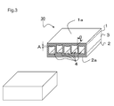
- Fig. 3 is an external perspective view schematically illustrating a state of being cut from the first wall section to the second wall section as still another example of the flow path member according to the present embodiment.
- a central portion of at least one of the first wall section 1 and the second wall section 2 which configures the flow path is curved toward the flow path side.
- Fig. 3 illustrates an example in which both central portions of the first wall section 1 and the second wall section 2 are curved toward the flow path side.
- an angle ⁇ on a corner portion between the first wall section 1 and the third wall section 3 in the flow path is an acute angle. Therefore, compared to a case where the central portion of the first wall section 1 or the second wall section 2 which configures the flow path is not curved toward the flow path, it is possible to cause a direction of the stress produced on the corner not to be toward the corner of the adjacent flow path but to be toward the first wall section 1 side. Accordingly, the stress concentration between the corners of the adjacent flow paths is reduced and it is possible to suppress damage to the flow path. Therefore, the reliability of the flow path member 30 is improved.
- the central portion described here indicates a center part when the width of the flow path opening 4 is equally divided into three parts on the cut plane.
- a degree of the curvature of the first wall section 1 or the second wall section 2 toward the flow path is represented, for example, by a distance from a line connecting corners of the flow path opening 4 on the first wall section 1 side to each other to an end of a perpendicular line at a portion where the first wall section 1 is curved most toward the flow path side as illustrated by the portion A illustrated in Fig. 3 .
- the flow path opening 4 be formed to be within a range of 80% to 99.8% with respect to a height of the flow path opening 4 (distance between the center of a line connecting corners on the first wall section 1 side in the width direction and the center of a line connecting corners on the second wall section 2 side in the width direction in a single flow path opening 4).
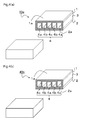
- Fig. 4 is an external perspective view schematically illustrating a state of being cut from the first wall section to the second wall section as still another example of the flow path member according to the present embodiment, (a) illustrates an example in which the flow paths are displaced gradually closer to the first wall section side approaching the center than at the opposite ends, and (b) illustrates an example in which the flow paths are displaced gradually closer to the second wall section side approaching the center than at the opposite ends.
- the flow path openings 4 are disposed to be displaced gradually closer either to the first wall section 1 side or the second wall section 2 side approaching the center than at opposite ends. According to such a configuration, it is possible to reduce the stress concentration between the corners of the adjacent flow paths in all of the flow paths, and to suppress damage to the flow paths. When the temperature is distributed differently throughout the member as the heat exchange target, it is possible to cause the temperature to be nearly uniformly distributed.
- the flow path openings 4a to 4c on the cut plane may be disposed to be displaced gradually closer to the first wall section 1 side approaching the center than at the opposite ends.
- the flow path openings 4a to 4c on the cut plane may be disposed to be displaced gradually closer to the second wall section 2 side approaching the center than at the opposite ends.
- Fig. 5 is an external perspective view schematically illustrating a state of being cut from the first wall section to the second wall section as still another example of the flow path member according to the present embodiment.
- the flow path openings 4a and 4b are disposed to be displaced toward the first wall section 1 side or toward the second wall section 2 side alternately. According to such a configuration, it is possible to reduce the stress concentration between the corners of all the adjacent flow paths. Thus, since it is possible to suppress damage to the flow path, it is possible to improve the reliability of the flow path member 50. Further, it is possible to cause physical behavior to be dispersed from the main surface 1a of the first wall section 1 or from the main surface 2a of the second wall section 2 of the flow path member 50. Thus, since stress concentration due to an external factor is lowered and hence it is possible to suppress damage to the flow path, it is possible to improve the reliability of the flow path member 50.
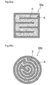
- Fig. 6 shows cross-sectional views illustrating a cross section in parallel to the first wall section and the second wall section as still another example of the flow path member according to the present embodiment, (a) is a meandering flow path, and (b) is a spiralling flow path.
- a plurality of flow paths arranged in one direction on the cut plane is connected in the flow path member 60 and forms one flow path.
- a metal member is provided on at least one surface or in at least one interior section of the first wall section 1 and the second wall section 2 of the flow path members 10, 20, 30, 40, 50, and 60 according to the present embodiment, and thereby a heat exchanger can be formed.
- heat exchanger when a heat generating member is disposed on the main surface 1a or on the main surface 2a on which the metal member is provided, heat produced by the heat generating member is transmitted efficiently to the metal member, and the transmitted heat is further transmitted to the wall sections. Thus, it is possible to efficiently perform heat exchange with the fluid flowing through the flow path. Since the flow path members 10, 20, 30, 40, 50, and 60 according to the present embodiment are highly reliable, the heat exchanger also becomes high in reliability.
- the heat exchanger according to the present embodiment is particularly effective in a case where an electronic component is disposed, which includes a heat generating unit such as an LED element or a power semiconductor as the heat generating member.
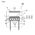
- Fig. 7 is a view illustrating an example of a semiconductor manufacturing device including the heat exchanger according to the present embodiment.
- the semiconductor manufacturing device 200 is a plasma processing device of a wafer W, and the wafer W is mounted on a heat exchanger 100 in which a metal member 11 is provided in the interior section of the first wall section 1 of the flow path members 10, 20, 30, 40, 50, and 60 according to the present embodiment.
- a metal member 11 is provided in the interior section of the first wall section 1 of the flow path members 10, 20, 30, 40, 50, and 60 according to the present embodiment.
- an inlet 62 is connected to a supply tube 64
- an outlet 63 is connected to a discharge tube 65
- a fluid such as a gas or a liquid which is high or low in temperature is caused to circulate through the flow path provided in the flow path members 10, 20, 30, 40, 50, and 60, and thereby heating or cooling of the wafer W is performed.
- an upper electrode 12 for generating plasma is provided above the wafer W
- the metal member 11 in the interior section of the first wall section 1 of the flow path members 10, 20, 30, 40, 50, and 60 which configure the heat exchanger 100 is used as a lower electrode for generating plasma
- a voltage is applied between the metal member 11 which is the lower electrode and the upper electrode 12, and thereby it is possible to cause plasma generated between the metal member 11 which is the lower electrode and the upper electrode 12 to be in contact with the wafer W.
- the heat exchanger 100 includes the flow path members 10, 20, 30, 40, 50, and 60 according to the present embodiment, it is possible to maintain the temperature of the metal member 11 as the lower electrode which becomes high in temperature during the plasma process to be stable.
- the metal member 11 of the semiconductor manufacturing device 200 may be divided into a plurality of members and may be formed to be a bipolar electrode which has one electrode and the other electrode.
- Fig. 7 illustrates an example in which the metal member 11 is used as the lower electrode for generating plasma; however, when the metal member 11 is heated by a current flowing therein, it is possible to control the temperature of the fluid.
- the first wall section 1 is formed of a dielectric material, then the metal member 11 is used as an electrode for electrostatic adsorption, and, when a voltage is applied to the metal member 11, it is possible to adsorb and hold the wafer W with an electrostatic adsorption force such as the Coulomb force or the Johnson Rahbeck force which is generated between the wafer W and the dielectric layer.
- an electrostatic adsorption force such as the Coulomb force or the Johnson Rahbeck force which is generated between the wafer W and the dielectric layer.
- the heat exchanger 100 since the heat exchanger 100 according to the present embodiment includes the metal member 11 provided in the interior section of at least one of the first wall section 1 and the second wall section 2 of the flow path members 10, 20, 30, 40, 50, and 60 according to the present embodiment which are highly reliable, it is possible to achieve the heat exchanger 100 that is high in heat exchange efficiency and in reliability and thus that is durable in a long-term use.
- the semiconductor manufacturing device 200 including the flow path members according to the present embodiment is capable of performing as an appropriate semiconductor manufacturing device which has little trouble when manufacturing or monitoring the semiconductor element.
- examples of the semiconductor manufacturing device 200 according to the present embodiment include, in addition to the plasma processing device illustrated in Fig. 7 as an example thereof, a sputtering device, a resist applying device, a CVD device or an etching process device, and when these devices include the flow path members 10, 20, 30, 40, 50, and 60 according to the present embodiment, it is possible for these device to achieve the above effect.
- the flow path member in manufacturing the flow path member, a process is described, in which, after obtaining molded bodies of the first wall section 1 and a substrate (hereinafter, also simply referred to as a substrate) having a concave section which is integrally formed of the second wall section 2 and the third wall section 3, the first wall section 1 and the substrate are joined by a joining material, and thereby a molded body to become the flow path member is obtained.
- a substrate hereinafter, also simply referred to as a substrate having a concave section which is integrally formed of the second wall section 2 and the third wall section 3
- a ceramic raw material of which a degree of purity is 90% or more and an average particle size is about 1 ⁇ m is prepared, a predetermined amount of a sintering additive, a binder, and a solvent, a dispersant and the like are added to the ceramic raw material, the mixed slurry is spray-dried and granulated using a spray granulation method (spray-drying method), and then a primary raw material is obtained. Next, the spray-dried and granulated primary raw material is put into a predetermined shape of a rubber die, molded by an isostatic pressing method (rubber-pressing method), then the molded body is removed from the rubber die, and a cutting process is performed.
- a spray granulation method spray-drying method
- the molded body to become the substrate is processed to form a concave portion which configures an external appearance or a flow path into a predetermined shape and forms an inlet and an outlet of the fluid.
- a green sheet may be prepared by being manufactured by the isostatic pressing method, a doctor blade method which is a common molding method of ceramics using slurry, or a roll compaction molding method after granulating the slurry. The cutting process is performed such that the molded body is fit into the molded body to become the substrate so as be able to provide a flow path.
- a joining material formed of slurry can be used, which is obtained by weighing and mixing the ceramic raw material, the sintering additive, the binder, the dispersant and the solvent which are used for manufacturing the molded body to become the first wall section 1 and the molded body to become the substrate.
- the joining material is applied to at least one joining portion of the molded body to become the first wall section 1 and the molded body to become the substrate and the two molded bodies are joined to each other, and thereby a joined molded body is obtained, in which the molded body to become the first wall section 1 and the molded body to become the substrate are joined integrally.
- the joined molded body is fired in an atmosphere in accordance with the ceramic raw material and thereby it is possible to obtain the flow path member according to the present embodiment.
- the molded body to become the first wall section 1 and the molded body to become the substrate are fired in an atmosphere in accordance with the ceramic raw material such that sintered bodies of the first wall section 1 and the substrate are obtained. Then, a joining material made of glass is applied on at least one joining portion of the sintered bodies of the first wall section 1 and the substrate such that the sintered bodies are integrally joined, then a heating process is performed, and thereby it is possible to obtain the flow path member according to the present embodiment.
- the flow path member can be formed to include a plurality of inlets and outlets by being fired.
- a green sheet is formed by the doctor blade method which is a common molding method of ceramics using slurry or by the roll compaction molding method after granulating the slurry, and the molded bodies formed into a desired shape by a die may be stacked.
- silicon carbide powder of which an average particle size is 0.5 ⁇ m to 2 ⁇ m and boron carbide and carboxylate as a sintering additive are prepared.
- the powders are weighed to contain, for example, 0.12% by weight to 1.4% by weight of the boron carbide powder, 1% by weight to 3.4% by weight of the carboxylate powder with respect to 100% by weight of the silicon carbide powder and then are mixed.
- the mixed powder, polyvinyl alcohol, polyethylene glycol, binder such as an acrylic resin or a butyral resin, water, and dispersant are put into a ball mill, a tumbling mill, a vibration mill, or a bead mill and are mixed.
- an added amount of the binder is determined such that the molded body has appropriate strength or flexibility and during firing, attachment and detachment of binder for molding is sufficient, and the slurry produced as described above may be used.
- a green sheet may be manufactured by the doctor blade method, or after the slurry is granulated, a green sheet may be manufactured by the roll compaction method.
- the plurality of green sheets may be stacked to form a desired flow path.
- the same slurry as that used for manufacturing the green sheet is applied, as a joining, material on the joining surfaces of the green sheets, the green sheets are stacked, pressed by pressure of substantially 0.5 MPa through a flat plate-like pressurizer and then, is dried at room temperature of substantially 50°C to 70°C for substantially 10 hours to 15 hours.
- the stacked green sheets to become the flow path member are fired in, for example, a known pusher-type or roller-type continuous tunnel furnace and a batch furnace.
- a temperature for firing is different depending on the materials.
- the stacked green sheets may be maintained in an inert gas atmosphere or in a vacuum atmosphere, at a temperature range of 1800°C to 2200°C for 10 minutes to 10 hours, and then may fired at a temperature range of 2200°C to 2350°C for 10 minutes to 20 hours.
- the molded body obtained by any manufacturing method described above is mounted on a shelf which has a bow-like slope, or a weight which has a bow-like slope is placed on the molded body.
- the molded body is fired in a state in which the molded body is bent, and the first wall section 1 side and the second wall section 2 side are subjected to a grinding process or a polishing process such that the position displacement of the flow path may be changed with respect to the main surfaces 1a and 3a of the flow path member.
- aluminum or copper may be formed by a known printing method, or formed by an evaporation method, an aluminum plate or a copper plate may be joined using an active metal method or a brazing method, or a hole may be formed on a first lid section 1 and the hole may be filled with aluminum or copper. It is possible to obtain the heat exchanger 100 by forming as described above.
- the flow path member according to the present embodiment obtained as described above has flow paths of which adjacent flow paths are positioned to be displaced toward the first wall section 1 or toward the second wall section 2, and thereby the stress concentration between the corners of the adjacent flow paths is reduced.
- the semiconductor manufacturing device 200 includes the heat exchanger 100 that has the flow path member according to the present embodiment, and thereby it is possible to perform manufacturing or examining of the highly reliable semiconductor element.
Landscapes
- Engineering & Computer Science (AREA)
- Physics & Mathematics (AREA)
- Thermal Sciences (AREA)
- Mechanical Engineering (AREA)
- General Engineering & Computer Science (AREA)
- Cooling Or The Like Of Semiconductors Or Solid State Devices (AREA)
- Drying Of Semiconductors (AREA)
- Container, Conveyance, Adherence, Positioning, Of Wafer (AREA)
Abstract
Description
- The present invention relates to a flow path member, and a heat exchanger and a semiconductor manufacturing device using the flow path member.
- In general, a flow path member that includes a flow path therein is capable of performing heat exchange with another member that is in contact with the flow path member by causing a fluid to flow through the flow path and,
thereby it is possible to regulate (control) a temperature of the another member that is in contact with the flow path member. - For example, PTL1 discloses a semiconductor apparatus that includes a semiconductor component which includes at least one semiconductor element and a pair of lead frames between which the semiconductor element is interposed and which is molded from a resin by exposing an outer surface of the lead frame, and a ceramic tube which is joined to the outer surface of the pair of lead frames by a joining metal and includes a refrigerant passage.
- PTL 1: Japanese Unexamined Patent Application Publication No.
2008-103623 - However, a problem arises in that, in the semiconductor device of
PTL 1, in a case where pressure of the fluid is set to be high so as to improve heat exchange efficiency between heat generated by the semiconductor element and a fluid which is a refrigerant flowing through the refrigerant passage, stress is concentrated between corners of particularly adjacent refrigerant passages and thus the refrigerant passages are likely to be damaged. - Therefore, the present invention aims to provide a flow path member, and a heat exchanger and a semiconductor manufacturing device using the flow path member, of which reliability is improved.
- The present invention provides a flow path member including: a first wall section; a second wall section; and a third wall section that is provided between the first wall section and the second wall section. An internal section that is configured by the first wall section, the second wall section, and the third wall section becomes a flow path through which a fluid flows and a plurality of flow path openings of the flow path are arranged in one direction on a cut plane obtained by cutting from the first wall section to the second wall section. One of two adjacent flow path openings is disposed to be more displaced than the other either toward the first wall section side or toward the second wall section side.
- The present invention provides a heat exchanger including: a metal member that is provided on at least one surface or in at least one interior section of the first wall section and the second wall section of the flow path member with the above configuration.
- The present invention provides a semiconductor manufacturing device including: a heat exchanger in which a metal member is provided in at least one interior section of the first wall section and the second wall section of the flow path member with the above configuration and the metal member is an electrode for adsorbing a wafer.
- In the flow path member according to the present invention, the stress concentration between corners of the adjacent flow path openings on the cut plane obtained by cutting from the first wall section to the second wall section is reduced and it is possible to suppress the damage to the flow path. Therefore the reliability is improved.
- In addition, in the heat exchanger according to the present invention, it is possible to achieve a heat exchanger which has high heat exchange efficiency and of which the reliability is improved.
- In addition, in the semiconductor manufacturing device according to the present invention, it is possible to achieve a semiconductor manufacturing device which is capable of manufacturing a highly reliable semiconductor element.
-
-
Fig. 1 is an external perspective view schematically illustrating a state of being cut from a first wall section to the second wall section as an example of a flow path member according to the present embodiment. -
Fig. 2 is an external perspective view schematically illustrating a state of being cut from the first wall section to the second wall section as another example of the flow path member according to the present embodiment. -
Fig. 3 is an external perspective view schematically illustrating a state of being cut from the first wall section to the second wall section as still another example of the flow path member according to the present embodiment. -
Fig. 4 is an external perspective view schematically illustrating a state of being cut from the first wall section to the second wall section as still another example of the flow path member according to the present embodiment, (a) illustrates an example in which the flow paths are displaced gradually closer to the first wall section side approaching the center than at the opposite ends, and (b) illustrates an example in which the flow paths are displaced gradually closer to the second wall section side approaching the center than at the opposite ends. -
Fig. 5 is an external perspective view schematically illustrating a state of being cut from the first wall section to the second wall section as still another example of the flow path member according to the present embodiment. -
Fig. 6 shows cross-sectional views illustrating a cross section in parallel to the first wall section and the second wall section as still another example of the flow path member according to the present embodiment, (a) is a meandering flow path, and (b) is a spiralling flow path. -
Fig. 7 is a view illustrating an example of a semiconductor manufacturing device including the heat exchanger according to the present embodiment. - Hereinafter, examples of a flow path member according to the embodiment of the present invention will be described.
-
Fig. 1 is an external perspective view schematically illustrating a state of being cut from a first wall section to the second wall section as an example of a flow path member according to the present embodiment. The same configuration in the following drawings is described by the same reference signs. - A
flow path member 10 according to the present embodiment illustrated inFig. 1 includes afirst wall section 1, asecond wall section 2, and athird wall section 3 that is provided between thefirst wall section 1 and thesecond wall section 2. An internal section that is configured by thefirst wall section 1, thesecond wall section 2, and thethird wall section 3 becomes a flow path through which a fluid flows and a plurality offlow path openings 4 of the flow path are arranged in one direction on a cut plane obtained by cutting from thefirst wall section 1 to the second wall section 2 (hereinafter, simply referred to as a cut plane). Here, it is preferable that a cross-sectional shape of the flow path opening 4 be a polygon and particularly a square. - In the
flow path member 10 according to the present embodiment, one flow path opening 4a of two adjacentflow path openings first wall section 1 side or toward thesecond wall section 2 side. - Thus, since a distance between corners of adjacent flow path openings 4 (in other words, adjacent flow paths on the cut plane) becomes long and stress concentration occurring between the corners of the adjacent flow paths can be reduced, it is possible to suppress damage to the flow path. Thus, reliability of the
flow path member 10 is improved. In theflow path member 10 according to the present embodiment, the flow path may be configured to have a plurality of flow paths, further may be configured to have one flow path as a whole, and a plurality of theflow path openings 4 may be arranged in one direction on an arbitrary cut plane. Accordingly, hereinafter, when there is no specific description, in description of adjacentflow path openings 4 on the cut plane, the flow paths are adjacent in some cases. - Here, in a method of measuring a length of displacement of the
flow path openings 4 from each other, the cross-sectional shape illustrated inFig. 1 is described as an example. First, with a flow path opening 4 that is closest to amain surface 1a of thefirst wall section 1 or amain surface 2a of thesecond wall section 2 as a reference, the length of displacement of the otherflow path openings 4 may be measured. To be more exact, according toFig. 1 , with the second flow path opening 4 from the left which is closest to themain surface 2a side as a reference, differences from the otherflow path openings 4 may be measured. Here, when a perpendicular line to themain surface 2a is drawn from themain surface 2a to the center on a line connecting the opposite corners of each of theflow path openings 4 in a width direction on thesecond wall section 2 side, a difference of the distances of theflow path openings 4 is the length of the displacement. It is possible to measure the length of the displacement on the cut plane of theflow path member 10 using a known optical microscope, microscope, or the like. In order to reduce the stress concentration between the corners of the adjacentflow path openings 4, it is preferable that 0.01 mm or more of the length of the displacement be secured. In addition, in theflow path member 10 illustrated inFig. 1 , the displacement of the flow path means the displacement of the flow path in a direction either toward thefirst wall section 1 side or toward thesecond wall section 2 side and the same is true for the following drawings. - Here, the
flow path member 10 is assumed to be a flow path through which a highly corrosive gas or liquid flows, and thus it is preferable that theflow path member 10 be formed of ceramics such that theflow path member 10 has a good durability or corrosion resistance and is good in insulation. The material examples of the ceramics can include alumina, zirconia, silicon nitride, aluminum nitride, silicon carbide, cordierite, boron carbide, mullite, or a compound thereof. - Particularly, it is preferable that the
flow path member 10 according to the present embodiment be formed of a silicon carbide sintered body with silicon carbide as a main component. Here, the main component means a component which is 80% by weight or more with respect to 100% by weight of the entire components that configures a sintered body. When theflow path member 10 according to the present embodiment is formed of the silicon carbide sintered body with the silicon carbide as the main component, theflow path member 10 has high thermal conductivity in addition to the good durability or corrosion resistance, and thus the heat exchange efficiency is improved. In addition, since the silicon carbide sintered body has lower specific gravity than other ceramics, for example, alumina, it is possible to achieve a light weight in a case where a large-sizedflow path member 10 is needed. - Samples with predetermined sizes are cut out from the
flow path member 10 and it is possible to check the components of theflow path member 10 by an X-ray diffraction method. In addition, it is possible to check the content through performing an energy dispersive X-ray (EDS) analysis by a scanning electron microscope (SEM). In addition, it is possible to check the content by an ICP emission spectrometry or an X-ray fluorescence spectrometry. -
Fig. 2 is an external perspective view schematically illustrating a state of being cut from the first wall section to the second wall section as another example of the flow path member according to the present embodiment. - In the
flow path member 20 according to the present embodiment illustrated inFig. 2 , for all of the plurality offlow path openings 4 on the cut plane, one of the adjacentflow path openings 4 is disposed to be more displaced either toward thefirst wall section 1 side or toward thesecond wall section 2 side than the other. That is, in theflow path member 20 illustrated inFig. 2 , when theflow path openings first wall section 1 side, when theflow path openings first wall section 1 side, when theflow path openings first wall section 1 side, and when theflow path openings first wall section 1 side. - According to such a configuration, it is possible to further reduce the stress concentration between the corners of all the adjacent flow paths on the cut plane. Thus, since it is possible to further suppress damage to the flow path, it is possible to further improve the reliability of the
flow path member 20. -
Fig. 3 is an external perspective view schematically illustrating a state of being cut from the first wall section to the second wall section as still another example of the flow path member according to the present embodiment. - In the
flow path member 30 according to the present embodiment illustrated inFig. 3 , a central portion of at least one of thefirst wall section 1 and thesecond wall section 2 which configures the flow path is curved toward the flow path side.Fig. 3 illustrates an example in which both central portions of thefirst wall section 1 and thesecond wall section 2 are curved toward the flow path side. - According to such a configuration, it is possible to widen a surface area of the flow path. Thus, it is possible to improve the heat exchange efficiency between the member as the heat exchange target and a fluid. Further, for example, in
Fig. 3 , an angle θ on a corner portion between thefirst wall section 1 and thethird wall section 3 in the flow path is an acute angle. Therefore, compared to a case where the central portion of thefirst wall section 1 or thesecond wall section 2 which configures the flow path is not curved toward the flow path, it is possible to cause a direction of the stress produced on the corner not to be toward the corner of the adjacent flow path but to be toward thefirst wall section 1 side. Accordingly, the stress concentration between the corners of the adjacent flow paths is reduced and it is possible to suppress damage to the flow path. Therefore, the reliability of theflow path member 30 is improved. - The central portion described here indicates a center part when the width of the flow path opening 4 is equally divided into three parts on the cut plane. In addition, a degree of the curvature of the
first wall section 1 or thesecond wall section 2 toward the flow path is represented, for example, by a distance from a line connecting corners of the flow path opening 4 on thefirst wall section 1 side to each other to an end of a perpendicular line at a portion where thefirst wall section 1 is curved most toward the flow path side as illustrated by the portion A illustrated inFig. 3 . It is possible to measure the degree of the curvature on the cut plane of theflow path member 30 using the known optical microscope or microscope. It is preferable that the degree of the curvature be 0.01 mm or more in order for the direction of the stress to be toward thefirst wall section 1 or thesecond wall section 2. - In addition, it is preferable that the flow path opening 4 be formed to be within a range of 80% to 99.8% with respect to a height of the flow path opening 4 (distance between the center of a line connecting corners on the
first wall section 1 side in the width direction and the center of a line connecting corners on thesecond wall section 2 side in the width direction in a single flow path opening 4). -
Fig. 4 is an external perspective view schematically illustrating a state of being cut from the first wall section to the second wall section as still another example of the flow path member according to the present embodiment, (a) illustrates an example in which the flow paths are displaced gradually closer to the first wall section side approaching the center than at the opposite ends, and (b) illustrates an example in which the flow paths are displaced gradually closer to the second wall section side approaching the center than at the opposite ends. - In the flow path member 40 according to the present embodiment illustrated in
Fig. 4 , when all of the plurality offlow path openings 4 on the cut plane are viewed, theflow path openings 4 are disposed to be displaced gradually closer either to thefirst wall section 1 side or thesecond wall section 2 side approaching the center than at opposite ends. According to such a configuration, it is possible to reduce the stress concentration between the corners of the adjacent flow paths in all of the flow paths, and to suppress damage to the flow paths. When the temperature is distributed differently throughout the member as the heat exchange target, it is possible to cause the temperature to be nearly uniformly distributed. - For example, in a case where the member as the heat exchange target is provided on the
first wall section 1 and the temperature of the member is higher at the central portion side than at the periphery, as illustrated inFig. 4(a) , theflow path openings 4a to 4c on the cut plane may be disposed to be displaced gradually closer to thefirst wall section 1 side approaching the center than at the opposite ends. In this case, it is possible to reduce the temperature of the member on the central portion side by causing a fluid which is low in temperature to flow through the flow path and it is possible to cause the temperature to be nearly uniformly distributed throughout the member. - Meanwhile, for example, in a case where the member as the heat exchange target is provided on the
first wall section 1 and the temperature of the member is higher at the periphery than at the central portion, as illustrated inFig. 4(b) , theflow path openings 4a to 4c on the cut plane may be disposed to be displaced gradually closer to thesecond wall section 2 side approaching the center than at the opposite ends. In this case, it is possible to reduce the temperature of the member at the periphery side by causing a fluid which is low in temperature to flow through the flow path and it is possible to cause the temperature to be nearly uniformly distributed throughout the member. -
Fig. 5 is an external perspective view schematically illustrating a state of being cut from the first wall section to the second wall section as still another example of the flow path member according to the present embodiment. - In the
flow path member 50 according to the present embodiment illustrated inFig. 5 , when all of the plurality of flow path openings on the cut plane are viewed, theflow path openings first wall section 1 side or toward thesecond wall section 2 side alternately. According to such a configuration, it is possible to reduce the stress concentration between the corners of all the adjacent flow paths. Thus, since it is possible to suppress damage to the flow path, it is possible to improve the reliability of theflow path member 50. Further, it is possible to cause physical behavior to be dispersed from themain surface 1a of thefirst wall section 1 or from themain surface 2a of thesecond wall section 2 of theflow path member 50. Thus, since stress concentration due to an external factor is lowered and hence it is possible to suppress damage to the flow path, it is possible to improve the reliability of theflow path member 50. -
Fig. 6 shows cross-sectional views illustrating a cross section in parallel to the first wall section and the second wall section as still another example of the flow path member according to the present embodiment, (a) is a meandering flow path, and (b) is a spiralling flow path. - In the flow path member 60 according to the present embodiment illustrated in
Fig. 6 , a plurality of flow paths arranged in one direction on the cut plane is connected in the flow path member 60 and forms one flow path. - For example, when one inlet is provided and a fluid is distributed to a plurality of flow paths, the fluid is likely to flow through a flow path where pressure to the fluid is low, and thus there is a concern that heat exchange is performed unevenly. On the other hand, as illustrated in
Fig. 6 , when the flow paths are formed to be connected in the flow path member 60 as a single flow path, it is possible to cause the fluid to flow efficiently through the entire flow path. Accordingly, it is possible to improve the heat exchange efficiency between the member as the heat exchange target and the fluid. In addition, when the flow path is formed as ameandering flow path 5 illustrated inFig. 6(a) or as aspiralling flow path 6 illustrated inFig. 6(b) , it is possible to cause the fluid to stay longer inside the flow path member 60. Therefore, it is possible to perform heat exchange efficiently. - In addition, a metal member is provided on at least one surface or in at least one interior section of the
first wall section 1 and thesecond wall section 2 of theflow path members - In such a heat exchanger, when a heat generating member is disposed on the
main surface 1a or on themain surface 2a on which the metal member is provided, heat produced by the heat generating member is transmitted efficiently to the metal member, and the transmitted heat is further transmitted to the wall sections. Thus, it is possible to efficiently perform heat exchange with the fluid flowing through the flow path. Since theflow path members -
Fig. 7 is a view illustrating an example of a semiconductor manufacturing device including the heat exchanger according to the present embodiment. - In the example, the
semiconductor manufacturing device 200 is a plasma processing device of a wafer W, and the wafer W is mounted on aheat exchanger 100 in which ametal member 11 is provided in the interior section of thefirst wall section 1 of theflow path members flow path members inlet 62 is connected to asupply tube 64, anoutlet 63 is connected to adischarge tube 65, a fluid such as a gas or a liquid which is high or low in temperature is caused to circulate through the flow path provided in theflow path members - In addition, an
upper electrode 12 for generating plasma is provided above the wafer W, themetal member 11 in the interior section of thefirst wall section 1 of theflow path members heat exchanger 100 is used as a lower electrode for generating plasma, a voltage is applied between themetal member 11 which is the lower electrode and theupper electrode 12, and thereby it is possible to cause plasma generated between themetal member 11 which is the lower electrode and theupper electrode 12 to be in contact with the wafer W. Since theheat exchanger 100 includes theflow path members metal member 11 as the lower electrode which becomes high in temperature during the plasma process to be stable. In addition, since the temperature of the wafer W is also controlled, it is possible to perform a highly dimension-accurate process. In addition, themetal member 11 of thesemiconductor manufacturing device 200 may be divided into a plurality of members and may be formed to be a bipolar electrode which has one electrode and the other electrode. - In addition,
Fig. 7 illustrates an example in which themetal member 11 is used as the lower electrode for generating plasma; however, when themetal member 11 is heated by a current flowing therein, it is possible to control the temperature of the fluid. - Further, the
first wall section 1 is formed of a dielectric material, then themetal member 11 is used as an electrode for electrostatic adsorption, and, when a voltage is applied to themetal member 11, it is possible to adsorb and hold the wafer W with an electrostatic adsorption force such as the Coulomb force or the Johnson Rahbeck force which is generated between the wafer W and the dielectric layer. - Thus, since the
heat exchanger 100 according to the present embodiment includes themetal member 11 provided in the interior section of at least one of thefirst wall section 1 and thesecond wall section 2 of theflow path members heat exchanger 100 that is high in heat exchange efficiency and in reliability and thus that is durable in a long-term use. - Since the
flow path members semiconductor manufacturing device 200 including the flow path members according to the present embodiment is capable of performing as an appropriate semiconductor manufacturing device which has little trouble when manufacturing or monitoring the semiconductor element. In addition, examples of thesemiconductor manufacturing device 200 according to the present embodiment include, in addition to the plasma processing device illustrated inFig. 7 as an example thereof, a sputtering device, a resist applying device, a CVD device or an etching process device, and when these devices include theflow path members - Hereinafter, an example of a method of manufacturing the flow path member according to the present embodiment will be described. The following description is provided without reference signs for the flow path member except that the component is specialized as the aspect illustrated in
Figs. 1 to 6 . - First, in manufacturing the flow path member, a process is described, in which, after obtaining molded bodies of the
first wall section 1 and a substrate (hereinafter, also simply referred to as a substrate) having a concave section which is integrally formed of thesecond wall section 2 and thethird wall section 3, thefirst wall section 1 and the substrate are joined by a joining material, and thereby a molded body to become the flow path member is obtained. - A ceramic raw material of which a degree of purity is 90% or more and an average particle size is about 1 µm is prepared, a predetermined amount of a sintering additive, a binder, and a solvent, a dispersant and the like are added to the ceramic raw material, the mixed slurry is spray-dried and granulated using a spray granulation method (spray-drying method), and then a primary raw material is obtained. Next, the spray-dried and granulated primary raw material is put into a predetermined shape of a rubber die, molded by an isostatic pressing method (rubber-pressing method), then the molded body is removed from the rubber die, and a cutting process is performed.
- During the cutting process, the molded body to become the substrate is processed to form a concave portion which configures an external appearance or a flow path into a predetermined shape and forms an inlet and an outlet of the fluid. Next, as the molded body to become the
first wall section 1 of the flow path member, a green sheet may be prepared by being manufactured by the isostatic pressing method, a doctor blade method which is a common molding method of ceramics using slurry, or a roll compaction molding method after granulating the slurry. The cutting process is performed such that the molded body is fit into the molded body to become the substrate so as be able to provide a flow path. - Next, a process of joining the molded body to become the
first wall section 1 to the molded body to become the substrate will be described. As the joining material to be used for joining, a joining material formed of slurry can be used, which is obtained by weighing and mixing the ceramic raw material, the sintering additive, the binder, the dispersant and the solvent which are used for manufacturing the molded body to become thefirst wall section 1 and the molded body to become the substrate. The joining material is applied to at least one joining portion of the molded body to become thefirst wall section 1 and the molded body to become the substrate and the two molded bodies are joined to each other, and thereby a joined molded body is obtained, in which the molded body to become thefirst wall section 1 and the molded body to become the substrate are joined integrally. The joined molded body is fired in an atmosphere in accordance with the ceramic raw material and thereby it is possible to obtain the flow path member according to the present embodiment. - In addition, in another example of a manufacturing method, the molded body to become the
first wall section 1 and the molded body to become the substrate are fired in an atmosphere in accordance with the ceramic raw material such that sintered bodies of thefirst wall section 1 and the substrate are obtained. Then, a joining material made of glass is applied on at least one joining portion of the sintered bodies of thefirst wall section 1 and the substrate such that the sintered bodies are integrally joined, then a heating process is performed, and thereby it is possible to obtain the flow path member according to the present embodiment. - Next, a method of manufacturing the flow path member by an extrusion molding method will be described.
- After a die with a desired shape is prepared and a molded body to become the flow path member is obtained by a known extrusion molding method, the flow path member can be formed to include a plurality of inlets and outlets by being fired.
- In addition, as another example of a process of obtaining a molded body, a green sheet is formed by the doctor blade method which is a common molding method of ceramics using slurry or by the roll compaction molding method after granulating the slurry, and the molded bodies formed into a desired shape by a die may be stacked.
- For example, as one example, as a method of producing the slurry, first, silicon carbide powder of which an average particle size is 0.5 µm to 2 µm and boron carbide and carboxylate as a sintering additive are prepared. The powders are weighed to contain, for example, 0.12% by weight to 1.4% by weight of the boron carbide powder, 1% by weight to 3.4% by weight of the carboxylate powder with respect to 100% by weight of the silicon carbide powder and then are mixed.
- Next, the mixed powder, polyvinyl alcohol, polyethylene glycol, binder such as an acrylic resin or a butyral resin, water, and dispersant are put into a ball mill, a tumbling mill, a vibration mill, or a bead mill and are mixed. Here, an added amount of the binder is determined such that the molded body has appropriate strength or flexibility and during firing, attachment and detachment of binder for molding is sufficient, and the slurry produced as described above may be used.
- The slurry produced as described above is used and a green sheet may be manufactured by the doctor blade method, or after the slurry is granulated, a green sheet may be manufactured by the roll compaction method. The plurality of green sheets may be stacked to form a desired flow path.
- In addition, the same slurry as that used for manufacturing the green sheet is applied, as a joining, material on the joining surfaces of the green sheets, the green sheets are stacked, pressed by pressure of substantially 0.5 MPa through a flat plate-like pressurizer and then, is dried at room temperature of substantially 50°C to 70°C for substantially 10 hours to 15 hours.
- Next, the stacked green sheets to become the flow path member are fired in, for example, a known pusher-type or roller-type continuous tunnel furnace and a batch furnace. A temperature for firing is different depending on the materials. For example, when silicon carbide is a main component, the stacked green sheets may be maintained in an inert gas atmosphere or in a vacuum atmosphere, at a temperature range of 1800°C to 2200°C for 10 minutes to 10 hours, and then may fired at a temperature range of 2200°C to 2350°C for 10 minutes to 20 hours.
- In addition, as another method, for example, during the firing, the molded body obtained by any manufacturing method described above is mounted on a shelf which has a bow-like slope, or a weight which has a bow-like slope is placed on the molded body. In this way, the molded body is fired in a state in which the molded body is bent, and the
first wall section 1 side and thesecond wall section 2 side are subjected to a grinding process or a polishing process such that the position displacement of the flow path may be changed with respect to themain surfaces 1a and 3a of the flow path member. - Here, for example, in order to form the
metal member 11 on at least one of thefirst wall section 1 andsecond wall section 2 of the flow path member, aluminum or copper may be formed by a known printing method, or formed by an evaporation method, an aluminum plate or a copper plate may be joined using an active metal method or a brazing method, or a hole may be formed on afirst lid section 1 and the hole may be filled with aluminum or copper. It is possible to obtain theheat exchanger 100 by forming as described above. - The flow path member according to the present embodiment obtained as described above has flow paths of which adjacent flow paths are positioned to be displaced toward the
first wall section 1 or toward thesecond wall section 2, and thereby the stress concentration between the corners of the adjacent flow paths is reduced. Thus, since the flow path is unlikely to be damaged, it is possible to obtain the flow path member of which the reliability is improved. In addition, particularly, thesemiconductor manufacturing device 200 includes theheat exchanger 100 that has the flow path member according to the present embodiment, and thereby it is possible to perform manufacturing or examining of the highly reliable semiconductor element. -
- 1
- FIRST WALL SECTION
- 1a
- MAIN SURFACE OF THE FIRST WALL SECTION
- 2
- SECOND WALL SECTION
- 2a
- MAIN SURFACE OF THE SECOND WALL SECTION
- 3
- THIRD WALL SECTION
- 4, 4a, 4b, 4c, 4d, 4e
- FLOW PATH OPENING
- 5, 6
- FLOW PATH
- 10, 20, 30, 40, 50, 60
- FLOW PATH MEMBER
- 61
- WAFER
- 62
- INLET
- 63
- OUTLET
- 64
- SUPPLY TUBE
- 65
- DISCHARGE TUBE
- 100
- HEAT EXCHANGER
- 200
- SEMICONDUCTOR MANUFACTURING DEVICE
Claims (7)
- A flow path member comprising:a first wall section;a second wall section; anda third wall section that is provided between the first wall section and the second wall section,wherein an internal section that is configured by the first wall section, the second wall section, and the third wall section becomes a flow path through which a fluid flows and a plurality of flow path openings of the flow path are arranged in one direction on a cut plane obtained by cutting from the first wall section to the second wall section, andwherein one of two adjacent flow path openings is disposed to be more displaced than the other either toward the first wall section side or toward the second wall section side.
- The flow path member according to claim 1,
wherein, among all of the plurality of flow path openings on the cut plane, one of two adjacent flow path openings is disposed to be more displaced than the other either toward the first wall section side or toward the second wall section side. - The flow path member according to claim 1 or 2,
wherein the central portion of at least one of the first wall section and the second wall section that configures the flow path is curved toward the flow path side. - The flow path member according to any one of claims 1 to 3,
wherein the flow path openings are disposed to be displaced gradually closer either to the first wall section side or to the second wall section side approaching the center than at the opposite ends when all of the plurality of flow path openings on the cut plane are viewed. - The flow path member according to any one of claims 1 to 3,
wherein the flow path openings are disposed to be displaced toward the first wall section side or toward the second wall section side alternately when all of the plurality of flow path openings on the cut plane are viewed. - A heat exchanger comprising:a metal member that is provided on at least one surface or in at least one interior section of the first wall section and the second wall section of the flow path member according to any one of claims 1 to 5.
- A semiconductor manufacturing device comprising:a heat exchanger in which a metal member is provided in at least one interior section of the first wall section and the second wall section of the flow path member according to any one of claims 1 to 5 and the metal member is an electrode for adsorbing a wafer.
Applications Claiming Priority (2)
| Application Number | Priority Date | Filing Date | Title |
|---|---|---|---|
| JP2012167200 | 2012-07-27 | ||
| PCT/JP2013/070524 WO2014017661A1 (en) | 2012-07-27 | 2013-07-29 | Flow path member, and heat exchanger and semiconductor manufacturing device using same |
Publications (3)
| Publication Number | Publication Date |
|---|---|
| EP2879162A1 true EP2879162A1 (en) | 2015-06-03 |
| EP2879162A4 EP2879162A4 (en) | 2016-03-23 |
| EP2879162B1 EP2879162B1 (en) | 2020-07-29 |
Family
ID=49997463
Family Applications (1)
| Application Number | Title | Priority Date | Filing Date |
|---|---|---|---|
| EP13822788.9A Active EP2879162B1 (en) | 2012-07-27 | 2013-07-29 | Flow path member, and heat exchanger and semiconductor manufacturing device using same |
Country Status (4)
| Country | Link |
|---|---|
| US (1) | US20150153116A1 (en) |
| EP (1) | EP2879162B1 (en) |
| JP (1) | JP6175437B2 (en) |
| WO (1) | WO2014017661A1 (en) |
Cited By (1)
| Publication number | Priority date | Publication date | Assignee | Title |
|---|---|---|---|---|
| EP4156251A1 (en) * | 2022-08-30 | 2023-03-29 | Ovh | Cooling block for cooling a heat-generating electronic component and method for manufacturing thereof |
Families Citing this family (13)
| Publication number | Priority date | Publication date | Assignee | Title |
|---|---|---|---|---|
| WO2016066392A1 (en) * | 2014-10-28 | 2016-05-06 | Asml Netherlands B.V. | Component for a lithography tool, lithography apparatus, inspection tool and a method of manufacturing a device |
| JP6401012B2 (en) * | 2014-10-28 | 2018-10-03 | 京セラ株式会社 | Ceramic substrate |
| WO2016143033A1 (en) * | 2015-03-09 | 2016-09-15 | ギガフォトン株式会社 | High-voltage pulse generating device |
| JP2017212328A (en) * | 2016-05-25 | 2017-11-30 | 京セラ株式会社 | Ceramic passage member |
| US11848177B2 (en) | 2018-02-23 | 2023-12-19 | Lam Research Corporation | Multi-plate electrostatic chucks with ceramic baseplates |
| CN113439330A (en) * | 2019-02-12 | 2021-09-24 | 朗姆研究公司 | Electrostatic chuck with ceramic monolith |
| WO2021201108A1 (en) * | 2020-03-31 | 2021-10-07 | 京セラ株式会社 | Flow path member and method for manufacturing same |
| EP4050295A1 (en) * | 2021-02-26 | 2022-08-31 | Ovh | Water block having hollow fins |
| US12111120B2 (en) * | 2021-03-17 | 2024-10-08 | Carrier Corporation | Microchannel heat exchanger |
| JP7522089B2 (en) * | 2021-11-10 | 2024-07-24 | 日本碍子株式会社 | Wafer placement table |
| JP7714505B2 (en) * | 2022-01-27 | 2025-07-29 | 日本碍子株式会社 | Wafer mounting table and semiconductor manufacturing equipment component using the same |
| WO2024241516A1 (en) * | 2023-05-24 | 2024-11-28 | 日本碍子株式会社 | Wafer mounting table |
| JP7809404B1 (en) * | 2025-08-29 | 2026-02-02 | 株式会社 Synax | Evaporator, temperature controller and handler |
Family Cites Families (29)
| Publication number | Priority date | Publication date | Assignee | Title |
|---|---|---|---|---|
| US1296916A (en) * | 1918-02-07 | 1919-03-11 | Charles F Burroughs | Heating or cooling plate for molding-presses. |
| US1413571A (en) * | 1920-01-16 | 1922-04-25 | Wilhelm B Bronander | Phonograph-record die holder |
| US3369782A (en) * | 1965-10-05 | 1968-02-20 | Navy Usa | Cooled leading edge |
| US4489570A (en) * | 1982-12-01 | 1984-12-25 | The Board Of Trustees Of The Leland Stanford Junior University | Fast cooldown miniature refrigerators |
| JPS62229947A (en) * | 1986-03-31 | 1987-10-08 | Tokuda Seisakusho Ltd | Dry etching device |
| GB8627981D0 (en) * | 1986-11-22 | 1986-12-31 | Howard Ind Pipework Services L | Furnace panel |
| JPH0284251A (en) * | 1988-06-10 | 1990-03-26 | Matsushita Seiko Co Ltd | Heat exchanger tube and its manufacturing method |
| US5111280A (en) * | 1988-11-10 | 1992-05-05 | Iversen Arthur H | Thermal management of power conditioning systems |
| US5003376A (en) * | 1989-03-28 | 1991-03-26 | Coriolis Corporation | Cooling of large high power semi-conductors |
| JPH11329926A (en) * | 1998-05-11 | 1999-11-30 | Dainippon Screen Mfg Co Ltd | Substrate cooling device and substrate cooling method |
| JP2000266484A (en) * | 1999-03-17 | 2000-09-29 | Bosch Automotive Systems Corp | Heat exchanger |
| JP4209057B2 (en) * | 1999-12-01 | 2009-01-14 | 東京エレクトロン株式会社 | Ceramic heater, substrate processing apparatus and substrate processing method using the same |
| JP2001165532A (en) * | 1999-12-09 | 2001-06-22 | Denso Corp | Refrigerant condenser |
| JP4312339B2 (en) * | 2000-02-24 | 2009-08-12 | ナブテスコ株式会社 | Heat transfer device with meandering passage |
| JP4697833B2 (en) * | 2000-06-14 | 2011-06-08 | キヤノンアネルバ株式会社 | Electrostatic adsorption mechanism and surface treatment apparatus |
| KR100382523B1 (en) * | 2000-12-01 | 2003-05-09 | 엘지전자 주식회사 | a tube structure of a micro-multi channel heat exchanger |
| JP3945208B2 (en) * | 2001-10-09 | 2007-07-18 | 株式会社デンソー | Heat exchange tubes and heat exchangers |
| US20070130769A1 (en) * | 2002-09-03 | 2007-06-14 | Moon Seok H | Micro heat pipe with pligonal cross-section manufactured via extrusion or drawing |
| US20040187787A1 (en) * | 2003-03-31 | 2004-09-30 | Dawson Keith E. | Substrate support having temperature controlled substrate support surface |
| JP4942364B2 (en) * | 2005-02-24 | 2012-05-30 | 京セラ株式会社 | Electrostatic chuck, wafer holding member, and wafer processing method |
| DE202005015627U1 (en) * | 2005-09-28 | 2007-02-08 | Autokühler GmbH & Co. KG | Heat exchanger network and thus equipped heat exchanger |
| DE102005052683B4 (en) * | 2005-10-27 | 2012-05-31 | Visteon Global Technologies Inc. | Multi-channel flat tube for heat exchangers |
| JP2007251002A (en) * | 2006-03-17 | 2007-09-27 | Toshiba Corp | Heat sink, electronic device, method of manufacturing heat sink, and method of manufacturing electronic device |
| US8757246B2 (en) * | 2006-06-06 | 2014-06-24 | Raytheon Company | Heat sink and method of making same |
| JP4826426B2 (en) | 2006-10-20 | 2011-11-30 | 株式会社デンソー | Semiconductor device |
| US20090159253A1 (en) * | 2007-12-21 | 2009-06-25 | Zaiqian Hu | Heat exchanger tubes and combo-coolers including the same |
| JP2010143110A (en) * | 2008-12-19 | 2010-07-01 | Sii Printek Inc | Head chip, liquid ejection head, and liquid ejector |
| US8608852B2 (en) * | 2010-06-11 | 2013-12-17 | Applied Materials, Inc. | Temperature controlled plasma processing chamber component with zone dependent thermal efficiencies |
| JP2013011362A (en) * | 2011-06-28 | 2013-01-17 | Kyocera Corp | Circulation hole member, and method for manufacturing circulation hole member |
-
2013
- 2013-07-29 JP JP2014527043A patent/JP6175437B2/en active Active
- 2013-07-29 EP EP13822788.9A patent/EP2879162B1/en active Active
- 2013-07-29 US US14/415,674 patent/US20150153116A1/en not_active Abandoned
- 2013-07-29 WO PCT/JP2013/070524 patent/WO2014017661A1/en not_active Ceased
Cited By (1)
| Publication number | Priority date | Publication date | Assignee | Title |
|---|---|---|---|---|
| EP4156251A1 (en) * | 2022-08-30 | 2023-03-29 | Ovh | Cooling block for cooling a heat-generating electronic component and method for manufacturing thereof |
Also Published As
| Publication number | Publication date |
|---|---|
| JP6175437B2 (en) | 2017-08-02 |
| WO2014017661A1 (en) | 2014-01-30 |
| JPWO2014017661A1 (en) | 2016-07-11 |
| EP2879162A4 (en) | 2016-03-23 |
| US20150153116A1 (en) | 2015-06-04 |
| EP2879162B1 (en) | 2020-07-29 |
Similar Documents
| Publication | Publication Date | Title |
|---|---|---|
| EP2879162B1 (en) | Flow path member, and heat exchanger and semiconductor manufacturing device using same | |
| EP2857786B1 (en) | Flow path member, and heat exchanger and semiconductor manufacturing apparatus using same | |
| EP2772717B1 (en) | Channel member, heat exchanger, and semiconductor unit including the same | |
| EP1211725A1 (en) | Electrostatic chuck | |
| EP1422754A1 (en) | Ceramic joint body | |
| JP6162558B2 (en) | Channel member, heat exchanger using the same, and semiconductor manufacturing apparatus | |
| KR20040068154A (en) | Ceramic heater | |
| WO2003007661A1 (en) | Ceramic heater and ceramic joined article | |
| EP1340732A1 (en) | Aluminum nitride sintered body, method for producing aluminum nitride sintered body, ceramic substrate and method for producing ceramic substrate | |
| WO2001097264A1 (en) | Hot plate | |
| US10103047B2 (en) | Flow path member, heat exchanger including the flow path member, and semiconductor manufacturing apparatus including the flow path member | |
| US9953898B2 (en) | Flow channel member, and heat exchanger and semiconductor module each using same | |
| EP3041039B1 (en) | Sample-retainer | |
| JP2005032842A (en) | Electrode structure and ceramic joint | |
| JP2002134600A (en) | Electrostatic chuck | |
| JP6154248B2 (en) | Channel member, heat exchanger using the same, and semiconductor manufacturing apparatus | |
| JP6290635B2 (en) | Channel member, heat exchanger using the same, and semiconductor manufacturing apparatus | |
| JP6419030B2 (en) | Channel member, heat exchanger using the same, and semiconductor manufacturing apparatus | |
| JP2003146770A (en) | Ceramic joined body | |
| JP2017212328A (en) | Ceramic passage member |
Legal Events
| Date | Code | Title | Description |
|---|---|---|---|
| PUAI | Public reference made under article 153(3) epc to a published international application that has entered the european phase |
Free format text: ORIGINAL CODE: 0009012 |
|
| 17P | Request for examination filed |
Effective date: 20141223 |
|
| AK | Designated contracting states |
Kind code of ref document: A1 Designated state(s): AL AT BE BG CH CY CZ DE DK EE ES FI FR GB GR HR HU IE IS IT LI LT LU LV MC MK MT NL NO PL PT RO RS SE SI SK SM TR |
|
| AX | Request for extension of the european patent |
Extension state: BA ME |
|
| DAX | Request for extension of the european patent (deleted) | ||
| REG | Reference to a national code |
Ref country code: DE Ref legal event code: R079 Ref document number: 602013071188 Country of ref document: DE Free format text: PREVIOUS MAIN CLASS: H01L0021020000 Ipc: H01L0023473000 |
|
| RA4 | Supplementary search report drawn up and despatched (corrected) |
Effective date: 20160224 |
|
| RIC1 | Information provided on ipc code assigned before grant |
Ipc: H01L 21/67 20060101ALI20160218BHEP Ipc: F28F 13/06 20060101ALI20160218BHEP Ipc: H01L 23/473 20060101AFI20160218BHEP |
|
| GRAP | Despatch of communication of intention to grant a patent |
Free format text: ORIGINAL CODE: EPIDOSNIGR1 |
|
| STAA | Information on the status of an ep patent application or granted ep patent |
Free format text: STATUS: GRANT OF PATENT IS INTENDED |
|
| INTG | Intention to grant announced |
Effective date: 20200220 |
|
| GRAS | Grant fee paid |
Free format text: ORIGINAL CODE: EPIDOSNIGR3 |
|
| GRAA | (expected) grant |
Free format text: ORIGINAL CODE: 0009210 |
|
| STAA | Information on the status of an ep patent application or granted ep patent |
Free format text: STATUS: THE PATENT HAS BEEN GRANTED |
|
| AK | Designated contracting states |
Kind code of ref document: B1 Designated state(s): AL AT BE BG CH CY CZ DE DK EE ES FI FR GB GR HR HU IE IS IT LI LT LU LV MC MK MT NL NO PL PT RO RS SE SI SK SM TR |
|
| REG | Reference to a national code |
Ref country code: CH Ref legal event code: EP |
|
| REG | Reference to a national code |
Ref country code: AT Ref legal event code: REF Ref document number: 1296800 Country of ref document: AT Kind code of ref document: T Effective date: 20200815 |
|
| REG | Reference to a national code |
Ref country code: IE Ref legal event code: FG4D |
|
| REG | Reference to a national code |
Ref country code: DE Ref legal event code: R096 Ref document number: 602013071188 Country of ref document: DE |
|
| REG | Reference to a national code |
Ref country code: SE Ref legal event code: TRGR |
|
| REG | Reference to a national code |
Ref country code: LT Ref legal event code: MG4D |
|
| REG | Reference to a national code |
Ref country code: NL Ref legal event code: MP Effective date: 20200729 |
|
| REG | Reference to a national code |
Ref country code: AT Ref legal event code: MK05 Ref document number: 1296800 Country of ref document: AT Kind code of ref document: T Effective date: 20200729 |
|
| PG25 | Lapsed in a contracting state [announced via postgrant information from national office to epo] |
Ref country code: HR Free format text: LAPSE BECAUSE OF FAILURE TO SUBMIT A TRANSLATION OF THE DESCRIPTION OR TO PAY THE FEE WITHIN THE PRESCRIBED TIME-LIMIT Effective date: 20200729 Ref country code: PT Free format text: LAPSE BECAUSE OF FAILURE TO SUBMIT A TRANSLATION OF THE DESCRIPTION OR TO PAY THE FEE WITHIN THE PRESCRIBED TIME-LIMIT Effective date: 20201130 Ref country code: BG Free format text: LAPSE BECAUSE OF FAILURE TO SUBMIT A TRANSLATION OF THE DESCRIPTION OR TO PAY THE FEE WITHIN THE PRESCRIBED TIME-LIMIT Effective date: 20201029 Ref country code: ES Free format text: LAPSE BECAUSE OF FAILURE TO SUBMIT A TRANSLATION OF THE DESCRIPTION OR TO PAY THE FEE WITHIN THE PRESCRIBED TIME-LIMIT Effective date: 20200729 Ref country code: NO Free format text: LAPSE BECAUSE OF FAILURE TO SUBMIT A TRANSLATION OF THE DESCRIPTION OR TO PAY THE FEE WITHIN THE PRESCRIBED TIME-LIMIT Effective date: 20201029 Ref country code: AT Free format text: LAPSE BECAUSE OF FAILURE TO SUBMIT A TRANSLATION OF THE DESCRIPTION OR TO PAY THE FEE WITHIN THE PRESCRIBED TIME-LIMIT Effective date: 20200729 Ref country code: LT Free format text: LAPSE BECAUSE OF FAILURE TO SUBMIT A TRANSLATION OF THE DESCRIPTION OR TO PAY THE FEE WITHIN THE PRESCRIBED TIME-LIMIT Effective date: 20200729 Ref country code: GR Free format text: LAPSE BECAUSE OF FAILURE TO SUBMIT A TRANSLATION OF THE DESCRIPTION OR TO PAY THE FEE WITHIN THE PRESCRIBED TIME-LIMIT Effective date: 20201030 Ref country code: FI Free format text: LAPSE BECAUSE OF FAILURE TO SUBMIT A TRANSLATION OF THE DESCRIPTION OR TO PAY THE FEE WITHIN THE PRESCRIBED TIME-LIMIT Effective date: 20200729 |
|
| PG25 | Lapsed in a contracting state [announced via postgrant information from national office to epo] |
Ref country code: IS Free format text: LAPSE BECAUSE OF FAILURE TO SUBMIT A TRANSLATION OF THE DESCRIPTION OR TO PAY THE FEE WITHIN THE PRESCRIBED TIME-LIMIT Effective date: 20201129 Ref country code: LV Free format text: LAPSE BECAUSE OF FAILURE TO SUBMIT A TRANSLATION OF THE DESCRIPTION OR TO PAY THE FEE WITHIN THE PRESCRIBED TIME-LIMIT Effective date: 20200729 Ref country code: RS Free format text: LAPSE BECAUSE OF FAILURE TO SUBMIT A TRANSLATION OF THE DESCRIPTION OR TO PAY THE FEE WITHIN THE PRESCRIBED TIME-LIMIT Effective date: 20200729 Ref country code: PL Free format text: LAPSE BECAUSE OF FAILURE TO SUBMIT A TRANSLATION OF THE DESCRIPTION OR TO PAY THE FEE WITHIN THE PRESCRIBED TIME-LIMIT Effective date: 20200729 |
|
| REG | Reference to a national code |
Ref country code: CH Ref legal event code: PL |
|
| PG25 | Lapsed in a contracting state [announced via postgrant information from national office to epo] |
Ref country code: NL Free format text: LAPSE BECAUSE OF FAILURE TO SUBMIT A TRANSLATION OF THE DESCRIPTION OR TO PAY THE FEE WITHIN THE PRESCRIBED TIME-LIMIT Effective date: 20200729 |
|
| REG | Reference to a national code |
Ref country code: BE Ref legal event code: MM Effective date: 20200731 |
|
| PG25 | Lapsed in a contracting state [announced via postgrant information from national office to epo] |
Ref country code: LU Free format text: LAPSE BECAUSE OF NON-PAYMENT OF DUE FEES Effective date: 20200729 Ref country code: MC Free format text: LAPSE BECAUSE OF FAILURE TO SUBMIT A TRANSLATION OF THE DESCRIPTION OR TO PAY THE FEE WITHIN THE PRESCRIBED TIME-LIMIT Effective date: 20200729 Ref country code: RO Free format text: LAPSE BECAUSE OF FAILURE TO SUBMIT A TRANSLATION OF THE DESCRIPTION OR TO PAY THE FEE WITHIN THE PRESCRIBED TIME-LIMIT Effective date: 20200729 Ref country code: SM Free format text: LAPSE BECAUSE OF FAILURE TO SUBMIT A TRANSLATION OF THE DESCRIPTION OR TO PAY THE FEE WITHIN THE PRESCRIBED TIME-LIMIT Effective date: 20200729 Ref country code: EE Free format text: LAPSE BECAUSE OF FAILURE TO SUBMIT A TRANSLATION OF THE DESCRIPTION OR TO PAY THE FEE WITHIN THE PRESCRIBED TIME-LIMIT Effective date: 20200729 Ref country code: CH Free format text: LAPSE BECAUSE OF NON-PAYMENT OF DUE FEES Effective date: 20200731 Ref country code: DK Free format text: LAPSE BECAUSE OF FAILURE TO SUBMIT A TRANSLATION OF THE DESCRIPTION OR TO PAY THE FEE WITHIN THE PRESCRIBED TIME-LIMIT Effective date: 20200729 Ref country code: CZ Free format text: LAPSE BECAUSE OF FAILURE TO SUBMIT A TRANSLATION OF THE DESCRIPTION OR TO PAY THE FEE WITHIN THE PRESCRIBED TIME-LIMIT Effective date: 20200729 Ref country code: LI Free format text: LAPSE BECAUSE OF NON-PAYMENT OF DUE FEES Effective date: 20200731 Ref country code: IT Free format text: LAPSE BECAUSE OF FAILURE TO SUBMIT A TRANSLATION OF THE DESCRIPTION OR TO PAY THE FEE WITHIN THE PRESCRIBED TIME-LIMIT Effective date: 20200729 |
|
| REG | Reference to a national code |
Ref country code: DE Ref legal event code: R097 Ref document number: 602013071188 Country of ref document: DE |
|
| PG25 | Lapsed in a contracting state [announced via postgrant information from national office to epo] |
Ref country code: BE Free format text: LAPSE BECAUSE OF NON-PAYMENT OF DUE FEES Effective date: 20200731 Ref country code: AL Free format text: LAPSE BECAUSE OF FAILURE TO SUBMIT A TRANSLATION OF THE DESCRIPTION OR TO PAY THE FEE WITHIN THE PRESCRIBED TIME-LIMIT Effective date: 20200729 |
|
| PLBE | No opposition filed within time limit |
Free format text: ORIGINAL CODE: 0009261 |
|
| STAA | Information on the status of an ep patent application or granted ep patent |
Free format text: STATUS: NO OPPOSITION FILED WITHIN TIME LIMIT |
|
| GBPC | Gb: european patent ceased through non-payment of renewal fee |
Effective date: 20201029 |
|
| PG25 | Lapsed in a contracting state [announced via postgrant information from national office to epo] |
Ref country code: SK Free format text: LAPSE BECAUSE OF FAILURE TO SUBMIT A TRANSLATION OF THE DESCRIPTION OR TO PAY THE FEE WITHIN THE PRESCRIBED TIME-LIMIT Effective date: 20200729 |
|
| 26N | No opposition filed |
Effective date: 20210430 |
|
| PG25 | Lapsed in a contracting state [announced via postgrant information from national office to epo] |
Ref country code: GB Free format text: LAPSE BECAUSE OF NON-PAYMENT OF DUE FEES Effective date: 20201029 Ref country code: IE Free format text: LAPSE BECAUSE OF NON-PAYMENT OF DUE FEES Effective date: 20200729 Ref country code: SI Free format text: LAPSE BECAUSE OF FAILURE TO SUBMIT A TRANSLATION OF THE DESCRIPTION OR TO PAY THE FEE WITHIN THE PRESCRIBED TIME-LIMIT Effective date: 20200729 |
|
| PG25 | Lapsed in a contracting state [announced via postgrant information from national office to epo] |
Ref country code: TR Free format text: LAPSE BECAUSE OF FAILURE TO SUBMIT A TRANSLATION OF THE DESCRIPTION OR TO PAY THE FEE WITHIN THE PRESCRIBED TIME-LIMIT Effective date: 20200729 Ref country code: MT Free format text: LAPSE BECAUSE OF FAILURE TO SUBMIT A TRANSLATION OF THE DESCRIPTION OR TO PAY THE FEE WITHIN THE PRESCRIBED TIME-LIMIT Effective date: 20200729 Ref country code: CY Free format text: LAPSE BECAUSE OF FAILURE TO SUBMIT A TRANSLATION OF THE DESCRIPTION OR TO PAY THE FEE WITHIN THE PRESCRIBED TIME-LIMIT Effective date: 20200729 |
|
| PG25 | Lapsed in a contracting state [announced via postgrant information from national office to epo] |
Ref country code: MK Free format text: LAPSE BECAUSE OF FAILURE TO SUBMIT A TRANSLATION OF THE DESCRIPTION OR TO PAY THE FEE WITHIN THE PRESCRIBED TIME-LIMIT Effective date: 20200729 |
|
| P01 | Opt-out of the competence of the unified patent court (upc) registered |
Effective date: 20230508 |
|
| PGFP | Annual fee paid to national office [announced via postgrant information from national office to epo] |
Ref country code: FR Payment date: 20250610 Year of fee payment: 13 |
|
| PGFP | Annual fee paid to national office [announced via postgrant information from national office to epo] |
Ref country code: SE Payment date: 20250610 Year of fee payment: 13 |
|
| PGFP | Annual fee paid to national office [announced via postgrant information from national office to epo] |
Ref country code: DE Payment date: 20250604 Year of fee payment: 13 |
|
| REG | Reference to a national code |
Ref country code: DE Ref legal event code: R079 Ref document number: 602013071188 Country of ref document: DE Free format text: PREVIOUS MAIN CLASS: H01L0023473000 Ipc: H10W0040470000 |