EP2879157A1 - Charged-particle microscopy with enhanced electron detection - Google Patents
Charged-particle microscopy with enhanced electron detection Download PDFInfo
- Publication number
- EP2879157A1 EP2879157A1 EP14195296.0A EP14195296A EP2879157A1 EP 2879157 A1 EP2879157 A1 EP 2879157A1 EP 14195296 A EP14195296 A EP 14195296A EP 2879157 A1 EP2879157 A1 EP 2879157A1
- Authority
- EP
- European Patent Office
- Prior art keywords
- sample
- map
- electrons
- detector
- image
- Prior art date
- Legal status (The legal status is an assumption and is not a legal conclusion. Google has not performed a legal analysis and makes no representation as to the accuracy of the status listed.)
- Granted
Links
Images


Classifications
-
- H—ELECTRICITY
- H01—ELECTRIC ELEMENTS
- H01J—ELECTRIC DISCHARGE TUBES OR DISCHARGE LAMPS
- H01J37/00—Discharge tubes with provision for introducing objects or material to be exposed to the discharge, e.g. for the purpose of examination or processing thereof
- H01J37/02—Details
- H01J37/244—Detectors; Associated components or circuits therefor
-
- H—ELECTRICITY
- H01—ELECTRIC ELEMENTS
- H01J—ELECTRIC DISCHARGE TUBES OR DISCHARGE LAMPS
- H01J37/00—Discharge tubes with provision for introducing objects or material to be exposed to the discharge, e.g. for the purpose of examination or processing thereof
- H01J37/02—Details
- H01J37/22—Optical, image processing or photographic arrangements associated with the tube
-
- G—PHYSICS
- G01—MEASURING; TESTING
- G01N—INVESTIGATING OR ANALYSING MATERIALS BY DETERMINING THEIR CHEMICAL OR PHYSICAL PROPERTIES
- G01N23/00—Investigating or analysing materials by the use of wave or particle radiation, e.g. X-rays or neutrons, not covered by groups G01N3/00 – G01N17/00, G01N21/00 or G01N22/00
- G01N23/22—Investigating or analysing materials by the use of wave or particle radiation, e.g. X-rays or neutrons, not covered by groups G01N3/00 – G01N17/00, G01N21/00 or G01N22/00 by measuring secondary emission from the material
- G01N23/225—Investigating or analysing materials by the use of wave or particle radiation, e.g. X-rays or neutrons, not covered by groups G01N3/00 – G01N17/00, G01N21/00 or G01N22/00 by measuring secondary emission from the material using electron or ion
-
- H—ELECTRICITY
- H01—ELECTRIC ELEMENTS
- H01J—ELECTRIC DISCHARGE TUBES OR DISCHARGE LAMPS
- H01J37/00—Discharge tubes with provision for introducing objects or material to be exposed to the discharge, e.g. for the purpose of examination or processing thereof
- H01J37/02—Details
- H01J37/22—Optical, image processing or photographic arrangements associated with the tube
- H01J37/222—Image processing arrangements associated with the tube
-
- H—ELECTRICITY
- H01—ELECTRIC ELEMENTS
- H01J—ELECTRIC DISCHARGE TUBES OR DISCHARGE LAMPS
- H01J37/00—Discharge tubes with provision for introducing objects or material to be exposed to the discharge, e.g. for the purpose of examination or processing thereof
- H01J37/26—Electron or ion microscopes; Electron or ion diffraction tubes
-
- H—ELECTRICITY
- H01—ELECTRIC ELEMENTS
- H01J—ELECTRIC DISCHARGE TUBES OR DISCHARGE LAMPS
- H01J37/00—Discharge tubes with provision for introducing objects or material to be exposed to the discharge, e.g. for the purpose of examination or processing thereof
- H01J37/26—Electron or ion microscopes; Electron or ion diffraction tubes
- H01J37/261—Details
- H01J37/265—Controlling the tube; circuit arrangements adapted to a particular application not otherwise provided, e.g. bright-field-dark-field illumination
-
- H—ELECTRICITY
- H01—ELECTRIC ELEMENTS
- H01J—ELECTRIC DISCHARGE TUBES OR DISCHARGE LAMPS
- H01J37/00—Discharge tubes with provision for introducing objects or material to be exposed to the discharge, e.g. for the purpose of examination or processing thereof
- H01J37/26—Electron or ion microscopes; Electron or ion diffraction tubes
- H01J37/28—Electron or ion microscopes; Electron or ion diffraction tubes with scanning beams
-
- G—PHYSICS
- G01—MEASURING; TESTING
- G01N—INVESTIGATING OR ANALYSING MATERIALS BY DETERMINING THEIR CHEMICAL OR PHYSICAL PROPERTIES
- G01N2223/00—Investigating materials by wave or particle radiation
- G01N2223/40—Imaging
- G01N2223/418—Imaging electron microscope
-
- H—ELECTRICITY
- H01—ELECTRIC ELEMENTS
- H01J—ELECTRIC DISCHARGE TUBES OR DISCHARGE LAMPS
- H01J2237/00—Discharge tubes exposing object to beam, e.g. for analysis treatment, etching, imaging
- H01J2237/153—Correcting image defects, e.g. stigmators
-
- H—ELECTRICITY
- H01—ELECTRIC ELEMENTS
- H01J—ELECTRIC DISCHARGE TUBES OR DISCHARGE LAMPS
- H01J2237/00—Discharge tubes exposing object to beam, e.g. for analysis treatment, etching, imaging
- H01J2237/22—Treatment of data
- H01J2237/221—Image processing
-
- H—ELECTRICITY
- H01—ELECTRIC ELEMENTS
- H01J—ELECTRIC DISCHARGE TUBES OR DISCHARGE LAMPS
- H01J2237/00—Discharge tubes exposing object to beam, e.g. for analysis treatment, etching, imaging
- H01J2237/244—Detection characterized by the detecting means
- H01J2237/2441—Semiconductor detectors, e.g. diodes
-
- H—ELECTRICITY
- H01—ELECTRIC ELEMENTS
- H01J—ELECTRIC DISCHARGE TUBES OR DISCHARGE LAMPS
- H01J2237/00—Discharge tubes exposing object to beam, e.g. for analysis treatment, etching, imaging
- H01J2237/244—Detection characterized by the detecting means
- H01J2237/24495—Signal processing, e.g. mixing of two or more signals
-
- H—ELECTRICITY
- H01—ELECTRIC ELEMENTS
- H01J—ELECTRIC DISCHARGE TUBES OR DISCHARGE LAMPS
- H01J2237/00—Discharge tubes exposing object to beam, e.g. for analysis treatment, etching, imaging
- H01J2237/26—Electron or ion microscopes
- H01J2237/28—Scanning microscopes
- H01J2237/2803—Scanning microscopes characterised by the imaging method
- H01J2237/2804—Scattered primary beam
-
- H—ELECTRICITY
- H01—ELECTRIC ELEMENTS
- H01J—ELECTRIC DISCHARGE TUBES OR DISCHARGE LAMPS
- H01J2237/00—Discharge tubes exposing object to beam, e.g. for analysis treatment, etching, imaging
- H01J2237/26—Electron or ion microscopes
- H01J2237/28—Scanning microscopes
- H01J2237/2813—Scanning microscopes characterised by the application
Definitions
- the invention relates to a method of investigating a flux of output electrons emanating from a sample in a charged-particle microscope, which flux is produced in response to irradiation of the sample by a beam of input charged particles.
- the invention additionally relates to a charged-particle microscope comprising:
- Charged-particle microscopy is a well-known and increasingly important technique for imaging microscopic objects, particularly in the form of electron microscopy.
- the basic genus of electron microscope has undergone evolution into a number of well-known apparatus species, such as the Transmission Electron Microscope (TEM), Scanning Electron Microscope (SEM), and Scanning Transmission Electron Microscope (STEM), and also into various sub-species, such as so-called “dual-beam” tools (e.g. a FIB-SEM), which additionally employ a "machining" Focused Ion Beam (FIB), allowing supportive activities such as ion-beam milling or Ion-Beam-Induced Deposition (IBID), for example.
- TEM Transmission Electron Microscope
- SEM Scanning Electron Microscope
- STEM Scanning Transmission Electron Microscope
- FIB-SEM dual-beam
- FIB Focused Ion Beam
- supportive activities such as ion-beam milling
- the electron beam used to irradiate a sample will generally be of significantly higher energy than in the case of a SEM (e.g. 300 keV vs. 10 keV), so as to allow its constituent electrons to penetrate the full depth of the sample; for related reasons, a sample investigated in a TEM will also generally need to be thinner than one investigated in a SEM.
- the imaging beam is "on" for an extended period of time during a given imaging session; however, electron microscopes are also available in which imaging occurs on the basis of a relatively short “flash” or "burst" of electrons, such an approach being of potential benefit when attempting to image moving samples or radiation-sensitive specimens, for example.
- output radiation may, for example, comprise electrons (including so-called Secondary Electrons and/or Backscattered Electrons), visible/infrared/ultraviolet light (fluorescence and cathodoluminescence) and X-rays.
- electrons including so-called Secondary Electrons and/or Backscattered Electrons
- visible/infrared/ultraviolet light fluorescence and cathodoluminescence
- X-rays X-rays.
- the current invention exploits the insight that the statistical nature of the electron emission process set forth above can be exploited advantageously rather than being regarded as a nuisance.
- the inventors took the unusual step of recording multiple images of a sample - not for conventional noise reduction purposes, but to act purely as a basis to perform statistical analysis. This might generally be considered as counter-productive, e.g. in terms of throughput penalty and generally increased radiation dose to the sample.
- S statistical averages/means
- ⁇ 2 S variances
- the accuracy of the procedure set forth in the previous paragraph will depend inter alia on the number M of accumulated images I j , i.e. on the cardinality M of the set ⁇ I j ⁇ . This is a matter of choice, and the skilled artisan will be able to decide how to manage the tradeoff between greater accuracy (in the calculated values of S and ⁇ S ) on the one hand, and the competing issue of throughput on the other hand.
- Another issue that may need to be considered is the total radiation dose delivered to the sample, and an acceptable upper limit in this regard may place a restriction on the value of M .
- the flux of output electrons comprises BS electrons.
- BS electrons lend themselves particularly to application of the statistical processing approach of the present invention because they tend to have a relatively large energy spread. Moreover, they tend to yield better detection contrast than secondary electrons, for example.
- the relatively high energy of BS electrons (as compared to secondary electrons) makes them relatively easy to detect vis-à-vis the typical detection threshold of commonly employed detectors.
- the employed detector is a solid state detector.
- Solid state detectors have certain advantages over more conventional dynode-based PMTs. For example, the former have good linearity in detected energy, and tend to be (much) smaller and cheaper than the latter. In addition, the former can, if desired, be relatively easily embodied as integrated pixelated detectors, which is not possible for the latter. In the context of such solid state detectors, the inventors have achieved particularly good results for the current invention with detectors that employ boron-doped detection cells (such as a delta-doped boron p + n photodiode, for example).
- Such boron-doped detectors are advantageous inter alia in that they are relatively sensitive and highly linear, even for electron energies as low as ca. 200eV.
- More information can, for example, be gleaned from the following technical journal links:
- FIG. 1 is a highly schematic depiction of a charged-particle microscope 400, which, in this case, is a SEM.
- the microscope 400 comprises a particle-optical column 402, which produces a beam 404 of input charged particles (in this case, an electron beam).
- the particle-optical column 402 is mounted on a vacuum chamber 406, which comprises a sample holder / stage 408 for holding a sample 410.
- the vacuum chamber 406 is evacuated using vacuum pumps (not depicted). With the aid of voltage source 422, the sample holder 408, or at least the sample 410, may, if desired, be biased (floated) to an electrical potential with respect to ground.
- the particle-optical column 402 comprises an electron source 412 (such as a Schottky gun), lenses 414, 416 to focus the electron beam 404 onto the sample 410, and a deflection unit 418 (to perform beam steering / scanning of the beam 404).
- the apparatus 400 further comprises a controller / computer processing apparatus 424 for controlling inter alia the deflection unit 418, lenses 414, 416 and detectors 100, 420, and displaying information gathered from the detectors 100, 420 on a display unit 426.
- the detectors 420, 100 are chosen from a variety of possible detector types that can be used to examine different types of output radiation emanating from the sample 410 in response to irradiation by the input beam 404. In the apparatus depicted here, the following detector choices have been made:
- output radiation - comprising, for example, X-rays, infrared/visible/ultraviolet light, secondary electrons and backscattered (BS) electrons - emanates from the sample 410.
- output radiation is position-sensitive (due to said scanning motion)
- the information obtained from the detectors 100, 420 will also be position-dependent.
- This fact allows the output of detector 420 to be used to produce a BS electron image of (part of) the sample 410, which image is basically a map of an output of detector 420 as a function of scan-path position on the sample 410.
- the signals from the detectors 100, 420 are processed by the controller 424, and displayed on display unit 426.
- processing may include operations such as combining, integrating, subtracting, false colouring, edge enhancing, and other processing known to the skilled artisan.
- automated recognition processes e.g. as used for particle analysis
- the controller 424 - and/or a dedicated separate processing unit (not shown) - can be used to perform the following actions:
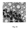
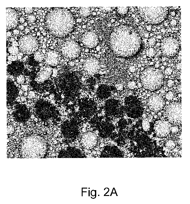
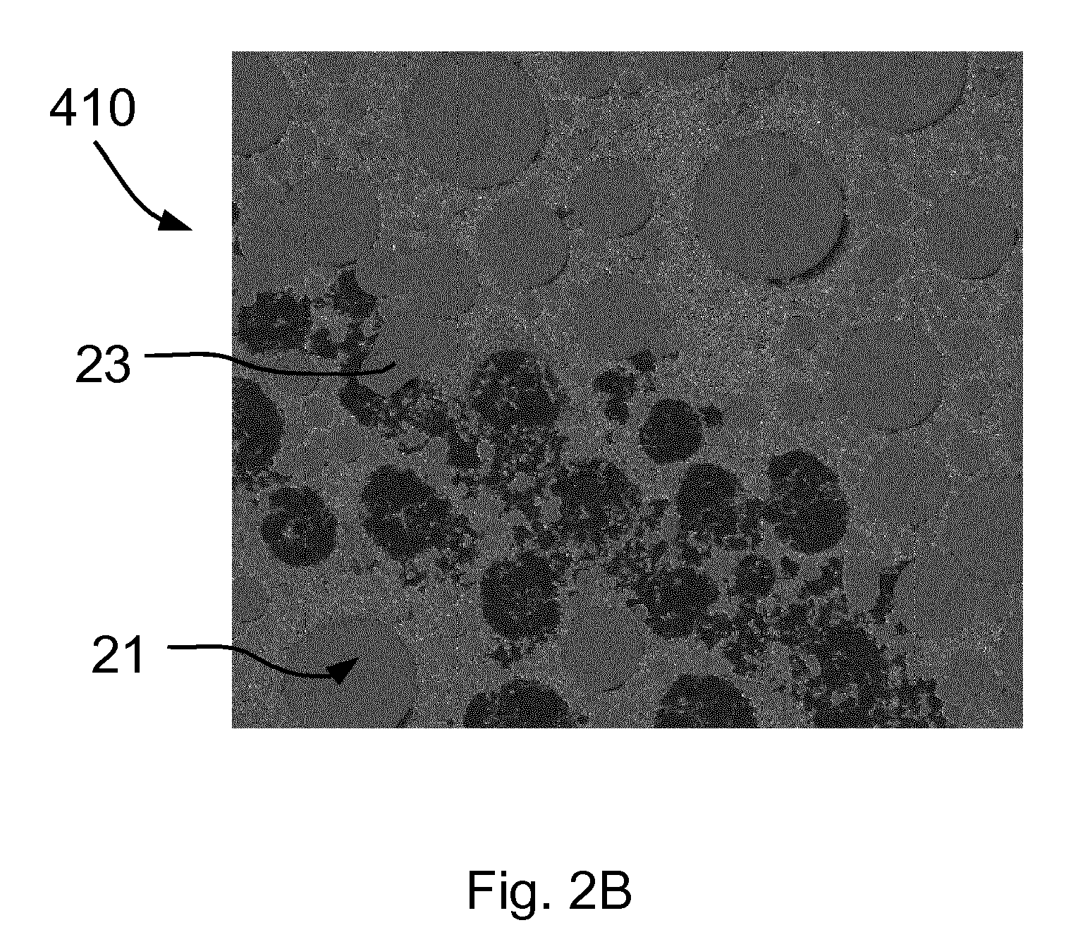
- FIGS. 2A , 2B and 2C illustrate the effect of a particular embodiment of the current invention as enacted using a set-up as set forth in Embodiment 1 above.
- the figures all show part of the same sample 410, which in this case comprises tin (Sn) droplets sputtered on carbon (C), imaged using BS electrons in a SEM on the basis of the following imaging parameters:
- Figure 2A shows a conventional BS electron image of part of the employed sample 410, being an averaged image derived from the set ⁇ I j ⁇ .
- this image is convoluted/unresolved as regards the energies ( E ) and numbers ( N ) of BS electrons triggering the detection events used to assemble the image.
- the image in Figure 2A can be deconvolved/resolved into a pair of separate maps.
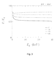
- Figure 3 graphically illustrates how the energy of BS electrons emitted from a test sample depends on the elemental constitution of that sample.
- the graph plots detected BS electron energy E (normalized to the landing energy E o of the input beam) as a function of said landing energy E o , for test samples comprising pure Au, Cu, Si and C.
- the fact that the plotted E -curves are clearly separated from one another over most of their extent (above about E o ⁇ 1 keV) illustrates the type of composition-dependent contrast that underlies the concept of an E-map as referred to above.
Landscapes
- Chemical & Material Sciences (AREA)
- Analytical Chemistry (AREA)
- Engineering & Computer Science (AREA)
- Computer Vision & Pattern Recognition (AREA)
- Physics & Mathematics (AREA)
- Health & Medical Sciences (AREA)
- Life Sciences & Earth Sciences (AREA)
- Biochemistry (AREA)
- General Health & Medical Sciences (AREA)
- General Physics & Mathematics (AREA)
- Immunology (AREA)
- Pathology (AREA)
- Analysing Materials By The Use Of Radiation (AREA)
- Image Processing (AREA)
Abstract
- Using a detector to intercept at least a portion of the flux so as to produce a set {Ij} of pixeled images Ij of at least part of the sample, whereby the cardinality of the set {Ij} is M >1.
- For each pixel pi in each image Ij, determining the accumulated signal strength Sij, thus producing an associated set of signal strengths {Sij}.
- Using the set {Sij} to calculate the following values:
▪ An average signal strength S per pixel position i;
▪ A variance σ2 S in S per pixel position i.
- Using these values S and σ2 S to at least one map of said part of the sample, selected from the group comprising:
▪ A first map, representing variation in energy of detected electrons as a function of position.
▪ A second map, representing variation in number of detected electrons as a function of position.
- By iteratively repeating a procedure whereby an entire nth image In is captured before proceeding to capture an entire (n+1)th image In+1; or
- By iteratively repeating a procedure whereby, at an nth pixel position, a plurality M of different detector samples is collected before proceeding to an (n+1)th pixel position.
Description
- The invention relates to a method of investigating a flux of output electrons emanating from a sample in a charged-particle microscope, which flux is produced in response to irradiation of the sample by a beam of input charged particles.
- The invention additionally relates to a charged-particle microscope comprising:
- A charged-particle source, for producing an irradiating beam of charged particles.
- A sample holder, for holding a sample to be irradiated.
- A particle-optical column, for directing said beam onto said sample.
- A detector, for detecting a flux of output electrons emanating from the sample in response to said irradiation.
- As used throughout this text, the ensuing terms should be interpreted consistent with the following explanation:
- The phrase "charged particle" encompasses an electron or ion (generally a positive ion, such as a Gallium ion or Helium ion, for example, although a negative ion is also possible; the ion in question may be a charged atom or molecule). The term may also refer to a proton, for example.
- The term "microscope" refers to an apparatus that is used to create a magnified image of an object, feature or component that is generally too small to be seen in satisfactory detail with the naked human eye. In a charged-particle microscope (CPM), a beam of input charged particles is directed onto a sample using a so-called "particle-optical column", which comprises a collection of electrostatic and/or magnetic lenses that can be used to manipulate said beam, serving to provide it with a certain focus or deflection, for example, and/or to mitigate one or more aberrations therein. In certain types of CPM, a different particle-optical column may also be used to focus charged particles emanating from the sample onto a detector. In addition to imaging, a CPM may also have other functionalities, such as performing spectroscopy, examining diffractograms, performing (localized) surface modification (e.g. milling, etching, deposition), etc.
- Charged-particle microscopy is a well-known and increasingly important technique for imaging microscopic objects, particularly in the form of electron microscopy. Historically, the basic genus of electron microscope has undergone evolution into a number of well-known apparatus species, such as the Transmission Electron Microscope (TEM), Scanning Electron Microscope (SEM), and Scanning Transmission Electron Microscope (STEM), and also into various sub-species, such as so-called "dual-beam" tools (e.g. a FIB-SEM), which additionally employ a "machining" Focused Ion Beam (FIB), allowing supportive activities such as ion-beam milling or Ion-Beam-Induced Deposition (IBID), for example. In a TEM, the electron beam used to irradiate a sample will generally be of significantly higher energy than in the case of a SEM (e.g. 300 keV vs. 10 keV), so as to allow its constituent electrons to penetrate the full depth of the sample; for related reasons, a sample investigated in a TEM will also generally need to be thinner than one investigated in a SEM. In traditional electron microscopes, the imaging beam is "on" for an extended period of time during a given imaging session; however, electron microscopes are also available in which imaging occurs on the basis of a relatively short "flash" or "burst" of electrons, such an approach being of potential benefit when attempting to image moving samples or radiation-sensitive specimens, for example.
- When a charged-particle beam impinges on a sample, it generally interacts with the sample in a manner that causes different types of output radiation to emanate from the sample. Such output radiation may, for example, comprise electrons (including so-called Secondary Electrons and/or Backscattered Electrons), visible/infrared/ultraviolet light (fluorescence and cathodoluminescence) and X-rays. Of these radiation types:
- Electrons may, for example, be detected using a photo-multiplier tube (PMT) in conjunction with a scintillator. It should be noted in this context that the employed PMT may be based on an evacuated vitreous tube containing dynodes, or may instead employ a solid-state semiconductor-based detection element (as in the case of a so-called Multi-Pixel Photon Counter (MPPC®) / Solid State Photo-Multiplier (SSPM)). One may also, for example, use a photodiode cell, Charge-Coupled Device (CCD) or Complementary Metal Oxide Semiconductor (CMOS) detector, possibly supplemented by a scintillator.
- Photonic radiation in the form of visible/infrared/ultraviolet light can, for example, be detected using a PMT (without scintillator), a photodiode cell, a CCD or a CMOS detector.
- X-rays tend to be more difficult to detect. Detectors for this purpose are typically relatively expensive and slow, and generally offer a relatively limited field of view. However, X-ray detection is conventionally of great use in performing compositional/elemental analyses of samples, such as in the case of so-called EDS (Energy Dispersive X-ray Spectroscopy) detectors, for example
- http://en.wikipedia.org/wiki/Secondary_electrons
- http://en.wikipedia.org/wiki/Scanning electron microscope (sections concerning detection of Secondary and Backscattered electrons).
- http://en.wikipedia.org/wiki/Transmission electron microscopy
- The imaging of a sample using an electron flux emanating therefrom exploits the fact that, for given input beam parameters, the number and/or energy of electrons emerging from a given point on the sample will be influenced by the structure and/or composition of the sample at the point in question. Recording and visually rendering the flux value as a function of position on the sample can thus be used to create an "image" of the sample (or at least a part thereof). A problem with this procedure, however, is that the electron generation and detection processes involved are intrinsically "convoluted", inter alia as a result of the following:
- The electron generation process is statistical in nature, in that there is generally temporal variability in the numbers and/or energies of electrons emanating from a given point on the sample (for a given stimulation using an input beam).
- Conventional electron detection in a CPM involves the registering of cumulative electron energy during a given temporal window (after which a refresh/reset will occur). In this context, a typical detector will, for example, not be able to discern whether a registered cumulative energy was due to a low flux of high-energy electrons, or a high flux of low-energy electrons, or a hybrid/mixed scenario.
- It is an object of the invention to address the issues raised above. More specifically, it is an object of the invention to provide a method as set forth in the opening paragraph above, whereby an acquired electron image of the sample can be (at least partially) deconvolved. In particular, it is an object of the current invention that such a method should allow more specific electron imaging of a sample to be performed..
- These and other objects are achieved in a method as set forth in the opening paragraph above, which method is characterized in that it comprises the following steps:
- Using a detector to intercept at least a portion of the flux so as to produce a set {Ij} of pixeled images Ij of at least part of the sample, whereby the cardinality of the set {Ij} is M > 1.
- For each pixel pi in each image Ij, determining the accumulated signal strength Sij, thus producing an associated set of signal strengths {Sij}.
- Using the set {Sij} to calculate the following values:
- ▪ An average signal strength S per pixel position i;
- ▪ A variance σ2 S in S per pixel position i.
- Using these values S and σ2 S to produce at least one map of said part of the sample, selected from the group comprising:
- ▪ A first map, representing variation in energy of detected electrons as a function of position;
- ▪ A second map, representing variation in number of detected electrons as a function of position.
- An image Ij is considered to be "pixeled" if it can be sub-divided into a plurality of (real or imaginary) constitutive sub-regions - which may or may not correspond to detection pixels in a case where a pixelated detector is used to produce the image in question.
- Each/either of said first and second maps is produced using both of the values of S and σ2 S.
- The current invention exploits the insight that the statistical nature of the electron emission process set forth above can be exploited advantageously rather than being regarded as a nuisance. The inventors took the unusual step of recording multiple images of a sample - not for conventional noise reduction purposes, but to act purely as a basis to perform statistical analysis. This might generally be considered as counter-productive, e.g. in terms of throughput penalty and generally increased radiation dose to the sample.
However, by examining these various images on a pixel-by-pixel basis, and mathematically processing them, the fact that the inventors had recorded multiple (temporally disparate) images allowed statistical averages/means (S) and variances (σ2 S) per pixel to be distilled from the data. This effectively amounted to a deconvolution process, whereby two different parameters could be separated from one another in data that was initially "muddled" in nature. By considering the electron production/imaging process in more detail, the inventors realized that the distilled values of S and σ2 S scaled in different ways with the energy (E) and number (N) of electrons arriving at the detector, thus allowing a separate "E-map" and "N-map" of the sample to be produced. This can, for example, be explained as follows: - The quantity S demonstrates functional behavior that can be expressed as follows:

whereby:- ▪ No describes the average number of charged particles (e.g. electrons) in the input beam, and demonstrates variations according to a Poisson process.
- ▪ η describes the probability of detecting a signal at the employed detector, and demonstrates variations according to a binomial process.
- ▪ E describes the average energy of the detected electrons resulting from the impact of a single input particle, and varies according to an unknown random process.
- The combination of said Poisson and binomial processes results in a Poisson process with an average value N = No η, being a measure of the number of detected electrons per input particle. One can thus write:

- The variance σ2 S in S demonstrates functional behavior that can be expressed as follows:

- Combining expressions (1 a) and (2), it follows that:


where f and g are functions. For example:

- Since these values are calculated per pixel, a plot of their values per pixel respectively renders:
- A first map (E-map) of the sample, which essentially reveals only compositional variation across the (imaged part of the) sample (e.g. regions comprising different contaminants/dopants, general transitions from one material to another, etc.);
- A second map (N-map) of the sample, which inter alia reveals topographical variation across the (imaged part of the) sample (e.g. edges, bumps and hollows, trenches and ridges, granulation, cracking, etc.).
- http://en.wikipedia.org/wiki/Average
- http://en.wikipedia.org/wiki/Variance
- http://en.wikipedia.org/wiki/Standard_deviation
- Needless to say, the accuracy of the procedure set forth in the previous paragraph will depend inter alia on the number M of accumulated images Ij, i.e. on the cardinality M of the set {Ij}. This is a matter of choice, and the skilled artisan will be able to decide how to manage the tradeoff between greater accuracy (in the calculated values of S and σS) on the one hand, and the competing issue of throughput on the other hand. Another issue that may need to be considered is the total radiation dose delivered to the sample, and an acceptable upper limit in this regard may place a restriction on the value of M. However, the inventors have observed that, because the current invention is predominantly interested in the differences between images in the set {Ij} more than on the direct content of the images Ij themselves, there are situations in which it is possible to lower the dose per image so as to (partially) compensate for the multiplicity of images acquired - thus decreasing the cumulative radiation dose for the whole image set {Ij}. Moreover, in calculating values of S and σ2 S from analysis of the set {Sij}, intelligent algorithms can be used to produce more refined values of S and σ2 S from smaller data sets, e.g. by extrapolating/interpolating data from a cluster of ancillary (neighboring) pixels adjacent to any given subject pixel; in this way, one can suffice with a smaller value of M to start off with. By way of non-limiting example, provided for general guidance purposes only, the inventors achieved satisfactory results with the current invention in the case of a sample comprising gold islands on carbon and using M in the range 50 - 300, for instance.
- For purposes of information and guidance, a supplemental elucidation of (some of) the considerations in the previous paragraph can be set forth as follows. Considering the detection of BS electrons, and taking E and N to be specified by equations (3a) and (4a), respectively, one can derive the following (somewhat simplified) expressions for the relative errors in E and N, with respective standard deviations σE and σN:


in which:

where: - As already alluded to above, No is the dose per image, η is the BS electron yield combined with the detector yield, and M is the cardinality of the set {Ij}.
- κ is the so-called Kurtosis of distribution of the measured signal in question, with κ ∼ 1/N (e.g. κ ≈ 22/N for carbon and κ ≈ 2/N for gold).
- http://en.wikipedia.org/wiki/Kurtosis
- It should be noted that, according to the current invention, there are different manners in which the set {Ij} can be produced. For example:
- (i) In one approach, the set {Ij} is produced by iteratively repeating (with a total of M iterations) a procedure in which an entire nth image In is captured before proceeding to capture an entire (n+1)th image In+1. In this case, the set {Ij} is basically a stack of M individual pre-assembled images Ij.
Such an approach can, for example, be enacted using detection scheme (a) or (b) below. - (ii) In an alternative approach, the set {Ij} is produced by iteratively repeating a procedure in which, at an nth pixel position, a plurality M of different detector samples is collected before proceeding to an (n+1)th pixel position. In this case, the set {Ij} is basically assembled by juxtaposing pixel stacks on a two-dimensional floor area - somewhat like mini-skyscrapers with M floors arranged side-by-side; a given image In is then the cumulative floor area made up of all nth floors of the individual skyscrapers in question. So, in this case, individual images Ij can be regarded as post-assembled rather than pre-assembled. In this scenario, whether or not one actually takes the trouble to explicitly "resolve" (assemble) individual images Ij out of the "unresolved" set {Ij} is not of particular relevance to the current invention: the main object is to accrue the dataset {Sij} and the associated values of S and σ2 S via the set {Ij} (resolved or not). Such an approach can, for example, be enacted using detection scheme (a) below.
- (iii) If desired, one can conceive various hybrids/mixes of approaches (i) and (ii).
- (a) Scan-based detection, whereby:
- The detector is a single-segment detector (for example);
- An image is produced by scanning the beam of input charged particles relative to the sample.
- (b) "Full-field" detection. Here, the full sample (or a relatively large area thereof) is irradiated using a relatively broad beam of input charged particles, and a pixelated detector (such as a CCD or CMOS array, for example) is used to capture electrons emanating from the whole irradiated zone on the sample, leading to outright formation of a two-dimensional image. Such a procedure is commonly employed in a TEM, for example.
- (c) If desired, one can conceive various hybrids/mixes of schemes (a) and (b).
- In a particular embodiment of the current invention, the flux of output electrons comprises BS electrons. BS electrons lend themselves particularly to application of the statistical processing approach of the present invention because they tend to have a relatively large energy spread. Moreover, they tend to yield better detection contrast than secondary electrons, for example. In addition, the relatively high energy of BS electrons (as compared to secondary electrons) makes them relatively easy to detect vis-à-vis the typical detection threshold of commonly employed detectors.
- Another embodiment of the present invention is characterized in that the employed detector is a solid state detector. Solid state detectors have certain advantages over more conventional dynode-based PMTs. For example, the former have good linearity in detected energy, and tend to be (much) smaller and cheaper than the latter. In addition, the former can, if desired, be relatively easily embodied as integrated pixelated detectors, which is not possible for the latter. In the context of such solid state detectors, the inventors have achieved particularly good results for the current invention with detectors that employ boron-doped detection cells (such as a delta-doped boron p + n photodiode, for example). Such boron-doped detectors are advantageous inter alia in that they are relatively sensitive and highly linear, even for electron energies as low as ca. 200eV. As regards the basic structure and operation of such detectors, more information can, for example, be gleaned from the following technical journal links:
- http://ectm.et.tudelft.nl/publications pdf/document1249.pdf
- http://www.electrochem.ora/dl/ma/202/pdfs/0672.PDF
- The invention will now be elucidated in more detail on the basis of exemplary embodiments and the accompanying schematic drawings, in which:
-
Figure 1 renders an elevational view of a charged-particle microscope that lends itself to use with the current invention. -
Figure 2A shows a conventional BS electron image of part of a tin-on-carbon sample. -
Figure 2B shows the subject ofFigure 2A , but now rendered as a first-type map (E-map) using the current invention, and revealing compositional information. -
Figure 2C also shows the subject ofFigure 2A , but now rendered as a second-type map (N-map) using the current invention, and inter alia revealing (mainly) topographical information. -
Figure 3 graphically illustrates how the energy of BS electrons emitted from a test sample depends on the elemental constitution of that sample. - In the Figures, where pertinent, corresponding parts are indicated using corresponding reference symbols. It should be noted that, in general, the Figures are not to scale.
-
Figure 1 is a highly schematic depiction of a charged-particle microscope 400, which, in this case, is a SEM. Themicroscope 400 comprises a particle-optical column 402, which produces abeam 404 of input charged particles (in this case, an electron beam). The particle-optical column 402 is mounted on avacuum chamber 406, which comprises a sample holder /stage 408 for holding asample 410. Thevacuum chamber 406 is evacuated using vacuum pumps (not depicted). With the aid ofvoltage source 422, thesample holder 408, or at least thesample 410, may, if desired, be biased (floated) to an electrical potential with respect to ground. - The particle-
optical column 402 comprises an electron source 412 (such as a Schottky gun),lenses electron beam 404 onto thesample 410, and a deflection unit 418 (to perform beam steering / scanning of the beam 404). Theapparatus 400 further comprises a controller /computer processing apparatus 424 for controlling inter alia thedeflection unit 418,lenses detectors detectors display unit 426. - The
detectors sample 410 in response to irradiation by theinput beam 404. In the apparatus depicted here, the following detector choices have been made: -
Detector 100 is a segmented electron detector. Such a detector can, for example, be used to investigate the angular dependence of a flux of output (secondary) electrons emerging from thesample 410. -
Detector 420 is a boron-doped solid state detector that is used to detect (at least a portion of) a flux of output BS electrons emanating from thesample 410. - By scanning the
input beam 404 over thesample 410, output radiation - comprising, for example, X-rays, infrared/visible/ultraviolet light, secondary electrons and backscattered (BS) electrons - emanates from thesample 410. As such output radiation is position-sensitive (due to said scanning motion), the information obtained from thedetectors detector 420 to be used to produce a BS electron image of (part of) thesample 410, which image is basically a map of an output ofdetector 420 as a function of scan-path position on thesample 410. - The signals from the
detectors controller 424, and displayed ondisplay unit 426. Such processing may include operations such as combining, integrating, subtracting, false colouring, edge enhancing, and other processing known to the skilled artisan. In addition, automated recognition processes (e.g. as used for particle analysis) may be included in such processing. In the specific context of the current invention, the controller 424 - and/or a dedicated separate processing unit (not shown) - can be used to perform the following actions: - Using
detector 420 to produce a set {Ij} of pixeled BS electron images Ij of at least part of thesample 410, whereby the cardinality of the set {Ij} is M > 1. As set forth above, this may, for example be done:- ▪ On a pixel-by-pixel basis, whereby M samples of the BS electron flux are measured in succession at a given position on the
sample 410 before moving thebeam 404 onto a next position on thesample 410; or - ▪ On an image-by-image basis, whereby an entire scan of (said part of) the
sample 410 is made bybeam 404, leading to creation of a whole image Ij, and this procedure is performed a total of M times in succession.
- ▪ On a pixel-by-pixel basis, whereby M samples of the BS electron flux are measured in succession at a given position on the
- For each pixel pi in each image Ij, determining the accumulated signal strength Sij, thus producing an associated set of signal strengths {Sij}.
- Using the set {Sij} to calculate the following values:
- ▪ An average signal strength S per pixel position i;
- ▪ A variance σ2 S in S per pixel position i.
- Using these values S and σ2 S (as input to equations (3a) and (4a) above, for example), to produce one or both of the following maps of said part of the sample 410:
- ▪ A first map, representing variation in energy (E) of detected BS electrons as a function of position on the
sample 410. - ▪ A second map, representing variation in number (N) of detected BS electrons as a function of position on the
sample 410.
- ▪ A first map, representing variation in energy (E) of detected BS electrons as a function of position on the
- It should be noted that many refinements and alternatives of such a set-up will be known to the skilled artisan, including, but not limited to:
- The use of dual beams - for example an
electron beam 404 for imaging and an ion beam for machining (or, in some cases, imaging) thesample 410; - The use of a controlled environment at the sample 410 - for example, maintaining a pressure of several mbar (as used in a so-called Environmental SEM) or by admitting gases, such as etching or precursor gases,
- For more information on some of the topics alluded to above, reference is made to the following Wikipedia links:
- http://en.wikipedia.org/wiki/Field emission gun
- http://en.wikipedia.org/wiki/Electron optics
-
Figures 2A ,2B and 2C illustrate the effect of a particular embodiment of the current invention as enacted using a set-up as set forth in Embodiment 1 above. The figures all show part of thesame sample 410, which in this case comprises tin (Sn) droplets sputtered on carbon (C), imaged using BS electrons in a SEM on the basis of the following imaging parameters: - Landing energy of input electron beam 404: 5 keV.
- Beam current of input electron beam 404: 170 pA.
- Dwelling time τ = 6 µs (= time to compile a single pixel of the BS electron image).
- M (cardinality of measured image set {Ij}) = 300, i.e. 300 different BS electron measurement samples were recorded per pixel position, or 300 full BS electron images Ij were serially acquired.
-
Figure 2A shows a conventional BS electron image of part of the employedsample 410, being an averaged image derived from the set {Ij}. As already explained above, this image is convoluted/unresolved as regards the energies (E) and numbers (N) of BS electrons triggering the detection events used to assemble the image. However, by processing the set {Ij} to produce a set {Sij} as set forth above in accordance with the current invention, the image inFigure 2A can be deconvolved/resolved into a pair of separate maps. In this context: -
Figure 2B shows the subject ofFigure 2A , but now rendered using the current invention as a first-type map (E-map) as alluded to above, and revealing compositional information of the employedsample 410. The contrast-to-noise ratio (CNR) for the depicted map is ca. 3.56. -
Figure 2C also shows the subject ofFigure 2A , but now rendered using the current invention as a second-type map (N-map) as alluded to above, and revealing inter alia (mostly) topographical information of the employedsample 410. - An oval "dent" 21 visible in
Figure 2C is absent fromFigure 2B . - A
droplet 23 that appears to be substantially wrinkled/broken inFigure 2C appears substantially featureless inFigure 2B . -
Figure 3 graphically illustrates how the energy of BS electrons emitted from a test sample depends on the elemental constitution of that sample. The graph plots detected BS electron energy E (normalized to the landing energy Eo of the input beam) as a function of said landing energy Eo , for test samples comprising pure Au, Cu, Si and C. The fact that the plotted E-curves are clearly separated from one another over most of their extent (above about Eo ≈ 1 keV) illustrates the type of composition-dependent contrast that underlies the concept of an E-map as referred to above.
The skilled artisan will be well able to quantify S and σ2 S from analysis of the set {Sij}, e.g. using relatively straightforward software to automatically analyze the data {Sij} and determine attendant averaged amplitudes and spreads per pixel. In so doing, he has the freedom to choose from various estimators for the required average/mean and variance; for example, in the case of the quantify S, the employed average/mean may be a simple arithmetic average (sum of values divided by number of values), or another type of estimator. Similarly, relatively simple software will be able to automatically perform calculations such as those set forth in equations (3a) and (4a) above, for example. The software in question may be executed with the aid of a controller, such as an electronic microprocessor, which may also be programmed/invoked to automatically collect the dataset {Ij}, render the first and second maps on a display device, etc. Inter alia in the context of the elucidation just given, reference is made to the following explanatory Wikipedia links, for general information purposes:
Inter alia in the context of the elucidation just given, reference is made to the following explanatory Wikipedia link, for general information purposes:
Claims (9)
- A method of investigating a flux of output electrons emanating from a sample in a charged-particle microscope, which flux is produced in response to irradiation of the sample by a beam of input charged particles, characterized in that the method comprises the following steps:- Using a detector to intercept at least a portion of the flux so as to produce a set {Ij} of pixeled images Ij of at least part of the sample, whereby the cardinality of the set {Ij} is M > 1.- For each pixel pi in each image Ij, determining the accumulated signal strength Sij, thus producing an associated set of signal strengths {Sij}.- Using the set {Sij} to calculate the following values:▪ An average signal strength S per pixel position i;▪ A variance σ2 S in S per pixel position i.- Using these values S and σ2 S to produce at least one map of said part of the sample, selected from the group comprising:▪ A first map, representing variation in energy of detected electrons as a function of position.▪ A second map, representing variation in number of detected electrons as a function of position.
- A method as claimed in claim 1, wherein the set {Ij} is produced by iteratively repeating a procedure whereby an entire nth image In is captured before proceeding to capture an entire (n+1)th image In+1.
- A method as claimed in claim 1, wherein the set {Ij} is produced by iteratively repeating a procedure whereby, at an nth pixel position, a plurality M of different detector samples is collected before proceeding to an (n+1)th pixel position.
- A method according to any of claims 1-3, wherein said flux of output electrons comprises backscattered electrons.
- A method according to any of claims 1-4, wherein said detector is a solid state detector.
- A method according to claim 5, wherein said solid state detector comprises at least one boron-doped diode detection cell.
- A method according to any of claims 1-6, wherein said first map is produced with the aid of a functional dependence E ∼ σS 2 / S per pixel position i.
- A method according to any of claims 1-7, wherein said second map is produced with the aid of a functional dependence N ∼ S2 / σS 2 per pixel position i.
- A charged-particle microscope comprising:- A charged-particle source, for producing an irradiating beam of charged particles.- A sample holder, for holding a sample to be irradiated.- A particle-optical column, for directing said beam onto said sample.- A detector, for detecting a flux of output electrons emanating from the sample in response to said irradiation,characterized in that the charged-particle microscope further comprises a controller for performing the following actions:- Using said detector to produce a set {Ij} of pixeled images Ij of at least part of the sample, whereby the cardinality of the set {Ij} is M > 1.- For each pixel pi in each image Ij, determining the accumulated signal strength Sij, thus producing an associated set of signal strengths {Sij}.- Using the set {Sij} to calculate the following values:▪ An average signal strength S per pixel position i;▪ A variance σ2 S in S per pixel position i.- Using these values S and σ2 S to produce at least one map of said part of the sample, selected from the group comprising:▪ A first map, representing variation in energy of detected electrons as a function of position.▪ A second map, representing variation in number of detected electrons as a function of position.
Priority Applications (1)
| Application Number | Priority Date | Filing Date | Title |
|---|---|---|---|
| EP14195296.0A EP2879157B1 (en) | 2013-12-02 | 2014-11-28 | Charged-particle microscopy with enhanced electron detection |
Applications Claiming Priority (2)
| Application Number | Priority Date | Filing Date | Title |
|---|---|---|---|
| EP13195289.7A EP2879156A1 (en) | 2013-12-02 | 2013-12-02 | Charged-particle microscopy with enhanced electron detection |
| EP14195296.0A EP2879157B1 (en) | 2013-12-02 | 2014-11-28 | Charged-particle microscopy with enhanced electron detection |
Publications (2)
| Publication Number | Publication Date |
|---|---|
| EP2879157A1 true EP2879157A1 (en) | 2015-06-03 |
| EP2879157B1 EP2879157B1 (en) | 2016-01-13 |
Family
ID=49674236
Family Applications (2)
| Application Number | Title | Priority Date | Filing Date |
|---|---|---|---|
| EP13195289.7A Withdrawn EP2879156A1 (en) | 2013-12-02 | 2013-12-02 | Charged-particle microscopy with enhanced electron detection |
| EP14195296.0A Active EP2879157B1 (en) | 2013-12-02 | 2014-11-28 | Charged-particle microscopy with enhanced electron detection |
Family Applications Before (1)
| Application Number | Title | Priority Date | Filing Date |
|---|---|---|---|
| EP13195289.7A Withdrawn EP2879156A1 (en) | 2013-12-02 | 2013-12-02 | Charged-particle microscopy with enhanced electron detection |
Country Status (4)
| Country | Link |
|---|---|
| US (1) | US9208993B2 (en) |
| EP (2) | EP2879156A1 (en) |
| JP (1) | JP6294216B2 (en) |
| CN (1) | CN104681382B (en) |
Families Citing this family (8)
| Publication number | Priority date | Publication date | Assignee | Title |
|---|---|---|---|---|
| EP3040714A1 (en) | 2014-12-30 | 2016-07-06 | Fei Company | Charged Particle Microscope with improved spectroscopic functionality |
| EP3106862B1 (en) | 2015-06-18 | 2019-01-16 | FEI Company | Method of ptychographic imaging |
| US10122946B2 (en) | 2015-11-11 | 2018-11-06 | Fei Company | Method for detecting particulate radiation |
| US10685759B2 (en) * | 2017-01-16 | 2020-06-16 | Fei Company | Statistical analysis in X-ray imaging |
| JP6796616B2 (en) * | 2018-05-24 | 2020-12-09 | 日本電子株式会社 | Charged particle beam device and image acquisition method |
| JP7072457B2 (en) * | 2018-07-12 | 2022-05-20 | 株式会社堀場製作所 | Sample analyzer, electron microscope, and condensing mirror unit |
| EP3726206B1 (en) * | 2019-03-26 | 2022-11-02 | FEI Company | Methods and systems for inclusion analysis |
| US10928336B1 (en) * | 2019-07-29 | 2021-02-23 | Applied Materials Israel Ltd. | X-ray based evaluation of a status of a structure of a substrate |
Citations (7)
| Publication number | Priority date | Publication date | Assignee | Title |
|---|---|---|---|---|
| WO2000070646A1 (en) * | 1999-05-14 | 2000-11-23 | Applied Materials, Inc. | Secondary electron spectroscopy method and system |
| WO2003003402A1 (en) * | 2001-06-29 | 2003-01-09 | Kla-Tencor Corporation | Energy filter multiplexing |
| JP2005134181A (en) * | 2003-10-29 | 2005-05-26 | Jeol Ltd | Data processing method and analyzing apparatus |
| WO2006109564A1 (en) * | 2005-04-11 | 2006-10-19 | Shimadzu Corporation | Data processing method for scanning beam device |
| WO2009079195A1 (en) * | 2007-12-17 | 2009-06-25 | Alis Corporation | Ion beam imaging |
| US20130054153A1 (en) * | 2011-03-23 | 2013-02-28 | Tescan, A.S. | Method and apparatus for material analysis by a focused electron beam using characteristic x-rays and back-scattered electrons |
| EP2665083A2 (en) * | 2012-05-17 | 2013-11-20 | Fei Company | Scanning microscope having an adaptive scan |
Family Cites Families (7)
| Publication number | Priority date | Publication date | Assignee | Title |
|---|---|---|---|---|
| JP2004214060A (en) * | 2003-01-06 | 2004-07-29 | Hitachi High-Technologies Corp | Scanning electron microscope and sample observation method using the same |
| CN1553466A (en) | 2003-12-19 | 2004-12-08 | �й���ѧԺ�Ϻ���ѧ���ܻ�е�о��� | High-power composite function quartz glass tube pulse xenon lamp |
| US7601045B2 (en) | 2004-07-16 | 2009-10-13 | Tangle, Inc. | Therapeutic hand toys |
| JP2007220317A (en) * | 2006-02-14 | 2007-08-30 | Jeol Ltd | Electron beam inspection method and apparatus |
| TWI435361B (en) * | 2007-04-16 | 2014-04-21 | Ebara Corp | Electronic ray device and method for observing a test piece using such electronic ray device |
| JP5065516B2 (en) * | 2010-08-04 | 2012-11-07 | エフ イー アイ カンパニ | Reduction of backscattering in thin electron detectors. |
| JP5995773B2 (en) * | 2012-04-05 | 2016-09-21 | エフ イー アイ カンパニFei Company | Inspection method and charged particle microscope |
-
2013
- 2013-12-02 EP EP13195289.7A patent/EP2879156A1/en not_active Withdrawn
-
2014
- 2014-11-28 EP EP14195296.0A patent/EP2879157B1/en active Active
- 2014-12-01 JP JP2014243188A patent/JP6294216B2/en active Active
- 2014-12-02 US US14/558,334 patent/US9208993B2/en active Active
- 2014-12-02 CN CN201410718566.8A patent/CN104681382B/en active Active
Patent Citations (7)
| Publication number | Priority date | Publication date | Assignee | Title |
|---|---|---|---|---|
| WO2000070646A1 (en) * | 1999-05-14 | 2000-11-23 | Applied Materials, Inc. | Secondary electron spectroscopy method and system |
| WO2003003402A1 (en) * | 2001-06-29 | 2003-01-09 | Kla-Tencor Corporation | Energy filter multiplexing |
| JP2005134181A (en) * | 2003-10-29 | 2005-05-26 | Jeol Ltd | Data processing method and analyzing apparatus |
| WO2006109564A1 (en) * | 2005-04-11 | 2006-10-19 | Shimadzu Corporation | Data processing method for scanning beam device |
| WO2009079195A1 (en) * | 2007-12-17 | 2009-06-25 | Alis Corporation | Ion beam imaging |
| US20130054153A1 (en) * | 2011-03-23 | 2013-02-28 | Tescan, A.S. | Method and apparatus for material analysis by a focused electron beam using characteristic x-rays and back-scattered electrons |
| EP2665083A2 (en) * | 2012-05-17 | 2013-11-20 | Fei Company | Scanning microscope having an adaptive scan |
Non-Patent Citations (1)
| Title |
|---|
| RAPHAEL SZNITMAN ET AL: "Efficient Scanning for EM Based Target Localization", 1 October 2012, MEDICAL IMAGE COMPUTING AND COMPUTER-ASSISTED INTERVENTION MICCAI 2012, SPRINGER BERLIN HEIDELBERG, BERLIN, HEIDELBERG, PAGE(S) 337 - 344, ISBN: 978-3-642-33453-5, XP047018334 * |
Also Published As
| Publication number | Publication date |
|---|---|
| CN104681382A (en) | 2015-06-03 |
| JP6294216B2 (en) | 2018-03-14 |
| EP2879156A1 (en) | 2015-06-03 |
| CN104681382B (en) | 2017-07-07 |
| US9208993B2 (en) | 2015-12-08 |
| US20150155131A1 (en) | 2015-06-04 |
| EP2879157B1 (en) | 2016-01-13 |
| JP2015106565A (en) | 2015-06-08 |
Similar Documents
| Publication | Publication Date | Title |
|---|---|---|
| EP2879157B1 (en) | Charged-particle microscopy with enhanced electron detection | |
| EP2963673B1 (en) | Computational scanning microscopy with improved resolution | |
| US9618460B2 (en) | Method of performing tomographic imaging of a sample in a charged-particle microscope | |
| EP3477289A1 (en) | X-ray spectroscopy in a charged particle microscope | |
| EP2525386B1 (en) | Charged-particle microscopy with occlusion detection | |
| EP2557587B1 (en) | Charged-particle microscope providing depth-resolved imagery | |
| US20140175279A1 (en) | Charged particle beam apparatus | |
| JP5050705B2 (en) | Mass spectrometer | |
| US9805910B1 (en) | Automated SEM nanoprobe tool | |
| WO2009035841A1 (en) | Determining dopant information by use of a helium ion microscope | |
| EP3240013B1 (en) | Three-dimensional imaging in charged-particle microscopy | |
| JP2013243128A (en) | Scanning microscope having adaptive scanning | |
| JP2014021124A (en) | Spectroscopy using merged spectral data | |
| JP7068811B2 (en) | Statistical analysis of X-ray imaging | |
| EP2660845A1 (en) | Charged-particle microscopy with image stitching | |
| EP2698805A1 (en) | Method of performing EDX in a charged-particle microscope | |
| CN120177530A (en) | System and method for analyzing a sample using a charged particle beam and an active pixel control sensor | |
| Tarolli et al. | High resolution isotopic analysis of U-bearing particles via fusion of SIMS and EDS images | |
| Andersen et al. | Time-of-flight scanning transmission ion microscopy with high energy resolution in the low keV range | |
| Tan et al. | Study of Silicon thickness for electron transparency | |
| Hempel et al. | Spatially-Resolved Elemental Analysis |
Legal Events
| Date | Code | Title | Description |
|---|---|---|---|
| PUAI | Public reference made under article 153(3) epc to a published international application that has entered the european phase |
Free format text: ORIGINAL CODE: 0009012 |
|
| 17P | Request for examination filed |
Effective date: 20141128 |
|
| AK | Designated contracting states |
Kind code of ref document: A1 Designated state(s): AL AT BE BG CH CY CZ DE DK EE ES FI FR GB GR HR HU IE IS IT LI LT LU LV MC MK MT NL NO PL PT RO RS SE SI SK SM TR |
|
| AX | Request for extension of the european patent |
Extension state: BA ME |
|
| R17P | Request for examination filed (corrected) |
Effective date: 20150626 |
|
| RBV | Designated contracting states (corrected) |
Designated state(s): AL AT BE BG CH CY CZ DE DK EE ES FI FR GB GR HR HU IE IS IT LI LT LU LV MC MK MT NL NO PL PT RO RS SE SI SK SM TR |
|
| GRAP | Despatch of communication of intention to grant a patent |
Free format text: ORIGINAL CODE: EPIDOSNIGR1 |
|
| RIC1 | Information provided on ipc code assigned before grant |
Ipc: G01N 23/225 20060101ALI20150825BHEP Ipc: H01J 37/28 20060101ALI20150825BHEP Ipc: H01J 37/22 20060101AFI20150825BHEP |
|
| INTG | Intention to grant announced |
Effective date: 20150917 |
|
| GRAS | Grant fee paid |
Free format text: ORIGINAL CODE: EPIDOSNIGR3 |
|
| GRAA | (expected) grant |
Free format text: ORIGINAL CODE: 0009210 |
|
| AK | Designated contracting states |
Kind code of ref document: B1 Designated state(s): AL AT BE BG CH CY CZ DE DK EE ES FI FR GB GR HR HU IE IS IT LI LT LU LV MC MK MT NL NO PL PT RO RS SE SI SK SM TR |
|
| REG | Reference to a national code |
Ref country code: GB Ref legal event code: FG4D |
|
| REG | Reference to a national code |
Ref country code: CH Ref legal event code: EP |
|
| REG | Reference to a national code |
Ref country code: IE Ref legal event code: FG4D |
|
| REG | Reference to a national code |
Ref country code: AT Ref legal event code: REF Ref document number: 771009 Country of ref document: AT Kind code of ref document: T Effective date: 20160215 |
|
| REG | Reference to a national code |
Ref country code: DE Ref legal event code: R096 Ref document number: 602014000738 Country of ref document: DE |
|
| REG | Reference to a national code |
Ref country code: LT Ref legal event code: MG4D |
|
| REG | Reference to a national code |
Ref country code: NL Ref legal event code: MP Effective date: 20160113 |
|
| REG | Reference to a national code |
Ref country code: AT Ref legal event code: MK05 Ref document number: 771009 Country of ref document: AT Kind code of ref document: T Effective date: 20160113 |
|
| PG25 | Lapsed in a contracting state [announced via postgrant information from national office to epo] |
Ref country code: NL Free format text: LAPSE BECAUSE OF FAILURE TO SUBMIT A TRANSLATION OF THE DESCRIPTION OR TO PAY THE FEE WITHIN THE PRESCRIBED TIME-LIMIT Effective date: 20160113 |
|
| PG25 | Lapsed in a contracting state [announced via postgrant information from national office to epo] |
Ref country code: GR Free format text: LAPSE BECAUSE OF FAILURE TO SUBMIT A TRANSLATION OF THE DESCRIPTION OR TO PAY THE FEE WITHIN THE PRESCRIBED TIME-LIMIT Effective date: 20160414 Ref country code: HR Free format text: LAPSE BECAUSE OF FAILURE TO SUBMIT A TRANSLATION OF THE DESCRIPTION OR TO PAY THE FEE WITHIN THE PRESCRIBED TIME-LIMIT Effective date: 20160113 Ref country code: IT Free format text: LAPSE BECAUSE OF FAILURE TO SUBMIT A TRANSLATION OF THE DESCRIPTION OR TO PAY THE FEE WITHIN THE PRESCRIBED TIME-LIMIT Effective date: 20160113 Ref country code: ES Free format text: LAPSE BECAUSE OF FAILURE TO SUBMIT A TRANSLATION OF THE DESCRIPTION OR TO PAY THE FEE WITHIN THE PRESCRIBED TIME-LIMIT Effective date: 20160113 Ref country code: FI Free format text: LAPSE BECAUSE OF FAILURE TO SUBMIT A TRANSLATION OF THE DESCRIPTION OR TO PAY THE FEE WITHIN THE PRESCRIBED TIME-LIMIT Effective date: 20160113 Ref country code: NO Free format text: LAPSE BECAUSE OF FAILURE TO SUBMIT A TRANSLATION OF THE DESCRIPTION OR TO PAY THE FEE WITHIN THE PRESCRIBED TIME-LIMIT Effective date: 20160413 |
|
| PG25 | Lapsed in a contracting state [announced via postgrant information from national office to epo] |
Ref country code: PT Free format text: LAPSE BECAUSE OF FAILURE TO SUBMIT A TRANSLATION OF THE DESCRIPTION OR TO PAY THE FEE WITHIN THE PRESCRIBED TIME-LIMIT Effective date: 20160513 Ref country code: IS Free format text: LAPSE BECAUSE OF FAILURE TO SUBMIT A TRANSLATION OF THE DESCRIPTION OR TO PAY THE FEE WITHIN THE PRESCRIBED TIME-LIMIT Effective date: 20160513 Ref country code: RS Free format text: LAPSE BECAUSE OF FAILURE TO SUBMIT A TRANSLATION OF THE DESCRIPTION OR TO PAY THE FEE WITHIN THE PRESCRIBED TIME-LIMIT Effective date: 20160113 Ref country code: LT Free format text: LAPSE BECAUSE OF FAILURE TO SUBMIT A TRANSLATION OF THE DESCRIPTION OR TO PAY THE FEE WITHIN THE PRESCRIBED TIME-LIMIT Effective date: 20160113 Ref country code: AT Free format text: LAPSE BECAUSE OF FAILURE TO SUBMIT A TRANSLATION OF THE DESCRIPTION OR TO PAY THE FEE WITHIN THE PRESCRIBED TIME-LIMIT Effective date: 20160113 Ref country code: SE Free format text: LAPSE BECAUSE OF FAILURE TO SUBMIT A TRANSLATION OF THE DESCRIPTION OR TO PAY THE FEE WITHIN THE PRESCRIBED TIME-LIMIT Effective date: 20160113 Ref country code: LV Free format text: LAPSE BECAUSE OF FAILURE TO SUBMIT A TRANSLATION OF THE DESCRIPTION OR TO PAY THE FEE WITHIN THE PRESCRIBED TIME-LIMIT Effective date: 20160113 Ref country code: PL Free format text: LAPSE BECAUSE OF FAILURE TO SUBMIT A TRANSLATION OF THE DESCRIPTION OR TO PAY THE FEE WITHIN THE PRESCRIBED TIME-LIMIT Effective date: 20160113 |
|
| REG | Reference to a national code |
Ref country code: DE Ref legal event code: R097 Ref document number: 602014000738 Country of ref document: DE |
|
| PG25 | Lapsed in a contracting state [announced via postgrant information from national office to epo] |
Ref country code: DK Free format text: LAPSE BECAUSE OF FAILURE TO SUBMIT A TRANSLATION OF THE DESCRIPTION OR TO PAY THE FEE WITHIN THE PRESCRIBED TIME-LIMIT Effective date: 20160113 Ref country code: EE Free format text: LAPSE BECAUSE OF FAILURE TO SUBMIT A TRANSLATION OF THE DESCRIPTION OR TO PAY THE FEE WITHIN THE PRESCRIBED TIME-LIMIT Effective date: 20160113 |
|
| PLBE | No opposition filed within time limit |
Free format text: ORIGINAL CODE: 0009261 |
|
| STAA | Information on the status of an ep patent application or granted ep patent |
Free format text: STATUS: NO OPPOSITION FILED WITHIN TIME LIMIT |
|
| REG | Reference to a national code |
Ref country code: FR Ref legal event code: PLFP Year of fee payment: 3 |
|
| PG25 | Lapsed in a contracting state [announced via postgrant information from national office to epo] |
Ref country code: SM Free format text: LAPSE BECAUSE OF FAILURE TO SUBMIT A TRANSLATION OF THE DESCRIPTION OR TO PAY THE FEE WITHIN THE PRESCRIBED TIME-LIMIT Effective date: 20160113 Ref country code: SK Free format text: LAPSE BECAUSE OF FAILURE TO SUBMIT A TRANSLATION OF THE DESCRIPTION OR TO PAY THE FEE WITHIN THE PRESCRIBED TIME-LIMIT Effective date: 20160113 Ref country code: RO Free format text: LAPSE BECAUSE OF FAILURE TO SUBMIT A TRANSLATION OF THE DESCRIPTION OR TO PAY THE FEE WITHIN THE PRESCRIBED TIME-LIMIT Effective date: 20160113 Ref country code: CZ Free format text: LAPSE BECAUSE OF FAILURE TO SUBMIT A TRANSLATION OF THE DESCRIPTION OR TO PAY THE FEE WITHIN THE PRESCRIBED TIME-LIMIT Effective date: 20160113 |
|
| 26N | No opposition filed |
Effective date: 20161014 |
|
| PG25 | Lapsed in a contracting state [announced via postgrant information from national office to epo] |
Ref country code: BE Free format text: LAPSE BECAUSE OF FAILURE TO SUBMIT A TRANSLATION OF THE DESCRIPTION OR TO PAY THE FEE WITHIN THE PRESCRIBED TIME-LIMIT Effective date: 20160113 |
|
| PG25 | Lapsed in a contracting state [announced via postgrant information from national office to epo] |
Ref country code: BG Free format text: LAPSE BECAUSE OF FAILURE TO SUBMIT A TRANSLATION OF THE DESCRIPTION OR TO PAY THE FEE WITHIN THE PRESCRIBED TIME-LIMIT Effective date: 20160413 Ref country code: SI Free format text: LAPSE BECAUSE OF FAILURE TO SUBMIT A TRANSLATION OF THE DESCRIPTION OR TO PAY THE FEE WITHIN THE PRESCRIBED TIME-LIMIT Effective date: 20160113 |
|
| REG | Reference to a national code |
Ref country code: IE Ref legal event code: MM4A |
|
| PG25 | Lapsed in a contracting state [announced via postgrant information from national office to epo] |
Ref country code: LU Free format text: LAPSE BECAUSE OF NON-PAYMENT OF DUE FEES Effective date: 20161130 |
|
| REG | Reference to a national code |
Ref country code: FR Ref legal event code: PLFP Year of fee payment: 4 |
|
| PG25 | Lapsed in a contracting state [announced via postgrant information from national office to epo] |
Ref country code: IE Free format text: LAPSE BECAUSE OF NON-PAYMENT OF DUE FEES Effective date: 20161128 |
|
| PG25 | Lapsed in a contracting state [announced via postgrant information from national office to epo] |
Ref country code: HU Free format text: LAPSE BECAUSE OF FAILURE TO SUBMIT A TRANSLATION OF THE DESCRIPTION OR TO PAY THE FEE WITHIN THE PRESCRIBED TIME-LIMIT; INVALID AB INITIO Effective date: 20141128 |
|
| PG25 | Lapsed in a contracting state [announced via postgrant information from national office to epo] |
Ref country code: CY Free format text: LAPSE BECAUSE OF FAILURE TO SUBMIT A TRANSLATION OF THE DESCRIPTION OR TO PAY THE FEE WITHIN THE PRESCRIBED TIME-LIMIT Effective date: 20160113 Ref country code: MC Free format text: LAPSE BECAUSE OF FAILURE TO SUBMIT A TRANSLATION OF THE DESCRIPTION OR TO PAY THE FEE WITHIN THE PRESCRIBED TIME-LIMIT Effective date: 20160113 Ref country code: MK Free format text: LAPSE BECAUSE OF FAILURE TO SUBMIT A TRANSLATION OF THE DESCRIPTION OR TO PAY THE FEE WITHIN THE PRESCRIBED TIME-LIMIT Effective date: 20160113 |
|
| PG25 | Lapsed in a contracting state [announced via postgrant information from national office to epo] |
Ref country code: CH Free format text: LAPSE BECAUSE OF NON-PAYMENT OF DUE FEES Effective date: 20171130 Ref country code: LI Free format text: LAPSE BECAUSE OF NON-PAYMENT OF DUE FEES Effective date: 20171130 |
|
| PG25 | Lapsed in a contracting state [announced via postgrant information from national office to epo] |
Ref country code: MT Free format text: LAPSE BECAUSE OF NON-PAYMENT OF DUE FEES Effective date: 20161128 |
|
| REG | Reference to a national code |
Ref country code: FR Ref legal event code: PLFP Year of fee payment: 5 |
|
| PG25 | Lapsed in a contracting state [announced via postgrant information from national office to epo] |
Ref country code: TR Free format text: LAPSE BECAUSE OF FAILURE TO SUBMIT A TRANSLATION OF THE DESCRIPTION OR TO PAY THE FEE WITHIN THE PRESCRIBED TIME-LIMIT Effective date: 20160113 Ref country code: AL Free format text: LAPSE BECAUSE OF FAILURE TO SUBMIT A TRANSLATION OF THE DESCRIPTION OR TO PAY THE FEE WITHIN THE PRESCRIBED TIME-LIMIT Effective date: 20160113 |
|
| PGFP | Annual fee paid to national office [announced via postgrant information from national office to epo] |
Ref country code: DE Payment date: 20251010 Year of fee payment: 12 |
|
| PGFP | Annual fee paid to national office [announced via postgrant information from national office to epo] |
Ref country code: GB Payment date: 20251114 Year of fee payment: 12 |
|
| PGFP | Annual fee paid to national office [announced via postgrant information from national office to epo] |
Ref country code: FR Payment date: 20251111 Year of fee payment: 12 |