EP2879051A1 - An electronic device including a MTD used temporarily during non-volatile memory file system update - Google Patents
An electronic device including a MTD used temporarily during non-volatile memory file system update Download PDFInfo
- Publication number
- EP2879051A1 EP2879051A1 EP14194543.6A EP14194543A EP2879051A1 EP 2879051 A1 EP2879051 A1 EP 2879051A1 EP 14194543 A EP14194543 A EP 14194543A EP 2879051 A1 EP2879051 A1 EP 2879051A1
- Authority
- EP
- European Patent Office
- Prior art keywords
- ram
- electronic device
- nonvolatile storage
- kernel
- root
- Prior art date
- Legal status (The legal status is an assumption and is not a legal conclusion. Google has not performed a legal analysis and makes no representation as to the accuracy of the status listed.)
- Granted
Links
Images




Classifications
-
- G—PHYSICS
- G06—COMPUTING OR CALCULATING; COUNTING
- G06F—ELECTRIC DIGITAL DATA PROCESSING
- G06F8/00—Arrangements for software engineering
- G06F8/60—Software deployment
- G06F8/65—Updates
- G06F8/654—Updates using techniques specially adapted for alterable solid state memories, e.g. for EEPROM or flash memories
-
- G—PHYSICS
- G06—COMPUTING OR CALCULATING; COUNTING
- G06F—ELECTRIC DIGITAL DATA PROCESSING
- G06F9/00—Arrangements for program control, e.g. control units
- G06F9/06—Arrangements for program control, e.g. control units using stored programs, i.e. using an internal store of processing equipment to receive or retain programs
- G06F9/44—Arrangements for executing specific programs
- G06F9/4401—Bootstrapping
- G06F9/4406—Loading of operating system
- G06F9/441—Multiboot arrangements, i.e. selecting an operating system to be loaded
Definitions
- the present invention relates to an electronic device including a nonvolatile storage device serving as a memory technology device (MTD).
- a nonvolatile storage device serving as a memory technology device (MTD).
- an image forming apparatus including a random access memory (RAM) and a flash memory serving as the nonvolatile storage device.
- FIG. 10 is a schematic diagram illustrating an example of a configuration of a RAM 81 and a flash memory 82 within such a typical electronic device 80 as described above.
- the electronic device 80 includes the RAM 81 and the flash memory 82 serving as a nonvolatile storage device.
- the flash memory 82 stores firmware 82a for a Linux® system.
- the firmware 82a includes a boot loader 82b that is executed when the electronic device 80 is booted, a kernel 82c to be expanded onto the RAM 81, a root disk image 82d for normal boot that is a root disk image serving as a compressed file of a root file system and that is used when a boot mode of the electronic device 80 is a normal boot mode, and a root disk image 82e for update that is a root disk image used when the boot mode of the electronic device 80 is an update mode for updating the firmware 82a on the flash memory 82.
- the root disk image 82d for normal boot is a file having a format that can be read by a kernel 81c described later from the MTD via a read-only file system such as Cramfs or Squashfs.
- the root disk image 82e for update is a file having a format that can be read by the kernel 81c from an area of the RAM 81 under management of the kernel 81c.
- the format that can be read by the kernel 81c from the MTD is different from the format that can be read by the kernel 81c from the area of the RAM 81 under the management of the kernel 81c in terms of a mechanism of Linux®.
- the root disk image 82d for normal boot and the root disk image 82e for update are files having formats different from each other.
- FIG. 11 is a flowchart of an operation performed when the electronic device 80 is booted.
- FIG. 12 is a schematic diagram illustrating a configuration of the RAM 81 and the flash memory 82 employed when the boot mode of the electronic device 80 is the normal boot mode.
- FIG. 13 is a schematic diagram illustrating a configuration of the RAM 81 and the flash memory 82 employed when the boot mode of the electronic device 80 is the update mode.
- the electronic device 80 expands the boot loader 82b on the flash memory 82 onto the RAM 81 as a boot loader 81b (refer to FIG. 12 and FIG. 13 ) (S91).
- the boot loader 81b expands the kernel 82c on the flash memory 82 onto the RAM 81 as the kernel 81c (refer to FIG. 12 and FIG. 13 ) (S92).
- the boot loader 81b determines whether or not the boot mode of the electronic device 80 is the update mode (S93).
- Step S93 When determining in Step S93 that the boot mode is not the update mode, in other words, that the boot mode is the normal boot mode, the boot loader 81b notifies the kernel 81c that the boot mode is the normal boot mode (S94).
- the kernel 81c mounts the root disk image 82d for normal boot on the flash memory 82 as the root file system (S95). Accordingly, as illustrated in FIG. 12 , the root disk image 82d for normal boot is read into an area of the RAM 81 not under the management of the kernel 81c in unit of a page as the need arises.
- Step S93 When determining in Step S93 that the boot mode is the update mode, the boot loader 81b notifies the kernel 81c that the boot mode is the update mode (S96).
- the kernel 81c expands the root disk image 82e for update on the flash memory 82 into the area of the RAM 81 under the management of the kernel 81c as a root disk image 81e for update (S97), and then mounts the root disk image 81e for update on the RAM 81 as the root file system (S98). Accordingly, as illustrated in FIG. 13 , the root disk image 81e for update is read into the area of the RAM 81 not under the management of the kernel 81c in unit of the page as the need arises. Note that, the electronic device 80 operates in accordance with the root disk image 81e for update on the RAM 81, and hence can delete the firmware 82a before update from the flash memory 82 and then write the firmware 82a after update into the flash memory 82.
- Step S95 or Step S98 the electronic device 80 finishes the operation illustrated in FIG. 11 .
- the root disk image 82d for normal boot and the root disk image 82e for update need to be stored in the flash memory 82, which increases a capacity necessary for the flash memory 82.
- the present invention relates to an electronic device capable of suppressing a capacity necessary for a nonvolatile storage device.
- the electronic device includes a random access memory (RAM), a nonvolatile storage device as a memory technology device (MTD), and firmware that is stored on the nonvolatile storage device.
- the firmware includes a kernel that is expanded onto the RAM and a root disk image as a root file system.
- the kernel is configured to mount the root disk image on the nonvolatile storage device as the root file system when a boot mode of the electronic device is a normal boot mode.
- the kernel when the boot mode is an update mode for updating the firmware on the nonvolatile storage device, is configured i) to generate a RAM disk as an MTD in an area of the RAM not under management of the kernel, ii) to expand the root disk image on the nonvolatile storage device into the RAM disk, and iii) to mount the root disk image on the RAM disk as the root file system.
- the invention further relates to a method for booting an electronic device comprising a random access memory (RAM), a nonvolatile storage device as a memory technology device, and firmware that is stored on the nonvolatile storage device, wherein the firmware includes a kernel that is expanded onto the RAM and a root disk image as a root file system.
- the inventive method comprises the steps of:
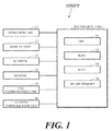
- FIG. 1 is a schematic diagram illustrating a block configuration of an MFP 10 according to this embodiment.
- the MFP 10 includes an operation unit 11 serving as an input device such as buttons through which a user inputs various operations, a display unit 12 serving as a display device such as a liquid crystal display (LCD) that displays various kinds of information, a scanner 13 serving as a reading device that reads an image from an original, a printer 14 serving as a printing device that executes printing on a recording medium such as paper, a FAX communication unit 15 serving as a FAX device that performs FAX communications to/from an external facsimile machine (not shown) via a communication line such as a public telephone line, a network communication unit 16 serving as a network communication device that performs communications to/from an external device (not shown) via a network such as a local area network (LAN) or the Internet, and a control unit 20 that controls the entire MFP 10.
- a display unit 12 serving as a display device such as a liquid crystal display (LCD) that displays various kinds of information
- a scanner 13 serving as a reading device that reads an image from an original
- the control unit 20 includes a central processing unit (CPU) 21, a read only memory (ROM) 22 that stores a program for the CPU 21 and different kinds of data, a random access memory (RAM) 23 used as a work area for the CPU 21, and a flash memory 24 of a NAND type or a NOR type serving as an MTD.
- CPU central processing unit
- ROM read only memory
- RAM random access memory
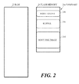
- FIG. 2 is a schematic diagram illustrating a configuration of the RAM 23 and the flash memory 24 within the MFP 10.
- the flash memory 24 stores firmware 24a for a Linux® system.
- the firmware 24a includes a boot loader 24b that is executed when the MFP 10 is booted, a kernel 24c to be expanded onto the RAM 23, a root disk image 24d serving as a compressed file of a root file system.
- the root disk image 24d is a file having a format that can be read by the kernel 23c described later from the MTD via a read-only file system such as Cramfs or Squashfs.
- FIG. 3 is a flowchart of an operation performed when the MFP 10 is booted.
- FIG. 4 is a schematic diagram illustrating a configuration of the RAM 23 and the flash memory 24 when a boot loader 23b has been expanded onto the RAM 23.
- the CPU 21 expands the boot loader 24b on the flash memory 24 onto the RAM 23 as the boot loader 23b as illustrated in FIG. 4 (S31).
- FIG. 5 is a schematic diagram illustrating a configuration of the RAM 23 and the flash memory 24 when the kernel 23c has been expanded onto the RAM 23.
- Step S31 the boot loader 23b executed by the CPU 21 expands the kernel 24c on the flash memory 24 onto the RAM 23 as the kernel 23c as illustrated in FIG. 5 (S32).
- the boot loader 23b determines whether or not a boot mode of the MFP 10 is an update mode for updating the firmware 24a on the flash memory 24 (S33).
- Step S33 When determining in Step S33 that the boot mode is not the update mode, in other words, that the boot mode is a normal boot mode, the boot loader 23b notifies the kernel 23c that the boot mode is the normal boot mode (S34).
- FIG. 6 is a schematic diagram illustrating a configuration of the RAM 23 and the flash memory 24 when the boot mode of the MFP 10 is the normal boot mode.
- the kernel 23c executed by the CPU 21 mounts the root disk image 24d on the flash memory 24 as a root file system (S35). Accordingly, as illustrated in FIG. 6 , the root disk image 24d is read into an area of the RAM 23 not under management of the kernel 23c in unit of the page as the need arises.
- Step S33 When determining in Step S33 that the boot mode is the update mode, the boot loader 23b notifies the kernel 23c that the boot mode is the update mode (S36).
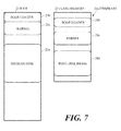
- FIG. 7 is a schematic diagram illustrating a configuration of the RAM 23 and the flash memory 24 when an MTDRAM disk 23a has been generated in the area of the RAM 23 not under the management of the kernel 23c.
- the kernel 23c When notified by the boot loader 23b that the boot mode is the update mode, as illustrated in FIG. 7 , the kernel 23c generates a RAM disk (hereinafter referred to as "MTDRAM disk") 23a serving as an MTD in the area of the RAM 23 not under the management of the kernel 23c (S37).
- MTDRAM disk a RAM disk
- FIG. 8 is a schematic diagram illustrating a configuration of the RAM 23 and the flash memory 24 when a root disk image 23d has been expanded into the MTDRAM disk 23a.
- the kernel 23c expands the root disk image 24d on the flash memory 24 into the MTDRAM disk 23a as the root disk image 23d as illustrated in FIG. 8 (S38).
- FIG. 9 is a schematic diagram illustrating a configuration of the RAM 23 and the flash memory 24 when the boot mode of the MFP 10 is the update mode.
- the kernel 23c mounts the root disk image 23d on the MTDRAM disk 23a as the root file system (S39). Accordingly, as illustrated in FIG. 9 , the root disk image 23d is read into the area of the RAM 23 not under the management of the kernel 23c in unit of the page as the need arises. Note that, the CPU 21 operates in accordance with the root disk image 23d on the MTDRAM disk 23a, and hence can delete the firmware 24a before update from the flash memory 24 and then write the firmware 24a after update into the flash memory 24.
- Step S35 or Step S39 the CPU 21 finishes the operation illustrated in FIG. 3 .
- the MFP 10 stores, in the flash memory 24, the root disk image 24d used in common when the boot mode is the normal boot mode and when the boot mode is the update mode, and can therefore suppress a capacity necessary for the flash memory 24 to a lower level than in a configuration in which a root disk image used when the boot mode is the normal boot mode and a root disk image used when the boot mode is the update mode are separately stored in the flash memory 24.
- the root disk image 23d is not expanded into the area of the RAM 23 not under the management of the kernel 23c, which can increase the capacity of the usable area of the RAM 23.
- the nonvolatile storage device is a flash memory in this embodiment, but may be any storage device other than the flash memory as long as the nonvolatile storage device is the MTD.
- the electronic device according to the present invention is an MFP in this embodiment, but may be any image forming apparatus other than the MFP, such as a copying machine or a printer, or may be any electronic device other than the image forming apparatus such as a general-purpose personal computer.
Landscapes
- Engineering & Computer Science (AREA)
- Software Systems (AREA)
- Theoretical Computer Science (AREA)
- General Engineering & Computer Science (AREA)
- Computer Security & Cryptography (AREA)
- Physics & Mathematics (AREA)
- General Physics & Mathematics (AREA)
- Stored Programmes (AREA)
- Facsimiles In General (AREA)
Abstract
Description
- Unless otherwise indicated herein, the description in this field section or the background section is not prior art to the claims in this application and is not admitted to be prior art by inclusion in this section. The present invention relates to an electronic device including a nonvolatile storage device serving as a memory technology device (MTD).
- As a typical electronic device including a nonvolatile storage device serving as the MTD, there is known an image forming apparatus including a random access memory (RAM) and a flash memory serving as the nonvolatile storage device.
-
FIG. 10 is a schematic diagram illustrating an example of a configuration of aRAM 81 and aflash memory 82 within such a typicalelectronic device 80 as described above. - As illustrated in
FIG. 10 , theelectronic device 80 includes theRAM 81 and theflash memory 82 serving as a nonvolatile storage device. - The
flash memory 82stores firmware 82a for a Linux® system. - The
firmware 82a includes aboot loader 82b that is executed when theelectronic device 80 is booted, akernel 82c to be expanded onto theRAM 81, aroot disk image 82d for normal boot that is a root disk image serving as a compressed file of a root file system and that is used when a boot mode of theelectronic device 80 is a normal boot mode, and aroot disk image 82e for update that is a root disk image used when the boot mode of theelectronic device 80 is an update mode for updating thefirmware 82a on theflash memory 82. - The
root disk image 82d for normal boot is a file having a format that can be read by akernel 81c described later from the MTD via a read-only file system such as Cramfs or Squashfs. On the other hand, theroot disk image 82e for update is a file having a format that can be read by thekernel 81c from an area of theRAM 81 under management of thekernel 81c. The format that can be read by thekernel 81c from the MTD is different from the format that can be read by thekernel 81c from the area of theRAM 81 under the management of thekernel 81c in terms of a mechanism of Linux®. In other words, theroot disk image 82d for normal boot and theroot disk image 82e for update are files having formats different from each other. -
FIG. 11 is a flowchart of an operation performed when theelectronic device 80 is booted.FIG. 12 is a schematic diagram illustrating a configuration of theRAM 81 and theflash memory 82 employed when the boot mode of theelectronic device 80 is the normal boot mode.FIG. 13 is a schematic diagram illustrating a configuration of theRAM 81 and theflash memory 82 employed when the boot mode of theelectronic device 80 is the update mode. - As illustrated in
FIG. 11 , when booted, theelectronic device 80 expands theboot loader 82b on theflash memory 82 onto theRAM 81 as aboot loader 81b (refer toFIG. 12 andFIG. 13 ) (S91). - Subsequently, the
boot loader 81b expands thekernel 82c on theflash memory 82 onto theRAM 81 as thekernel 81c (refer toFIG. 12 andFIG. 13 ) (S92). - Subsequently, the
boot loader 81b determines whether or not the boot mode of theelectronic device 80 is the update mode (S93). - When determining in Step S93 that the boot mode is not the update mode, in other words, that the boot mode is the normal boot mode, the
boot loader 81b notifies thekernel 81c that the boot mode is the normal boot mode (S94). - When notified by the
boot loader 81b that the boot mode is the normal boot mode, thekernel 81c mounts theroot disk image 82d for normal boot on theflash memory 82 as the root file system (S95). Accordingly, as illustrated inFIG. 12 , theroot disk image 82d for normal boot is read into an area of theRAM 81 not under the management of thekernel 81c in unit of a page as the need arises. - When determining in Step S93 that the boot mode is the update mode, the
boot loader 81b notifies thekernel 81c that the boot mode is the update mode (S96). - When notified by the
boot loader 81b that the boot mode is the update mode, as illustrated inFIG. 13 , thekernel 81c expands theroot disk image 82e for update on theflash memory 82 into the area of theRAM 81 under the management of thekernel 81c as aroot disk image 81e for update (S97), and then mounts theroot disk image 81e for update on theRAM 81 as the root file system (S98). Accordingly, as illustrated inFIG. 13 , theroot disk image 81e for update is read into the area of theRAM 81 not under the management of thekernel 81c in unit of the page as the need arises. Note that, theelectronic device 80 operates in accordance with theroot disk image 81e for update on theRAM 81, and hence can delete thefirmware 82a before update from theflash memory 82 and then write thefirmware 82a after update into theflash memory 82. - When the process of Step S95 or Step S98 is finished, the
electronic device 80 finishes the operation illustrated inFIG. 11 . - However, on the
electronic device 80, two kinds of root disk images, theroot disk image 82d for normal boot and theroot disk image 82e for update, need to be stored in theflash memory 82, which increases a capacity necessary for theflash memory 82. - The present invention relates to an electronic device capable of suppressing a capacity necessary for a nonvolatile storage device.
- The electronic device according to the present invention includes a random access memory (RAM), a nonvolatile storage device as a memory technology device (MTD), and firmware that is stored on the nonvolatile storage device. The firmware includes a kernel that is expanded onto the RAM and a root disk image as a root file system.
- The kernel is configured to mount the root disk image on the nonvolatile storage device as the root file system when a boot mode of the electronic device is a normal boot mode.
- The kernel, when the boot mode is an update mode for updating the firmware on the nonvolatile storage device, is configured i) to generate a RAM disk as an MTD in an area of the RAM not under management of the kernel, ii) to expand the root disk image on the nonvolatile storage device into the RAM disk, and iii) to mount the root disk image on the RAM disk as the root file system.
- The invention further relates to a method for booting an electronic device comprising a random access memory (RAM), a nonvolatile storage device as a memory technology device, and firmware that is stored on the nonvolatile storage device, wherein the firmware includes a kernel that is expanded onto the RAM and a root disk image as a root file system. The inventive method comprises the steps of:
- determining whether the boot mode of the electronic device is an update mode for updating the firmware or a normal mode; and
- depending from the result of the determination: either mounting the root disk image on the nonvolatile storage device as the root file system, if the result of the determination is that the boot mode of the electronic device is the normal boot mode; or generating a RAM disk as an memory technology device in an area of the RAM not under management of the kernel, expanding the root disk image on the nonvolatile storage device into the RAM disk, and mounting the root disk image on the RAM disk as the root file system, if the result of the determination is that the boot mode of the electronic device is the update mode for updating the firmware on the nonvolatile storage device.
- Additional features and advantages are described herein, and will be apparent from the following Detailed Description and the figures.
- All drawings are intended to illustrate some aspects and examples of the present invention. The drawings described are only schematic and are non-limiting, and are not necessarily drawn to scale.
-
FIG. 1 is a schematic diagram illustrating a block configuration of a multifunction peripheral (MFP) according to an embodiment of the present invention; -
FIG. 2 is a schematic diagram illustrating a configuration of a RAM and a flash memory within the MFP illustrated inFIG. 1 ; -
FIG. 3 is a flowchart of an operation performed when the MFP illustrated inFIG. 1 is booted; -
FIG. 4 is a schematic diagram illustrating a configuration of the RAM and the flash memory illustrated inFIG. 2 when a boot loader has been expanded onto the RAM; -
FIG. 5 is a schematic diagram illustrating a configuration of the RAM and the flash memory illustrated inFIG. 2 when a kernel has been expanded onto the RAM; -
FIG. 6 is a schematic diagram illustrating a configuration of the RAM and the flash memory when a boot mode of the MFP is a normal boot mode; -
FIG. 7 is a schematic diagram illustrating a configuration of the RAM and the flash memory illustrated inFIG. 2 when an MTDRAM disk has been generated in an area of the RAM not under management of the kernel; -
FIG. 8 is a schematic diagram illustrating a configuration of the RAM and the flash memory illustrated inFIG. 2 when a root disk image has been expanded into the MTDRAM disk; -
FIG. 9 is a schematic diagram illustrating a configuration of the RAM and the flash memory illustrated inFIG. 2 when the boot mode of the MFP is an update mode; -
FIG. 10 is a schematic diagram an example of a configuration of a RAM and a flash memory within a typical electronic device; -
FIG. 11 is a flowchart of an operation performed when the typical electronic device illustrated inFIG. 10 is booted; -
FIG. 12 is a schematic diagram a configuration of the RAM and the flash memory illustrated inFIG. 10 employed when a boot mode of the typical electronic device is a normal boot mode; and -
FIG. 13 is a schematic diagram a configuration of the RAM and the flash memory illustrated inFIG. 10 employed when the boot mode of the typical electronic device is an update mode. - Various embodiments are described below with reference to the figures. It should be understood, however, that numerous variations from the depicted arrangements and functions are possible while remaining in the scope and spirit of the claims. For instance, one or more elements may be added, removed, combined, distributed, substituted, re-positioned, re-ordered, and/or otherwise changed. Further, where this description refers to one or more functions being implemented on and/or by one or more devices, one or more machines, and/or one or more networks, it should be understood that one or more of such entities could carry out one or more of such functions by themselves or in cooperation, and may do so by application of any suitable combination of hardware, firmware, and/or software. For instance, one or more processors may execute one or more sets of programming instructions as at least part of carrying out one or more of the functions described herein.
- Now, an embodiment of the present invention is described with reference to the accompanying drawings.
- First, a description is made of a configuration of an MFP serving as an electronic device according to this embodiment.
-
FIG. 1 is a schematic diagram illustrating a block configuration of an MFP 10 according to this embodiment. - As illustrated in
FIG. 1 , the MFP 10 includes anoperation unit 11 serving as an input device such as buttons through which a user inputs various operations, adisplay unit 12 serving as a display device such as a liquid crystal display (LCD) that displays various kinds of information, ascanner 13 serving as a reading device that reads an image from an original, aprinter 14 serving as a printing device that executes printing on a recording medium such as paper, aFAX communication unit 15 serving as a FAX device that performs FAX communications to/from an external facsimile machine (not shown) via a communication line such as a public telephone line, anetwork communication unit 16 serving as a network communication device that performs communications to/from an external device (not shown) via a network such as a local area network (LAN) or the Internet, and acontrol unit 20 that controls the entire MFP 10. - The
control unit 20 includes a central processing unit (CPU) 21, a read only memory (ROM) 22 that stores a program for theCPU 21 and different kinds of data, a random access memory (RAM) 23 used as a work area for theCPU 21, and aflash memory 24 of a NAND type or a NOR type serving as an MTD. -
FIG. 2 is a schematic diagram illustrating a configuration of theRAM 23 and theflash memory 24 within the MFP 10. - As illustrated in
FIG. 2 , theflash memory 24stores firmware 24a for a Linux® system. - The
firmware 24a includes aboot loader 24b that is executed when the MFP 10 is booted, akernel 24c to be expanded onto theRAM 23, aroot disk image 24d serving as a compressed file of a root file system. - The
root disk image 24d is a file having a format that can be read by thekernel 23c described later from the MTD via a read-only file system such as Cramfs or Squashfs. - Next, a description is made of an operation performed when the MFP 10 is booted.
-
FIG. 3 is a flowchart of an operation performed when the MFP 10 is booted.FIG. 4 is a schematic diagram illustrating a configuration of theRAM 23 and theflash memory 24 when aboot loader 23b has been expanded onto theRAM 23. - As illustrated in
FIG. 3 , when the MFP 10 is booted, theCPU 21 expands theboot loader 24b on theflash memory 24 onto theRAM 23 as theboot loader 23b as illustrated inFIG. 4 (S31). -
FIG. 5 is a schematic diagram illustrating a configuration of theRAM 23 and theflash memory 24 when thekernel 23c has been expanded onto theRAM 23. - When the process of Step S31 is finished, the
boot loader 23b executed by theCPU 21 expands thekernel 24c on theflash memory 24 onto theRAM 23 as thekernel 23c as illustrated inFIG. 5 (S32). - Subsequently, the
boot loader 23b determines whether or not a boot mode of the MFP 10 is an update mode for updating thefirmware 24a on the flash memory 24 (S33). - When determining in Step S33 that the boot mode is not the update mode, in other words, that the boot mode is a normal boot mode, the
boot loader 23b notifies thekernel 23c that the boot mode is the normal boot mode (S34). -
FIG. 6 is a schematic diagram illustrating a configuration of theRAM 23 and theflash memory 24 when the boot mode of the MFP 10 is the normal boot mode. - When notified by the
boot loader 23b that the boot mode is the normal boot mode, thekernel 23c executed by theCPU 21 mounts theroot disk image 24d on theflash memory 24 as a root file system (S35). Accordingly, as illustrated inFIG. 6 , theroot disk image 24d is read into an area of theRAM 23 not under management of thekernel 23c in unit of the page as the need arises. - When determining in Step S33 that the boot mode is the update mode, the
boot loader 23b notifies thekernel 23c that the boot mode is the update mode (S36). -
FIG. 7 is a schematic diagram illustrating a configuration of theRAM 23 and theflash memory 24 when anMTDRAM disk 23a has been generated in the area of theRAM 23 not under the management of thekernel 23c. - When notified by the
boot loader 23b that the boot mode is the update mode, as illustrated inFIG. 7 , thekernel 23c generates a RAM disk (hereinafter referred to as "MTDRAM disk") 23a serving as an MTD in the area of theRAM 23 not under the management of thekernel 23c (S37). -
FIG. 8 is a schematic diagram illustrating a configuration of theRAM 23 and theflash memory 24 when aroot disk image 23d has been expanded into theMTDRAM disk 23a. - After the process of Step S37, the
kernel 23c expands theroot disk image 24d on theflash memory 24 into theMTDRAM disk 23a as theroot disk image 23d as illustrated inFIG. 8 (S38). -
FIG. 9 is a schematic diagram illustrating a configuration of theRAM 23 and theflash memory 24 when the boot mode of the MFP 10 is the update mode. - After the process of Step S38, the
kernel 23c mounts theroot disk image 23d on theMTDRAM disk 23a as the root file system (S39). Accordingly, as illustrated inFIG. 9 , theroot disk image 23d is read into the area of theRAM 23 not under the management of thekernel 23c in unit of the page as the need arises. Note that, theCPU 21 operates in accordance with theroot disk image 23d on theMTDRAM disk 23a, and hence can delete thefirmware 24a before update from theflash memory 24 and then write thefirmware 24a after update into theflash memory 24. - When the process of Step S35 or Step S39 is finished, the
CPU 21 finishes the operation illustrated inFIG. 3 . - As described above, the MFP 10 stores, in the
flash memory 24, theroot disk image 24d used in common when the boot mode is the normal boot mode and when the boot mode is the update mode, and can therefore suppress a capacity necessary for theflash memory 24 to a lower level than in a configuration in which a root disk image used when the boot mode is the normal boot mode and a root disk image used when the boot mode is the update mode are separately stored in theflash memory 24. - Further, on the MFP 10, when the boot mode is the normal boot mode, the
root disk image 23d is not expanded into the area of theRAM 23 not under the management of thekernel 23c, which can increase the capacity of the usable area of theRAM 23. - Note that, the nonvolatile storage device according to the present invention is a flash memory in this embodiment, but may be any storage device other than the flash memory as long as the nonvolatile storage device is the MTD.
- Further, the electronic device according to the present invention is an MFP in this embodiment, but may be any image forming apparatus other than the MFP, such as a copying machine or a printer, or may be any electronic device other than the image forming apparatus such as a general-purpose personal computer.
- It should be understood that various changes and modifications to the embodiments described herein will be apparent to those skilled in the art. Such changes and modifications may be made without departing from the spirit and scope of the present subject matter and without diminishing its intended advantages. It is therefore intended that such changes and modifications be covered by the appended claims.
Claims (11)
- An electronic device (80), comprising:- a random access memory (RAM) (23);- a nonvolatile storage device (24) as a memory technology device; and- firmware (24a) that is stored on the nonvolatile storage device (24), the firmware (24a) including:- a kernel (24c) that is expanded onto the RAM (23); and- a root disk image (24d) as a root file system;wherein a boot mode of the electronic device (80) is either a normal boot mode or a updated boot mode for updating the firmware (24a) on the nonvolatile storage device (24);
wherein the kernel (24c) is configured to mount the root disk image (24d) on the nonvolatile storage device (24) as the root file system, if the boot mode of the electronic device (80) is the normal boot mode; and wherein the kernel (24c) is configured:i) to generate a RAM disk (23a) as an memory technology device in an area of the RAM (23) not under management of the kernel (24c),ii) to expand the root disk image (24d) on the nonvolatile storage device (24) into the RAM disk (23a), andiii) to mount the root disk image (24d) on the RAM disk (23a) as the root file system,if the boot mode of the electronic device (80) is the update mode for updating the firmware (24a) on the nonvolatile storage device (24). - The electronic device (80) according to Claim 1,
wherein the firmware (24a) further includes a boot loader that is executed when the electronic device (80) is booted. - The electronic device (80) according to Claim 2 further comprising:- a central processing unit (CPU)wherein the CPU is configured to expand the boot loader on the nonvolatile storage device (24) onto the RAM (23) as the boot loader when the electronic device (80) is booted.
- The electronic device (80) according to Claim 3,
wherein the CPU is configured to operate in accordance with the root disk image (24d) on the RAM disk (23a), to delete the firmware (24a) before update from the nonvolatile storage device (24), and to write the firmware (24a) after update into the nonvolatile storage device (24). - The electronic device (80) according to Claim 3 or 4,
wherein, when executed by the CPU, the boot loader is configured to expand the kernel (24c) on the nonvolatile storage device (24) onto the RAM (23) as the kernel (24c). - The electronic device (80) according to one of the Claims 2 to 5,
wherein the boot roader is configured to determine whether or not the boot mode of the electronic device (80) is the update mode for updating the firmware (24a) and to notify the kernel (24c) that the boot mode is the normal boot mode or not. - The electronic device (80) according to one of the Claims 1 to 6,
wherein the nonvolatile storage device (24) includes a flash memory. - The electronic device (80) according to one of the Claims 1 to 7,
wherein the root disk image (24d) includes a file having a format which is readable by the kernel (24c) from the memory technology device via a read-only file system such as Cramfs or Squashfs. - The electronic device (80) according to one of the Claims 1 to 8,
wherein the kernel (24c) is configured to mount the root disk image (24d) into an area of the RAM (23) not under management of the kernel (24c) in unit of a page, if the boot mode of the electronic device (80) is the update mode for updating the firmware (24a) on the nonvolatile storage device (24). - The electronic device (80) according to one of the Claims 1 to 9,
wherein the firmware (24a) includes the root disk image (24d) used in common when the boot mode is the normal boot mode and when the boot mode is the update mode. - A method for booting an electronic device (80) comprising a random access memory (RAM) (23), a nonvolatile storage device (24) as a memory technology device, and firmware (24a) that is stored on the nonvolatile storage device (24), the firmware (24a) including a kernel (24c) that is expanded onto the RAM (23) and a root disk image (24d) as a root file system, said method comprising the steps of:- determining whether the boot mode of the electronic device (80) is an update mode for updating the firmware (24a) or a normal mode; and- depending from the result of the determination: either mounting the root disk image (24d) on the nonvolatile storage device (24) as the root file system, if the result of the determination is that the boot mode of the electronic device (80) is the normal boot mode; or generating a RAM disk (23a) as an memory technology device in an area of the RAM (23) not under management of the kernel (24c), expanding the root disk image (24d) on the nonvolatile storage device (24) into the RAM disk (23a), and mounting the root disk image (24d) on the RAM disk (23a) as the root file system, if the result of the determination is that the boot mode of the electronic device (80) is the update mode for updating the firmware (24a) on the nonvolatile storage device (24).
Applications Claiming Priority (1)
| Application Number | Priority Date | Filing Date | Title |
|---|---|---|---|
| JP2013246825A JP5890824B2 (en) | 2013-11-28 | 2013-11-28 | Electronics |
Publications (2)
| Publication Number | Publication Date |
|---|---|
| EP2879051A1 true EP2879051A1 (en) | 2015-06-03 |
| EP2879051B1 EP2879051B1 (en) | 2018-08-15 |
Family
ID=51951707
Family Applications (1)
| Application Number | Title | Priority Date | Filing Date |
|---|---|---|---|
| EP14194543.6A Not-in-force EP2879051B1 (en) | 2013-11-28 | 2014-11-24 | An electronic device including a MTD used temporarily during non-volatile memory file system update |
Country Status (4)
| Country | Link |
|---|---|
| US (1) | US9507584B2 (en) |
| EP (1) | EP2879051B1 (en) |
| JP (1) | JP5890824B2 (en) |
| CN (1) | CN104679503B (en) |
Families Citing this family (15)
| Publication number | Priority date | Publication date | Assignee | Title |
|---|---|---|---|---|
| JP5890824B2 (en) * | 2013-11-28 | 2016-03-22 | 京セラドキュメントソリューションズ株式会社 | Electronics |
| KR101703826B1 (en) * | 2015-10-23 | 2017-02-08 | 한국전자통신연구원 | Apparatus and method for protecting data in flash memory based on abnormal actions in smart device |
| CN106339182A (en) * | 2016-08-25 | 2017-01-18 | 曾美枝 | Memory management method and memory management device |
| JP6887964B2 (en) * | 2018-02-14 | 2021-06-16 | 株式会社日立製作所 | Information processing device and control method of information processing device |
| US11231988B1 (en) | 2018-03-29 | 2022-01-25 | Keep Security, Llc | Systems and methods for secure deletion of information on self correcting secure computer systems |
| US12253908B1 (en) | 2018-03-29 | 2025-03-18 | Keep Security, Llc | Systems and methods for dynamic self-correcting secure computer systems |
| US11263074B1 (en) | 2018-03-29 | 2022-03-01 | Keep Security, Llc | Systems and methods for self correcting secure computer systems |
| US11175981B1 (en) | 2018-03-29 | 2021-11-16 | Keep Security LLC | Systems and methods for dynamic self correcting secure computer systems |
| US10579465B1 (en) | 2018-03-29 | 2020-03-03 | Keep Security LLC | Systems and methods for self correcting secure computer systems |
| US11669389B1 (en) | 2018-03-29 | 2023-06-06 | Keep Security, Llc | Systems and methods for secure deletion of information on self correcting secure computer systems |
| CN110895477B (en) * | 2018-09-13 | 2023-06-02 | 杭州海康威视数字技术股份有限公司 | Equipment starting method, device and equipment |
| CN109408122B (en) * | 2018-09-28 | 2021-05-18 | 联想(北京)有限公司 | Equipment starting method, electronic equipment and computer storage medium |
| US11934680B2 (en) | 2020-02-06 | 2024-03-19 | Arris Enterprises Llc | Systems and methods for booting from NAND flash using squashfs to maximize memory |
| CN112685057B (en) * | 2020-12-18 | 2024-12-10 | 深圳市网心科技有限公司 | Root file system upgrade method, electronic device and computer-readable storage medium |
| US11829771B2 (en) | 2022-04-29 | 2023-11-28 | Red Hat, Inc. | Quick presentation of camera video in a vehicle using Linux |
Citations (2)
| Publication number | Priority date | Publication date | Assignee | Title |
|---|---|---|---|---|
| US7409538B2 (en) * | 2003-12-18 | 2008-08-05 | International Business Machines Corporation | Update in-use flash memory without external interfaces |
| US20090271780A1 (en) * | 2008-04-24 | 2009-10-29 | Moschip Semiconductor Technology Limited | Automatic complete firmware upgrade |
Family Cites Families (11)
| Publication number | Priority date | Publication date | Assignee | Title |
|---|---|---|---|---|
| JP4101004B2 (en) | 2001-09-14 | 2008-06-11 | 株式会社リコー | Image forming apparatus |
| US7355739B2 (en) | 2001-09-14 | 2008-04-08 | Ricoh Company, Ltd. | Image forming device having a memory assignment unit |
| JP2003108398A (en) * | 2001-09-28 | 2003-04-11 | Seiko Epson Corp | Program rewriting method, program rewriting device, and information processing device |
| TWI275032B (en) * | 2005-01-28 | 2007-03-01 | Lite On Technology Corp | Embedded system, automatic loading system and method capable of automatically loading a root file system |
| KR20090060774A (en) * | 2007-12-10 | 2009-06-15 | 한국전자통신연구원 | Firmware and data mirroring device and method in embedded system |
| CN101556547B (en) * | 2009-05-25 | 2012-01-25 | 芯通科技(成都)有限公司 | Safe method and system used for remotely upgrading embedded Linux kernel |
| CN101673211B (en) * | 2009-10-19 | 2014-07-16 | 中兴通讯股份有限公司 | Embedded equipment and starting method thereof |
| JP4886866B2 (en) * | 2010-02-10 | 2012-02-29 | 株式会社バッファロー | Method for speeding up access to main storage device and storage device system |
| US8505003B2 (en) * | 2010-04-28 | 2013-08-06 | Novell, Inc. | System and method for upgrading kernels in cloud computing environments |
| JP5746100B2 (en) * | 2011-12-27 | 2015-07-08 | 京セラドキュメントソリューションズ株式会社 | Image forming apparatus |
| JP5890824B2 (en) * | 2013-11-28 | 2016-03-22 | 京セラドキュメントソリューションズ株式会社 | Electronics |
-
2013
- 2013-11-28 JP JP2013246825A patent/JP5890824B2/en not_active Expired - Fee Related
-
2014
- 2014-11-24 EP EP14194543.6A patent/EP2879051B1/en not_active Not-in-force
- 2014-11-26 US US14/554,148 patent/US9507584B2/en not_active Expired - Fee Related
- 2014-11-27 CN CN201410706083.6A patent/CN104679503B/en not_active Expired - Fee Related
Patent Citations (2)
| Publication number | Priority date | Publication date | Assignee | Title |
|---|---|---|---|---|
| US7409538B2 (en) * | 2003-12-18 | 2008-08-05 | International Business Machines Corporation | Update in-use flash memory without external interfaces |
| US20090271780A1 (en) * | 2008-04-24 | 2009-10-29 | Moschip Semiconductor Technology Limited | Automatic complete firmware upgrade |
Also Published As
| Publication number | Publication date |
|---|---|
| US9507584B2 (en) | 2016-11-29 |
| JP2015106210A (en) | 2015-06-08 |
| JP5890824B2 (en) | 2016-03-22 |
| EP2879051B1 (en) | 2018-08-15 |
| CN104679503A (en) | 2015-06-03 |
| US20150149759A1 (en) | 2015-05-28 |
| CN104679503B (en) | 2018-05-04 |
Similar Documents
| Publication | Publication Date | Title |
|---|---|---|
| EP2879051B1 (en) | An electronic device including a MTD used temporarily during non-volatile memory file system update | |
| US11296943B2 (en) | Information processing apparatus, control method for information processing apparatus, and recording medium | |
| US9454386B2 (en) | Image forming apparatus and method that realize function by installed application | |
| US8775785B2 (en) | Program management method for performing start-up process for programs during start-up of device based on the previous start-up status to prevent occurrence of an out of memory condition | |
| US9600751B2 (en) | Image forming apparatus and control method thereof with a determination whether an application relates to a dynamic update for reflecting change of the network setting without rebooting the apparatus | |
| KR102347702B1 (en) | Information processing apparatus and control method thereof | |
| CN114385249A (en) | Information processing apparatus using exchange file, control method thereof, and storage medium | |
| US12105790B2 (en) | Information processing apparatus, method, and program storage medium | |
| JP2011043932A (en) | Information processing apparatus | |
| US20160239286A1 (en) | Information processing apparatus and installation method | |
| JP6866788B2 (en) | Information processing equipment and programs | |
| US10554841B2 (en) | Image forming apparatus, control method thereof and medium | |
| US20140176979A1 (en) | Management system of information processing apparatus, information processing apparatus, control method of information processing apparatus, and storage medium | |
| JP5873825B2 (en) | Electronic device and application storage program | |
| US10963197B2 (en) | Image processing apparatus that installs application modules, control method therefor, and storage medium | |
| JP6124836B2 (en) | Electronic device and memory management method | |
| US20210136250A1 (en) | Information processing system | |
| US10108380B2 (en) | Information processing apparatus that acquires information from external apparatus and non-transitory computer readable medium storing program | |
| US10447886B2 (en) | Image processing apparatus for updating a non-volatile memory and method controlling image processing apparatus | |
| JP6669101B2 (en) | Electronic device and startup sequence generation program | |
| CN104935767A (en) | Electronic device and data management method | |
| JP5393628B2 (en) | Image forming apparatus | |
| JP6733592B2 (en) | Image forming apparatus and image forming program | |
| US10015348B2 (en) | Image forming apparatus that executes received jobs, control method therefor, and storage medium | |
| US9674381B2 (en) | Electronic device including a job information generating device and access managing device, information management method to enable the electronic device to function, and a non-transitory computer-readable storage medium to store a program for the information management method |
Legal Events
| Date | Code | Title | Description |
|---|---|---|---|
| PUAI | Public reference made under article 153(3) epc to a published international application that has entered the european phase |
Free format text: ORIGINAL CODE: 0009012 |
|
| 17P | Request for examination filed |
Effective date: 20141124 |
|
| AK | Designated contracting states |
Kind code of ref document: A1 Designated state(s): AL AT BE BG CH CY CZ DE DK EE ES FI FR GB GR HR HU IE IS IT LI LT LU LV MC MK MT NL NO PL PT RO RS SE SI SK SM TR |
|
| AX | Request for extension of the european patent |
Extension state: BA ME |
|
| R17P | Request for examination filed (corrected) |
Effective date: 20150902 |
|
| RBV | Designated contracting states (corrected) |
Designated state(s): AL AT BE BG CH CY CZ DE DK EE ES FI FR GB GR HR HU IE IS IT LI LT LU LV MC MK MT NL NO PL PT RO RS SE SI SK SM TR |
|
| 17Q | First examination report despatched |
Effective date: 20151006 |
|
| GRAP | Despatch of communication of intention to grant a patent |
Free format text: ORIGINAL CODE: EPIDOSNIGR1 |
|
| RIC1 | Information provided on ipc code assigned before grant |
Ipc: G06F 9/4401 20180101ALI20180302BHEP Ipc: G06F 9/445 20060101AFI20180302BHEP Ipc: G06F 8/654 20180101ALI20180302BHEP |
|
| INTG | Intention to grant announced |
Effective date: 20180321 |
|
| GRAS | Grant fee paid |
Free format text: ORIGINAL CODE: EPIDOSNIGR3 |
|
| GRAA | (expected) grant |
Free format text: ORIGINAL CODE: 0009210 |
|
| AK | Designated contracting states |
Kind code of ref document: B1 Designated state(s): AL AT BE BG CH CY CZ DE DK EE ES FI FR GB GR HR HU IE IS IT LI LT LU LV MC MK MT NL NO PL PT RO RS SE SI SK SM TR |
|
| REG | Reference to a national code |
Ref country code: CH Ref legal event code: EP Ref country code: GB Ref legal event code: FG4D Ref country code: AT Ref legal event code: REF Ref document number: 1030550 Country of ref document: AT Kind code of ref document: T Effective date: 20180815 |
|
| REG | Reference to a national code |
Ref country code: IE Ref legal event code: FG4D |
|
| REG | Reference to a national code |
Ref country code: DE Ref legal event code: R096 Ref document number: 602014030347 Country of ref document: DE |
|
| REG | Reference to a national code |
Ref country code: FR Ref legal event code: PLFP Year of fee payment: 5 |
|
| REG | Reference to a national code |
Ref country code: NL Ref legal event code: MP Effective date: 20180815 |
|
| REG | Reference to a national code |
Ref country code: LT Ref legal event code: MG4D |
|
| REG | Reference to a national code |
Ref country code: AT Ref legal event code: MK05 Ref document number: 1030550 Country of ref document: AT Kind code of ref document: T Effective date: 20180815 |
|
| PG25 | Lapsed in a contracting state [announced via postgrant information from national office to epo] |
Ref country code: RS Free format text: LAPSE BECAUSE OF FAILURE TO SUBMIT A TRANSLATION OF THE DESCRIPTION OR TO PAY THE FEE WITHIN THE PRESCRIBED TIME-LIMIT Effective date: 20180815 Ref country code: FI Free format text: LAPSE BECAUSE OF FAILURE TO SUBMIT A TRANSLATION OF THE DESCRIPTION OR TO PAY THE FEE WITHIN THE PRESCRIBED TIME-LIMIT Effective date: 20180815 Ref country code: GR Free format text: LAPSE BECAUSE OF FAILURE TO SUBMIT A TRANSLATION OF THE DESCRIPTION OR TO PAY THE FEE WITHIN THE PRESCRIBED TIME-LIMIT Effective date: 20181116 Ref country code: SE Free format text: LAPSE BECAUSE OF FAILURE TO SUBMIT A TRANSLATION OF THE DESCRIPTION OR TO PAY THE FEE WITHIN THE PRESCRIBED TIME-LIMIT Effective date: 20180815 Ref country code: AT Free format text: LAPSE BECAUSE OF FAILURE TO SUBMIT A TRANSLATION OF THE DESCRIPTION OR TO PAY THE FEE WITHIN THE PRESCRIBED TIME-LIMIT Effective date: 20180815 Ref country code: NL Free format text: LAPSE BECAUSE OF FAILURE TO SUBMIT A TRANSLATION OF THE DESCRIPTION OR TO PAY THE FEE WITHIN THE PRESCRIBED TIME-LIMIT Effective date: 20180815 Ref country code: BG Free format text: LAPSE BECAUSE OF FAILURE TO SUBMIT A TRANSLATION OF THE DESCRIPTION OR TO PAY THE FEE WITHIN THE PRESCRIBED TIME-LIMIT Effective date: 20181115 Ref country code: NO Free format text: LAPSE BECAUSE OF FAILURE TO SUBMIT A TRANSLATION OF THE DESCRIPTION OR TO PAY THE FEE WITHIN THE PRESCRIBED TIME-LIMIT Effective date: 20181115 Ref country code: IS Free format text: LAPSE BECAUSE OF FAILURE TO SUBMIT A TRANSLATION OF THE DESCRIPTION OR TO PAY THE FEE WITHIN THE PRESCRIBED TIME-LIMIT Effective date: 20181215 Ref country code: LT Free format text: LAPSE BECAUSE OF FAILURE TO SUBMIT A TRANSLATION OF THE DESCRIPTION OR TO PAY THE FEE WITHIN THE PRESCRIBED TIME-LIMIT Effective date: 20180815 |
|
| PG25 | Lapsed in a contracting state [announced via postgrant information from national office to epo] |
Ref country code: HR Free format text: LAPSE BECAUSE OF FAILURE TO SUBMIT A TRANSLATION OF THE DESCRIPTION OR TO PAY THE FEE WITHIN THE PRESCRIBED TIME-LIMIT Effective date: 20180815 Ref country code: AL Free format text: LAPSE BECAUSE OF FAILURE TO SUBMIT A TRANSLATION OF THE DESCRIPTION OR TO PAY THE FEE WITHIN THE PRESCRIBED TIME-LIMIT Effective date: 20180815 Ref country code: LV Free format text: LAPSE BECAUSE OF FAILURE TO SUBMIT A TRANSLATION OF THE DESCRIPTION OR TO PAY THE FEE WITHIN THE PRESCRIBED TIME-LIMIT Effective date: 20180815 |
|
| PG25 | Lapsed in a contracting state [announced via postgrant information from national office to epo] |
Ref country code: ES Free format text: LAPSE BECAUSE OF FAILURE TO SUBMIT A TRANSLATION OF THE DESCRIPTION OR TO PAY THE FEE WITHIN THE PRESCRIBED TIME-LIMIT Effective date: 20180815 Ref country code: PL Free format text: LAPSE BECAUSE OF FAILURE TO SUBMIT A TRANSLATION OF THE DESCRIPTION OR TO PAY THE FEE WITHIN THE PRESCRIBED TIME-LIMIT Effective date: 20180815 Ref country code: CZ Free format text: LAPSE BECAUSE OF FAILURE TO SUBMIT A TRANSLATION OF THE DESCRIPTION OR TO PAY THE FEE WITHIN THE PRESCRIBED TIME-LIMIT Effective date: 20180815 Ref country code: RO Free format text: LAPSE BECAUSE OF FAILURE TO SUBMIT A TRANSLATION OF THE DESCRIPTION OR TO PAY THE FEE WITHIN THE PRESCRIBED TIME-LIMIT Effective date: 20180815 Ref country code: EE Free format text: LAPSE BECAUSE OF FAILURE TO SUBMIT A TRANSLATION OF THE DESCRIPTION OR TO PAY THE FEE WITHIN THE PRESCRIBED TIME-LIMIT Effective date: 20180815 Ref country code: IT Free format text: LAPSE BECAUSE OF FAILURE TO SUBMIT A TRANSLATION OF THE DESCRIPTION OR TO PAY THE FEE WITHIN THE PRESCRIBED TIME-LIMIT Effective date: 20180815 |
|
| REG | Reference to a national code |
Ref country code: DE Ref legal event code: R097 Ref document number: 602014030347 Country of ref document: DE |
|
| PG25 | Lapsed in a contracting state [announced via postgrant information from national office to epo] |
Ref country code: SM Free format text: LAPSE BECAUSE OF FAILURE TO SUBMIT A TRANSLATION OF THE DESCRIPTION OR TO PAY THE FEE WITHIN THE PRESCRIBED TIME-LIMIT Effective date: 20180815 Ref country code: DK Free format text: LAPSE BECAUSE OF FAILURE TO SUBMIT A TRANSLATION OF THE DESCRIPTION OR TO PAY THE FEE WITHIN THE PRESCRIBED TIME-LIMIT Effective date: 20180815 Ref country code: SK Free format text: LAPSE BECAUSE OF FAILURE TO SUBMIT A TRANSLATION OF THE DESCRIPTION OR TO PAY THE FEE WITHIN THE PRESCRIBED TIME-LIMIT Effective date: 20180815 |
|
| PLBE | No opposition filed within time limit |
Free format text: ORIGINAL CODE: 0009261 |
|
| STAA | Information on the status of an ep patent application or granted ep patent |
Free format text: STATUS: NO OPPOSITION FILED WITHIN TIME LIMIT |
|
| REG | Reference to a national code |
Ref country code: CH Ref legal event code: PL |
|
| 26N | No opposition filed |
Effective date: 20190516 |
|
| PG25 | Lapsed in a contracting state [announced via postgrant information from national office to epo] |
Ref country code: MC Free format text: LAPSE BECAUSE OF FAILURE TO SUBMIT A TRANSLATION OF THE DESCRIPTION OR TO PAY THE FEE WITHIN THE PRESCRIBED TIME-LIMIT Effective date: 20180815 Ref country code: LU Free format text: LAPSE BECAUSE OF NON-PAYMENT OF DUE FEES Effective date: 20181124 |
|
| REG | Reference to a national code |
Ref country code: BE Ref legal event code: MM Effective date: 20181130 |
|
| REG | Reference to a national code |
Ref country code: IE Ref legal event code: MM4A |
|
| PG25 | Lapsed in a contracting state [announced via postgrant information from national office to epo] |
Ref country code: LI Free format text: LAPSE BECAUSE OF NON-PAYMENT OF DUE FEES Effective date: 20181130 Ref country code: CH Free format text: LAPSE BECAUSE OF NON-PAYMENT OF DUE FEES Effective date: 20181130 Ref country code: SI Free format text: LAPSE BECAUSE OF FAILURE TO SUBMIT A TRANSLATION OF THE DESCRIPTION OR TO PAY THE FEE WITHIN THE PRESCRIBED TIME-LIMIT Effective date: 20180815 |
|
| PG25 | Lapsed in a contracting state [announced via postgrant information from national office to epo] |
Ref country code: IE Free format text: LAPSE BECAUSE OF NON-PAYMENT OF DUE FEES Effective date: 20181124 |
|
| PG25 | Lapsed in a contracting state [announced via postgrant information from national office to epo] |
Ref country code: BE Free format text: LAPSE BECAUSE OF NON-PAYMENT OF DUE FEES Effective date: 20181130 |
|
| PG25 | Lapsed in a contracting state [announced via postgrant information from national office to epo] |
Ref country code: MT Free format text: LAPSE BECAUSE OF NON-PAYMENT OF DUE FEES Effective date: 20181124 |
|
| PG25 | Lapsed in a contracting state [announced via postgrant information from national office to epo] |
Ref country code: TR Free format text: LAPSE BECAUSE OF FAILURE TO SUBMIT A TRANSLATION OF THE DESCRIPTION OR TO PAY THE FEE WITHIN THE PRESCRIBED TIME-LIMIT Effective date: 20180815 |
|
| PG25 | Lapsed in a contracting state [announced via postgrant information from national office to epo] |
Ref country code: PT Free format text: LAPSE BECAUSE OF FAILURE TO SUBMIT A TRANSLATION OF THE DESCRIPTION OR TO PAY THE FEE WITHIN THE PRESCRIBED TIME-LIMIT Effective date: 20180815 |
|
| PG25 | Lapsed in a contracting state [announced via postgrant information from national office to epo] |
Ref country code: HU Free format text: LAPSE BECAUSE OF FAILURE TO SUBMIT A TRANSLATION OF THE DESCRIPTION OR TO PAY THE FEE WITHIN THE PRESCRIBED TIME-LIMIT; INVALID AB INITIO Effective date: 20141124 Ref country code: MK Free format text: LAPSE BECAUSE OF NON-PAYMENT OF DUE FEES Effective date: 20180815 Ref country code: CY Free format text: LAPSE BECAUSE OF FAILURE TO SUBMIT A TRANSLATION OF THE DESCRIPTION OR TO PAY THE FEE WITHIN THE PRESCRIBED TIME-LIMIT Effective date: 20180815 |
|
| PGFP | Annual fee paid to national office [announced via postgrant information from national office to epo] |
Ref country code: GB Payment date: 20210930 Year of fee payment: 8 |
|
| PGFP | Annual fee paid to national office [announced via postgrant information from national office to epo] |
Ref country code: DE Payment date: 20210929 Year of fee payment: 8 Ref country code: FR Payment date: 20211109 Year of fee payment: 8 |
|
| REG | Reference to a national code |
Ref country code: DE Ref legal event code: R119 Ref document number: 602014030347 Country of ref document: DE |
|
| GBPC | Gb: european patent ceased through non-payment of renewal fee |
Effective date: 20221124 |
|
| PG25 | Lapsed in a contracting state [announced via postgrant information from national office to epo] |
Ref country code: GB Free format text: LAPSE BECAUSE OF NON-PAYMENT OF DUE FEES Effective date: 20221124 Ref country code: DE Free format text: LAPSE BECAUSE OF NON-PAYMENT OF DUE FEES Effective date: 20230601 |
|
| PG25 | Lapsed in a contracting state [announced via postgrant information from national office to epo] |
Ref country code: FR Free format text: LAPSE BECAUSE OF NON-PAYMENT OF DUE FEES Effective date: 20221130 |